JP6191925B2 - Solar cell module - Google Patents
Solar cell module Download PDFInfo
- Publication number
- JP6191925B2 JP6191925B2 JP2015203901A JP2015203901A JP6191925B2 JP 6191925 B2 JP6191925 B2 JP 6191925B2 JP 2015203901 A JP2015203901 A JP 2015203901A JP 2015203901 A JP2015203901 A JP 2015203901A JP 6191925 B2 JP6191925 B2 JP 6191925B2
- Authority
- JP
- Japan
- Prior art keywords
- solar cell
- electrical connection
- electrode
- connection electrode
- metal film
- Prior art date
- Legal status (The legal status is an assumption and is not a legal conclusion. Google has not performed a legal analysis and makes no representation as to the accuracy of the status listed.)
- Expired - Fee Related
Links
Images


Description
本発明は、太陽電池及び太陽電池モジュールに関する。 The present invention relates to a solar cell and a solar cell module.
近年、環境負荷の小さなエネルギー源として、太陽電池が大いに注目されるようになってきている。その一例として、例えば下記の特許文献1には、光電変換部と、光電変換部の受光面の上に配された受光面電極と、裏面の上に配された裏面電極とを備える太陽電池が記載されている。特許文献1に記載の太陽電池では、受光面電極及び裏面電極のそれぞれが、複数のフィンガー電極部と、複数のフィンガー電極部に電気的に接続されているバスバー部とを備えている。
In recent years, solar cells have attracted a great deal of attention as an energy source with a small environmental load. As an example, for example, in
近年、太陽電池の光電変換効率をさらに向上したいという要望が高まってきている。 In recent years, there is an increasing demand for further improving the photoelectric conversion efficiency of solar cells.
本発明は、斯かる点に鑑みて成されたものであり、その目的は、改善された光電変換効率を有する太陽電池及び太陽電池モジュールを提供することにある。 This invention is made | formed in view of such a point, The objective is to provide the solar cell and solar cell module which have the improved photoelectric conversion efficiency.
本発明に係る太陽電池は、光電変換部と、受光面電極と、裏面電極とを備えている。受光面電極は、光電変換部の受光面の上に配されている。裏面電極は、光電変換部の裏面の上に配されている。裏面電極は、金属膜と、電気的接続用電極とを含む。金属膜は、裏面の少なくとも一部を覆っている。電気的接続用電極は、金属膜の上に配されている。 The solar cell according to the present invention includes a photoelectric conversion unit, a light receiving surface electrode, and a back electrode. The light receiving surface electrode is disposed on the light receiving surface of the photoelectric conversion unit. The back electrode is arranged on the back surface of the photoelectric conversion unit. The back electrode includes a metal film and an electrical connection electrode. The metal film covers at least a part of the back surface. The electrical connection electrode is arranged on the metal film.
本発明に係る太陽電池モジュールは、複数の太陽電池と、複数の太陽電池を電気的に接続している配線材とを備えている。太陽電池は、光電変換部と、受光面電極と、裏面電極とを備えている。受光面電極は、光電変換部の受光面の上に配されている。裏面電極は、光電変換部の裏面の上に配されている。裏面電極は、金属膜と、電気的接続用電極とを含む。金属膜は、裏面の少なくとも一部を覆っている。電気的接続用電極は、金属膜の上に配されている。電気的接続用電極は、配線材と電気的に接続されている。 The solar cell module according to the present invention includes a plurality of solar cells and a wiring member that electrically connects the plurality of solar cells. The solar cell includes a photoelectric conversion unit, a light receiving surface electrode, and a back electrode. The light receiving surface electrode is disposed on the light receiving surface of the photoelectric conversion unit. The back electrode is arranged on the back surface of the photoelectric conversion unit. The back electrode includes a metal film and an electrical connection electrode. The metal film covers at least a part of the back surface. The electrical connection electrode is arranged on the metal film. The electrical connection electrode is electrically connected to the wiring material.
本発明によれば、改善された光電変換効率を有する太陽電池及び太陽電池モジュールを提供することができる。 ADVANTAGE OF THE INVENTION According to this invention, the solar cell and solar cell module which have the improved photoelectric conversion efficiency can be provided.
以下、本発明を実施した好ましい形態の一例について説明する。但し、以下の実施形態は、単なる例示である。本発明は、以下の実施形態に何ら限定されない。 Hereinafter, an example of the preferable form which implemented this invention is demonstrated. However, the following embodiments are merely examples. The present invention is not limited to the following embodiments.
また、実施形態等において参照する各図面において、実質的に同一の機能を有する部材は同一の符号で参照することとする。また、実施形態等において参照する図面は、模式的に記載されたものであり、図面に描画された物体の寸法の比率などは、現実の物体の寸法の比率などとは異なる場合がある。図面相互間においても、物体の寸法比率等が異なる場合がある。具体的な物体の寸法比率等は、以下の説明を参酌して判断されるべきである。 Moreover, in each drawing referred in embodiment etc., the member which has a substantially the same function shall be referred with the same code | symbol. The drawings referred to in the embodiments and the like are schematically described, and the ratio of the dimensions of the objects drawn in the drawings may be different from the ratio of the dimensions of the actual objects. The dimensional ratio of the object may be different between the drawings. The specific dimensional ratio of the object should be determined in consideration of the following description.
(第1の実施形態)
(太陽電池モジュール1の概略構成)
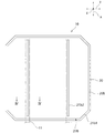
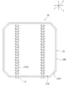
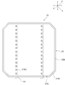
図1に示すように、太陽電池モジュール1は、x方向に沿って配列された複数の太陽電池10を備えている。複数の太陽電池10は、配線材11によって電気的に接続されている。具体的には、x方向に隣接する太陽電池10間が配線材11によって電気的に接続されることによって、複数の太陽電池10が直列または並列に電気的に接続されている。
(First embodiment)
(Schematic configuration of solar cell module 1)
As shown in FIG. 1, the
複数の太陽電池10の裏面側には、第1の保護部材14が配置されている。一方、複数の太陽電池10の受光面側には、第2の保護部材15が配置されている。太陽電池10と第1の保護部材14との間及び太陽電池10と第2の保護部材15との間には、封止材13が設けられている。複数の太陽電池10は、この封止材13により封止されている。
A first
なお、封止材13並びに第1及び第2の保護部材14,15の材料は、特に限定されない。封止材13は、例えば、エチレン・酢酸ビニル共重合体(EVA)やポリビニルブチラール(PVB)等の樹脂により形成することができる。
In addition, the material of the sealing
第1及び第2の保護部材14,15は、例えば、ガラス、樹脂などにより形成することができる。また、太陽電池10の裏面側に配置される第1の保護部材14は、アルミニウム箔などの金属箔を介在させた樹脂フィルムにより構成してもよい。第2の保護部材15は、太陽電池10の受光面側に配置されており、ガラスまたは透光性樹脂等の透光性を有する材料からなる。
The first and second
第1の保護部材14、封止材13、複数の太陽電池10、封止材13、第2の保護部材15を有する積層体の外周には、必要に応じて、Al等の金属製の枠体(図示しない)が取り付けられる。また、第1の保護部材14の表面には、必要に応じて、太陽電池10の出力を外部に取り出すための端子ボックスが設けられる。
On the outer periphery of the laminate having the first
(太陽電池10の構造)
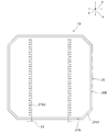
図2〜図4に示すように、太陽電池10は、光電変換部20を有する。光電変換部20は、受光することによって電子や正孔などのキャリアを生成させる部材である。光電変換部20は、例えば、一の導電型を有する結晶性半導体からなる基板と、その基板の一の主面上に配されており、他の導電型を有する第1の非晶質半導体層と、基板の他の主面上に配されており、一の導電型を有する第2の非晶質半導体層とを有するものであってもよい。その場合において、第1及び第2の非晶質半導体層の少なくとも一方と、結晶性半導体基板との間に、実質的に発電に寄与しない厚みのi型非晶質半導体層を設けてもよい。また、光電変換部20は、n型ドーパント拡散領域とp型ドーパント拡散領域とが表面に露出している半導体基板を有するものであってもよい。
(Structure of solar cell 10)
As illustrated in FIGS. 2 to 4, the
本実施形態では、光電変換部20の受光面20a及び裏面20bのそれぞれは、テクスチャ構造を有する。ここで、「テクスチャ構造」とは、表面反射を抑制し、光電変換部の光吸収量を増大させるために形成されている凹凸構造のことをいう。テクスチャ構造の具体例としては、(100)面を有する単結晶シリコン基板の表面に異方性エッチングを施すことによって得られるピラミッド状(四角錐状や、四角錐台状)の凹凸構造が挙げられる。
In the present embodiment, each of the
光電変換部20の受光面20aの上には、受光面電極21aが配されている。受光面電極21aは、複数のフィンガー電極部21a1と、複数のバスバー部21a2とを有する。複数のフィンガー電極部21a1のそれぞれは、y方向に沿って延びるライン状の形状を有する。複数のフィンガー電極部21a1は、x方向に沿って所定の間隔を隔てて配列されている。複数のバスバー部21a2のそれぞれは、x方向に沿って延びている。複数のバスバー部21a2のそれぞれは、複数のフィンガー電極部21a1に電気的に接続されている。
A light receiving
なお、本発明において、受光面電極の構成は特に限定されない。受光面電極は、例えば、複数のフィンガー電極部のみにより構成されており、バスバー部を有さない所謂バスバーレスの電極であってもよい。また、受光面電極21aは、光電変換部20の受光面20aと接するように設けられた透光性導電膜を有するものであっても良い。透光性導電膜は、ITO(Indium Tin Oxide)やZnO等の透光性導電酸化物により構成することができる。
In the present invention, the configuration of the light receiving surface electrode is not particularly limited. For example, the light-receiving surface electrode may be a so-called bus bar-less electrode that includes only a plurality of finger electrode portions and does not have a bus bar portion. Further, the light receiving
受光面電極21aは、主として、バスバー部21a2において配線材11と電気的に接続されている。バスバー部21a2と配線材11との接続は、半田や樹脂接着剤によって行うことができる。
The light receiving
樹脂接着剤は、導電性を有するものであってもよいし、絶縁性を有するものであってもよい。絶縁性を有する樹脂接着剤を用いる場合、バスバー部21a2と配線材11とが接触するように接続を行う必要がある。具体的には、バスバー部21a2が配線材11にめり込むことによって受光面電極21aと配線材11とが電気的に接続されていてもよいし、配線材がバスバー部にめり込むことによって受光面電極21aと配線材11とが電気的に接続されていてもよい。また、配線材及びバスバー部の少なくとも一方の表面に凹凸を設け、その凹凸が他方によりつぶされるようにしてもよい。
The resin adhesive may have conductivity or may have insulating properties. When using the resin adhesive which has insulation, it is necessary to connect so that the bus-bar part 21a2 and the
導電性を有する樹脂接着剤としては、異方導電性を有する樹脂接着剤を好適に用いることができる。 As the resin adhesive having conductivity, a resin adhesive having anisotropic conductivity can be suitably used.
受光面電極21aの材質は、導電材料である限りにおいて特に限定されない。受光面電極21aは、例えば、銀、銅、アルミニウム、チタン、ニッケル、クロムなどの金属や、それらの金属のうちの一種以上を含む合金により構成することができる。また、受光面電極21aは、例えば、上記金属や合金からなる複数の導電層の積層体により構成されていてもよい。
The material of the light receiving
受光面電極21aの形成方法は、特に限定されない。受光面電極21aは、例えば、Agペースト等の導電性ペーストを用いて形成することができる。また、受光面電極21aは、例えば、スパッタ法、蒸着法、スクリーン印刷法或いはメッキ法等を用いて形成する
ことができる。
The formation method of the light-receiving
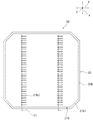
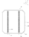
一方、光電変換部20の裏面20bの上には、裏面電極21bが配されている。裏面電極21bは、金属膜21b1と、電気的接続用電極21b2と、透光性導電膜21b3とを含む。
On the other hand, a
なお、本発明において、「金属膜」には、合金膜が含まれるものとする。 In the present invention, the “metal film” includes an alloy film.
金属膜21b1は、裏面20bの少なくとも一部を覆っている。具体的には、本実施形態では、金属膜21b1は、裏面20bの端縁部を除く実質的に全体を覆っている。
The metal film 21b1 covers at least a part of the
金属膜21b1は、金属膜21b1の裏面20bとは反対側の表面にテクスチャ構造に対応した形状の凹凸が存するような厚みを有する。具体的には、金属膜21b1の厚みは、例えば、0.1μm〜5μm程度であることが好ましい。
The metal film 21b1 has such a thickness that unevenness having a shape corresponding to the texture structure exists on the surface opposite to the
金属膜21b1の材質は、特に限定されないが、光反射率が高く、かつ、高い導電性を有するものであることが好ましい。このため、金属膜21b1は、Ag、Al、Cu、Ni、Cr、Ti、Sn、Znなどの金属や、それらの金属の一種以上を含む合金により形成することができる。また、金属膜21b1は、上記金属や合金からなる複数の膜の積層体により構成されていてもよい。 The material of the metal film 21b1 is not particularly limited, but it is preferable that the metal film 21b1 has high light reflectance and high conductivity. For this reason, the metal film 21b1 can be formed of a metal such as Ag, Al, Cu, Ni, Cr, Ti, Sn, Zn, or an alloy containing one or more of these metals. Moreover, the metal film 21b1 may be configured by a laminated body of a plurality of films made of the above metals or alloys.
本実施形態では、具体的には、金属膜21b1は、裏面20bの上に配された第1のAg膜22と、第1のAg膜22の上に配されたAl膜23と、Al膜23の上に配された第2のAg膜24との積層体により構成されている。本実施形態のように中央にAl膜を設けることにより、金属膜21b1の形成コストを低減することができる。また、両側にAg膜を設けることにより、金属膜21b1の反射率を増大させると共に、金属膜21b1の表面の変性を抑制することができる。なお、Al膜23に代えて、第1のAg膜22と第2のAg膜24との間にCu膜を設けてもよい。
Specifically, in the present embodiment, the metal film 21b1 includes a
第1のAg膜22の厚みは、0.1μm〜1μm程度であることが好ましい。Al膜23の厚みは、0.1μm〜1μm程度であることが好ましい。第2のAg膜24の厚みは、0.1μm〜1μm程度であることが好ましいが、これに限定されるものではない。
The thickness of the
金属膜21b1の形成方法は特に限定されない。金属膜21b1は、例えば、Agペースト等の導電性ペーストを用いて形成することができる。また、金属膜21b1は、例えば、スパッタ法、蒸着法、スクリーン印刷法、オフセット印刷法、インクジェット法、或いはメッキ法等を用いて形成することができる。 The formation method of the metal film 21b1 is not particularly limited. The metal film 21b1 can be formed using a conductive paste such as an Ag paste, for example. The metal film 21b1 can be formed using, for example, a sputtering method, a vapor deposition method, a screen printing method, an offset printing method, an ink jet method, a plating method, or the like.
金属膜21b1と裏面20bとの間には、透光性導電膜21b3が配されている。この透光性導電膜21b3により、金属膜21b1の裏面20bに対する密着性が高められている。透光性導電膜21b3は、例えば、ITO(Indium Tin Oxide)や酸化亜鉛等の透光性導電酸化物により形成することができる。なお、透光性導電膜21b3の厚みは、0.5μm〜3μm程度であることが好ましい。
A translucent conductive film 21b3 is disposed between the metal film 21b1 and the
金属膜21b1の上には、電気的接続用電極21b2が配されている。裏面電極21bは、主として、この電気的接続用電極21b2において配線材11と電気的に接続されている。電気的接続用電極21b2と配線材11との接続は、半田や樹脂接着剤を用いて行うことができる。
An electrical connection electrode 21b2 is disposed on the metal film 21b1. The
導電性或いは絶縁性の樹脂接着剤を用いて接続を行う場合、電気的接続用電極21b2が配線材11にめり込むことにより、裏面電極21bと配線材11とが電気的に接続されることが好ましい。また、配線材が電気的接続用電極にめり込むようにしてもよい。また、配線材及び電気的接続用電極の少なくとも一方の表面に凹凸を設け、その凹凸が他方によりつぶされるようにしてもよい。このようにすることで、電気的接続用電極21b2と配線材11との間の接着面積を増加させることができるので、抵抗損失を低減することができる。
When the connection is made using a conductive or insulating resin adhesive, it is preferable that the
また、電気的接続用電極21b2と金属膜21b1との界面および電気的接続用電極21b2の周辺部との少なくとも一方に樹脂層を設けることが好ましい。この樹脂層によって電気的接続用電極21b2と透光性導電膜21b3との界面が保護される。その結果、信頼性を向上させることができる。 In addition, it is preferable to provide a resin layer on at least one of the interface between the electrical connection electrode 21b2 and the metal film 21b1 and the peripheral portion of the electrical connection electrode 21b2. This resin layer protects the interface between the electrical connection electrode 21b2 and the translucent conductive film 21b3. As a result, reliability can be improved.
尚、樹脂層を構成する材料は特に限定されるものではないが、電気的接続用電極21b2或いは金属膜21b1を樹脂型の導電性ペーストを用いて形成する場合、その導電性ペースト中に含まれる樹脂を含むことが好ましい。このようにすることで、電気的接続用電極21b2と金属膜21b1との界面を外部から保護することができ、信頼性を高めることができる。電気的接続用電極21b2の形状は、特に限定されない。本実施形態では、電気的接続用電極21b2は、x方向に沿って延びる線状である。電気的接続用電極21b2は、裏面20bのx方向における一方側端部から他方側端部にまで至っている。電気的接続用電極21b2の幅は、特に限定されないが、例えば、0.05μm〜2mm程度であることが好ましく、0.05μm〜1mm程度であることがより好ましい。
In addition, although the material which comprises a resin layer is not specifically limited, When forming the electrode 21b2 for electrical connection or the metal film 21b1 using a resin-type conductive paste, it is contained in the conductive paste. It is preferable that resin is included. By doing in this way, the interface of the electrode 21b2 for electrical connection and the metal film 21b1 can be protected from the outside, and reliability can be improved. The shape of the electrical connection electrode 21b2 is not particularly limited. In the present embodiment, the electrical connection electrode 21b2 has a linear shape extending along the x direction. The electrical connection electrode 21b2 extends from one end of the
なお、本実施形態では、電気的接続用電極21b2がy方向に沿って2本配列されている例について説明した。但し、本発明は、この構成に限定されない。電気的接続用電極21b2は、1本のみ設けられていてもよし、y方向に沿って3本以上設けられていてもよい。 In the present embodiment, an example in which two electrical connection electrodes 21b2 are arranged along the y direction has been described. However, the present invention is not limited to this configuration. Only one electrical connection electrode 21b2 may be provided, or three or more electrical connection electrodes 21b2 may be provided along the y direction.
電気的接続用電極21b2は、金属膜21b1よりも厚いことが好ましい。具体的には、電気的接続用電極21b2の厚みは、5μm〜20μmの範囲内にあることが好ましい。 The electrical connection electrode 21b2 is preferably thicker than the metal film 21b1. Specifically, the thickness of the electrical connection electrode 21b2 is preferably in the range of 5 μm to 20 μm.
電気的接続用電極21b2の材質は、導電材料である限りにおいて特に限定されない。電気的接続用電極21b2は、例えば、Cu、Ag、Sn等の金属や、それらの金属の少なくとも一種を含む合金により形成することができる。また、電気的接続用電極21b2は、上記金属や合金からなる複数の膜の積層体により構成されていてもよい。 The material of the electrical connection electrode 21b2 is not particularly limited as long as it is a conductive material. The electrical connection electrode 21b2 can be formed of, for example, a metal such as Cu, Ag, or Sn, or an alloy containing at least one of these metals. Further, the electrical connection electrode 21b2 may be formed of a laminate of a plurality of films made of the above metals or alloys.
電気的接続用電極21b2の形成方法は特に限定されない。電気的接続用電極21b2は、例えば、Agペースト等の導電性ペーストを用いて形成することができる。また、電気的接続用電極21b2は、例えば、スパッタ法、蒸着法、スクリーン印刷法、ディスペンス法、オフセット印刷法、インクジェット法等を用いて形成することができる。 The method for forming the electrical connection electrode 21b2 is not particularly limited. The electrical connection electrode 21b2 can be formed using, for example, a conductive paste such as an Ag paste. The electrical connection electrode 21b2 can be formed using, for example, a sputtering method, a vapor deposition method, a screen printing method, a dispensing method, an offset printing method, an ink jet method, or the like.
以上説明したように、本実施形態では、金属膜21b1が配されている。そして、その金属膜21b1により裏面20bの少なくとも一部が覆われている。このため、光電変換部20を透過した光が金属膜21b1によって受光面20a側に反射される。よって、光の有効利用を図ることができる。
As described above, in the present embodiment, the metal film 21b1 is disposed. The metal film 21b1 covers at least a part of the
また、金属膜21b1は、金属膜21b1の裏面20bとは反対側の表面にテクスチャ構造に対応した形状の凹凸が存するような厚みを有する。よって、金属膜21b1で反射された光の光電変換部20における光路長を長くすることができる。従って、より改善された光電変換効率を得ることができる。また、熱膨張係数の違いに起因して生じる金属膜21b1から光電変換部20へのストレスを低減することができる。その結果、光電変換部20に用いる半導体の基板の厚みを180μm以下の薄い厚みにすることができる。
Further, the metal film 21b1 has a thickness such that the surface of the metal film 21b1 opposite to the
透光性導電膜21b3の膜厚は50nm〜200nm程度であることが好ましい。この場合、裏面での反射効率を高めることができる。 The film thickness of the translucent conductive film 21b3 is preferably about 50 nm to 200 nm. In this case, the reflection efficiency on the back surface can be increased.
より改善された光電変換効率を得る観点からは、金属膜21b1の厚みは、0.1μm以上であることが好ましい。より高い信頼性を得る観点からは、金属膜21b1の厚みは、5μm以下であることが好ましい。 From the viewpoint of obtaining improved photoelectric conversion efficiency, the thickness of the metal film 21b1 is preferably 0.1 μm or more. From the viewpoint of obtaining higher reliability, the thickness of the metal film 21b1 is preferably 5 μm or less.
また電気的接続用電極21b2と配線材11との接続をより確実なものにする観点からは、電気的接続用電極21b2は、金属膜21b1よりも厚いことが好ましい。具体的には、電気的接続用電極21b2の厚みは、5μm以上であることが好ましい。但し、電気的接続用電極21b2の厚みが厚すぎると、電気的接続用電極21b2の応力により金属膜から剥離しやすくなる。従って、電気的接続用電極21b2の厚みは、20μm以下であることが好ましい。
Further, from the viewpoint of ensuring the connection between the electrical connection electrode 21b2 and the
本実施形態では、電気的接続用電極21b2は、裏面20bのx方向における一方側端部から他方側端部にまで至っている。このため、温度変化などに起因して配線材11と電気的接続用電極21b2との間に応力が生じた場合であっても、単位面積あたりの応力を小さくすることができる。従って、配線材11の剥離をより効果的に抑制することができる。
In the present embodiment, the electrical connection electrode 21b2 extends from one end portion in the x direction of the
本実施形態では、裏面20bがテクスチャ構造を有する。このため、裏面20bにおいて光が散乱し、光電変換部20内に光が閉じ込められやすくなるため、より改善された光電変換効率を得ることができる。
In the present embodiment, the
さらに、金属膜21b1が、金属膜21b1の裏面20bとは反対側の表面にテクスチャ構造に対応した形状の凹凸が存するような厚みを有する。このため、金属膜21b1と電気的接続用電極21b2との密着強度を高めることができる。
Furthermore, the metal film 21b1 has such a thickness that unevenness having a shape corresponding to the texture structure exists on the surface opposite to the
さらに、金属膜21b1と電気的接続用電極21b2との間、電気的接続用電極21b2周辺に樹脂層を設けることによって、金属膜21b1と電気的接続用電極21b2との界面を外部から保護することができ、信頼性を高めることができる。 Further, by providing a resin layer between the metal film 21b1 and the electrical connection electrode 21b2 and around the electrical connection electrode 21b2, the interface between the metal film 21b1 and the electrical connection electrode 21b2 is protected from the outside. Can improve reliability.
以下、本発明を実施した好ましい形態の他の例について説明する。以下の説明において、上記第1の実施形態と実質的に共通の機能を有する部材を共通の符号で参照し、説明を省略する。 Hereinafter, other examples of preferred embodiments of the present invention will be described. In the following description, members having substantially the same functions as those of the first embodiment are referred to by the same reference numerals, and description thereof is omitted.
上記第1の実施形態では、電気的接続用電極21b2を線状電極としたが、本発明において、電気的接続用電極の形状はこれに限定されない。 In the first embodiment, the electrical connection electrode 21b2 is a linear electrode. However, in the present invention, the shape of the electrical connection electrode is not limited to this.
例えば、図6や図7に示すように、電気的接続用電極21b2を、x方向に沿って配列されており、各々y方向に沿って延びる複数の線状電極により構成してもよい。その場合において、複数の線状電極は、図6に示すように、全体が配線材11の下方に位置するように設けられていてもよいし、図7に示すように、端部が配線材11の外側に位置するように設けられていてもよい。
For example, as shown in FIGS. 6 and 7, the electrical connection electrodes 21b2 may be configured by a plurality of linear electrodes that are arranged along the x direction and each extend along the y direction. In that case, as shown in FIG. 6, the plurality of linear electrodes may be provided so that the whole is positioned below the
また、図8に示すように、電気的接続用電極21b2は、x方向に沿って配列されており、各々、y方向に沿って延びる第1の線状電極部と、第1の線状電極部と交差しており、x方向に沿って延びる複数の第2の線状電極部とを備える複数の電極により構成されていてもよい。 Further, as shown in FIG. 8, the electrical connection electrodes 21b2 are arranged along the x direction, and each of the first linear electrode portions extending along the y direction and the first linear electrodes And a plurality of electrodes including a plurality of second linear electrode portions extending along the x direction.
図9に示すように、電気的接続用電極21b2は、x方向に沿って配列されたV字状の複数の電極により構成されていてもよい。 As shown in FIG. 9, the electrical connection electrode 21b2 may be composed of a plurality of V-shaped electrodes arranged along the x direction.
図10に示すように、電気的接続用電極21b2は、マトリクス状に配列された複数の線状電極により構成されていてもよい。 As shown in FIG. 10, the electrical connection electrode 21b2 may be composed of a plurality of linear electrodes arranged in a matrix.
図11に示すように、電気的接続用電極21b2は、ジグザグ状の電極により構成されていてもよい。 As shown in FIG. 11, the electrical connection electrode 21b2 may be formed of a zigzag electrode.
1 太陽電池モジュール
10 太陽電池
11 配線材
13 封止材
14 第1の保護部材
15 第2の保護部材
20 光電変換部
20a 受光面
20b 裏面
21a 受光面電極
21a1 フィンガー電極部
21a2 バスバー部
21b 裏面電極
21b1 金属膜
21b2 電気的接続用電極
21b3 透光性導電膜
22 第1のAg膜
23 Al膜
24 第2のAg膜
DESCRIPTION OF
Claims (16)
前記太陽電池は、
光電変換部と、
前記光電変換部の受光面の上に配された受光面電極と、
前記光電変換部の裏面の上に配された裏面電極と、
を備え、
前記裏面電極は、前記裏面の少なくとも一部を覆う金属膜と、前記金属膜の直上に配された電気的接続用電極と、前記裏面と前記金属膜との間に設けられた透光性導電膜とからなり、
前記電気的接続用電極は、前記配線材および前記金属膜に挟まれた領域であって第一の方向に2以上並べて配される第二の方向に長手方向を有する接続用電極形成領域に設けられる、
太陽電池モジュール。 A solar cell module comprising a plurality of solar cells, a wiring material that electrically connects the plurality of solar cells, and an adhesive that connects the solar cells and the wiring material,
The solar cell is
A photoelectric conversion unit;
A light receiving surface electrode disposed on the light receiving surface of the photoelectric conversion unit;
A back electrode disposed on the back surface of the photoelectric conversion unit;
With
The back electrode includes a metal film covering at least a part of the back surface, an electrode for electrical connection disposed immediately above the metal film, and a translucent conductive material provided between the back surface and the metal film. Consisting of a membrane,
The electrical connection electrode is provided on the connection electrode formation region having a longitudinal direction in a second direction which is disposed side by side two or more in a first direction A the sandwiched wiring member and the metal film area Be
Solar cell module.
Priority Applications (1)
| Application Number | Priority Date | Filing Date | Title |
|---|---|---|---|
| JP2015203901A JP6191925B2 (en) | 2015-10-15 | 2015-10-15 | Solar cell module |
Applications Claiming Priority (1)
| Application Number | Priority Date | Filing Date | Title |
|---|---|---|---|
| JP2015203901A JP6191925B2 (en) | 2015-10-15 | 2015-10-15 | Solar cell module |
Related Parent Applications (1)
| Application Number | Title | Priority Date | Filing Date |
|---|---|---|---|
| JP2010294493A Division JP5884077B2 (en) | 2010-12-29 | 2010-12-29 | Solar cell and solar cell module |
Publications (3)
| Publication Number | Publication Date |
|---|---|
| JP2016006915A JP2016006915A (en) | 2016-01-14 |
| JP2016006915A5 JP2016006915A5 (en) | 2016-07-28 |
| JP6191925B2 true JP6191925B2 (en) | 2017-09-06 |
Family
ID=55225147
Family Applications (1)
| Application Number | Title | Priority Date | Filing Date |
|---|---|---|---|
| JP2015203901A Expired - Fee Related JP6191925B2 (en) | 2015-10-15 | 2015-10-15 | Solar cell module |
Country Status (1)
| Country | Link |
|---|---|
| JP (1) | JP6191925B2 (en) |
Family Cites Families (15)
| Publication number | Priority date | Publication date | Assignee | Title |
|---|---|---|---|---|
| JP2599470B2 (en) * | 1989-11-16 | 1997-04-09 | 古河電気工業株式会社 | Surface treatment method for Ag-coated Cu material |
| JP2938634B2 (en) * | 1991-10-08 | 1999-08-23 | キヤノン株式会社 | Solar cell module |
| FR2711276B1 (en) * | 1993-10-11 | 1995-12-01 | Neuchatel Universite | Photovoltaic cell and method of manufacturing such a cell. |
| JPH09162430A (en) * | 1995-12-12 | 1997-06-20 | Mitsui Toatsu Chem Inc | Conductive light reflector |
| JP3957461B2 (en) * | 2001-01-22 | 2007-08-15 | シャープ株式会社 | Solar cell and method for manufacturing the same |
| JP2002367434A (en) * | 2001-06-08 | 2002-12-20 | Daido Steel Co Ltd | Corrosion resistant metal member and metal separator for fuel cell using the member |
| JP4212292B2 (en) * | 2002-04-10 | 2009-01-21 | シャープ株式会社 | Solar cell and manufacturing method thereof |
| JP2007207957A (en) * | 2006-01-31 | 2007-08-16 | Sanyo Electric Co Ltd | Optoelectric transducer |
| JP5127207B2 (en) * | 2006-11-28 | 2013-01-23 | 京セラ株式会社 | Solar cell element and solar cell module using the same |
| JP2008159799A (en) * | 2006-12-22 | 2008-07-10 | Sanyo Electric Co Ltd | Photoelectromotive force device |
| EP2264779B1 (en) * | 2008-03-31 | 2018-09-05 | Sharp Kabushiki Kaisha | Solar cell, solar cell string and solar cell module |
| US20100037941A1 (en) * | 2008-08-13 | 2010-02-18 | E. I. Du Pont De Nemours And Company | Compositions and processes for forming photovoltaic devices |
| JP5306112B2 (en) * | 2009-02-17 | 2013-10-02 | 三洋電機株式会社 | Solar cell and solar cell module |
| JP2010192858A (en) * | 2009-02-20 | 2010-09-02 | Mitsubishi Electric Corp | Solar cell and method of manufacturing the same |
| JP4958958B2 (en) * | 2009-10-05 | 2012-06-20 | 三洋電機株式会社 | Method for manufacturing photovoltaic device |
-
2015
- 2015-10-15 JP JP2015203901A patent/JP6191925B2/en not_active Expired - Fee Related
Also Published As
| Publication number | Publication date |
|---|---|
| JP2016006915A (en) | 2016-01-14 |
Similar Documents
| Publication | Publication Date | Title |
|---|---|---|
| JP5884077B2 (en) | Solar cell and solar cell module | |
| JP6586080B2 (en) | Solar cell module and manufacturing method thereof | |
| JP5874011B2 (en) | Solar cell and solar cell module | |
| JP5687506B2 (en) | Solar cell and solar cell module | |
| JP5857237B2 (en) | Solar cell and solar cell module | |
| CN111615752B (en) | Solar cell module | |
| JP5084146B2 (en) | Photovoltaic module | |
| JPWO2020054129A1 (en) | Solar cell devices and solar cell modules | |
| US9373738B2 (en) | Solar module | |
| JP7270631B2 (en) | solar module | |
| JP5799255B2 (en) | Solar cell and solar cell module | |
| JP6029023B2 (en) | SOLAR CELL, SOLAR CELL MODULE, AND SOLAR CELL MANUFACTURING METHOD | |
| JP6191925B2 (en) | Solar cell module | |
| WO2012105153A1 (en) | Photoelectric conversion element | |
| JP5906422B2 (en) | Solar cell and solar cell module | |
| JP2017069442A (en) | Solar battery module | |
| WO2012124464A1 (en) | Solar cell | |
| JP2012160768A (en) | Solar cell | |
| JP2017069291A (en) | Solar battery module | |
| JP6191995B2 (en) | Solar cell module | |
| WO2013046386A1 (en) | Solar cell, solar cell module, and method for manufacturing solar cell | |
| JP2013069898A (en) | Solar cell module and method of manufacturing the same | |
| WO2013046338A1 (en) | Solar cell and solar cell module | |
| JP2015188117A (en) | solar cell | |
| JP2015057863A (en) | Solar cell |
Legal Events
| Date | Code | Title | Description |
|---|---|---|---|
| A621 | Written request for application examination |
Free format text: JAPANESE INTERMEDIATE CODE: A621 Effective date: 20151015 |
|
| A521 | Request for written amendment filed |
Free format text: JAPANESE INTERMEDIATE CODE: A523 Effective date: 20160613 |
|
| A131 | Notification of reasons for refusal |
Free format text: JAPANESE INTERMEDIATE CODE: A131 Effective date: 20160906 |
|
| A521 | Request for written amendment filed |
Free format text: JAPANESE INTERMEDIATE CODE: A523 Effective date: 20161104 |
|
| A131 | Notification of reasons for refusal |
Free format text: JAPANESE INTERMEDIATE CODE: A131 Effective date: 20170404 |
|
| A521 | Request for written amendment filed |
Free format text: JAPANESE INTERMEDIATE CODE: A523 Effective date: 20170602 |
|
| TRDD | Decision of grant or rejection written | ||
| A01 | Written decision to grant a patent or to grant a registration (utility model) |
Free format text: JAPANESE INTERMEDIATE CODE: A01 Effective date: 20170711 |
|
| A61 | First payment of annual fees (during grant procedure) |
Free format text: JAPANESE INTERMEDIATE CODE: A61 Effective date: 20170727 |
|
| R151 | Written notification of patent or utility model registration |
Ref document number: 6191925 Country of ref document: JP Free format text: JAPANESE INTERMEDIATE CODE: R151 |
|
| LAPS | Cancellation because of no payment of annual fees |