JP6166101B2 - Optical semiconductor element storage package and mounting structure including the same - Google Patents

Optical semiconductor element storage package and mounting structure including the same Download PDF

Info

Publication number
JP6166101B2
JP6166101B2 JP2013112981A JP2013112981A JP6166101B2 JP 6166101 B2 JP6166101 B2 JP 6166101B2 JP 2013112981 A JP2013112981 A JP 2013112981A JP 2013112981 A JP2013112981 A JP 2013112981A JP 6166101 B2 JP6166101 B2 JP 6166101B2
Authority
JP
Japan
Prior art keywords
semiconductor element
optical semiconductor
notch
wiring board
substrate
Prior art date
Legal status (The legal status is an assumption and is not a legal conclusion. Google has not performed a legal analysis and makes no representation as to the accuracy of the status listed.)
Active
Application number
JP2013112981A
Other languages
Japanese (ja)
Other versions
JP2014232796A (en
Inventor
茂典 高谷
茂典 高谷
Current Assignee (The listed assignees may be inaccurate. Google has not performed a legal analysis and makes no representation or warranty as to the accuracy of the list.)
Kyocera Corp
Original Assignee
Kyocera Corp
Priority date (The priority date is an assumption and is not a legal conclusion. Google has not performed a legal analysis and makes no representation as to the accuracy of the date listed.)
Filing date
Publication date
Application filed by Kyocera Corp filed Critical Kyocera Corp
Priority to JP2013112981A priority Critical patent/JP6166101B2/en
Publication of JP2014232796A publication Critical patent/JP2014232796A/en
Application granted granted Critical
Publication of JP6166101B2 publication Critical patent/JP6166101B2/en
Active legal-status Critical Current
Anticipated expiration legal-status Critical

Links

Images

Description

本発明は、光半導体素子を収納するための光半導体素子収納用パッケージおよびこれを備えた実装構造体に関する。   The present invention relates to an optical semiconductor element housing package for housing an optical semiconductor element, and a mounting structure including the same.

光半導体素子を収納するための光半導体素子収納用パッケージは、主面を有する基板と、基板の主面上に配置され、貫通孔が形成された側部を有する枠体と、枠体の貫通孔を通って枠体の内側および外側に配置されたコネクタと、枠体の内側における基板の主面上に配置された台座部材と、コネクタに接続された配線基板とを備えている(例えば、特許文献1参照)。   An optical semiconductor element storage package for storing an optical semiconductor element includes a substrate having a main surface, a frame body disposed on the main surface of the substrate and having a side portion in which a through hole is formed, and through the frame body A connector disposed on the inside and outside of the frame body through the hole; a base member disposed on the main surface of the substrate on the inside of the frame body; and a wiring substrate connected to the connector (for example, Patent Document 1).

また、このような光半導体素子収納用パッケージでは、配線基板は台座部材上に配置されており、配線基板は接合部材を介して台座部材に接合されている。   In such an optical semiconductor element housing package, the wiring board is disposed on the pedestal member, and the wiring board is joined to the pedestal member via the joining member.

特開2003−174108号公報JP 2003-174108 A

ここで、このような光半導体素子収納用パッケージでは、光半導体素子の駆動の際に光半導体素子から熱が発生し、この熱が台座部材および配線基板に伝わる。そのため、光半導体素子の駆動による温度変化によって、台座部材および配線基板が熱膨張および熱収縮する可能性がある。   Here, in such an optical semiconductor element housing package, heat is generated from the optical semiconductor element when the optical semiconductor element is driven, and this heat is transmitted to the base member and the wiring board. Therefore, the base member and the wiring board may be thermally expanded and contracted due to a temperature change caused by driving the optical semiconductor element.

このとき、台座部材の熱膨張係数および配線基板の熱膨張係数の違いによって、台座部材および配線基板を接合する接合部材に応力が加わり、接合部材の接合強度が低下する可能性があった。接合部材の接合強度が低下すると、配線基板および台座部材の位置がずれることで、配線基板およびコネクタの位置もずれ、配線基板およびコネクタの接続信頼性が低下する可能性があるという問題点あった。   At this time, due to the difference in the thermal expansion coefficient of the pedestal member and the thermal expansion coefficient of the wiring board, stress is applied to the joining member that joins the pedestal member and the wiring board, and the joining strength of the joining member may be reduced. When the bonding strength of the bonding member is lowered, the positions of the wiring board and the pedestal member are shifted, so that the positions of the wiring board and the connector are also shifted, and the connection reliability of the wiring board and the connector may be lowered. .

本発明は、上記の問題点に鑑みてなされたものであり、その目的は、配線基板およびコネクタの位置がずれることを低減し、配線基板およびコネクタの接続信頼性の低下を抑制できる光半導体素子収納用パッケージを提供することにある。   The present invention has been made in view of the above problems, and an object of the present invention is to reduce the displacement of the positions of the wiring board and the connector, and to suppress the decrease in the connection reliability of the wiring board and the connector. It is to provide a storage package.

本発明に係る光半導体素子収納用パッケージは、主面に光半導体素子を搭載する素子搭載領域を有する基板と、前記素子搭載領域を取り囲むように前記基板の前記主面上に配置
され、貫通孔が形成された側部を有する枠体と、前記枠体の前記貫通孔を通って前記枠体の内側および外側に配置されたコネクタと、前記枠体の内側における前記基板の前記主面上に配置された台座部材と、前記台座部材上に配置された配線基板とを備え、前記台座部材は、上面に第1切欠き部を有しており、前記配線基板が、前記第1切欠き部内に配置され、接合部材を介して前記第1切欠き部の内面に接合されているとともに、前記コネクタに接続されており、前記台座部材の前記上面には、前記第1切欠き部に隣接して第2切欠き部が形成されているとともに、前記配線基板が幅狭部および幅広部を有し、前記幅狭部は前記第2切欠き部によって挟まれている
An optical semiconductor element storage package according to the present invention includes a substrate having an element mounting region for mounting an optical semiconductor element on a main surface, and a through hole disposed on the main surface of the substrate so as to surround the element mounting region. On the main surface of the substrate on the inner side of the frame body, a frame having a side portion formed with a connector, a connector disposed on the inner side and the outer side of the frame body through the through hole of the frame body, A pedestal member disposed on the pedestal member; the pedestal member having a first notch on an upper surface thereof; and the wiring substrate is disposed in the first notch. And is connected to the inner surface of the first cutout portion via a bonding member and connected to the connector, and the upper surface of the base member is adjacent to the first cutout portion. And a second notch is formed Having said wiring board narrow part and the wide part, the narrow portion is sandwiched by said second notch.

本発明に係る光半導体素子収納用パッケージによれば、配線基板およびコネクタの接続
信頼性の低下を抑制できる。
According to the package for housing an optical semiconductor element according to the present invention, it is possible to suppress a decrease in connection reliability between the wiring board and the connector.

本発明に係る実装構造体によれば、上記光半導体素子収納用パッケージを備えていることで、配線基板およびコネクタの接続信頼性の低下を抑制できる。   According to the mounting structure according to the present invention, it is possible to suppress a decrease in connection reliability between the wiring board and the connector by including the optical semiconductor element housing package.

本発明の実施形態に係る光半導体素子収納用パッケージおよびこれを備えた実装構造体であって、蓋体を外した状態での分解斜視図である。1 is an exploded perspective view of a package for housing an optical semiconductor element according to an embodiment of the present invention and a mounting structure including the same, with a lid removed. 図1のX方向から見た光半導体素子収納用パッケージの斜視図である。FIG. 2 is a perspective view of the optical semiconductor element housing package as viewed from the X direction in FIG. 1. 図1の光半導体素子収納用パッケージであって、蓋体を外した状態での平面図である。FIG. 2 is a plan view of the optical semiconductor element storage package of FIG. 1 with a lid removed. 図3のI−I線に沿った断面図である。It is sectional drawing along the II line | wire of FIG. 台座部材、第1切欠き部、第2切欠き部および配線基板を示す斜視図である。It is a perspective view which shows a base member, a 1st notch part, a 2nd notch part, and a wiring board. 第1切欠き部、第2切欠き部および配線基板を示す平面図である。It is a top view which shows a 1st notch part, a 2nd notch part, and a wiring board. 図6のII−II線に沿った断面図である。It is sectional drawing along the II-II line of FIG. コート部材を除いた配線基板の信号配線および導電膜を示す平面図である。It is a top view which shows the signal wiring and electrically conductive film of the wiring board except a coating member.

[光半導体素子収納用パッケージおよび実装構造体]
本発明の実施形態に係る光半導体素子収納用パッケージおよびこれを備えた実装構造体について、図1〜図8を参照しながら説明する。
[Optical Semiconductor Device Storage Package and Mounting Structure]
An optical semiconductor element housing package and a mounting structure including the same according to an embodiment of the present invention will be described with reference to FIGS.

実装構造体1は、光半導体素子2と、光半導体素子収納用パッケージ3とを備えている。   The mounting structure 1 includes an optical semiconductor element 2 and an optical semiconductor element storage package 3.

光半導体素子2は、光信号を電気信号に変換または電気信号を光信号に変換するなど光信号の処理を行なう機能を有する。図1に示すように、光半導体素子2は基板31の主面31a上に配置されている。より具体的には、図1に示すように、基板31の主面31a上には素子用台座部材21が配置されており、光半導体素子2は素子用台座部材21を介して基板31の主面31a上に配置されている。また、図1に示すように、光半導体素子2は光半導体素子収納用パッケージ3に収納されている。   The optical semiconductor element 2 has a function of processing an optical signal such as converting an optical signal into an electric signal or converting an electric signal into an optical signal. As shown in FIG. 1, the optical semiconductor element 2 is disposed on the main surface 31 a of the substrate 31. More specifically, as shown in FIG. 1, an element pedestal member 21 is disposed on the main surface 31 a of the substrate 31. It arrange | positions on the surface 31a. As shown in FIG. 1, the optical semiconductor element 2 is accommodated in an optical semiconductor element accommodation package 3.

光半導体素子2としては、例えばレーザダイオードまたはフォトダイオードなどが挙げられる。光半導体素子2は、例えばヒ化ガリウム、ガリウム砒素リンまたは窒化ガリウムなどの半導体材料によって形成できる。   Examples of the optical semiconductor element 2 include a laser diode and a photodiode. The optical semiconductor element 2 can be formed of a semiconductor material such as gallium arsenide, phosphorus gallium arsenide, or gallium nitride.

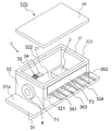
光半導体素子収納用パッケージ3は光半導体素子2を保護する機能を有する。図1に示すように、光半導体素子収納用パッケージ3は光半導体素子2を収納している。また、光半導体素子収納用パッケージ3は、基板31と、枠体32と、コネクタ33と、台座部材34と、配線基板35と、入出力端子36と、シールリング37と、蓋体38とを備える。   The optical semiconductor element housing package 3 has a function of protecting the optical semiconductor element 2. As shown in FIG. 1, the optical semiconductor element housing package 3 houses the optical semiconductor element 2. The optical semiconductor element storage package 3 includes a substrate 31, a frame 32, a connector 33, a base member 34, a wiring substrate 35, an input / output terminal 36, a seal ring 37, and a lid 38. Prepare.

基板31は光半導体素子2を支持する機能を有する。基板31は主面31aを有している。また、基板31の主面31aは、光半導体素子2を搭載されるための素子搭載領域31bを有している。基板31は、1枚の金属板または複数の金属板を積層させた積層体からなる。基板の材料としては、例えば銅、鉄、タングステン、モリブデン、ニッケルまたはコバルトなどの金属、これらの金属を含んだ合金、セラミックス、ガラスあるいは樹脂等が挙げられる。なお、基板31の材料に金属材料を採用すれば、基板31を介して光半導体素子2から発生した熱を放熱できるので、半導体素子収納用パッケージ3の放熱性が向上する。   The substrate 31 has a function of supporting the optical semiconductor element 2. The substrate 31 has a main surface 31a. The main surface 31a of the substrate 31 has an element mounting region 31b for mounting the optical semiconductor element 2. The substrate 31 is composed of a single metal plate or a laminate in which a plurality of metal plates are laminated. Examples of the material for the substrate include metals such as copper, iron, tungsten, molybdenum, nickel, and cobalt, alloys containing these metals, ceramics, glass, and resins. If a metal material is used as the material of the substrate 31, the heat generated from the optical semiconductor element 2 through the substrate 31 can be radiated, so that the heat dissipation of the semiconductor element housing package 3 is improved.

枠体32は、図1、図2および図3に示すように、光半導体素子2(素子搭載領域31b)を取り囲むように基板31の主面31a上に配置されている。枠体32は、第1側部321、第2
側部322、第3側部323および第4側部324を有している。
As shown in FIGS. 1, 2 and 3, the frame 32 is disposed on the main surface 31a of the substrate 31 so as to surround the optical semiconductor element 2 (element mounting region 31b). The frame 32 includes a first side 321 and a second
It has a side portion 322, a third side portion 323, and a fourth side portion 324.

第1側部321は、光ファイバやフェルールなどの光信号を入出力させる部品が挿通され
るための第1貫通孔T1を有する部位である。第2側部322は、コネクタ33が挿通された
第2貫通孔T2を有する部位である。なお、本実施形態の第2側部322は第1側部321に隣接しているが、これには限られない。第3側部323は第1側部321と対向している部位である。第4側部324は、入出力端子36が挿通された第3貫通孔T3を有し、第1側部321に隣接している部位である。なお、第4側部324は第2側部322に対向している。
The first side portion 321 is a portion having a first through hole T1 through which a component that inputs and outputs an optical signal such as an optical fiber or a ferrule is inserted. The second side portion 322 is a portion having a second through hole T2 through which the connector 33 is inserted. In addition, although the 2nd side part 322 of this embodiment is adjacent to the 1st side part 321, it is not restricted to this. The third side part 323 is a part facing the first side part 321. The fourth side portion 324 has a third through hole T3 through which the input / output terminal 36 is inserted, and is a portion adjacent to the first side portion 321. The fourth side portion 324 faces the second side portion 322.

また、図4に示すように、本実施形態では、枠体32および台座部材34が一体形成されている。なお、枠体32および台座部材34を一体形成せずに、それぞれ別体として形成してもよい。   Further, as shown in FIG. 4, in this embodiment, the frame body 32 and the base member 34 are integrally formed. The frame body 32 and the base member 34 may be formed separately from each other without being integrally formed.

枠体32の材料としては、例えば銅、鉄、タングステン、モリブデン、ニッケルまたはコバルトなどの金属、これらの金属を含んだ合金、セラミックス、ガラスあるいは樹脂等が挙げられる。なお、本実施形態の枠体32では、金属または合金が採用されている。これによって、光半導体素子2の駆動の熱を枠体32で放熱しやすくなる。   Examples of the material of the frame 32 include metals such as copper, iron, tungsten, molybdenum, nickel, and cobalt, alloys containing these metals, ceramics, glass, and resins. In the frame body 32 of the present embodiment, a metal or an alloy is employed. As a result, heat for driving the optical semiconductor element 2 can be easily radiated by the frame 32.

枠体32の外側における第1側部321上には、光ファイバやフェルールなどの部品を保持
するための保持部材4がろう材などを介して接合されている。保持部材4によって保持された光ファイバやフェルールなどは、第1側部321の第1貫通孔T1に挿通され、枠体32
の内側に位置する光半導体素子2に光接続される。
On the first side portion 321 outside the frame 32, a holding member 4 for holding components such as an optical fiber and a ferrule is joined via a brazing material or the like. An optical fiber, a ferrule, and the like held by the holding member 4 are inserted into the first through hole T1 of the first side portion 321 and the frame body 32 is inserted.
Is optically connected to the optical semiconductor element 2 located inside the.

コネクタ33は、配線基板35および外部のケーブル(不図示)を接続する機能を有する。図4に示すように、コネクタ33は、第2貫通孔T2を通って枠体32の外側および内側に位置している。また、コネクタ33は、中心導体331および外周導体332を有している。   The connector 33 has a function of connecting the wiring board 35 and an external cable (not shown). As shown in FIG. 4, the connector 33 is located outside and inside the frame 32 through the second through hole T2. Further, the connector 33 has a center conductor 331 and an outer peripheral conductor 332.

図4に示すように、中心導体331は枠体32の内側および外側に延在している。中心導体331は外周導体332によって取り囲まれている。中心導体331は、外周導体332の中心軸33a
を通過して枠体32の内側および外側に延在している。なお、中心導体331および外周導体332の間には、ガラスなどの誘電性材料は配置されている。
As shown in FIG. 4, the center conductor 331 extends inside and outside the frame body 32. The center conductor 331 is surrounded by the outer conductor 332. The center conductor 331 is the center axis 33a of the outer conductor 332.
And extends inside and outside the frame 32. A dielectric material such as glass is disposed between the center conductor 331 and the outer conductor 332.

外周導体332は、中心導体331の外周を取り囲むように配置されている。外周導体332は
中心導体331を保持している。図3および図4に示すように、外周導体332は、枠体32の外側における第2側部322上に配置されている。外周導体332は、枠体32の外側における第2側部322の表面に銀ろうなどのろう材を介して接合されている。より具体的には、外周導
体332は、第2側部322における第2貫通孔T2の周囲の表面に接合されている。
The outer peripheral conductor 332 is disposed so as to surround the outer periphery of the center conductor 331. The outer peripheral conductor 332 holds the center conductor 331. As shown in FIGS. 3 and 4, the outer peripheral conductor 332 is disposed on the second side portion 322 outside the frame body 32. The outer peripheral conductor 332 is joined to the surface of the second side portion 322 outside the frame 32 via a brazing material such as silver brazing. More specifically, the outer peripheral conductor 332 is joined to the surface around the second through hole T2 in the second side portion 322.

外周導体332は中心軸33aを有している。外周導体332の中心軸33aは第2貫通孔T2に重なっている。中心導体331は、中心軸33aに沿って配置され、誘電性材料を介して外周
導体332によって保持される。なお、図2に示すように、本実施形態の外周導体332は円筒状であるが、これに限定されない。
The outer peripheral conductor 332 has a central axis 33a. The central axis 33a of the outer peripheral conductor 332 overlaps the second through hole T2. The central conductor 331 is disposed along the central axis 33a and is held by the outer peripheral conductor 332 via a dielectric material. As shown in FIG. 2, the outer peripheral conductor 332 of the present embodiment is cylindrical, but is not limited to this.

図4に示すように、コネクタ33では、中心導体331の一部は枠体32の外側に位置し、中
心導体331の他の一部は枠体32の内側に位置している。枠体32の外側に位置するコネクタ33の中心導体331には外部のケーブルが接続され、枠体32の内側に位置するコネクタ33の中心導体331には配線基板35が接続される。
As shown in FIG. 4, in the connector 33, a part of the center conductor 331 is located outside the frame body 32, and the other part of the center conductor 331 is located inside the frame body 32. An external cable is connected to the center conductor 331 of the connector 33 located outside the frame 32, and the wiring board 35 is connected to the center conductor 331 of the connector 33 located inside the frame 32.

本実施形態のコネクタ33は、同軸コネクタ構造を採用している。コネクタ33が同軸コネクタ構造である場合には、例えば、鉄−ニッケル−コバルト合金等の金属からなる外周導体332の中心軸33aに同じく鉄−ニッケル−コバルト合金等の金属からなる中心導体331がガラス材を介して固定されている。   The connector 33 of this embodiment employs a coaxial connector structure. When the connector 33 has a coaxial connector structure, for example, the central conductor 331 made of a metal such as iron-nickel-cobalt alloy is formed on the central axis 33a of the outer peripheral conductor 332 made of a metal such as iron-nickel-cobalt alloy. It is fixed through the material.

中心導体331および外周導体332の材料は、例えば銅、鉄、タングステン、モリブデン、ニッケルまたはコバルトなどの金属、これらの金属を含んだ合金が挙げられる。   Examples of the material of the center conductor 331 and the outer conductor 332 include metals such as copper, iron, tungsten, molybdenum, nickel, and cobalt, and alloys containing these metals.

台座部材34は配線基板35を支持する機能を有する。台座部材34は、枠体32の内側における基板31の主面31a上に配置されている。また、台座部材34は枠体32の第2貫通孔T2に隣り合っている。   The base member 34 has a function of supporting the wiring board 35. The pedestal member 34 is disposed on the main surface 31 a of the substrate 31 inside the frame 32. The base member 34 is adjacent to the second through hole T2 of the frame 32.

また、図4に示すように、本実施形態の台座部材34は枠体32と一体形成されている。これによって、枠体32とは別の部材として台座部材34を備える必要がなくなるので、光半導体素子収納用パッケージ3の部品点数が少なくなる。なお、本実施形態の台座部材34は枠体32と一体形成されているが、これには限られない。すなわち、台座部材34を他の部材と一体形成してもよく、例えば台座部材34を外周導体332と一体形成してもよい。   As shown in FIG. 4, the pedestal member 34 of the present embodiment is formed integrally with the frame body 32. As a result, it is not necessary to provide the base member 34 as a member separate from the frame body 32, so that the number of parts of the optical semiconductor element housing package 3 is reduced. In addition, although the base member 34 of this embodiment is integrally formed with the frame 32, it is not restricted to this. That is, the pedestal member 34 may be formed integrally with other members, for example, the pedestal member 34 may be formed integrally with the outer peripheral conductor 332.

台座部材34は、上面に第1切欠き部341および第2切欠き部342を有している。第1切欠き部341は、基板31側に凹む凹部である。第1切欠き部341内には、配線基板35が配置されている。また、図7に示すように、第1切欠き部341の内面には接合部材Bが配置されて
おり、接合部材Bを介して第1切欠き部341の内面および配線基板35が接合されている。
接合部材Bとしては、半田または銀ろうなどのろう材などが挙げられる。
The pedestal member 34 has a first notch 341 and a second notch 342 on the upper surface. The first notch 341 is a recess that is recessed toward the substrate 31 side. A wiring board 35 is disposed in the first notch 341. Further, as shown in FIG. 7, the joining member B is disposed on the inner surface of the first notch 341, and the inner surface of the first notch 341 and the wiring board 35 are joined via the joining member B. Yes.
Examples of the bonding member B include a solder material such as solder or silver solder.

また、第2切欠き部342は基板31側に凹む凹部であり、第1切欠き部341に隣接して形成されている。また、本実施形態の第2切欠き部342は平面視して円弧状である。また、図
5および図6に示すように、本実施形態の第2切欠き部342は、第1切欠き部341における枠体32(第2側部322)側の端部に隣接している。また、本実施形態における第2切欠き
部342は、配線基板35を挟んで配線基板35の両側に位置している。
The second notch 342 is a recess recessed toward the substrate 31 and is formed adjacent to the first notch 341. Further, the second notch portion 342 of the present embodiment has an arc shape in plan view. Further, as shown in FIGS. 5 and 6, the second cutout portion 342 of the present embodiment is adjacent to the end portion of the first cutout portion 341 on the frame body 32 (second side portion 322) side. . Further, the second notch 342 in the present embodiment is located on both sides of the wiring board 35 with the wiring board 35 interposed therebetween.

配線基板35は、光半導体素子2およびコネクタ33の中心導体331を接続する機能を有す
る。配線基板35は台座部材34の上面に配置されている。また、配線基板35は、台座部材34の第1切欠き部341内に配置されている。また、配線基板35は、第1切欠き部341の内面に接合部材Bを介して接合されている。すなわち、配線基板35および第1切欠き部341の間
には接合部材Bが介在している。なお、図7に示すように、本実施形態では、配線基板35の下面および配線基板35の側面の一部が、接合部材Bを介して第1切欠き部341の内面に
接合されている。
The wiring board 35 has a function of connecting the optical semiconductor element 2 and the central conductor 331 of the connector 33. The wiring board 35 is disposed on the upper surface of the base member 34. Further, the wiring board 35 is disposed in the first cutout portion 341 of the base member 34. Further, the wiring board 35 is bonded to the inner surface of the first notch 341 via the bonding member B. That is, the bonding member B is interposed between the wiring board 35 and the first notch 341. As shown in FIG. 7, in this embodiment, the lower surface of the wiring board 35 and a part of the side surface of the wiring board 35 are bonded to the inner surface of the first notch 341 via the bonding member B.

配線基板35は、絶縁基板351、信号配線352および導電膜353を有している。絶縁基板351は信号配線352および導電膜353を支持する機能を有している。本実施形態の絶縁基板351
は幅狭部351aおよび幅狭部351aよりも幅の大きい幅広部351bを有している。
The wiring substrate 35 includes an insulating substrate 351, a signal wiring 352, and a conductive film 353. The insulating substrate 351 has a function of supporting the signal wiring 352 and the conductive film 353. Insulating substrate 351 of this embodiment
Has a narrow part 351a and a wide part 351b having a larger width than the narrow part 351a.

絶縁基板351の材料は、例えば酸化アルミニウム質焼結体、ムライト質焼結体、炭化珪
素質焼結体、窒化アルミニウム質焼結体または窒化珪素質焼結体などのセラミックスが挙げられる。
Examples of the material of the insulating substrate 351 include ceramics such as an aluminum oxide sintered body, a mullite sintered body, a silicon carbide sintered body, an aluminum nitride sintered body, or a silicon nitride sintered body.

信号配線352は、光半導体素子2およびコネクタ33の間で電気信号の伝送する機能を有
する。信号配線352は絶縁基板351の上面に配置されている。また、信号配線352は、半田
または銀ろうなどのろう材を介して枠体32の内側に位置するコネクタ33の中心導体331の
端部に接続されている。信号配線352は絶縁基板351の長手方向に延在している。
The signal wiring 352 has a function of transmitting an electrical signal between the optical semiconductor element 2 and the connector 33. The signal wiring 352 is disposed on the upper surface of the insulating substrate 351. Further, the signal wiring 352 is connected to the end of the central conductor 331 of the connector 33 located inside the frame 32 through a brazing material such as solder or silver brazing. The signal wiring 352 extends in the longitudinal direction of the insulating substrate 351.

導電膜353は絶縁基板351の上面に配置されている。また、図7に示すように、本実施形態の導電膜353は、絶縁基板351の下面にも形成されている。また、絶縁基板351の上面に
位置する導電膜353は、信号配線352の両側に位置しており、信号配線352に接触していな
い。また、絶縁基板351の上面および下面に位置する導電膜353は、絶縁基板351の長手方
向に延在している。なお、導電膜353は、例えばグランド電位など一定の電位に設定され
ている。
The conductive film 353 is disposed on the upper surface of the insulating substrate 351. In addition, as shown in FIG. 7, the conductive film 353 of this embodiment is also formed on the lower surface of the insulating substrate 351. Further, the conductive film 353 located on the upper surface of the insulating substrate 351 is located on both sides of the signal wiring 352 and is not in contact with the signal wiring 352. In addition, the conductive film 353 positioned on the upper surface and the lower surface of the insulating substrate 351 extends in the longitudinal direction of the insulating substrate 351. Note that the conductive film 353 is set to a constant potential such as a ground potential.

また、信号配線352および導電膜353の一部にはアルミナ、クロムなどのコート材Cが形成されている。なお、図6では、コート材Cの形成領域が斜線で示されている。   In addition, a coating material C such as alumina or chromium is formed on part of the signal wiring 352 and the conductive film 353. In FIG. 6, the formation region of the coating material C is indicated by hatching.

配線基板35では、絶縁基板351の上面に信号配線352から離して導電膜353を形成するこ
とで、コプレーナ線路が構成され、信号配線352を伝達する高周波信号を所定のインピー
ダンス値に整合させやすくなり、高周波信号に発生する伝送損失を抑制させ、高周波信号を効率良く入出力させることができる。
In the wiring board 35, a conductive film 353 is formed on the upper surface of the insulating substrate 351 away from the signal wiring 352, so that a coplanar line is formed, and a high-frequency signal transmitted through the signal wiring 352 is easily matched to a predetermined impedance value. The transmission loss generated in the high-frequency signal can be suppressed, and the high-frequency signal can be input / output efficiently.

入出力端子36は、光半導体素子2および外部回路基板(不図示)の間で電気信号の伝送する機能を有する。図1および図2に示すように、入出力端子36は枠体32の第3側部323
の第3貫通孔T3に挿通されている。また、入出力端子36は、基体361と、配線層362と、リード端子363とを有している。
The input / output terminal 36 has a function of transmitting an electrical signal between the optical semiconductor element 2 and an external circuit board (not shown). As shown in FIGS. 1 and 2, the input / output terminal 36 is connected to the third side portion 323 of the frame 32.
The third through hole T3 is inserted. The input / output terminal 36 includes a base 361, a wiring layer 362, and a lead terminal 363.

基体361は、配線層362およびリード端子363を支持する機能を有する。基体361の材料としては、例えば、酸化アルミニウム質焼結体、ムライト質焼結体、炭化珪素質焼結体、窒化アルミニウム質焼結体または窒化珪素質焼結体などのセラミックスが挙げられる。   The base 361 has a function of supporting the wiring layer 362 and the lead terminal 363. Examples of the material of the base 361 include ceramics such as an aluminum oxide sintered body, a mullite sintered body, a silicon carbide sintered body, an aluminum nitride sintered body, or a silicon nitride sintered body.

配線層362は、光半導体素子2が光信号から変換処理した電気信号をリード端子363まで伝送する機能を有する。図1に示すように、複数の配線層362が基体361上に配置されている。また、複数の配線層362は枠体32の外側から内側にかけて延在して配置されている。
枠体32の内側に位置する配線層362の部分は、ボンディングワイヤなどによって光半導体
素子2と電気的に接続される。一方、枠体32の外側に位置する配線層362の部分は、半田
またはろう材などによってリード端子363と電気的に接続される。配線層362の材料としては、例えば銅、銀、金、アルミニウム、ニッケル、モリブデン、タングステン、マンガンまたはクロムなどの金属材料、あるいはこれらの金属材料を含んだ合金が挙げられる。
The wiring layer 362 has a function of transmitting the electrical signal converted from the optical signal by the optical semiconductor element 2 to the lead terminal 363. As shown in FIG. 1, a plurality of wiring layers 362 are arranged on the base 361. The plurality of wiring layers 362 are arranged so as to extend from the outside to the inside of the frame body 32.
A portion of the wiring layer 362 located inside the frame 32 is electrically connected to the optical semiconductor element 2 by a bonding wire or the like. On the other hand, the portion of the wiring layer 362 located outside the frame 32 is electrically connected to the lead terminal 363 by solder or brazing material. Examples of the material of the wiring layer 362 include metal materials such as copper, silver, gold, aluminum, nickel, molybdenum, tungsten, manganese, and chromium, or alloys containing these metal materials.

リード端子363は、光半導体素子2から配線層362を介して伝送される電気信号を外部に伝送する機能を有する。リード端子363は配線層362に接続されている。また、リード端子363は、例えば銅、鉄、タングステン、モリブデン、ニッケルまたはコバルトなどの金属
材料、あるいはこれらの金属材料を含んだ合金からなる。
The lead terminal 363 has a function of transmitting an electrical signal transmitted from the optical semiconductor element 2 via the wiring layer 362 to the outside. The lead terminal 363 is connected to the wiring layer 362. The lead terminal 363 is made of, for example, a metal material such as copper, iron, tungsten, molybdenum, nickel, or cobalt, or an alloy containing these metal materials.

シールリング37は、枠体32および蓋体38を接合する機能を有する。図1に示すように、シールリング37は枠体32の第1側部321〜第4側部324の端面上に配置されており、平面視して光半導体素子2を取り囲んでいる。シールリング37の材料としては、例えば鉄、銅、銀、ニッケル、クロム、コバルト、モリブデンまたはタングステンなどの金属材料、あるいはこれらの金属材料を複数組み合わせた合金などが挙げられる。   The seal ring 37 has a function of joining the frame body 32 and the lid body 38. As shown in FIG. 1, the seal ring 37 is disposed on the end surfaces of the first side portion 321 to the fourth side portion 324 of the frame body 32 and surrounds the optical semiconductor element 2 in plan view. Examples of the material of the seal ring 37 include metal materials such as iron, copper, silver, nickel, chromium, cobalt, molybdenum, and tungsten, or alloys that combine a plurality of these metal materials.

蓋体38は、光半導体素子2を保護する機能を有する。また、図1に示すように、蓋体38は光半導体素子収納用パッケージ3の開口を封止している。蓋体38は、例えばシールリング37と同様の金属材料で形成することができる。   The lid 38 has a function of protecting the optical semiconductor element 2. Further, as shown in FIG. 1, the lid 38 seals the opening of the optical semiconductor element housing package 3. The lid 38 can be formed of a metal material similar to that of the seal ring 37, for example.

光半導体素子収納用パッケージ3では、配線基板35が台座部材34の第1切欠き部341内
に配置されるとともに、第1切欠き部341の内面に接合されている。第1切欠き部341の内面を利用することによって、接合部材Bを介した配線基板35および台座部材34の接合面積を増加させることができるので、配線基板35および台座部材34を強固に接合できる。したがって、例えば光半導体素子2の駆動の熱による温度変化によって、台座部材34および配線基板35が熱膨張および熱収縮して、接合部材Bに応力が加わっても、配線基板35および台座部材34の位置がずれることを低減し、配線基板35およびコネクタ33の接続信頼性の低下を抑制できる。
In the optical semiconductor element housing package 3, the wiring substrate 35 is disposed in the first cutout portion 341 of the base member 34 and is joined to the inner surface of the first cutout portion 341. By using the inner surface of the first notch 341, the bonding area of the wiring board 35 and the pedestal member 34 via the bonding member B can be increased, so that the wiring board 35 and the pedestal member 34 can be firmly bonded. . Therefore, for example, even if the base member 34 and the wiring board 35 are thermally expanded and contracted due to a temperature change due to the driving heat of the optical semiconductor element 2 and stress is applied to the bonding member B, the wiring board 35 and the base member 34 The shift in position can be reduced, and a decrease in connection reliability between the wiring board 35 and the connector 33 can be suppressed.

また、光半導体素子収納用パッケージ3では、台座部材34が、第1切欠き部341に隣接
した第2切欠き部342を有している。ここで、台座部材34は導電性材料で形成されている
ため、配線基板35および台座部材34の間で寄生容量が発生する。そのため、配線基板35の信号配線352に電気信号が伝達する際に、配線基板35および台座部材34の間の寄生容量に
よって、信号配線352の特性インピーダンスが変動してしまう可能性がある。また、例え
ば光半導体素子2の駆動の熱による温度変化によって、台座部材34および配線基板35が熱膨張および熱収縮すると、配線基板35の熱膨張係数および台座部材34の熱膨張係数の違いによって、配線基板35に応力が加わり、配線基板35にクラックが発生し、信号配線352が
断線する可能性がある。
In the optical semiconductor element housing package 3, the pedestal member 34 has a second notch 342 adjacent to the first notch 341. Here, since the pedestal member 34 is formed of a conductive material, a parasitic capacitance is generated between the wiring board 35 and the pedestal member 34. Therefore, when an electric signal is transmitted to the signal wiring 352 of the wiring board 35, the characteristic impedance of the signal wiring 352 may fluctuate due to the parasitic capacitance between the wiring board 35 and the base member 34. Further, for example, when the base member 34 and the wiring board 35 are thermally expanded and contracted due to a temperature change due to the heat of driving the optical semiconductor element 2, due to the difference in the thermal expansion coefficient of the wiring board 35 and the thermal expansion coefficient of the base member 34, There is a possibility that stress is applied to the wiring board 35, a crack occurs in the wiring board 35, and the signal wiring 352 is disconnected.

これに対して、光半導体素子収納用パッケージ3では、台座部材34が第1切欠き部341
に隣接した第2切欠き部342を有している。第2切欠き部342によって台座部材34が切欠かれた分、台座部材34および配線基板35の間で発生する寄生容量を小さくできるので、信号配線352の特性インピーダンスが変動することを低減できる。加えて、第2切欠き部342によって配線基板35および台座部材34の間で発生する応力を分散できるので、配線基板35にクラックが発生することを低減でき、信号配線352が断線することを低減できる。
On the other hand, in the optical semiconductor element storage package 3, the base member 34 has the first notch 341.
The second notch 342 adjacent to the second notch 342 is provided. Since the parasitic capacity generated between the pedestal member 34 and the wiring board 35 can be reduced by the amount of the pedestal member 34 notched by the second notch 342, fluctuations in the characteristic impedance of the signal wiring 352 can be reduced. In addition, since the stress generated between the wiring board 35 and the pedestal member 34 can be dispersed by the second notch 342, the occurrence of cracks in the wiring board 35 can be reduced, and the disconnection of the signal wiring 352 can be reduced. it can.

また、光半導体素子収納用パッケージ3では、第2切欠き部342が、第1切欠き部341における第2貫通孔T2側の端部に隣接している。すなわち、第2切欠き部342がコネクタ33の中心導体331近傍に位置している。これによって、配線基板35および台座部材34の間で発生する寄生容量を小さくできることに加え、コネクタ33(中心導体331)および台座部
材34の間で発生する寄生容量を小さくできる。したがって、信号配線352およびコネクタ33の特性インピーダンスの変動を抑制できる。加えて、第2切欠き部342がコネクタ33の中心導体331近傍に位置することで、コネクタ33(中心導体331)側の配線基板36の端部に生じる応力が低減されるので、コネクタ33(中心導体331)および信号配線352との接合部に加わる応力を低減でき、コネクタ33が信号配線352から剥がれることを抑制することがで
きる。
In the optical semiconductor element housing package 3, the second notch 342 is adjacent to the end of the first notch 341 on the second through hole T 2 side. That is, the second notch 342 is located near the center conductor 331 of the connector 33. Accordingly, the parasitic capacitance generated between the wiring board 35 and the pedestal member 34 can be reduced, and the parasitic capacitance generated between the connector 33 (center conductor 331) and the pedestal member 34 can be reduced. Therefore, fluctuations in the characteristic impedance of the signal wiring 352 and the connector 33 can be suppressed. In addition, since the second notch 342 is positioned in the vicinity of the center conductor 331 of the connector 33, the stress generated at the end of the wiring substrate 36 on the connector 33 (center conductor 331) side is reduced. The stress applied to the joint between the central conductor 331) and the signal wiring 352 can be reduced, and the connector 33 can be prevented from peeling off from the signal wiring 352.

さらに、光半導体素子収納用パッケージ3では、第2切欠き部342が、配線基板35を挟
んで配線基板35の両側に位置している。両側に位置する第2切欠き部342によって、台座
部材34が切欠かれた分、台座部材34および配線基板35の間の寄生容量ならびに台座部材34および中心導体331の間の寄生容量をさらに小さくでき、信号配線352およびコネクタ33の特性インピーダンスの変動を低減できる。加えて、コネクタ33(中心導体331)側の配線
基板36の端部に生じる応力が低減されるので、コネクタ33および信号配線352との接合部
に加わる応力を低減でき、コネクタ33が信号配線352から剥がれることを抑制することが
できる。
Further, in the optical semiconductor element housing package 3, the second notch portions 342 are located on both sides of the wiring board 35 with the wiring board 35 interposed therebetween. The second notch portions 342 located on both sides can further reduce the parasitic capacitance between the pedestal member 34 and the wiring board 35 and the parasitic capacitance between the pedestal member 34 and the central conductor 331 by the amount by which the pedestal member 34 is cut away. Variations in characteristic impedance of the signal wiring 352 and the connector 33 can be reduced. In addition, since the stress generated at the end of the wiring board 36 on the connector 33 (center conductor 331) side is reduced, the stress applied to the joint between the connector 33 and the signal wiring 352 can be reduced, and the connector 33 is connected to the signal wiring 352. It can suppress that it peels from.

また、第2切欠き部342は平面視して円弧状である。これによって、例えば光半導体素
子2の駆動の熱による温度変化によって、配線基板35および台座部材34が熱膨張し、第1切欠き部341に応力が加わった場合でも、配線基板35およびコネクタ33の両側に位置して
第1切欠き部341に隣接する第2切欠き部342の円弧状部分で応力を分散させることができるので、第2切欠き部342に応力を逃がすことができる。
The second notch 342 has an arc shape in plan view. Thereby, for example, even when the wiring board 35 and the base member 34 are thermally expanded due to a temperature change due to heat of driving the optical semiconductor element 2 and stress is applied to the first notch portion 341, the wiring board 35 and the connector 33 Since the stress can be dispersed in the arc-shaped portion of the second notch 342 located on both sides and adjacent to the first notch 341, the stress can be released to the second notch 342.

また、光半導体素子収納用パッケージ3では、配線基板35が幅狭部351aおよび幅広部351bを有し、幅狭部351aは第2切欠き部342によって挟まれている。強度の小さくなりやすい配線基板35の幅狭部351aを円弧状の第2切欠き部342で挟むことで、配線基板35の幅狭部351aに加わる応力を低減できるので、配線基板35およびコネクタ33の接続信頼性の
低下を抑制できる。
In the optical semiconductor element housing package 3, the wiring board 35 has a narrow part 351 a and a wide part 351 b, and the narrow part 351 a is sandwiched between the second notches 342. By sandwiching the narrow portion 351a of the wiring board 35, which tends to be low in strength, between the arc-shaped second notch portions 342, stress applied to the narrow portion 351a of the wiring board 35 can be reduced. It is possible to suppress a decrease in connection reliability.

また、図6に示すように、本実施形態の幅狭部351aは、中心導体331および信号配線352の接合部に比べて枠体32のより内側まで形成されている。これによって、台座部材34の
熱膨張係数および配線基板35の熱膨張係数の差に起因する応力を低減することができるとともに、中心導体331と信号配線352との接合部に生じる応力を低減することができる。
Further, as shown in FIG. 6, the narrow portion 351 a of the present embodiment is formed to the inner side of the frame body 32 as compared with the joint portion of the center conductor 331 and the signal wiring 352. As a result, the stress caused by the difference between the thermal expansion coefficient of the base member 34 and the thermal expansion coefficient of the wiring board 35 can be reduced, and the stress generated at the joint between the center conductor 331 and the signal wiring 352 can be reduced. Can do.

また、図6に示すように、本実施形態の第2切欠き部342は、幅狭部351aに比べて枠体32のより内側まで形成されている。これによって、台座部材34が切欠かれた分、台座部材34および配線基板35の間の寄生容量ならびに台座部材34および中心導体331の間の寄生容
量をさらに小さくでき、信号配線352およびコネクタ33の特性インピーダンスの変動を低
減できる。
Further, as shown in FIG. 6, the second notch portion 342 of the present embodiment is formed to the inner side of the frame body 32 as compared with the narrow portion 351a. As a result, the parasitic capacitance between the pedestal member 34 and the wiring board 35 and the parasitic capacitance between the pedestal member 34 and the central conductor 331 can be further reduced by the amount by which the pedestal member 34 is cut, and the characteristics of the signal wiring 352 and the connector 33 are reduced. Impedance variation can be reduced.

また、実装構造体1は、上記の光半導体素子収納用パッケージ3の内部に光半導体素子2を収納している。光半導体素子収納用パッケージ3では、配線基板35およびコネクタ33の中心導体331の接続信頼性の低下を抑制できる。これによって、光半導体素子2および
コネクタ33の電気的な接続性の低下を抑制することができる。
The mounting structure 1 houses the optical semiconductor element 2 inside the optical semiconductor element storage package 3 described above. In the optical semiconductor element housing package 3, it is possible to suppress a decrease in connection reliability between the wiring board 35 and the central conductor 331 of the connector 33. As a result, it is possible to suppress a decrease in electrical connectivity between the optical semiconductor element 2 and the connector 33.

本発明は上記実施形態に限定されるものではなく、本発明の要旨を逸脱しない範囲において種々の変更、改良などが可能である。   The present invention is not limited to the above-described embodiment, and various changes and improvements can be made without departing from the scope of the present invention.

[光半導体素子収納用パッケージおよび実装構造体の製造方法]
以下、図1に示す光半導体素子収納用パッケージ3および実装構造体1の製造方法を説明する。なお、本発明は以下の実施形態に限定されるものではない。
[Optical Semiconductor Device Storage Package and Mounting Structure Manufacturing Method]
A method for manufacturing the optical semiconductor element housing package 3 and the mounting structure 1 shown in FIG. 1 will be described below. In addition, this invention is not limited to the following embodiment.

まず、基板31、枠体32および保持部材4を作製する。基板31、枠体32および保持部材4のそれぞれは、溶融した金属材料を型枠に鋳込んで固化させたインゴットを金属加工法を用いることによって所定形状に成形することで作製される。そして、枠体32には、第1貫通孔T1〜第3貫通孔T3が形成されるとともに、第2側部322と一体的に、第1切欠き
部341および第2切欠き部342を有する台座部材34が形成される。
First, the substrate 31, the frame body 32, and the holding member 4 are produced. Each of the substrate 31, the frame body 32, and the holding member 4 is manufactured by forming an ingot obtained by casting a molten metal material into a mold and solidifying it into a predetermined shape by using a metal processing method. The frame body 32 is formed with first through holes T1 to third through holes T3, and has a first cutout portion 341 and a second cutout portion 342 integrally with the second side portion 322. A base member 34 is formed.

次に、基体361、配線層362およびリード端子363を有する入出力端子36を作製する。ま
ず、例えば、酸化アルミニウム、窒化ホウ素、窒化アルミニウム、窒化ケイ素、炭化ケイ素または酸化ベリリウムなどのセラミック粉末に、有機バインダー、可塑剤または溶剤等を添加混合した混合物を所定形状に加工する。次いで、タングステンまたはモリブデンなどの高融点金属粉末を準備し、この粉末に有機バインダー、可塑剤または溶剤等を添加混合して金属ペーストを準備する。そして、所定形状に加工した混合物の表面に金属ペーストを所定のパターンに印刷する。そして、これを焼成することによって、金属ペーストを配線層362とし、所定形状に加工した混合物を基体361とする。そして、銀ろうを介して配線層372上にリード端子373を接合することで、入出力端子37が作製される。
Next, the input / output terminal 36 having the base 361, the wiring layer 362, and the lead terminal 363 is manufactured. First, for example, a mixture obtained by adding an organic binder, a plasticizer, a solvent, or the like to ceramic powder such as aluminum oxide, boron nitride, aluminum nitride, silicon nitride, silicon carbide, or beryllium oxide is processed into a predetermined shape. Next, a refractory metal powder such as tungsten or molybdenum is prepared, and an organic binder, a plasticizer or a solvent is added to and mixed with the powder to prepare a metal paste. Then, a metal paste is printed in a predetermined pattern on the surface of the mixture processed into a predetermined shape. Then, by baking this, the metal paste is used as the wiring layer 362, and the mixture processed into a predetermined shape is used as the base 361. Then, the input / output terminal 37 is manufactured by bonding the lead terminal 373 onto the wiring layer 372 via a silver solder.

次に、枠体32を基板31の主面31aに配置し、保持部材4を枠体32の第1側部321の第1
貫通孔T1に重なるように配置するとともに、入出力端子37を第2貫通孔T2に挿入する。
Next, the frame body 32 is disposed on the main surface 31 a of the substrate 31, and the holding member 4 is attached to the first side 321 of the frame body 32.
The input / output terminal 37 is inserted into the second through hole T2 while being arranged so as to overlap the through hole T1.

次に、配線基板35を作製する。基体361および配線層362で説明した作製方法と同様に、セラミック混合物を所定形状に加工し、金属ペーストをセラミック混合物の所定部分に印刷する。そして、これを焼成することによって、金属ペーストを信号配線352、導電膜353、所定形状に加工した混合物を絶縁基板351とする配線基板35が作製される。なお、配線
基板35の所定の部分にコート部材Cを形成してもよい。
Next, the wiring board 35 is produced. Similar to the manufacturing method described for the substrate 361 and the wiring layer 362, the ceramic mixture is processed into a predetermined shape, and a metal paste is printed on a predetermined portion of the ceramic mixture. Then, by firing this, a wiring substrate 35 is produced in which a metal paste is processed into a signal wiring 352, a conductive film 353, and a mixture processed into a predetermined shape is used as an insulating substrate 351. The coating member C may be formed on a predetermined portion of the wiring board 35.

次に、台座部材34の第1切欠き部341に接合部材Bを配置し、この接合部材Bが配置さ
れた第1切欠き部341に配線基板35を配置する。そして、接合部材Bを溶融および固化す
ることによって、配線基板35を第1切欠き部341の内面に接合する。
Next, the joining member B is disposed in the first notch 341 of the base member 34, and the wiring board 35 is disposed in the first notch 341 where the joining member B is disposed. Then, by melting and solidifying the joining member B, the wiring board 35 is joined to the inner surface of the first notch 341.

このとき、接合部材Bを介して配線基板35を台座部材34に接合する際に、配線基板35の位置が変動した場合でも、第1切欠き部341の内面によって配線基板35の位置の変動が抑
制される。すなわち、第1切欠き部341によって、配線基板35の位置ずれを抑制すること
ができ、配線基板35を所望の位置に設けることができるので、中心導体331および信号配
線352の間の高周波信号の伝送特性が良好な光半導体素子収納用パッケージ3を製造でき
る。
At this time, even when the position of the wiring board 35 fluctuates when the wiring board 35 is joined to the pedestal member 34 via the joining member B, the position of the wiring board 35 varies due to the inner surface of the first notch 341. It is suppressed. That is, the first notch 341 can suppress the displacement of the wiring board 35 and the wiring board 35 can be provided at a desired position. Therefore, the high-frequency signal between the center conductor 331 and the signal wiring 352 can be reduced. The optical semiconductor element housing package 3 having good transmission characteristics can be manufactured.

次に、外周導体332の中心軸33aに中心導体331をガラスなどで接合固定させることで、コネクタ33を作製する。そして、コネクタ33を第2貫通孔T2に挿入するとともに、半田を溶融および固化させることによって、コネクタ33を枠体32に固定するとともに、中心導体331および配線基板35を接合する。   Next, the connector 33 is manufactured by bonding and fixing the center conductor 331 to the center axis 33a of the outer conductor 332 with glass or the like. Then, the connector 33 is inserted into the second through hole T2, and the solder 33 is melted and solidified to fix the connector 33 to the frame 32, and the central conductor 331 and the wiring board 35 are joined.

最後に、光半導体素子2を素子用台座部材21を介して基板31の主面31aの素子搭載領域31b上に配置し、光半導体素子2をボンディングワイヤなどを介して配線層362および信
号配線352と電気的に接続する。次いで、光半導体素子収納用パッケージ3を蓋体38にて
封止することで、実装構造体1を作製することができる。
Finally, the optical semiconductor element 2 is disposed on the element mounting region 31b of the main surface 31a of the substrate 31 via the element base member 21, and the optical semiconductor element 2 is disposed on the wiring layer 362 and the signal wiring 352 via bonding wires or the like. Connect electrically. Next, the mounting structure 1 can be manufactured by sealing the optical semiconductor element housing package 3 with the lid 38.

1 実装構造体
2 光半導体素子
3 光半導体素子収納用パッケージ
31 基板
31a 主面
31b 素子搭載領域
32 枠体
321 第1側部
322 第2側部
323 第3側部
324 第4側部
33 コネクタ
331 中心導体
332 外周導体
33a 中心軸
34 台座部材
341 第1切欠き部
342 第2切欠き部
35 配線基板
351 絶縁基板
351a 幅狭部
351b 幅広部
352 信号配線
353 導電膜
36 入出力端子
361 基体
362 配線層
363 リード端子
37 シールリング
38 蓋体
4 保持部材
T1 第1貫通孔
T2 第2貫通孔
T3 第3貫通孔
B 接合部材
C コート材
DESCRIPTION OF SYMBOLS 1 Mounting structure 2 Optical semiconductor element 3 Optical semiconductor element storage package
31 Board
31a Main surface
31b Device mounting area
32 frame
321 first side
322 Second side
323 3rd side
324 4th side
33 Connector
331 Center conductor
332 outer conductor
33a Center axis
34 Base member
341 1st notch
342 Second notch
35 Wiring board
351 Insulation substrate
351a Narrow part
351b Wide part
352 signal wiring
353 conductive film
36 I / O terminals
361 substrate
362 Wiring layer
363 Lead terminal
37 Seal ring
38 Lid 4 Holding member T1 First through hole T2 Second through hole T3 Third through hole B Joining member C Coating material

Claims (5)

主面に光半導体素子を搭載する素子搭載領域を有する基板と、前記素子搭載領域を取り囲むように前記基板の前記主面上に配置され、貫通孔が形成された側部を有する枠体と、前記枠体の前記貫通孔を通って前記枠体の内側および外側に配置されたコネクタと、前記枠体の内側における前記基板の前記主面上に配置された台座部材と、前記台座部材上に配置された配線基板とを備え、
前記台座部材は、上面に第1切欠き部を有しており、
前記配線基板が、前記第1切欠き部内に配置され、接合部材を介して前記第1切欠き部の内面に接合されているとともに、前記コネクタに接続されており、
前記台座部材の前記上面には、前記第1切欠き部に隣接して第2切欠き部が形成されているとともに、前記配線基板が幅狭部および幅広部を有し、前記幅狭部は前記第2切欠き部によって挟まれている光半導体素子収納用パッケージ。
A substrate having an element mounting region for mounting an optical semiconductor element on a main surface; and a frame having a side portion disposed on the main surface of the substrate so as to surround the element mounting region and having a through hole formed thereon; A connector disposed on the inside and outside of the frame through the through-hole of the frame, a pedestal member disposed on the main surface of the substrate on the inside of the frame, and on the pedestal member A wiring board arranged,
The pedestal member has a first notch on the upper surface,
The wiring board is disposed in the first cutout part, joined to the inner surface of the first cutout part via a joining member, and connected to the connector ,
On the upper surface of the pedestal member, a second notch is formed adjacent to the first notch, and the wiring board has a narrow part and a wide part, and the narrow part is An optical semiconductor element storage package sandwiched between the second cutout portions .
前記第2切欠き部は、前記第1切欠き部における前記貫通孔側の端部に隣接している請求項に記載の光半導体素子収納用パッケージ。 2. The optical semiconductor element housing package according to claim 1 , wherein the second notch is adjacent to an end of the first notch on the side of the through hole. 前記第2切欠き部は、前記配線基板を挟んで前記配線基板の両側に位置している請求項またはに記載の光半導体素子収納用パッケージ。 Said second notch portion, an optical semiconductor element storage package according to claim 1 or 2 are located on both sides of the wiring substrate sandwiching the wiring substrate. 前記第2切欠き部は、平面視して円弧状である請求項1〜3のいずれか1つに記載の光半導体素子収納用パッケージ。 Said second notch portion, an optical semiconductor element storage package according to any one of claims 1 to 3 an arc shape in plan view. 請求項1〜のいずれかに記載の光半導体素子収納用パッケージと、
前記基板の前記主面の前記前記素子搭載領域に搭載された光半導体素子とを備える実装構造体。
The package for optical semiconductor element accommodation according to any one of claims 1 to 4 ,
A mounting structure comprising: an optical semiconductor element mounted on the element mounting region of the main surface of the substrate.
JP2013112981A 2013-05-29 2013-05-29 Optical semiconductor element storage package and mounting structure including the same Active JP6166101B2 (en)

Priority Applications (1)

Application Number Priority Date Filing Date Title
JP2013112981A JP6166101B2 (en) 2013-05-29 2013-05-29 Optical semiconductor element storage package and mounting structure including the same

Applications Claiming Priority (1)

Application Number Priority Date Filing Date Title
JP2013112981A JP6166101B2 (en) 2013-05-29 2013-05-29 Optical semiconductor element storage package and mounting structure including the same

Publications (2)

Publication Number Publication Date
JP2014232796A JP2014232796A (en) 2014-12-11
JP6166101B2 true JP6166101B2 (en) 2017-07-19

Family

ID=52126015

Family Applications (1)

Application Number Title Priority Date Filing Date
JP2013112981A Active JP6166101B2 (en) 2013-05-29 2013-05-29 Optical semiconductor element storage package and mounting structure including the same

Country Status (1)

Country Link
JP (1) JP6166101B2 (en)

Families Citing this family (1)

* Cited by examiner, † Cited by third party
Publication number Priority date Publication date Assignee Title
DE102017123342A1 (en) * 2017-10-09 2019-04-11 Schott Ag TO housing with high reflection loss

Family Cites Families (5)

* Cited by examiner, † Cited by third party
Publication number Priority date Publication date Assignee Title
JP2002243992A (en) * 2001-02-20 2002-08-28 Sumitomo Metal Electronics Devices Inc Package, method for attaching package, and tool for attachment
JP3752473B2 (en) * 2002-06-19 2006-03-08 京セラ株式会社 Semiconductor element storage package and semiconductor device
JP2006128323A (en) * 2004-10-27 2006-05-18 Kyocera Corp Semiconductor device and storing package thereof
JP5225825B2 (en) * 2008-12-17 2013-07-03 新光電気工業株式会社 Manufacturing method of semiconductor element storage package and manufacturing method of semiconductor device
JP5610892B2 (en) * 2010-07-22 2014-10-22 京セラ株式会社 Element storage package and semiconductor device including the same

Also Published As

Publication number Publication date
JP2014232796A (en) 2014-12-11

Similar Documents

Publication Publication Date Title
JP5981660B2 (en) Electronic component storage package and electronic device
EP2237316A1 (en) Connection terminal, package using the same and electronic device
JP6243510B2 (en) Electronic component storage package and electronic device
US9805995B2 (en) Element-accommodating package and mounting structure
JP6166101B2 (en) Optical semiconductor element storage package and mounting structure including the same
JP6082114B2 (en) Device storage package and mounting structure
JP6046822B2 (en) Device storage package and mounting structure including the same
JP5812671B2 (en) Device storage package and semiconductor device including the same
JP5873167B2 (en) Semiconductor element storage package and semiconductor device
JP5261104B2 (en) Circuit board and electronic device
JP6829303B2 (en) Insulation substrates, semiconductor packages and semiconductor devices
WO2015088028A1 (en) Element housing package and mounting structure
JP5709427B2 (en) Device storage package and semiconductor device including the same
JP6051095B2 (en) Optical semiconductor element storage package and mounting structure including the same
JP2009283898A (en) Electronic part container, package for storing electronic part using the same and electronic device
JP6162520B2 (en) Package for housing semiconductor element and mounting structure including the same
JP5992785B2 (en) Semiconductor element storage package and semiconductor device
JP6239970B2 (en) TO-CAN type package header and semiconductor device
JP5791258B2 (en) Electronic component storage package and mounting structure
JP6408661B2 (en) TO-CAN type package header and semiconductor device
JP6219693B2 (en) Device storage package and mounting structure including the same
WO2015029880A1 (en) Package for housing elements and mounting structure
JP5725900B2 (en) Semiconductor element storage package and semiconductor device including the same
JP2012234880A (en) Package for housing element, and semiconductor device including the package
JP2006093611A (en) Electronic component accommodating package and electronic device

Legal Events

Date Code Title Description
A621 Written request for application examination

Free format text: JAPANESE INTERMEDIATE CODE: A621

Effective date: 20160115

A131 Notification of reasons for refusal

Free format text: JAPANESE INTERMEDIATE CODE: A131

Effective date: 20161018

A977 Report on retrieval

Free format text: JAPANESE INTERMEDIATE CODE: A971007

Effective date: 20161019

A521 Request for written amendment filed

Free format text: JAPANESE INTERMEDIATE CODE: A523

Effective date: 20161215

TRDD Decision of grant or rejection written
A01 Written decision to grant a patent or to grant a registration (utility model)

Free format text: JAPANESE INTERMEDIATE CODE: A01

Effective date: 20170523

A61 First payment of annual fees (during grant procedure)

Free format text: JAPANESE INTERMEDIATE CODE: A61

Effective date: 20170622

R150 Certificate of patent or registration of utility model

Ref document number: 6166101

Country of ref document: JP

Free format text: JAPANESE INTERMEDIATE CODE: R150