JP6136420B2 - 設計支援装置、ビア追加方法、及びプログラム - Google Patents
設計支援装置、ビア追加方法、及びプログラム Download PDFInfo
- Publication number
- JP6136420B2 JP6136420B2 JP2013058634A JP2013058634A JP6136420B2 JP 6136420 B2 JP6136420 B2 JP 6136420B2 JP 2013058634 A JP2013058634 A JP 2013058634A JP 2013058634 A JP2013058634 A JP 2013058634A JP 6136420 B2 JP6136420 B2 JP 6136420B2
- Authority
- JP
- Japan
- Prior art keywords
- added
- point
- target area
- search
- starting point
- Prior art date
- Legal status (The legal status is an assumption and is not a legal conclusion. Google has not performed a legal analysis and makes no representation as to the accuracy of the status listed.)
- Expired - Fee Related
Links
Images


Classifications
-
- H—ELECTRICITY
- H05—ELECTRIC TECHNIQUES NOT OTHERWISE PROVIDED FOR
- H05K—PRINTED CIRCUITS; CASINGS OR CONSTRUCTIONAL DETAILS OF ELECTRIC APPARATUS; MANUFACTURE OF ASSEMBLAGES OF ELECTRICAL COMPONENTS
- H05K3/00—Apparatus or processes for manufacturing printed circuits
- H05K3/0005—Apparatus or processes for manufacturing printed circuits for designing circuits by computer
-
- G—PHYSICS
- G06—COMPUTING OR CALCULATING; COUNTING
- G06F—ELECTRIC DIGITAL DATA PROCESSING
- G06F30/00—Computer-aided design [CAD]
- G06F30/30—Circuit design
- G06F30/39—Circuit design at the physical level
- G06F30/392—Floor-planning or layout, e.g. partitioning or placement
-
- H—ELECTRICITY
- H05—ELECTRIC TECHNIQUES NOT OTHERWISE PROVIDED FOR
- H05K—PRINTED CIRCUITS; CASINGS OR CONSTRUCTIONAL DETAILS OF ELECTRIC APPARATUS; MANUFACTURE OF ASSEMBLAGES OF ELECTRICAL COMPONENTS
- H05K1/00—Printed circuits
- H05K1/02—Details
- H05K1/11—Printed elements for providing electric connections to or between printed circuits
- H05K1/115—Via connections; Lands around holes or via connections
Landscapes
- Engineering & Computer Science (AREA)
- Computer Hardware Design (AREA)
- Microelectronics & Electronic Packaging (AREA)
- Theoretical Computer Science (AREA)
- Physics & Mathematics (AREA)
- Manufacturing & Machinery (AREA)
- Evolutionary Computation (AREA)
- Geometry (AREA)
- General Engineering & Computer Science (AREA)
- General Physics & Mathematics (AREA)
- Architecture (AREA)
- Design And Manufacture Of Integrated Circuits (AREA)
- Structure Of Printed Boards (AREA)
Description
図1は、本実施形態による設計支援装置の機能構成例を表す図である。図2〜図8は、本実施形態による設計支援装置の動作を説明する図である。
・・・(1)
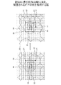
上記のように、一定間隔を信号波長λの1/20とした場合、追加されたビアは、その位置から半径がλ/40の円の範囲内でEMIを適切に抑制すると見なすことができる。以降、その円を「防御エリア」と呼ぶことにする。図4に表す円22は防御エリアの例である。
追加するビアは、信号配線が配置された層(以降「信号層)とグラウンド層とを接続する(このことから、図1ではS1で「SG(Signal Ground)ビア」と表記している)。それにより、ビアを追加するのは、信号層上ではビアを配置可能なエリアであり、且つグラウンド層上ではグラウンドプレーンが存在しているエリアとなる。図2の矩形20は、信号層上で対象となるエリアと、グラウンド層上で対象となるエリアとが重なる、ビアを追加すべき全体のエリア(以降「全体対象エリア」と表記)である。
図4〜図7に表すようなビア32、51の配置は、図1に表す処理を実行することで実現される。次に、図1を参照して、グリッド探索部16を実現させる処理について、詳細に説明する。処理を実行する主体は、ここではグリッド探索部16とする。図1に表す処理は、1つのビア追加対象エリア25のみを対象にして実行される一連の処理の流れを表している。
2、2a CADデータ
3 設定データ
11 入出力部
12 ビア追加対象エリア検索部
13 SGビア追加部
15 開始点設定部
16 グリッド探索部
Claims (6)
- 設計されたプリント基板上でビアを追加すべき対象エリアを特定するエリア特定部と、
前記エリア特定部が特定した前記対象エリアの重心を、前記ビアを追加すべき位置を探索するうえでの開始点として決定する決定部と、
前記ビアを追加すべきか否かを確認する探索点を、前記開始点を中心とする径方向上で起点とする位置を変更しつつ、前記径方向と交差する交差方向に前記起点から予め定められた経路に沿って移動させ、移動後の前記探索点に前記ビアを追加すべきか否か確認することにより、前記ビアを追加すべき位置を決定する探索部と、
を有することを特徴とする設計支援装置。 - 前記探索部は、前記起点の前記径方向上の位置を、前記開始点から順次、離す方向に移動させることにより、前記探索点を渦巻き状に移動させる、
ことを特徴とする請求項1記載の設計支援装置。 - 前記対象エリアは、前記プリント基板上で前記ビアを追加すべき全体対象エリアの境界に沿って前記ビアを配置した場合に、前記全体対象エリア内で前記ビアの影響が及ばないとするエリアである、
ことを特徴とする請求項1、または2記載の設計支援装置。 - 前記探索部は、前記プリント配線板の設計時に設定されたグリッドに沿って、前記探索点を渦巻き状に移動させる、
ことを特徴とする請求項1、2、または3記載の設計支援装置。 - 設計されたプリント基板上に追加すべきビアを追加する設計支援を行う設計支援装置として用いられる情報処理装置に、
前記プリント基板上で前記ビアを追加すべき対象エリアを特定させ、
前記対象エリアの重心を、前記ビアを追加すべき位置を探索するうえでの開始点として決定させ、
前記ビアを追加すべきか否かを確認する探索点を、前記開始点を中心とする径方向上で起点とする位置を変更させつつ、前記径方向と交差する交差方向に前記起点から予め定められた経路に沿って移動させて、移動後の前記探索点に前記ビアを追加すべきか否か確認することにより、前記ビアを追加すべき位置を決定させる、
ことを特徴とするビア追加方法。 - 設計されたプリント基板上に追加すべきビアを追加する設計支援を行う設計支援装置として用いられる情報処理装置に、
前記プリント基板上で前記ビアを追加すべき対象エリアを特定させ、
前記対象エリアの重心を、前記ビアを追加すべき位置を探索するうえでの開始点として決定させ、
前記ビアを追加すべきか否かを確認する探索点を、前記開始点を中心とする径方向上で起点とする位置を変更させつつ、前記径方向と交差する交差方向に前記起点から予め定められた経路に沿って移動させて、前記探索点に前記ビアを追加すべきか否か確認することにより、前記ビアを追加すべき位置を決定させる、
処理を実行させるプログラム。
Priority Applications (3)
| Application Number | Priority Date | Filing Date | Title |
|---|---|---|---|
| JP2013058634A JP6136420B2 (ja) | 2013-03-21 | 2013-03-21 | 設計支援装置、ビア追加方法、及びプログラム |
| US14/077,562 US9173295B2 (en) | 2013-03-21 | 2013-11-12 | Support apparatus |
| US14/855,786 US9713262B2 (en) | 2013-03-21 | 2015-09-16 | Via adding method |
Applications Claiming Priority (1)
| Application Number | Priority Date | Filing Date | Title |
|---|---|---|---|
| JP2013058634A JP6136420B2 (ja) | 2013-03-21 | 2013-03-21 | 設計支援装置、ビア追加方法、及びプログラム |
Publications (2)
| Publication Number | Publication Date |
|---|---|
| JP2014182762A JP2014182762A (ja) | 2014-09-29 |
| JP6136420B2 true JP6136420B2 (ja) | 2017-05-31 |
Family
ID=51568287
Family Applications (1)
| Application Number | Title | Priority Date | Filing Date |
|---|---|---|---|
| JP2013058634A Expired - Fee Related JP6136420B2 (ja) | 2013-03-21 | 2013-03-21 | 設計支援装置、ビア追加方法、及びプログラム |
Country Status (2)
| Country | Link |
|---|---|
| US (2) | US9173295B2 (ja) |
| JP (1) | JP6136420B2 (ja) |
Families Citing this family (2)
| Publication number | Priority date | Publication date | Assignee | Title |
|---|---|---|---|---|
| US10231325B1 (en) | 2016-12-20 | 2019-03-12 | Juniper Networks, Inc. | Placement of vias in printed circuit board circuits |
| US10394996B2 (en) | 2017-08-02 | 2019-08-27 | International Business Machines Corporation | Via array placement on a printed circuit board outline |
Family Cites Families (10)
| Publication number | Priority date | Publication date | Assignee | Title |
|---|---|---|---|---|
| JPH04566A (ja) * | 1990-04-17 | 1992-01-06 | Nec Corp | 導通ランド位置決定方式 |
| US5995884A (en) * | 1997-03-07 | 1999-11-30 | Allen; Timothy P. | Computer peripheral floor cleaning system and navigation method |
| JPH11351827A (ja) * | 1998-06-10 | 1999-12-24 | Fuji Mach Mfg Co Ltd | 画像処理装置 |
| JP2001301120A (ja) * | 2000-04-24 | 2001-10-30 | Fuji Mach Mfg Co Ltd | スクリーン印刷方法およびスクリーン印刷装置 |
| US7619434B1 (en) * | 2004-12-01 | 2009-11-17 | Cardiac Pacemakers, Inc. | System for multiple layer printed circuit board misregistration testing |
| JP5264388B2 (ja) * | 2007-09-26 | 2013-08-14 | キヤノン株式会社 | プログラム及びプリント基板設計支援方法 |
| JP5241358B2 (ja) * | 2008-07-11 | 2013-07-17 | キヤノン株式会社 | プリント基板設計支援プログラム、プリント基板設計支援方法及びプリント基板設計支援装置 |
| US8307321B2 (en) * | 2009-03-20 | 2012-11-06 | Taiwan Semiconductor Manufacturing Company, Ltd. | Method for dummy metal and dummy via insertion |
| GB201007406D0 (en) * | 2010-05-04 | 2010-06-16 | Aspex Semiconductor Ltd | Block motion estimation |
| JP2012053726A (ja) | 2010-09-02 | 2012-03-15 | Hitachi Ltd | プリント基板設計支援装置、プリント基板ビア配置方法、プログラムおよびプリント基板 |
-
2013
- 2013-03-21 JP JP2013058634A patent/JP6136420B2/ja not_active Expired - Fee Related
- 2013-11-12 US US14/077,562 patent/US9173295B2/en not_active Expired - Fee Related
-
2015
- 2015-09-16 US US14/855,786 patent/US9713262B2/en not_active Expired - Fee Related
Also Published As
| Publication number | Publication date |
|---|---|
| US9713262B2 (en) | 2017-07-18 |
| JP2014182762A (ja) | 2014-09-29 |
| US20140284093A1 (en) | 2014-09-25 |
| US20160007471A1 (en) | 2016-01-07 |
| US9173295B2 (en) | 2015-10-27 |
Similar Documents
| Publication | Publication Date | Title |
|---|---|---|
| US20140282289A1 (en) | Cell boundaries for self aligned multiple patterning abutments | |
| US9454633B2 (en) | Via placement within an integrated circuit | |
| CN108363845B (zh) | 电网愈合技术 | |
| US20180218106A1 (en) | Power Grid Insertion Technique | |
| JP6136420B2 (ja) | 設計支援装置、ビア追加方法、及びプログラム | |
| CN117291140B (zh) | 自动布线工具的绕线违例减少方法、装置、存储介质及电子终端 | |
| CN105376945B (zh) | 电路板的过孔自动调整方法及系统 | |
| US7975253B2 (en) | Power supply noise analysis model generating method and power supply noise analysis model generating apparatus | |
| CN106658944B (zh) | 电子元件保护装置和移动终端 | |
| US10657308B2 (en) | Signal via positioning in a multi-layer circuit board | |
| US9864829B2 (en) | Multilayer substrate, design method of multilayer substrate, manufacturing method of semiconductor device, and recording medium | |
| US8762898B1 (en) | Double patterning aware routing without stitching | |
| US9594865B2 (en) | Distribution of power vias in a multi-layer circuit board | |
| CN109933832B (zh) | 使用基于参数的规则集的印刷电路板空隙信息生成 | |
| TW202024968A (zh) | 印刷電路板的佈線方法、佈線系統、儲存媒體及電子設備 | |
| JP2012073817A (ja) | プリント基板設計支援装置、方法及びプログラム | |
| CN111063670B (zh) | 电路布线方法、电路布线系统以及集成电路 | |
| JP5668394B2 (ja) | 設計チェックプログラム、設計チェック装置及び設計チェック方法 | |
| JP6365270B2 (ja) | 設計プログラム、情報処理装置、および設計方法 | |
| TWI692063B (zh) | 電路佈線方法及電路佈線系統 | |
| US7149988B2 (en) | Identifying high E-field structures | |
| JP5035003B2 (ja) | 配線レイアウト装置、配線レイアウト方法及び配線レイアウトプログラム | |
| JP5974651B2 (ja) | 設計支援プログラムおよび設計支援方法 | |
| JP6234180B2 (ja) | 並行編集システム、並行編集方法、プログラムおよびメモリ媒体 | |
| JP2012053726A (ja) | プリント基板設計支援装置、プリント基板ビア配置方法、プログラムおよびプリント基板 |
Legal Events
| Date | Code | Title | Description |
|---|---|---|---|
| A621 | Written request for application examination |
Free format text: JAPANESE INTERMEDIATE CODE: A621 Effective date: 20151106 |
|
| A977 | Report on retrieval |
Free format text: JAPANESE INTERMEDIATE CODE: A971007 Effective date: 20160908 |
|
| A131 | Notification of reasons for refusal |
Free format text: JAPANESE INTERMEDIATE CODE: A131 Effective date: 20161004 |
|
| A521 | Written amendment |
Free format text: JAPANESE INTERMEDIATE CODE: A523 Effective date: 20161013 |
|
| TRDD | Decision of grant or rejection written | ||
| A01 | Written decision to grant a patent or to grant a registration (utility model) |
Free format text: JAPANESE INTERMEDIATE CODE: A01 Effective date: 20170404 |
|
| A61 | First payment of annual fees (during grant procedure) |
Free format text: JAPANESE INTERMEDIATE CODE: A61 Effective date: 20170417 |
|
| R150 | Certificate of patent or registration of utility model |
Ref document number: 6136420 Country of ref document: JP Free format text: JAPANESE INTERMEDIATE CODE: R150 |
|
| LAPS | Cancellation because of no payment of annual fees |