JP6135062B2 - LIGHT EMITTING DEVICE, LIGHT EMITTING DEVICE MANUFACTURING METHOD, ELECTRONIC DEVICE - Google Patents
LIGHT EMITTING DEVICE, LIGHT EMITTING DEVICE MANUFACTURING METHOD, ELECTRONIC DEVICE Download PDFInfo
- Publication number
- JP6135062B2 JP6135062B2 JP2012174686A JP2012174686A JP6135062B2 JP 6135062 B2 JP6135062 B2 JP 6135062B2 JP 2012174686 A JP2012174686 A JP 2012174686A JP 2012174686 A JP2012174686 A JP 2012174686A JP 6135062 B2 JP6135062 B2 JP 6135062B2
- Authority
- JP
- Japan
- Prior art keywords
- sealing layer
- layer
- common cathode
- light emitting
- substrate
- Prior art date
- Legal status (The legal status is an assumption and is not a legal conclusion. Google has not performed a legal analysis and makes no representation as to the accuracy of the status listed.)
- Active
Links
- 238000004519 manufacturing process Methods 0.000 title claims description 38
- 239000010410 layer Substances 0.000 claims description 342
- 238000007789 sealing Methods 0.000 claims description 183
- 239000000758 substrate Substances 0.000 claims description 158
- 238000000034 method Methods 0.000 claims description 72
- 239000000463 material Substances 0.000 claims description 63
- 239000002346 layers by function Substances 0.000 claims description 34
- 229920005989 resin Polymers 0.000 claims description 30
- 239000011347 resin Substances 0.000 claims description 30
- QVGXLLKOCUKJST-UHFFFAOYSA-N atomic oxygen Chemical compound [O] QVGXLLKOCUKJST-UHFFFAOYSA-N 0.000 claims description 27
- 239000001301 oxygen Substances 0.000 claims description 27
- 229910052760 oxygen Inorganic materials 0.000 claims description 27
- 239000007789 gas Substances 0.000 claims description 17
- 230000015572 biosynthetic process Effects 0.000 claims description 16
- 238000000059 patterning Methods 0.000 claims description 13
- 238000001312 dry etching Methods 0.000 claims description 10
- 238000005520 cutting process Methods 0.000 claims description 6
- 239000011368 organic material Substances 0.000 claims description 6
- 238000009832 plasma treatment Methods 0.000 claims description 4
- 238000005401 electroluminescence Methods 0.000 description 84
- 239000010408 film Substances 0.000 description 43
- 239000011229 interlayer Substances 0.000 description 23
- 230000008569 process Effects 0.000 description 22
- 239000002585 base Substances 0.000 description 19
- XLYOFNOQVPJJNP-UHFFFAOYSA-N water Substances O XLYOFNOQVPJJNP-UHFFFAOYSA-N 0.000 description 17
- 230000002093 peripheral effect Effects 0.000 description 14
- 238000005192 partition Methods 0.000 description 11
- 230000004048 modification Effects 0.000 description 9
- 238000012986 modification Methods 0.000 description 9
- 230000004888 barrier function Effects 0.000 description 8
- 230000003287 optical effect Effects 0.000 description 6
- 238000004544 sputter deposition Methods 0.000 description 6
- 238000007740 vapor deposition Methods 0.000 description 6
- XUIMIQQOPSSXEZ-UHFFFAOYSA-N Silicon Chemical compound [Si] XUIMIQQOPSSXEZ-UHFFFAOYSA-N 0.000 description 5
- 239000000956 alloy Substances 0.000 description 5
- 229910045601 alloy Inorganic materials 0.000 description 5
- 239000003990 capacitor Substances 0.000 description 5
- 239000007788 liquid Substances 0.000 description 5
- 229910052710 silicon Inorganic materials 0.000 description 5
- 239000010703 silicon Substances 0.000 description 5
- 238000003860 storage Methods 0.000 description 5
- VYPSYNLAJGMNEJ-UHFFFAOYSA-N Silicium dioxide Chemical compound O=[Si]=O VYPSYNLAJGMNEJ-UHFFFAOYSA-N 0.000 description 4
- 239000003822 epoxy resin Substances 0.000 description 4
- 238000005530 etching Methods 0.000 description 4
- 239000011521 glass Substances 0.000 description 4
- 229920000647 polyepoxide Polymers 0.000 description 4
- 239000004065 semiconductor Substances 0.000 description 4
- 238000000576 coating method Methods 0.000 description 3
- 239000003086 colorant Substances 0.000 description 3
- 230000008602 contraction Effects 0.000 description 3
- 238000001035 drying Methods 0.000 description 3
- 230000000694 effects Effects 0.000 description 3
- 230000005525 hole transport Effects 0.000 description 3
- 238000002347 injection Methods 0.000 description 3
- 239000007924 injection Substances 0.000 description 3
- 229910010272 inorganic material Inorganic materials 0.000 description 3
- 239000011147 inorganic material Substances 0.000 description 3
- 238000001579 optical reflectometry Methods 0.000 description 3
- 229910052709 silver Inorganic materials 0.000 description 3
- 239000000243 solution Substances 0.000 description 3
- 238000002834 transmittance Methods 0.000 description 3
- NIXOWILDQLNWCW-UHFFFAOYSA-N acrylic acid group Chemical group C(C=C)(=O)O NIXOWILDQLNWCW-UHFFFAOYSA-N 0.000 description 2
- 239000000853 adhesive Substances 0.000 description 2
- 230000001070 adhesive effect Effects 0.000 description 2
- 239000000470 constituent Substances 0.000 description 2
- 238000010586 diagram Methods 0.000 description 2
- 238000007689 inspection Methods 0.000 description 2
- 239000011159 matrix material Substances 0.000 description 2
- 238000002156 mixing Methods 0.000 description 2
- 239000010453 quartz Substances 0.000 description 2
- 229910052814 silicon oxide Inorganic materials 0.000 description 2
- 229920001187 thermosetting polymer Polymers 0.000 description 2
- 239000010409 thin film Substances 0.000 description 2
- 239000004593 Epoxy Substances 0.000 description 1
- JOYRKODLDBILNP-UHFFFAOYSA-N Ethyl urethane Chemical compound CCOC(N)=O JOYRKODLDBILNP-UHFFFAOYSA-N 0.000 description 1
- 229910052581 Si3N4 Inorganic materials 0.000 description 1
- 229910000831 Steel Inorganic materials 0.000 description 1
- 239000003513 alkali Substances 0.000 description 1
- 229910052782 aluminium Inorganic materials 0.000 description 1
- XAGFODPZIPBFFR-UHFFFAOYSA-N aluminium Chemical compound [Al] XAGFODPZIPBFFR-UHFFFAOYSA-N 0.000 description 1
- 239000012298 atmosphere Substances 0.000 description 1
- 230000008901 benefit Effects 0.000 description 1
- 230000005540 biological transmission Effects 0.000 description 1
- 239000000969 carrier Substances 0.000 description 1
- 239000000919 ceramic Substances 0.000 description 1
- 239000003795 chemical substances by application Substances 0.000 description 1
- 239000000356 contaminant Substances 0.000 description 1
- 238000000151 deposition Methods 0.000 description 1
- 230000007613 environmental effect Effects 0.000 description 1
- 238000001704 evaporation Methods 0.000 description 1
- 238000011049 filling Methods 0.000 description 1
- 238000010438 heat treatment Methods 0.000 description 1
- AMGQUBHHOARCQH-UHFFFAOYSA-N indium;oxotin Chemical compound [In].[Sn]=O AMGQUBHHOARCQH-UHFFFAOYSA-N 0.000 description 1
- 230000009545 invasion Effects 0.000 description 1
- 230000001678 irradiating effect Effects 0.000 description 1
- 238000010030 laminating Methods 0.000 description 1
- 239000004973 liquid crystal related substance Substances 0.000 description 1
- 239000007791 liquid phase Substances 0.000 description 1
- 230000033001 locomotion Effects 0.000 description 1
- 229910052751 metal Inorganic materials 0.000 description 1
- 239000002184 metal Substances 0.000 description 1
- 150000002739 metals Chemical class 0.000 description 1
- 239000000203 mixture Substances 0.000 description 1
- 239000000178 monomer Substances 0.000 description 1
- 230000000149 penetrating effect Effects 0.000 description 1
- 230000035515 penetration Effects 0.000 description 1
- 229920005672 polyolefin resin Polymers 0.000 description 1
- 238000003825 pressing Methods 0.000 description 1
- 230000002940 repellent Effects 0.000 description 1
- 239000005871 repellent Substances 0.000 description 1
- HQVNEWCFYHHQES-UHFFFAOYSA-N silicon nitride Chemical compound N12[Si]34N5[Si]62N3[Si]51N64 HQVNEWCFYHHQES-UHFFFAOYSA-N 0.000 description 1
- 239000004332 silver Substances 0.000 description 1
- 239000002904 solvent Substances 0.000 description 1
- 239000010959 steel Substances 0.000 description 1
- 238000001039 wet etching Methods 0.000 description 1
Images


Classifications
-
- H—ELECTRICITY
- H10—SEMICONDUCTOR DEVICES; ELECTRIC SOLID-STATE DEVICES NOT OTHERWISE PROVIDED FOR
- H10K—ORGANIC ELECTRIC SOLID-STATE DEVICES
- H10K50/00—Organic light-emitting devices
- H10K50/80—Constructional details
- H10K50/84—Passivation; Containers; Encapsulations
- H10K50/844—Encapsulations
-
- H—ELECTRICITY
- H10—SEMICONDUCTOR DEVICES; ELECTRIC SOLID-STATE DEVICES NOT OTHERWISE PROVIDED FOR
- H10K—ORGANIC ELECTRIC SOLID-STATE DEVICES
- H10K59/00—Integrated devices, or assemblies of multiple devices, comprising at least one organic light-emitting element covered by group H10K50/00
- H10K59/10—OLED displays
- H10K59/12—Active-matrix OLED [AMOLED] displays
- H10K59/131—Interconnections, e.g. wiring lines or terminals
-
- H—ELECTRICITY
- H10—SEMICONDUCTOR DEVICES; ELECTRIC SOLID-STATE DEVICES NOT OTHERWISE PROVIDED FOR
- H10K—ORGANIC ELECTRIC SOLID-STATE DEVICES
- H10K71/00—Manufacture or treatment specially adapted for the organic devices covered by this subclass
-
- H—ELECTRICITY
- H10—SEMICONDUCTOR DEVICES; ELECTRIC SOLID-STATE DEVICES NOT OTHERWISE PROVIDED FOR
- H10K—ORGANIC ELECTRIC SOLID-STATE DEVICES
- H10K50/00—Organic light-emitting devices
- H10K50/80—Constructional details
- H10K50/84—Passivation; Containers; Encapsulations
- H10K50/842—Containers
- H10K50/8426—Peripheral sealing arrangements, e.g. adhesives, sealants
-
- H—ELECTRICITY
- H10—SEMICONDUCTOR DEVICES; ELECTRIC SOLID-STATE DEVICES NOT OTHERWISE PROVIDED FOR
- H10K—ORGANIC ELECTRIC SOLID-STATE DEVICES
- H10K50/00—Organic light-emitting devices
- H10K50/80—Constructional details
- H10K50/85—Arrangements for extracting light from the devices
- H10K50/852—Arrangements for extracting light from the devices comprising a resonant cavity structure, e.g. Bragg reflector pair
-
- H—ELECTRICITY
- H10—SEMICONDUCTOR DEVICES; ELECTRIC SOLID-STATE DEVICES NOT OTHERWISE PROVIDED FOR
- H10K—ORGANIC ELECTRIC SOLID-STATE DEVICES
- H10K71/00—Manufacture or treatment specially adapted for the organic devices covered by this subclass
- H10K71/851—Division of substrate
Landscapes
- Engineering & Computer Science (AREA)
- Physics & Mathematics (AREA)
- Optics & Photonics (AREA)
- Microelectronics & Electronic Packaging (AREA)
- Manufacturing & Machinery (AREA)
- Electroluminescent Light Sources (AREA)
Description
本発明は、発光素子を備える発光装置、発光装置の製造方法、電子機器に関する。 The present invention relates to a light emitting device including a light emitting element, a method for manufacturing the light emitting device, and an electronic apparatus.
発光素子として発光ダイオードなどに比べて薄型化、小型化が容易である有機EL(エレクトロルミネッセンス)素子が注目されている。有機EL素子は、陽極と陰極との間に有機発光層を含む機能層を有しており、陽極と陰極との間に電圧が印加されると、機能層を流れる電流量に応じて有機発光層から発光が得られるものである。
このような機能層は、外部から水や酸素などが浸入すると、発光機能が低下あるいは失われてしまう。したがって、有機EL素子の発光寿命を確保するために水や酸素などの浸入を防ぐ手段を設ける必要がある。
As a light-emitting element, an organic EL (electroluminescence) element that is easily reduced in thickness and size as compared with a light-emitting diode or the like has attracted attention. An organic EL element has a functional layer including an organic light emitting layer between an anode and a cathode. When a voltage is applied between the anode and the cathode, organic light emission is performed according to the amount of current flowing through the functional layer. Light emission can be obtained from the layer.
In such a functional layer, when water, oxygen, or the like enters from the outside, the light emitting function is deteriorated or lost. Therefore, it is necessary to provide a means for preventing intrusion of water or oxygen in order to ensure the light emission lifetime of the organic EL element.
例えば、特許文献1には、共通陰極としての第二電極を覆って、第一無機層、第二無機層、有機緩衝層、ガスバリア層を順に積層する有機EL素子の封止構造が提案されている。これによれば、有機EL素子とガスバリア層との間に有機緩衝層が設けられているので、例えば熱による膨張収縮によってガスバリア層にクラックが生じ、当該クラックから水や酸素などが浸入することを防いで、長寿命な発光装置を提供できるとしている。 For example, Patent Document 1 proposes an organic EL element sealing structure in which a first inorganic layer, a second inorganic layer, an organic buffer layer, and a gas barrier layer are sequentially stacked so as to cover a second electrode as a common cathode. Yes. According to this, since the organic buffer layer is provided between the organic EL element and the gas barrier layer, for example, a crack is generated in the gas barrier layer due to expansion and contraction due to heat, and water, oxygen, and the like enter from the crack. It is said that a long-life light-emitting device can be provided.
上記特許文献1によれば、ガスバリア層は、有機緩衝層を覆うだけでなく、第二電極を覆った第一無機層の周端部を被覆するように形成されている。したがって、基板上において、第一無機層の周端部をガスバリア層で確実に被覆するために、複数の有機EL素子が配置された領域を囲む周辺領域が必要となっている。
しかしながら、発光装置自体の小型化を達成しようとして、周辺領域の面積を小さくする(幅を狭くする)と、上記特許文献1の封止構造を取り入れるのが困難になるという課題があった。
According to Patent Document 1, the gas barrier layer is formed not only to cover the organic buffer layer but also to cover the peripheral end portion of the first inorganic layer that covers the second electrode. Therefore, in order to reliably cover the peripheral edge of the first inorganic layer with the gas barrier layer on the substrate, a peripheral region surrounding the region where the plurality of organic EL elements are arranged is necessary.
However, if the area of the peripheral region is reduced (the width is reduced) in an attempt to reduce the size of the light emitting device itself, there is a problem that it becomes difficult to incorporate the sealing structure of Patent Document 1.
本発明は、上述の課題の少なくとも一部を解決するためになされたものであり、以下の形態または適用例として実現することが可能である。 SUMMARY An advantage of some aspects of the invention is to solve at least a part of the problems described above, and the invention can be implemented as the following forms or application examples.
[適用例1]本適用例に係る発光装置は、基板と、前記基板上に形成された、陽極と陰極との間に有機発光層が含まれる機能層を有する複数の発光素子と、前記複数の発光素子を封止する封止層と、を備え、前記陰極は前記複数の発光素子に亘る共通陰極として形成され、前記封止層は、前記共通陰極の形成領域と同じもしくは前記形成領域より内側において前記共通陰極を覆うように形成されていることを特徴とする。 Application Example 1 A light emitting device according to this application example includes a substrate, a plurality of light emitting elements formed on the substrate, each having a functional layer including an organic light emitting layer between an anode and a cathode, and the plurality of light emitting devices. A sealing layer for sealing the light emitting element, wherein the cathode is formed as a common cathode across the plurality of light emitting elements, and the sealing layer is the same as the formation area of the common cathode or from the formation area. It is formed so as to cover the common cathode on the inner side.
この構成によれば、封止層は共通陰極の周端部を覆わなくてよいので、複数の発光素子が設けられた領域の周辺領域を必要以上に大きくしなくてもよい。したがって、従来の封止構造が取り入れられた発光装置よりも周辺領域(額縁領域)が小さく、小型化された発光装置を実現することができる。 According to this configuration, since the sealing layer does not need to cover the peripheral end portion of the common cathode, the peripheral region of the region where the plurality of light emitting elements are provided does not have to be unnecessarily large. Therefore, it is possible to realize a light-emitting device that has a smaller peripheral area (frame region) than a light-emitting device incorporating a conventional sealing structure and is downsized.
[適用例2]上記適用例に係る発光装置において、前記封止層により覆われていない前記共通陰極の部分が不動態化していることを特徴とする。
この構成によれば、例えば、封止層により覆われていない共通陰極の部分に水や酸素などが接したとしても、当該部分が不動態化しているため、水や酸素などが当該部分よりも内側に浸入し難くなる。つまりは、発光寿命において信頼性が確保された小型な発光装置を提供できる。
Application Example 2 In the light emitting device according to the application example described above, the portion of the common cathode not covered with the sealing layer is passivated.
According to this configuration, for example, even if water or oxygen contacts the portion of the common cathode that is not covered with the sealing layer, the portion is passivated, so that water, oxygen, or the like is more than the portion. It becomes difficult to enter inside. That is, it is possible to provide a small light emitting device in which reliability is ensured in the light emission lifetime.
[適用例3]上記適用例に係る発光装置において、前記基板と前記共通陰極との間に形成された配線層と、前記配線層と前記共通陰極との間に形成され、前記封止層で覆われた部分の前記共通陰極に接し、前記共通陰極と前記配線層とを電気的に接続させるコンタクト部と、を有することが好ましい。
この構成によれば、複数の発光素子が設けられた領域と配線層との間に、共通陰極のコンタクト部が形成されているので、水や酸素などの浸入がコンタクト部によっても阻まれる。したがって、発光寿命において高い信頼性を有する小型な発光装置を提供できる。
Application Example 3 In the light emitting device according to the application example described above, a wiring layer formed between the substrate and the common cathode, a wiring layer formed between the wiring layer and the common cathode, and the sealing layer It is preferable to have a contact portion that is in contact with the covered common cathode and electrically connects the common cathode and the wiring layer.
According to this configuration, since the contact portion of the common cathode is formed between the region where the plurality of light emitting elements are provided and the wiring layer, the contact portion prevents entry of water, oxygen, and the like. Therefore, a small light emitting device having high reliability in the light emission lifetime can be provided.
[適用例4]上記適用例に係る発光装置において、前記封止層は、前記共通陰極に接して形成された第1無機封止層と、前記第1無機封止層に順に積層された緩衝層と、第2無機封止層とを含むことが好ましい。
この構成によれば、封止層は、緩衝層を挟んで水や酸素などを通し難い第1および第2無機封止層が積層された構造となっているので、発光寿命において高い信頼性を有する小型な発光装置を提供できる。
Application Example 4 In the light emitting device according to the application example described above, the sealing layer includes a first inorganic sealing layer formed in contact with the common cathode, and a buffer laminated in order on the first inorganic sealing layer. It is preferable that a layer and a 2nd inorganic sealing layer are included.
According to this configuration, the sealing layer has a structure in which the first and second inorganic sealing layers that are difficult to pass water or oxygen through the buffer layer are stacked. A small-sized light emitting device can be provided.
[適用例5]上記適用例に係る発光装置において、前記緩衝層が有機材料で構成されていることを特徴とする。
この構成によれば、有機材料を用いて緩衝層を構成することで、例えば、塗布法で緩衝層を形成することが可能となり、緩衝層に平坦化機能を与えることができる。
Application Example 5 In the light emitting device according to the application example described above, the buffer layer is made of an organic material.
According to this configuration, by forming the buffer layer using an organic material, the buffer layer can be formed by, for example, a coating method, and a planarization function can be given to the buffer layer.
[適用例6]上記適用例に係る発光装置において、前記封止層上に前記複数の発光素子ごとに対応して形成されたカラーフィルターを有することを特徴とする。
この構成によれば、フルカラー表示が可能であると共に、発光寿命において高い信頼性を有する小型な発光装置を提供できる。
Application Example 6 In the light emitting device according to the application example described above, the light emitting device includes a color filter formed on the sealing layer so as to correspond to each of the plurality of light emitting elements.
According to this configuration, a small light emitting device capable of full color display and having high reliability in the light emission lifetime can be provided.
[適用例7]上記適用例に係る発光装置において、前記基板の前記封止層に対して透明樹脂層を介して対向配置された対向基板を有することを特徴とする。
この構成によれば、発光寿命においてより高い信頼性を有する小型な発光装置を提供できる。
Application Example 7 In the light emitting device according to the application example described above, the light emitting device includes a counter substrate disposed so as to face the sealing layer of the substrate through a transparent resin layer.
According to this configuration, it is possible to provide a small light emitting device having higher reliability in the light emission lifetime.
[適用例8]上記適用例に係る発光装置において、前記透明樹脂層が前記対向基板から外側にはみ出すことを防止するダム材を有し、前記ダム材は前記封止層の外縁と重なる位置に設けられていることが好ましい。
この構成によれば、透明樹脂層が対向基板からはみ出すことなく、発光寿命において高い信頼性を有する小型な発光装置を提供できる。
Application Example 8 In the light emitting device according to the application example described above, the transparent resin layer has a dam material that prevents the transparent substrate layer from protruding outward from the counter substrate, and the dam material overlaps with an outer edge of the sealing layer. It is preferable to be provided.
According to this configuration, it is possible to provide a small light emitting device having high reliability in the light emission life without the transparent resin layer protruding from the counter substrate.
[適用例9]本適用例に係る発光装置の製造方法は、基板上に、陽極と陰極との間に有機発光層が含まれる機能層を有する複数の発光素子を備えた発光装置の製造方法であって、前記複数の発光素子に亘る共通陰極として前記陰極を形成する工程と、前記共通陰極の形成領域と同じもしくは前記形成領域よりも内側において前記共通陰極を覆って前記複数の発光素子を封止する封止層を形成する工程と、を備えたことを特徴とする。 Application Example 9 A method for manufacturing a light emitting device according to this application example includes a light emitting device including a plurality of light emitting elements having a functional layer including an organic light emitting layer between an anode and a cathode on a substrate. The step of forming the cathode as a common cathode across the plurality of light emitting elements, and the plurality of light emitting elements covering the common cathode in the same area as or inward of the formation area of the common cathode. And a step of forming a sealing layer to be sealed.
本適用例によれば、封止層によって共通陰極の周端部を覆わなくてもよいので、複数の発光素子が設けられた領域の周辺領域を必要以上に大きくしなくてもよい。したがって、従来の封止構造が取り入れられた発光装置よりも周辺領域(額縁領域)が小さく、小型化された発光装置を製造することができる。 According to this application example, it is not necessary to cover the peripheral end portion of the common cathode with the sealing layer, so that the peripheral region of the region where the plurality of light emitting elements are provided does not have to be larger than necessary. Therefore, it is possible to manufacture a light-emitting device that has a smaller peripheral region (frame region) than a light-emitting device incorporating a conventional sealing structure and is downsized.
[適用例10]上記適用例に係る発光装置の製造方法において、前記封止層をマスクとして前記共通陰極をパターニングする工程を含むことが好ましい。
この方法によれば、封止層をマスクとして用いるので、封止層から外側に共通陰極がはみ出ることが抑制される。したがって、封止層の周端部と共通陰極の周端部とを揃えることが可能となる。すなわち、より小型な発光装置を製造することができる。
Application Example 10 In the method for manufacturing a light emitting device according to the application example described above, it is preferable to include a step of patterning the common cathode using the sealing layer as a mask.
According to this method, since the sealing layer is used as a mask, the common cathode is prevented from protruding outside from the sealing layer. Therefore, it is possible to align the peripheral end portion of the sealing layer and the peripheral end portion of the common cathode. That is, a smaller light emitting device can be manufactured.
[適用例11]上記適用例に係る発光装置の製造方法において、前記共通陰極をパターニングする工程は、酸素を含む処理ガスを用いて前記共通陰極をドライエッチングすることが好ましい。
この方法によれば、共通陰極のドライエッチング時に、封止層で覆われていない共通陰極の部分を不動態化することができる。これにより、不動態化された共通陰極の部分が水や酸素などの浸入を阻むように機能するので、発光寿命において高い信頼性を有する小型な発光装置を製造することができる。
Application Example 11 In the method for manufacturing a light emitting device according to the application example, it is preferable that the step of patterning the common cathode includes dry etching the common cathode using a processing gas containing oxygen.
According to this method, the portion of the common cathode not covered with the sealing layer can be passivated during the dry etching of the common cathode. As a result, the passivated common cathode portion functions so as to prevent intrusion of water, oxygen, and the like, and thus a small light emitting device having high reliability in the light emission lifetime can be manufactured.
[適用例12]上記適用例に係る発光装置の製造方法において、前記封止層を形成する工程は、前記共通陰極に接して第1無機封止層を形成する工程と、前記第1無機封止層に接して緩衝層を形成する工程と、前記緩衝層を覆う第2無機封止層を形成する工程と、を含むことが好ましい。
この方法によれば、緩衝層を挟んで形成された水や酸素などを通し難い第1および第2無機封止層により封止層が形成されているので、発光寿命において高い信頼性を有する小型な発光装置を製造することができる。
Application Example 12 In the method for manufacturing a light emitting device according to the application example, the step of forming the sealing layer includes a step of forming a first inorganic sealing layer in contact with the common cathode, and a step of forming the first inorganic sealing layer. It is preferable to include a step of forming a buffer layer in contact with the stop layer and a step of forming a second inorganic sealing layer covering the buffer layer.
According to this method, since the sealing layer is formed by the first and second inorganic sealing layers that are difficult to pass water, oxygen, or the like formed with the buffer layer interposed therebetween, the compact size having high reliability in the light emission lifetime. A light-emitting device can be manufactured.
[適用例13]上記適用例に係る発光装置の製造方法において、前記緩衝層を形成する前に、前記第1無機封止層が形成された前記基板に酸素を含む処理ガスを用いてプラズマ処理を施す工程を含むことが好ましい。
この方法によれば、プラズマ処理によって第1無機封止層の表面に付着した汚染物などを取り除くことができ、第1無機封止層と緩衝層との密着性を向上させることができる。加えて、第1無機封止層で覆われていない共通陰極の部分を不動態化することができる。不動態化された共通陰極の部分によって水や酸素などの浸入が阻まれる。
すなわち、発光寿命においてより高い信頼性を有する小型な発光装置を製造することができる。
Application Example 13 In the method for manufacturing a light emitting device according to the application example described above, before the buffer layer is formed, plasma treatment is performed using a processing gas containing oxygen on the substrate on which the first inorganic sealing layer is formed. It is preferable to include the process of giving.
According to this method, contaminants attached to the surface of the first inorganic sealing layer by the plasma treatment can be removed, and the adhesion between the first inorganic sealing layer and the buffer layer can be improved. In addition, the portion of the common cathode not covered with the first inorganic sealing layer can be passivated. The passivated common cathode prevents water and oxygen from entering.
That is, a small light emitting device having higher reliability in the light emission lifetime can be manufactured.
[適用例14]上記適用例に係る発光装置の製造方法において、前記基板が複数面付されたマザー基板を用い、前記封止層を形成する工程は、前記マザー基板から前記基板を取り出すためのスクライブラインに対して間隔を置いて前記封止層を形成し、前記間隔を切りしろとして前記マザー基板を切断するダイシング工程を有することを特徴とする。
この方法によれば、ダイシング時に封止層が損傷することを避けることができ、発光寿命における信頼性に影響を与えずに小型な発光装置を製造することができる。
Application Example 14 In the method for manufacturing a light emitting device according to the application example described above, the step of forming the sealing layer using a mother substrate having a plurality of substrates is for taking out the substrate from the mother substrate. The sealing layer is formed at an interval with respect to a scribe line, and a dicing step is performed for cutting the mother substrate with the interval being cut.
According to this method, the sealing layer can be prevented from being damaged during dicing, and a small light emitting device can be manufactured without affecting the reliability in the light emission lifetime.
[適用例15]本適用例に係る電子機器は、上記適用例に記載の発光装置を備えたことを特徴とする。
本適用例によれば、発光寿命において高い信頼性を有すると共に、小型な電子機器を提供することができる。
Application Example 15 Electronic equipment according to this application example includes the light-emitting device described in the application example.
According to this application example, it is possible to provide a small electronic device having high reliability in the light emission lifetime.
以下、本発明を具体化した実施形態について図面に従って説明する。なお、使用する図面は、説明する部分が認識可能な状態となるように、適宜拡大または縮小して表示している。 DESCRIPTION OF EXEMPLARY EMBODIMENTS Hereinafter, embodiments of the invention will be described with reference to the drawings. Note that the drawings to be used are appropriately enlarged or reduced so that the part to be described can be recognized.
なお、以下の形態において、例えば「基板上に」と記載された場合、基板の上に接するように配置される場合、または基板の上に他の構成物を介して配置される場合、または基板の上に一部が接するように配置され、一部が他の構成物を介して配置される場合を表すものとする。 In the following embodiments, for example, when “on the substrate” is described, the substrate is disposed so as to be in contact with the substrate, or is disposed on the substrate via another component, or the substrate. It is assumed that a part is arranged so as to be in contact with each other and a part is arranged via another component.
(第1実施形態)
<発光装置>
まず、本実施形態の発光装置としての有機エレクトロルミネッセンス(EL)装置について、図1〜図3を参照して説明する。図1は第1実施形態の有機EL装置の電気的な構成を示す等価回路図、図2は第1実施形態の有機EL装置の構成を示す概略平面図、図3は第1実施形態における発光画素の配置を示す概略平面図である。
(First embodiment)
<Light emitting device>
First, an organic electroluminescence (EL) device as a light-emitting device of this embodiment will be described with reference to FIGS. FIG. 1 is an equivalent circuit diagram showing the electrical configuration of the organic EL device of the first embodiment, FIG. 2 is a schematic plan view showing the configuration of the organic EL device of the first embodiment, and FIG. 3 is the light emission in the first embodiment. It is a schematic plan view which shows arrangement | positioning of a pixel.
図1に示すように、本実施形態の発光装置としての有機EL装置100は、互いに交差する複数の走査線12及び複数のデータ線13と、複数のデータ線13のそれぞれに対して並列する複数の電源線14とを有している。複数の走査線12が接続される走査線駆動回路16と、複数のデータ線13が接続されるデータ線駆動回路15とを有している。また、複数の走査線12と複数のデータ線13との各交差部に対応してマトリックス状に配置された発光画素としての複数のサブ画素18を有している。
As shown in FIG. 1, an
サブ画素18は、発光素子としての有機EL素子30と、有機EL素子30の駆動を制御する画素回路20とを有している。
The
有機EL素子30は、陽極として機能する画素電極31と、陰極として機能する対向電極33と、画素電極31と対向電極33との間に設けられた発光機能層32とを有している。このような有機EL素子30は電気的にダイオードとして表記することができる。
The
画素回路20は、スイッチング用トランジスター21と、蓄積容量22と、駆動用トランジスター23とを含んでいる。2つのトランジスター21,23は、例えばnチャネル型もしくはpチャネル型の薄膜トランジスター(TFT;Thin Film transistor)やMOSトランジスターを用いて構成することができる。
The
スイッチング用トランジスター21のゲートは走査線12に接続され、ソースまたはドレインのうち一方がデータ線13に接続され、ソースまたはドレインのうち他方が駆動用トランジスター23のゲートに接続されている。
駆動用トランジスター23のソースまたはドレインのうち一方が有機EL素子30の画素電極31に接続され、ソースまたはドレインのうち他方が電源線14に接続されている。
駆動用トランジスター23のゲートと電源線14との間に蓄積容量22が接続されている。
The gate of the switching
One of the source and drain of the driving
A
走査線12が駆動されてスイッチング用トランジスター21がオン状態になると、そのときにデータ線13から供給される画像信号に基づく電位がスイッチング用トランジスター21を介して蓄積容量22に保持される。該蓄積容量22の電位すなわち駆動用トランジスター23のゲート電位に応じて、駆動用トランジスター23のオン・オフ状態が決まる。そして、駆動用トランジスター23がオン状態になると、電源線14から駆動用トランジスター23を介して画素電極31と対向電極33とに挟まれた発光機能層32にゲート電位に応じた量の電流が流れる。有機EL素子30は、発光機能層32を流れる電流量に応じて発光する。
When the
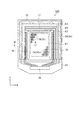
図2に示すように、有機EL装置100は、素子基板10を有している。素子基板10には、表示領域E0(図中、一点鎖線で表示)と、表示領域E0の外側に非表示領域E3とが設けられている。表示領域E0は、実表示領域E1(図中、二点鎖線で表示)と、実表示領域E1を囲むダミー領域E2とを有している。
As shown in FIG. 2, the
実表示領域E1には、発光画素としてのサブ画素18がマトリックス状に配置されている。サブ画素18は、前述したように発光素子としての有機EL素子30を備えており、スイッチング用トランジスター21及び駆動用トランジスター23の動作に伴って、青(B)、緑(G)、赤(R)のうちいずれかの色の発光が得られる構成となっている。
In the actual display area E1, sub-pixels 18 as light-emitting pixels are arranged in a matrix. The sub-pixel 18 includes the
本実施形態では、同色の発光が得られるサブ画素18が第1の方向に配列し、異なる色の発光が得られるサブ画素18が第1の方向に対して交差(直交)する第2の方向に配列した、所謂ストライプ方式のサブ画素18の配置となっている。以降、上記第1の方向をY方向とし、上記第2の方向をX方向として説明する。なお、素子基板10におけるサブ画素18の配置はストライプ方式に限定されず、モザイク方式、デルタ方式であってもよい。
In the present embodiment, the sub-pixels 18 that can emit light of the same color are arranged in the first direction, and the second direction in which the sub-pixels 18 that can emit light of different colors intersect (orthogonal) the first direction. The so-called stripe-
ダミー領域E2には、主として各サブ画素18の有機EL素子30を発光させるための周辺回路が設けられている。例えば、図2に示すように、X方向において実表示領域E1を挟んだ位置にY方向に延在して一対の走査線駆動回路16が設けられている。一対の走査線駆動回路16の間で実表示領域E1に沿った位置に検査回路17が設けられている。
The dummy area E2 is provided with a peripheral circuit mainly for causing the
素子基板10には、一対の走査線駆動回路16に沿ったY方向と検査回路17に沿ったX方向とに延在して、表示領域E0を囲むように配置された配線層24を有している。また、配線層24に重畳して配置され、配線層24と電気的に接続されたコンタクト部29とを有している。詳しくは後述するが、有機EL素子30の対向電極33は、複数の有機EL素子30すなわち複数のサブ画素18に亘って共通陰極として形成され、表示領域E0と非表示領域E3とに亘って形成されている。対向電極33は、非表示領域E3において上記コンタクト部29と接して形成されている。
The
素子基板10のY方向における一辺部(図中の下方の辺部)に、外部駆動回路との電気的な接続を図るためのフレキシブル回路基板(FPC)43が接続されている。FPC43には、FPC43の配線を介して素子基板10側の周辺回路と接続される駆動用IC44が実装されている。駆動用IC44は前述したデータ線駆動回路15を含むものであり、素子基板10側のデータ線13や電源線14は、FPC43を介して駆動用IC44に電気的に接続されている。共通陰極としての対向電極33もまた上記コンタクト部29、配線層24、FPC43を介して駆動用IC44に電気的に接続されている。
A flexible circuit board (FPC) 43 for electrical connection with an external drive circuit is connected to one side (the lower side in the figure) of the
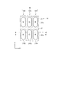
次に、図3を参照してサブ画素18の平面的な配置、とりわけ画素電極31の平面的な配置について説明する。図3に示すように、青(B)の発光が得られるサブ画素18B、緑(G)の発光が得られるサブ画素18G、赤(R)の発光が得られるサブ画素18RがX方向に順に配列している。同色の発光が得られるサブ画素18はY方向に配列している。X方向に配列した3つのサブ画素18B,18G,18Rを1つの画素19として表示がなされる構成になっている。
サブ画素18における画素電極31は略矩形状であって、長手方向がY方向に沿って配置されている。画素電極31を発光色に対応させて画素電極31B,31G,31Rと呼ぶこともある。各画素電極31B,31G,31Rの外縁を覆って絶縁層27が形成されている。これによって、各画素電極31B,31G,31R上に開口部27aが形成され、開口部27a内において画素電極31B,31G,31Rのそれぞれが露出している。開口部27aの平面形状もまた略矩形状となっている。
Next, the planar arrangement of the sub-pixels 18, particularly the planar arrangement of the
The
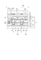
次に、有機EL装置100の構造について、図4及び図5を参照して説明する。図4は図3のA−A’線に沿った有機EL装置の構造を示す概略断面図、図5は図2のC−C’線に沿った有機EL装置の構造を示す概略断面図である。図4は実表示領域E1におけるサブ画素18の構造を示し、図5は非表示領域E3における封止構造を示すものである。
Next, the structure of the
図4に示すように、有機EL装置100は、基材11と、基材11上に順に形成された、画素回路20と、有機EL素子30と、複数の有機EL素子30を封止する封止層34とを含む素子基板10を備えている。また、素子基板10に対して透明樹脂層35を介して対向配置された対向基板41を備えている。
対向基板41は、例えばガラスなどの透明基板からなり、素子基板10のサブ画素18B,18G,18Rに対応して設けられた着色層36B,36G,36Rと、各着色層36B,36G,36Rを光学的に区分する遮光膜36Mとを有するカラーフィルター36を備えている。
サブ画素18B,18G,18Rの発光機能層32B,32G,32Rからの発光は、カラーフィルター36を透過して対向基板41側から取り出される。すなわち、有機EL装置100はトップエミッション型の発光装置である。
As shown in FIG. 4, the
The
Light emitted from the light emitting
基材11は、有機EL装置100がトップエミッション型のため、ガラスなどの透明基板や、シリコンやセラミックスなどの不透明な基板を用いることができる。以降、画素回路20に薄膜トランジスターを用いた場合を例に説明する。
基材11の表面を覆って第1層間絶縁膜11aが形成される。画素回路20における例えば駆動用トランジスター23の半導体層23aが第1層間絶縁膜11a上に形成される。半導体層23aを覆ってゲート絶縁膜として機能する第2層間絶縁膜11bが形成される。第2層間絶縁膜11bを介して半導体層23aのチャネル領域と対向する位置にゲート電極23gが形成される。ゲート電極23gを覆って第3層間絶縁膜11cが形成される。半導体層23aのソース領域23sとドレイン領域23dとにそれぞれ対応して、第2層間絶縁膜11bと第3層間絶縁膜11cとを貫通するコンタクトホールが形成される。これらのコンタクトホールを埋めるようにして導電膜が形成され、パターニングされて駆動用トランジスター23に接続される配線が形成される。図4では図示を省略したが、画素回路20におけるスイッチング用トランジスター21や蓄積容量22も同様に形成される。
第3層間絶縁膜11cを覆って第4層間絶縁膜11dが形成される。第4層間絶縁膜11dは、画素回路20の駆動用トランジスター23などを覆うことによって生じた表面の凹凸を無くすように平坦化処理が施される。また、後に画素電極31と駆動用トランジスター23とを電気的に接続させるためのコンタクトホールが第4層間絶縁膜11dを貫通して形成される。第1層間絶縁膜11a〜第4層間絶縁膜11dを構成する材料としては、例えばシリコンの酸化物や窒化物、あるいはシリコンの酸窒化物を用いることができる。
Since the
A first
A fourth
第4層間絶縁膜11dに形成されたコンタクトホールを埋めるように、第4層間絶縁膜11dを覆って導電膜が成膜され、この導電膜をパターニングすることによって画素電極31(31B,31G,31R)が形成される。画素電極31(31B,31G,31R)は、光反射性を有する例えばAl(アルミニウム)やAg(銀)、あるいはこれらの金属の合金を用いることができる。また、ITO(Indium Tin Oxide)などの透明導電膜を用いてもよい。透明導電膜を用いて画素電極31(31B,31G,31R)を形成した場合には、画素電極31(31B,31G,31R)と基材11との間に反射層を設ける。
A conductive film is formed to cover the fourth
各画素電極31B,31G,31Rの外縁部を覆って絶縁層27が形成され、これにより各画素電極31B,31G,31R上に開口部27aが形成される。絶縁層27は例えばシリコンの酸化物を用いて形成される。
絶縁層27上に隔壁28が形成される。隔壁28は例えばアクリル系の感光性樹脂を用いて、1μm〜2μm程度の高さで各画素電極31B,31G,31Rをそれぞれ区画するように形成される。
An insulating
A
本実施形態では、後述する発光機能層32(32B,32G,32R)が液相プロセスで形成されるため、隔壁28の表面には撥液処理が施され、隔壁28で囲まれた領域において露出した画素電極31B,31G,31Rの表面には親液処理が施される。なお、下層に絶縁層27、上層に隔壁28を有する所謂二層バンクの構成を採用することに限定されず、絶縁層27を除いて撥液性を有する隔壁28だけの構成としてもよい。
In the present embodiment, since the light emitting functional layer 32 (32B, 32G, 32R), which will be described later, is formed by a liquid phase process, the surface of the
隔壁28で区画された領域に発光機能層32(32B,32G,32R)がそれぞれ形成される。発光機能層32は、例えば、画素電極31側から、正孔注入層、正孔輸送層、有機発光層、電子輸送層が順に形成されたものである。本実施形態では、正孔注入層、正孔輸送層、有機発光層、電子輸送層ごとに、層構成材料を含む液体を用意し、隔壁28で区画された領域に当該液体を塗布して乾燥することにより、これらの層が積層された発光機能層32(32B,32G,32R)を形成している。当該液体を所定の領域に対して選択的に塗布する方法として液滴吐出法(インクジェット法)が用いられている。なお、発光機能層32(32B,32G,32R)は、上記液滴吐出法(インクジェット法)によって形成されることに限定されず、上記所定の領域に対応する開口部を有するマスクを用いた蒸着法により形成してもよい。
なお、発光機能層32Bから青(B)の発光が得られ、発光機能層32Gから緑(G)の発光が得られ、発光機能層32Rから赤(R)の発光が得られる。また、発光機能層32の層構成は、これに限定されず、キャリアである正孔や電子の移動を制御する中間層を含んでいてもよい。また、発光色に対応して有機発光層の層構成材料を変えるだけでなく、発光色に対応して正孔注入層や正孔輸送層などの構成を異ならせてもよい。
The light emitting functional layers 32 (32B, 32G, 32R) are formed in regions partitioned by the
Note that blue (B) light is obtained from the light emitting
発光機能層32(32B,32G,32R)と隔壁28とを覆って共通陰極としての対向電極33が形成される。対向電極33は、例えばMgとAgとの合金を光透過性が得られる程度の膜厚(例えば10nm〜30nm)で成膜することによって形成される。これによって、複数の有機EL素子30ができあがる。
A
次に、水や酸素などが浸入しないように複数の有機EL素子30を覆う封止層34が形成される。本実施形態の封止層34は、対向電極33側から順に、第1無機封止層34a、緩衝層34b、第2無機封止層34cが積層されたものである。
第1無機封止層34a及び第2無機封止層34cとしては、光透過性を有すると共に優れたガスバリア性を有する無機材料である例えば酸窒化シリコン(SiON)などを用いることが好ましい。
Next, a
As the first
無機封止層の形成方法としては、蒸着法やスパッタ法を挙げることができる。無機封止層の膜厚を厚くすることで高いガスバリア性を実現できるが、その一方で膨張や収縮によってクラックが生じ易い。したがって、200nm〜400nm程度の膜厚に制御することが好ましく、本実施形態では緩衝層34bを挟んで無機封止層を重ねることで高いガスバリア性を実現している。
Examples of the method for forming the inorganic sealing layer include a vapor deposition method and a sputtering method. Although a high gas barrier property can be realized by increasing the thickness of the inorganic sealing layer, cracks are likely to occur due to expansion and contraction. Therefore, it is preferable to control the film thickness to about 200 nm to 400 nm. In this embodiment, a high gas barrier property is realized by overlapping the inorganic sealing layer with the
緩衝層34bは、熱安定性に優れた例えばエポキシ系樹脂を用いることができる。また、有機材料からなる緩衝層34bをスクリーンなどの印刷法や定量吐出法などにより塗布形成すれば、緩衝層34bの表面を平坦化することができる。つまり、緩衝層34bは第1無機封止層34aの表面の凹凸を緩和する平坦化層としても機能させることができる。
For the
素子基板10と対向基板41とは、間隔を置いて対向配置され、当該間隔に透明樹脂が充填されて透明樹脂層35が構成される。透明樹脂としては、例えばウレタン系、アクリル系、エポキシ系、ポリオレフィン系などの樹脂を挙げることができる。
The
図5に示すように、非表示領域E3において、基材11の第3層間絶縁膜11c上に配線層24が設けられている。第4層間絶縁膜11d上にコンタクト部29が設けられている。配線層24とコンタクト部29とは、第4層間絶縁膜11dに形成されたコンタクトホールを介して電気的に接続されている。なお、配線層24及びコンタクト部29の構成はこれに限定されず、例えば第4層間絶縁膜11d上に配線層24を形成し、配線層24に接するようにコンタクト部29を形成してもよい。あるいは、第4層間絶縁膜11dが基材11よりも狭い範囲に形成され、第4層間絶縁膜11dの外縁(平面視した際の第4層間絶縁膜11dの外縁と基材11の外縁の間の領域)で配線層24に接するようにコンタクト部29を形成してもよい。
共通陰極としての対向電極33は表示領域E0と非表示領域E3とに亘って形成されている。非表示領域E3では、対向電極33はコンタクト部29と第4層間絶縁膜11dとに接するように形成されている。
封止層34のうち、第1無機封止層34aと第2無機封止層34cは、非表示領域E3において互いに接すると共に、対向電極33と重なるように形成されている。緩衝層34bは、少なくとも表示領域E0と重なるように第1無機封止層34aに積層形成されている。
As shown in FIG. 5, the
The
Of the
複数の有機EL素子30が設けられた素子基板10と、カラーフィルター36を備えた対向基板41とを透明樹脂層35を介して対向配置して接着するにあたり、非表示領域E3には表示領域E0を囲むようにダム材42が設けられている。ダム材42は例えばエポキシ系樹脂を主体とする熱硬化型の接着剤を用いることができる。
When the
<発光装置の製造方法>
次に、本実施形態の発光装置の製造方法としての有機EL装置100の製造方法について、図6及び図7を参照して説明する。図6は第1実施形態の有機EL装置の製造方法を示すフローチャート、図7(a)〜(e)は第1実施形態の有機EL装置の製造方法を示す概略断面図である。なお、図7は図2のC−C’線に沿った素子基板10の断面図に相当するものである。
<Method for manufacturing light emitting device>
Next, a manufacturing method of the
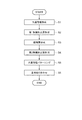
図6に示すように、本実施形態の発光装置の製造方法としての有機EL装置100の製造方法は、共通陰極形成工程(ステップS1)と、第1無機封止層形成工程(ステップS2)と、緩衝層形成工程(ステップS3)と、第2無機封止層形成工程(ステップS4)と、共通陰極パターニング工程(ステップS5)と、素子基板10と対向基板41とを貼り合わせる基板貼り合わせ工程(ステップS6)とを備えている。
なお、素子基板10において、画素回路20を形成する工程や、有機EL素子30のうち画素電極31、発光機能層32を形成する工程は、前述したように公知の方法を用いることができる。したがって、本実施形態では、本願の特徴部分である共通陰極形成工程以降について説明する。
As shown in FIG. 6, the manufacturing method of the
In the
図6の共通陰極形成工程(ステップS1)では、図7(a)に示すように、共通陰極としての対向電極33を表示領域E0と非表示領域E3とに亘って形成する。対向電極33は、例えばMgとAgとの合金(MgAg)を蒸着法やスパッタ法などを用いて、表示領域E0では発光機能層32と隔壁28とに接して覆うように形成する。非表示領域E3では少なくともコンタクト部29に接して覆うように形成する。対向電極33は膜厚を10nm〜30nmと薄く成膜することにより、導電性に加えて光透過性が付与される。そして、ステップS2へ進む。
In the common cathode forming step (step S1) in FIG. 6, as shown in FIG. 7A, the
図6の第1無機封止層形成工程(ステップS2)では、図7(b)に示すように、第1無機封止層34aを表示領域E0と非表示領域E3とに亘って形成する。第1無機封止層34aは、例えばSiON(酸窒化シリコン)を蒸着法やスパッタ法などを用いて対向電極33に接して覆うように形成する。ただし、非表示領域E3では、対向電極33を介してコンタクト部29と重なると共に、対向電極33の外縁が露出するように形成する。つまり、対向電極33が形成された領域よりも内側に第1無機封止層34aを形成する。このような第1無機封止層34aの選択的な形成は、例えば、第1無機封止層34aが形成される領域に対応した開口を有するマスクを用いて蒸着またはスパッタすることによって実現できる。第1無機封止層34aの膜厚は200nm〜400nmである。そして、ステップS3へ進む。
In the first inorganic sealing layer forming step (step S2) in FIG. 6, as shown in FIG. 7B, the first
図6の緩衝層形成工程(ステップS3)では、図7(c)に示すように、緩衝層34bを少なくとも表示領域E0に亘って形成する。緩衝層34bは、例えば、光透過性を有するエポキシ系樹脂(モノマー、オリゴマーと硬化剤とを含む)をスクリーンなどの印刷法や定量吐出法などにより、第1無機封止層34aに接して覆うように形成する。第1無機封止層34aにスクリーンなどの印刷手段が触れない点で、定量吐出法を採用することが好ましい。例えば、上記エポキシ系樹脂に溶媒を加えて吐出可能な程度の粘度に調整された溶液をノズルから表示領域E0に満遍なく吐出し、塗布された溶液を乾燥させて緩衝層34bを形成する。溶液を乾燥する過程でレベリングされ、乾燥後に表面が比較的に平坦な緩衝層34bを得ることができる。緩衝層34bの膜厚は、異物などが混入した場合に、この後に形成される第2無機封止層34cの形成に影響を及ぼさないように、1μm〜3μmとすることが好ましい。そして、ステップS4へ進む。
In the buffer layer forming step (step S3) of FIG. 6, as shown in FIG. 7C, the
図6の第2無機封止層形成工程(ステップS4)では、図7(d)に示すように、第2無機封止層34cを表示領域E0と非表示領域E3とに亘って形成する。第2無機封止層34cは、第1無機封止層34aと同じ材料を用いて形成することが望ましく、SiONが好ましい。表示領域E0では緩衝層34bに接して覆うように形成し、非表示領域E3では第1無機封止層34aに接するように形成する。第2無機封止層34cは、第1無機封止層34aが形成された領域と同じか、それよりもやや内側に形成する。このような第2無機封止層34cの選択的な形成もまたマスクを用いて蒸着またはスパッタすることによって実現できる。第2無機封止層34cの膜厚は200nm〜400nmである。これにより、封止層34ができあがる。ステップS2〜ステップS4が封止層34の形成工程に相当する。そして、ステップS5へ進む。
In the second inorganic sealing layer forming step (step S4) in FIG. 6, as shown in FIG. 7D, the second
図6の共通陰極パターニング工程(ステップS5)では、図7(e)に示すように、封止層34をマスクとして共通陰極である対向電極33をエッチングしてパターニングする。対向電極33をエッチングする方法としては、酸素を含む処理ガスを用いたドライエッチングを挙げることができる。封止層34をマスクとしたドライエッチングを施すことにより、封止層34よりも膜厚が薄い対向電極33が優先的にエッチングされ、非表示領域E3において対向電極33の端部33eと封止層34の端部34eとが揃った断面形状を実現できる。また、このとき、封止層34で覆われていない、対向電極33の端部33eは、処理ガスに含まれた酸素によって不動態化される。対向電極33と接するコンタクト部29は、対向電極33の端部33eよりも内側(表示領域E0側)に位置しているので、酸素によって不動態化されることはない。そして、ステップS6へ進む。
In the common cathode patterning step (step S5) of FIG. 6, as shown in FIG. 7E, the
図6の基板貼り合わせ工程(ステップS6)では、図5に示すように、複数の有機EL素子30を封止する封止層34が形成された素子基板10と、カラーフィルター36を有する対向基板41とを透明樹脂層35を介して貼り合わせる。貼り合わせ方法としては、素子基板10または対向基板41の非表示領域E3に例えば熱硬化型の接着剤であるダム材42を配置し、ダム材42が配置された基板のダム材42より内側に所定量の透明樹脂を塗布する。そして、両基板を所定の位置で対向配置して圧着し、ダム材42を加熱硬化させる。これによって、素子基板10と対向基板41との間に透明樹脂層35が形成される。ダム材42を非表示領域E3に配置することにより、圧着によって透明樹脂が両基板から外側にはみ出ることを防止すると共に、両基板を所定の間隔をおいて接着することができる。ダム材42には、所定の間隔をおいて両基板を配置させるためのギャップ材を含むことが望ましい。
In the substrate bonding step (step S6) in FIG. 6, as shown in FIG. 5, the
上記第1実施形態によれば、以下の効果が得られる。
(1)有機EL装置100及びその製造方法によれば、非表示領域E3において封止層34は対向電極33の端部33eを覆って形成されず、結果的に対向電極33の形成領域と同じ領域またはそれよりも内側(表示領域E0側)に形成される。したがって、対向電極33の端部33eを覆うように封止層34を形成する場合に比べて、非表示領域E3のX方向及びY方向の幅を狭く(小さく)することができる。つまり、発光寿命における信頼性を確保しつつ、小型な発光装置としての有機EL装置100を提供できる。
(2)対向電極33は封止層34をマスクとしてドライエッチングすることによりパターニングされる。これにより、封止層34で覆われていない対向電極33の端部33eが処理ガスに含まれた酸素により不動態化される。この後、対向電極33の端部33eが水や酸素に触れたとしても不動態化されているので、水や酸素が表示領域E0に浸入することを抑制できる。また、対向電極33の不動態化された端部33eよりも内側(表示領域E0側)にコンタクト部29が配置されているので、水や酸素の表示領域E0への浸入をより確実に抑制することができる。
(3)複数の有機EL素子30を覆って封止する封止層34は、対向電極33側から第1無機封止層34a、緩衝層34b、第2無機封止層34cの積層構造となっている。したがって、封止層34を単純に無機材料からなる厚膜とする場合に比べて、熱膨張・収縮によるクラックや剥がれなどの不具合を低減し、確実に水や酸素などの浸入を抑制できる。また、緩衝層34bは塗布法により有機材料を用いて形成されている。したがって、複数の有機EL素子30の影響で第1無機封止層34aの表面に凹凸が生じたとしても、これを緩和する平坦化層として緩衝層34bを機能させることができる。
(4)素子基板10と対向基板41とは透明樹脂層35を介してダム材42により貼り合わせられる。したがって、透明樹脂が両基板から外側にはみ出ることを防止することができる。また、素子基板10と対向基板41とを強力に接着できることから、複数の有機EL素子30を確実に封止することができる。
(5)素子基板10に対向配置される対向基板41には、サブ画素18B,18G,18Rにそれぞれ対応した着色層36B,36G,36Rを有するカラーフィルター36が設けられている。発光機能層32B,32G,32Rから発した光は着色層36B,36G,36Rを透過する。したがって、高い色純度でフルカラー表示が可能な有機EL装置100を提供できる。
According to the first embodiment, the following effects can be obtained.
(1) According to the
(2) The
(3) The
(4) The
(5) A
(第2実施形態)
<発光装置>
次に、第2実施形態の発光装置としての有機EL装置について、図8及び図9を参照して説明する。図8は第2実施形態の有機EL装置の構造を示す概略断面図、図9(a)及び(b)は第2実施形態の有機EL装置の非表示領域の構造を示す概略断面図である。なお、第2実施形態の発光装置としての有機EL装置は、第1実施形態の有機EL装置100に対して素子基板10の構成を異ならせたものであり、図8は図3のA−A’線に沿った断面図に相当し、図9(a)及び(b)は図2のC−C’線に沿った断面図に相当するものである。したがって、第1実施形態と同じ構成には同じ符号を付して詳細の説明は省略する。また、図8及び図9では、基材11上に形成されている画素回路20の駆動用トランジスター23などの表示を省略した。
(Second Embodiment)
<Light emitting device>
Next, an organic EL device as a light emitting device of the second embodiment will be described with reference to FIGS. FIG. 8 is a schematic cross-sectional view showing the structure of the organic EL device of the second embodiment, and FIGS. 9A and 9B are schematic cross-sectional views showing the structure of the non-display region of the organic EL device of the second embodiment. . The organic EL device as the light emitting device of the second embodiment is different from the
図8に示すように、本実施形態の発光装置としての有機EL装置200は、基材11と、基材11上に順に形成された反射層25、透明層26、画素電極31B,31G,31R、発光機能層32、共通陰極としての対向電極33を有する。また、対向電極33を覆う封止層34と、封止層34上に形成されたカラーフィルター36とを有する。さらに、カラーフィルター36を保護するために、素子基板10に透明樹脂層45を介して配置された対向基板41を有する。本実施形態の素子基板10は基材11からカラーフィルター36までを含むものである。
As shown in FIG. 8, the
サブ画素18B,18G,18Rに対応して設けられた画素電極31B,31G,31Rは、例えばITOなどの透明導電膜からなり、互いに膜厚が異なっている。青(B)、緑(G)、赤(R)の順に膜厚が厚くなっている。
発光機能層32はサブ画素18B,18G,18Rに跨って共通に形成されており、白色発光が得られる構成となっている。
発光機能層32を覆う対向電極33は、例えばMgAg合金からなり、光透過性と光反射性とを兼ね備えるように膜厚が制御されている。
本実施形態の有機EL装置200は、反射層25と対向電極33との間で光共振器が構成されている。サブ画素18B,18G,18Rごとの画素電極31B,31G,31Rの膜厚が異なることにより、それぞれの光共振器における光学的な距離が異なっている。これにより、サブ画素18B,18G,18Rのそれぞれにおいて各色に対応した共振波長の光が得られる構成となっている。
カラーフィルター36の各着色層36B,36G,36Rは封止層34上に直接形成されている。
各サブ画素18B,18G,18Rの光共振器から発せられた共振光は、各着色層36B,36G,36Rを透過して透明な対向基板41側から射出される。カラーフィルター36が封止層34上に形成されているため、サブ画素18B,18G,18R間での光漏れによる混色が低減される。このようなサブ画素18B,18G,18Rの構造は、サブ画素18B,18G,18Rの平面的な大きさが小さくなればなるほど混色を効果的に低減できる。
The
The light emitting
The
In the
The colored layers 36B, 36G, and 36R of the
Resonant light emitted from the optical resonators of the sub-pixels 18B, 18G, and 18R passes through the
図9(a)に示すように、非表示領域E3では、対向電極33はコンタクト部29に接して覆うように形成されている。封止層34のうち第1無機封止層34aは対向電極33に接して覆うように形成されている。ただし、対向電極33の端部33eは第1無機封止層34aによって覆われていない。第1無機封止層34aに対して緩衝層34bを介して形成された第2無機封止層34cは、非表示領域E3において第1無機封止層34aと接して積層されている。
素子基板10と対向基板41とは、非表示領域E3に配置されたダム材42によって貼り合わされている。
As shown in FIG. 9A, in the non-display area E <b> 3, the
The
図9(a)では、対向電極33の端部33eと封止層34の端部34eとが揃った断面形状となっている。また、ダム材42の端に対しても揃った断面形状となっている。言い換えれば、封止層34は対向電極33の端部33eを覆う必要がなく、ダム材42もまた対向電極33の端部33eや封止層34の端部34eを覆う必要がないので、これらの端部33e,34eを覆うように形成する場合に比べて、非表示領域E3の幅を小さくできる。
In FIG. 9A, the
なお、対向電極33の端部33eと封止層34の端部34eとを断面形状において必ず揃える必要はなく、例えば、図9(b)に示すように、対向電極33が形成された領域よりも内側(表示領域E0側)に封止層34を形成すればよく、対向電極33の端部33eと封止層34の端部34eとの間に段差が生じてもよい。
また、素子基板10と対向基板41とを接着するダム材42は、対向電極33の端部33eに対してダム材42の端を揃えて配置する必要はなく、対向電極33の端部33eよりも表示領域E0側にダム材42を配置してもよい。
本実施形態においても、第1実施形態と同様に封止層34で覆われていない対向電極33の部分(端部33eを含む)は、不動態化されている。詳しくは、以降の有機EL装置200の製造方法において説明する。
The
In addition, the
Also in the present embodiment, the portion of the counter electrode 33 (including the
<発光装置の製造方法>
第2実施形態の発光装置の製造方法としての有機EL装置200の製造方法について、図10〜図12を参照して説明する。図10は第2実施形態の有機EL装置の製造方法を示すフローチャート、図11はマザー基板の構成を示す概略平面図、図12(a)〜(e)は第2実施形態の有機EL装置の製造方法を示す概略断面図である。
<Method for manufacturing light emitting device>
A manufacturing method of the
図10に示すように、本実施形態の有機EL装置200の製造方法は、共通陰極形成工程(ステップS11)と、封止層形成工程(ステップS12)と、共通陰極パターニング工程(ステップS13)と、カラーフィルター形成工程(ステップS14)と、基板貼り合わせ工程(ステップS15)と、ダイシング工程(ステップS16)とを備えている。
As shown in FIG. 10, the manufacturing method of the
本実施形態では、図11に示すように、素子基板10の基材11が設計上、複数面付けされたマザー基板10Wを用いて、有機EL装置200を製造するものである。マザー基板10Wには、オリフラのカット面が延在する方向をX方向として、X方向とY方向とに複数の基材11が所定の間隔を置いて面付けされている。基材11上に前述した素子基板10の各構成を形成し、個々の素子基板10に対して対向基板41をそれぞれ貼り合わせる。そして、X方向とY方向とに延在する上記間隔に設定されたスクライブライン(仮想切断線)SLに沿ってダイシングすることにより、個々の有機EL装置200が取り出される。
In the present embodiment, as shown in FIG. 11, the
本実施形態の有機EL装置200がトップエミッション方式であることから、マザー基板10Wは、透明な例えば石英や無アルカリガラスなどの基板や、不透明なシリコンなどの基板を用いることができる。本実施形態では、マザー基板10Wとして石英基板を用い、高温プロセスを使用して画素回路20のトランジスター等をマザー基板10W上に形成している。このような画素回路20の形成方法は、公知の方法を採用することができる。
Since the
なお、図12(a)〜(e)は、マザー基板10WのX方向において隣り合う基材11の概略断面図を示している。また、図12(a)〜(e)は、素子基板10側における画素回路20や画素電極31等の表示を省略して、本実施形態に係る共通陰極形成工程以降の内容を分かり易く表示したものである。
12A to 12E are schematic cross-sectional views of the
具体的には、図10の共通陰極形成工程(ステップS11)では、図12(a)に示すように、共通陰極としての対向電極33を、複数の基材11の絶縁層27とコンタクト部29と発光機能層32とを覆うように、マザー基板10Wの全面に亘って形成する。対向電極33は、前述したように、例えばMgAg合金を用いて蒸着あるいはスパッタすることにより形成され、その厚みは光透過性と光反射性とを兼ね備えるように、例えば10nm〜30nmとされている。そして、ステップS12へ進む。
Specifically, in the common cathode forming step (step S11) of FIG. 10, as shown in FIG. 12A, the
図10の封止層形成工程(ステップS12)では、図12(a)に示すように、各基材11に対応して、スクライブラインSLを挟んで間隔をおいて封止層34を形成する。本実施形態の封止層形成工程は、第1無機封止層形成工程、緩衝層形成工程、第2無機封止層形成工程を含むものであって、基本的に第1実施形態のステップS2〜ステップS4と同じであるため、詳細の説明は省略する。そして、ステップS13へ進む。
In the sealing layer forming step (step S12) of FIG. 10, as shown in FIG. 12A, the
図10の共通陰極パターニング工程(ステップS13)では、図12(b)に示すように、封止層34をマスクとして対向電極33をエッチングしてパターニングする。エッチング方法は、第1実施形態のステップS5と同様にして酸素を含む処理ガスを用いたドライエッチング法を採用することができる。したがって、ドライエッチング後に封止層34で覆われていない対向電極33の部分(端部33eを含む)が酸素と反応して不動態化される。そして、ステップS14へ進む。
In the common cathode patterning step (step S13) in FIG. 10, as shown in FIG. 12B, the
図10のカラーフィルター形成工程(ステップS14)では、図12(c)に示すように、封止層34上にカラーフィルター36を形成する。カラーフィルター36の形成方法は、各着色層36B,36G,36Rに対応した色材を含む感光性樹脂材料をスピンコート法などの方法を用いてマザー基板10Wに塗布し、これを露光・現像・乾燥することで、着色層36B,36G,36Rをそれぞれ形成する。着色層36B,36G,36Rの膜厚はおよそ2μm程度である。そして、ステップS15へ進む。
In the color filter forming step (step S14) of FIG. 10, the
図10の基板貼り合わせ工程(ステップS15)では、図12(d)に示すように、マザー基板10Wの基材11ごとにダム材42を配置する。配置されたダム材42の内側に所定量の透明樹脂材料を塗布して、対向基板41を貼り合わせる。本実施形態では、マザー基板10Wの基材11ごとにダム材42を所定の位置(表示領域E0を囲む所定の位置)に配置する。そして、基材11ごとに対向配置された対向基板41を基材11側に押圧して加熱することによりダム材42を硬化させて、マザー基板10Wに複数の対向基板41を貼り合わせる。これにより、マザー基板10Wと対向基板41との間に透明樹脂材料が充填されて透明樹脂層45が構成される。そして、ステップS16へ進む。
In the substrate bonding step (step S15) in FIG. 10, as shown in FIG. 12 (d), the
図10のダイシング工程(ステップS16)では、図12(e)に示すように、スクライブラインSLに沿ってダイシングしてマザー基板10Wを切断することにより、個々の有機EL装置200を取り出す。ダイシングは、マザー基板10Wに面付けされた基材11の周囲に設けられた間隔を切りしろとして行われる。したがって、ダイシングブレードによって、対向電極33や封止層34が切断されることはない。
In the dicing step (step S16) in FIG. 10, as shown in FIG. 12E, the individual
なお、本実施形態では、マザー基板10Wに面付けされた基材11のそれぞれに個片の対向基板41を貼り合わせたが、対向基板41が面付けされたマザー対向基板とマザー基板10Wとを貼り合わせて、双方を切断して有機EL装置200を取り出す方法を採用してもよい。また、これらの基板の切断は、ダイシングに限定されず、超鋼チップによるスジ入れスクライブや、レーザー光を照射して切断するレーザースクライブを用いたり、これらの切断方法を組み合わせて用いたりすることもできる。
In this embodiment, the
上記第2実施形態の有機EL装置200及びその製造方法によれば、上記第1実施形態の効果(1)、(2)、(3)と同様な効果に加えて、以下の効果が得られる。
(6)有機EL装置200は、素子基板10側においてサブ画素18B,18G,18Rごとに光共振器と着色層36B,36G,36Rとを備えている。したがって、着色層36B,36G,36Rを対向基板41側に設けた場合に比べて、有機EL素子30に対してカラーフィルター36が近づいて配置され、サブ画素18B,18G,18R間の光漏れによる混色が低減され優れた表示品質を有する小型な有機EL装置200を提供できる。
(7)ダイシング工程(ステップS16)では、マザー基板10Wに面付けされた基材11の周囲に設けられた間隔を切りしろとしてダイシングが行われる。したがって、対向電極33や封止層34が切断されて損傷したり、基材11から剥がれたりすることがないので、高い信頼性を実現できる。
(8)共通陰極パターニング工程(ステップS13)において、封止層34で覆われていない対向電極33の部分(端部33eを含む)は不動態化されており、ダイシング工程(ステップS16)において水と接触しても、対向電極33が水の影響を受け難い。
According to the
(6) The
(7) In the dicing step (step S16), dicing is performed with a gap provided around the
(8) In the common cathode patterning step (step S13), the portion of the counter electrode 33 (including the
(第3実施形態)
<電子機器>
次に、本実施形態の電子機器について図13、図14を参照して説明する。図13は電子機器としてのテレビを示す概略図、図14は電子機器としてのヘッドマウントディスプレイを示す斜視図である。
図13に示すように、本実施形態の電子機器としてのテレビ(TV)500は、表示部501に上記実施形態の有機EL装置100が用いられている。したがって、発光寿命において高い信頼性を有すると共に、非表示領域E3の幅が小さいので、同じ画面サイズなら従来に比べてより小型なTV500を提供できる。また、液晶表示装置を表示部501に採用する場合に比べて、照明装置が不要になることからより薄型のTV500を実現できる。
(Third embodiment)
<Electronic equipment>
Next, the electronic apparatus of this embodiment will be described with reference to FIGS. FIG. 13 is a schematic view showing a television as an electronic apparatus, and FIG. 14 is a perspective view showing a head-mounted display as an electronic apparatus.
As shown in FIG. 13, a television (TV) 500 as an electronic apparatus according to the present embodiment uses the
図14に示すように、本実施形態の電子機器としてのヘッドマウントディスプレイ1000は、左右の目に対応して設けられた2つの表示部1001を有している。観察者Mはヘッドマイントディスプレイ1000を眼鏡のように頭部に装着することにより、表示部1001に表示された文字や画像などを見ることができる。例えば、左右の表示部1001に視差を考慮した画像を表示すれば、立体的な映像を見て楽しむこともできる。
表示部1001には、上述した有機EL装置200が搭載されている。したがって、発光寿命において高い信頼性を有すると共に、従来に比べてより小型で軽量なヘッドマウントディスプレイ1000を提供することができる。
ヘッドマウントディスプレイ1000は、2つの表示部1001を有することに限定されず、左右のいずれかに対応させた1つの表示部1001を備える構成としてもよい。
As shown in FIG. 14, the head mounted
The above-described
The head mounted
なお、上記有機EL装置100または有機EL装置200が搭載された電子機器は、TV500やヘッドマウントディスプレイ1000に限定されない。例えば、パーソナルコンピューターや携帯型情報端末、ナビゲーター、ビューワー、ヘッドアップディスプレイなどの表示部を有する電子機器が挙げられる。
The electronic device on which the
本発明は、上記した実施形態に限られるものではなく、請求の範囲および明細書全体から読み取れる発明の要旨あるいは思想に反しない範囲で適宜変更可能であり、そのような変更を伴う発光装置および該発光装置の製造方法ならびに該発光装置を適用する電子機器もまた本発明の技術的範囲に含まれるものである。上記実施形態以外にも様々な変形例が考えられる。以下、変形例を挙げて説明する。 The present invention is not limited to the above-described embodiment, and can be appropriately changed without departing from the gist or concept of the invention that can be read from the claims and the entire specification. A manufacturing method of a light emitting device and an electronic apparatus to which the light emitting device is applied are also included in the technical scope of the present invention. Various modifications other than the above embodiment are conceivable. Hereinafter, a modification will be described.
(変形例1)上記第1実施形態の緩衝層形成工程(ステップS3)において、塗布法を用いて緩衝層34bを形成する前に、第1無機封止層34aが形成された基材11に対して、酸素を処理ガスとするプラズマ処理を施してもよい。これにより、第1無機封止層34aの表面がクリーニングされて緩衝層34bとの密着性が高まる。また、プラズマ処理によって第1無機封止層34aに覆われていない対向電極33の部分を不動態化することができる。言い換えれば、封止層34で覆われていない対向電極33の部分を不動態化する工程は、ドライエッチングを用いる共通陰極パターニング工程に限定されない。例えば、環境条件にもよるが対向電極33の露出した部分が大気中の酸素と反応して不動態化されることもある。
(Modification 1) In the buffer layer forming step (step S3) of the first embodiment, before forming the
(変形例2)上記第1実施形態及び上記第2実施形態において、封止層34の緩衝層34bを有機材料を用いて構成したが、これに限定されない。封止層34のうち第1無機封止層34a、第2無機封止層34cに与えられる製造上のストレスに対して、これを緩和可能な物理的特性(例えば弾性率)を備えていれば、無機材料を用いて緩衝層34bを構成することもできる。
(Modification 2) In the first embodiment and the second embodiment, the
(変形例3)上記第1実施形態及び上記第2実施形態において、共通陰極パターニング工程における対向電極33のパターニング方法は、封止層34をマスクとしたドライエッチングに限定されない。例えば、封止層34を覆ってエッチング用レジストパターンを形成し、ウェットエッチングによって対向電極33をパターニングしてもよい。そうすると、エッチング後の対向電極33の端部33eと封止層34の端部34eとが必ずしも揃わない断面形状となることもある。
(Modification 3) In the first embodiment and the second embodiment, the patterning method of the
(変形例4)上記第1実施形態の有機EL装置100において、配線層24と共通陰極としての対向電極33との電気的な接続を図るコンタクト部29は、X方向またはY方向に連続して設けられていることに限定されない。例えば、基材11上において配線層24と対向電極33との間で島状に複数設けられていてもよい。
(Modification 4) In the
(変形例5)上記第1実施形態及び第2実施形態において、素子基板10と対向基板41とをダム材42を介して接着したが、これに限定されない。例えば、透明樹脂層35(透明樹脂層45)に接着性を持たせてダム材42を設けずに素子基板10と対向基板41とを接着してもよい。これによれば、ダム材42を非表示領域E3に配置するときの位置精度を考慮して、非表示領域E3のX方向及びY方向における幅に余裕を持たせる必要がなくなる。したがって、非表示領域E3の幅を狭めて、より小型な有機EL装置100及び有機EL装置200を提供できる。透明樹脂層35(透明樹脂層45)は、少なくとも表示領域E0と重なって形成されていればよく、必ずしも対向電極33の端部33eや封止層34の端部34eを覆う必要はない。
(Modification 5) In the first embodiment and the second embodiment, the
(変形例6)上記第1実施形態の有機EL装置100及び上記第2実施形態の有機EL装置200において、実表示領域E1に設けられる発光画素は、青(B)、緑(G)、赤(R)の発光に対応したサブ画素18B,18G,18Rに限定されない。例えば、上記3色以外の黄(Y)を発光するサブ画素18Yを備えてもよい。これにより、色再現性をさらに高めることが可能となる。
(Modification 6) In the
(変形例7)上記第1実施形態の封止構造を適用可能な発光装置は、トップエミッション型の有機EL装置100,200に限定されない。例えば、対向電極33を反射層とし、画素電極31と基材11との間に半透過反射層を設け、発光機能層32からの発光を基材11側から取り出すボトムエミッション型の有機EL装置にも適用することができる。
(Modification 7) The light emitting device to which the sealing structure of the first embodiment can be applied is not limited to the top emission type
10…素子基板、10W…マザー基板、11…基板としての基材、24…配線層、29…コンタクト部、30…発光素子としての有機EL素子、31,31B,31G,31R…陽極としての画素電極、32…有機発光層を含む機能層としての発光機能層、33…共通陰極としての対向電極、34…封止層、34a…第1無機封止層、34b…緩衝層、34c…第2無機封止層、35…透明樹脂層、36…カラーフィルター、36B,36G,36R…着色層、41…対向基板、42…ダム材、100,200…発光装置としての有機EL装置、500…電子機器としてのテレビ(TV)、1000…電子機器としてのヘッドマウントディスプレイ、SL…スクライブライン。
DESCRIPTION OF
Claims (19)
前記基板上に形成された、陽極と陰極との間に有機発光層が含まれる機能層を有する複数の発光素子と、
前記複数の発光素子を覆うように形成された封止層と、を備え、
前記陰極は前記複数の発光素子に亘る共通陰極として形成され、
前記封止層は、前記共通陰極の形成領域と同じもしくは前記共通陰極の形成領域より内側において前記共通陰極を覆うように形成されており、
前記基板と前記共通陰極との間に形成された配線層と、
前記配線層と前記共通陰極との間に形成され、前記封止層で覆われた部分の前記共通陰極に接し、前記共通陰極と前記配線層とを電気的に接続させるコンタクト部と、をさらに備えていることを特徴とする発光装置。 A substrate,
A plurality of light-emitting elements formed on the substrate and having a functional layer including an organic light-emitting layer between an anode and a cathode;
A sealing layer formed to cover the plurality of light emitting elements,
The cathode is formed as a common cathode across the plurality of light emitting elements,
The sealing layer is formed so as to cover the common cathode in the same area as the common cathode formation area or inside the common cathode formation area,
A wiring layer formed between the substrate and the common cathode;
A contact portion formed between the wiring layer and the common cathode and in contact with the portion of the common cathode covered with the sealing layer to electrically connect the common cathode and the wiring layer; A light-emitting device comprising:
前記ダム材は前記封止層の外縁と平面視で重なる位置に設けられていることを特徴とする請求項2に記載の発光装置。 A dam material that prevents the transparent resin layer from protruding outside the counter substrate,
The light emitting device according to claim 2, wherein the dam material is provided at a position overlapping the outer edge of the sealing layer in plan view .
前記ダム材は前記コンタクト部と平面視で重なる位置に設けられていることを特徴とする請求項2に記載の発光装置。 A dam material that prevents the transparent resin layer from protruding outside the counter substrate,
The light emitting device according to claim 2, wherein the dam material is provided at a position overlapping the contact portion in plan view .
前記基板上に形成された、陽極と陰極との間に有機発光層が含まれる機能層を有する複数の発光素子と、
前記複数の発光素子を覆うように形成された封止層と、
前記基板の前記封止層に対して透明樹脂層を介して対向配置された対向基板と、
前記透明樹脂層が前記対向基板から外側にはみ出すことを防止するダム材と、を有し、
前記陰極は前記複数の発光素子に亘る共通陰極として形成され、
前記封止層は、前記共通陰極の形成領域と同じもしくは前記共通陰極の形成領域より内側において前記共通陰極を覆うように形成されており、
前記基板上の前記複数の発光素子の形成領域の外側において、前記ダム材の端部と前記共通陰極の端部とが平面視で重なるように形成されていることを特徴とする発光装置。 A substrate,
A plurality of light-emitting elements formed on the substrate and having a functional layer including an organic light-emitting layer between an anode and a cathode;
A sealing layer formed to cover the plurality of light emitting elements;
A counter substrate disposed opposite to the sealing layer of the substrate via a transparent resin layer;
A dam material that prevents the transparent resin layer from protruding outside the counter substrate; and
The cathode is formed as a common cathode across the plurality of light emitting elements,
The sealing layer is formed so as to cover the common cathode in the same area as the common cathode formation area or inside the common cathode formation area,
The light emitting device, wherein an end portion of the dam material and an end portion of the common cathode are formed so as to overlap each other in a plan view outside a formation region of the plurality of light emitting elements on the substrate .
前記配線層と前記共通陰極との間に形成され、前記封止層で覆われた部分の前記共通陰極に接し、前記共通陰極と前記配線層とを電気的に接続させるコンタクト部と、をさらに備えていることを特徴とする請求項5に記載の発光装置。 A wiring layer formed between the substrate and the common cathode;
A contact portion formed between the wiring layer and the common cathode and in contact with the portion of the common cathode covered with the sealing layer to electrically connect the common cathode and the wiring layer; The light emitting device according to claim 5, further comprising:
前記基板上に形成された、陽極と陰極との間に有機発光層が含まれる機能層を有する複数の発光素子と、
前記複数の発光素子を覆うように形成された封止層と、を備え、
前記陰極は前記複数の発光素子に亘る共通陰極として形成され、
前記封止層は、前記共通陰極の形成領域と同じもしくは前記共通陰極の形成領域より内側において前記共通陰極を覆うように形成されており、
前記封止層により覆われていない前記共通陰極の部分が不動態化していることを特徴とする発光装置。 A substrate,
A plurality of light-emitting elements formed on the substrate and having a functional layer including an organic light-emitting layer between an anode and a cathode;
And a sealing layer formed to cover the plurality of light emitting elements,
The cathode is formed as a common cathode across the plurality of light emitting elements,
The sealing layer is formed so as to cover the common cathode in the same area as the common cathode formation area or inside the common cathode formation area,
The light-emitting device, wherein the portion of the common cathode not covered with the sealing layer is passivated.
前記第1領域に設けられた複数の画素電極と、
前記第1領域及び前記第2領域に亘って形成された共通陰極と、
前記複数の画素電極と前記共通陰極との間に設けられた有機発光層と、
前記第1領域及び前記第2領域に亘って形成された封止層と、を備え、
前記第1領域において、前記共通陰極は前記基板と前記封止層との間に介在するように形成され、
前記第2領域において、前記封止層は、前記共通陰極の端部を覆わないように形成されており、
前記第2領域において前記基板と前記共通陰極との間に形成された配線と、
前記第2領域において前記配線と前記共通陰極との間に形成され、前記共通陰極と前記配線とを電気的に接続させるコンタクト部と、をさらに有し、
前記コンタクト部は、前記封止層で覆われた部分の前記共通陰極に接し、
前記封止層により覆われていない前記共通陰極の部分は、前記コンタクト部よりも前記基板の端部側に位置することを特徴とする発光装置。 A substrate having a first region and a second region outside the first region;
A plurality of pixel electrodes provided in the first region;
A common cathode formed over the first region and the second region;
An organic light emitting layer provided between the plurality of pixel electrodes and the common cathode;
A sealing layer formed over the first region and the second region,
In the first region, the common cathode is formed to be interposed between the substrate and the sealing layer,
In the second region, the sealing layer is formed so as not to cover an end of the common cathode,
Wiring formed between the substrate and the common cathode in the second region;
A contact portion formed between the wiring and the common cathode in the second region and electrically connecting the common cathode and the wiring;
The contact portion is in contact with the common cathode of the portion covered with the sealing layer;
The portion of the common cathode not covered by the sealing layer is located closer to the end portion of the substrate than the contact portion.
前記緩衝層は、少なくとも第1領域に設けられており、
前記第1無機封止層と前記第2無機封止層は、前記第2領域において互いに接すると共に、前記共通陰極と平面視で重なるように形成されており、
前記封止層により覆われていない前記共通陰極の部分は、前記第1無機封止層と前記第2無機封止層とが互いに接する領域よりも基板の端部側に位置することを特徴とする請求項9に記載の発光装置。 The sealing layer includes a first inorganic sealing layer formed in contact with the common cathode, a buffer layer sequentially stacked on the first inorganic sealing layer, and a second inorganic sealing layer,
The buffer layer is provided at least in the first region,
The first inorganic sealing layer and the second inorganic sealing layer are formed so as to be in contact with each other in the second region and overlap the common cathode in a plan view ,
The portion of the common cathode not covered with the sealing layer is located on the end side of the substrate with respect to a region where the first inorganic sealing layer and the second inorganic sealing layer are in contact with each other. The light emitting device according to claim 9.
前記複数の発光素子に亘る共通陰極として前記陰極を形成する工程と、
前記共通陰極の形成領域と同じもしくは前記共通陰極の形成領域よりも内側において前記共通陰極を覆って前記複数の発光素子を覆う封止層を形成する工程と、を備え、
前記封止層をマスクとして前記共通陰極をパターニングする工程を含むことを特徴とする発光装置の製造方法。 A method for manufacturing a light emitting device comprising a plurality of light emitting elements having a functional layer including an organic light emitting layer between an anode and a cathode on a substrate,
Forming the cathode as a common cathode across the plurality of light emitting elements;
And a step of forming a sealing layer covering the plurality of light emitting elements over said common cathode inside than the formation region of the same or the common cathode and the common cathode forming region,
A method of manufacturing a light-emitting device, comprising: patterning the common cathode using the sealing layer as a mask.
前記複数の発光素子に亘る共通陰極として前記陰極を形成する工程と、
前記共通陰極の形成領域と同じもしくは前記共通陰極の形成領域よりも内側において前記共通陰極を覆って前記複数の発光素子を覆う封止層を形成する工程と、を備え、
前記封止層を形成する工程は、前記共通陰極に接して第1無機封止層を形成する工程と、前記第1無機封止層が形成された前記基板に酸素を含む処理ガスを用いてプラズマ処理を施す工程と、前記第1無機封止層に接して緩衝層を形成する工程と、前記緩衝層を覆う第2無機封止層を形成する工程と、を含むことを特徴とする発光装置の製造方法。 A method for manufacturing a light emitting device comprising a plurality of light emitting elements having a functional layer including an organic light emitting layer between an anode and a cathode on a substrate,
Forming the cathode as a common cathode across the plurality of light emitting elements;
And a step of forming a sealing layer covering the plurality of light emitting elements over said common cathode inside than the formation region of the same or the common cathode and the common cathode forming region,
The step of forming the sealing layer includes a step of forming a first inorganic sealing layer in contact with the common cathode, and a processing gas containing oxygen on the substrate on which the first inorganic sealing layer is formed. A light emission comprising a step of performing a plasma treatment, a step of forming a buffer layer in contact with the first inorganic sealing layer, and a step of forming a second inorganic sealing layer covering the buffer layer Device manufacturing method.
前記封止層を形成する工程は、前記マザー基板から前記基板を取り出すためのスクライブラインに対して間隔を置いて前記封止層を形成し、
前記間隔を切りしろとして前記マザー基板を切断するダイシング工程を有することを特徴とする請求項14乃至17のいずれか一項に記載の発光装置の製造方法。 Using a mother board with a plurality of substrates,
The step of forming the sealing layer forms the sealing layer at an interval with respect to a scribe line for taking out the substrate from the mother substrate.
18. The method for manufacturing a light emitting device according to claim 14, further comprising a dicing step of cutting the mother substrate at the interval.
Priority Applications (2)
| Application Number | Priority Date | Filing Date | Title |
|---|---|---|---|
| JP2012174686A JP6135062B2 (en) | 2012-08-07 | 2012-08-07 | LIGHT EMITTING DEVICE, LIGHT EMITTING DEVICE MANUFACTURING METHOD, ELECTRONIC DEVICE |
| US13/958,892 US9166193B2 (en) | 2012-08-07 | 2013-08-05 | Light emitting device, method of manufacturing the same, and electronic apparatus |
Applications Claiming Priority (1)
| Application Number | Priority Date | Filing Date | Title |
|---|---|---|---|
| JP2012174686A JP6135062B2 (en) | 2012-08-07 | 2012-08-07 | LIGHT EMITTING DEVICE, LIGHT EMITTING DEVICE MANUFACTURING METHOD, ELECTRONIC DEVICE |
Publications (3)
| Publication Number | Publication Date |
|---|---|
| JP2014035799A JP2014035799A (en) | 2014-02-24 |
| JP2014035799A5 JP2014035799A5 (en) | 2015-08-13 |
| JP6135062B2 true JP6135062B2 (en) | 2017-05-31 |
Family
ID=50065519
Family Applications (1)
| Application Number | Title | Priority Date | Filing Date |
|---|---|---|---|
| JP2012174686A Active JP6135062B2 (en) | 2012-08-07 | 2012-08-07 | LIGHT EMITTING DEVICE, LIGHT EMITTING DEVICE MANUFACTURING METHOD, ELECTRONIC DEVICE |
Country Status (2)
| Country | Link |
|---|---|
| US (1) | US9166193B2 (en) |
| JP (1) | JP6135062B2 (en) |
Families Citing this family (33)
| Publication number | Priority date | Publication date | Assignee | Title |
|---|---|---|---|---|
| JP6092714B2 (en) * | 2013-05-29 | 2017-03-08 | 株式会社ジャパンディスプレイ | Display device and manufacturing method thereof |
| KR102158771B1 (en) * | 2013-08-08 | 2020-09-23 | 삼성디스플레이 주식회사 | Organic light emitting diode display |
| JP6169439B2 (en) * | 2013-08-21 | 2017-07-26 | 株式会社ジャパンディスプレイ | Organic electroluminescence display device and manufacturing method thereof |
| KR102139577B1 (en) * | 2013-10-24 | 2020-07-31 | 삼성디스플레이 주식회사 | Organic light emitting display apparatus |
| KR20150098258A (en) * | 2014-02-19 | 2015-08-28 | 삼성디스플레이 주식회사 | Organic light emitting display device and method of manufacturing the same |
| JP2015170502A (en) * | 2014-03-07 | 2015-09-28 | 新日鉄住金化学株式会社 | Manufacturing method for display device |
| JP6492403B2 (en) * | 2014-03-11 | 2019-04-03 | セイコーエプソン株式会社 | Organic EL device, method for manufacturing organic EL device, electronic device |
| JP2015176766A (en) * | 2014-03-14 | 2015-10-05 | 株式会社ジャパンディスプレイ | Display device and method of manufacturing display device |
| JP6337581B2 (en) * | 2014-04-08 | 2018-06-06 | セイコーエプソン株式会社 | ORGANIC ELECTROLUMINESCENT DEVICE MANUFACTURING METHOD, ORGANIC ELECTROLUMINESCENT DEVICE, AND ELECTRONIC DEVICE |
| WO2016060053A1 (en) * | 2014-10-15 | 2016-04-21 | シャープ株式会社 | Electroluminescent device and manufacturing method |
| JP2016143606A (en) * | 2015-02-04 | 2016-08-08 | セイコーエプソン株式会社 | Organic el device and electronic apparatus |
| KR102491876B1 (en) * | 2015-11-16 | 2023-01-27 | 삼성디스플레이 주식회사 | Display apparutus |
| JP6632410B2 (en) | 2016-02-10 | 2020-01-22 | 株式会社ジャパンディスプレイ | Display device and method of manufacturing the same |
| JP6686497B2 (en) * | 2016-02-12 | 2020-04-22 | セイコーエプソン株式会社 | Electro-optical device and electronic equipment |
| JP2017157290A (en) * | 2016-02-29 | 2017-09-07 | 株式会社ジャパンディスプレイ | Display device |
| JP6586385B2 (en) * | 2016-03-25 | 2019-10-02 | 株式会社ジャパンディスプレイ | Manufacturing method of organic EL display device |
| JP2017182892A (en) | 2016-03-28 | 2017-10-05 | セイコーエプソン株式会社 | Light-emitting element, light-emitting device and electronic apparatus |
| JP6715105B2 (en) * | 2016-06-29 | 2020-07-01 | 株式会社ジャパンディスプレイ | Display device |
| KR102516055B1 (en) | 2016-07-05 | 2023-03-31 | 삼성디스플레이 주식회사 | flexible display device |
| KR101998831B1 (en) | 2016-07-29 | 2019-07-11 | 삼성디스플레이 주식회사 | Display apparatus |
| JP6861495B2 (en) * | 2016-10-05 | 2021-04-21 | 株式会社Joled | Organic EL device and its manufacturing method |
| KR102560948B1 (en) * | 2018-01-04 | 2023-08-01 | 삼성디스플레이 주식회사 | Display appratus |
| CN110010659A (en) | 2018-01-04 | 2019-07-12 | 三星显示有限公司 | Show equipment |
| JP2019174609A (en) * | 2018-03-28 | 2019-10-10 | 株式会社ジャパンディスプレイ | Display and method for manufacturing display |
| KR20200055846A (en) * | 2018-11-13 | 2020-05-22 | 삼성디스플레이 주식회사 | Display device |
| KR20200062863A (en) * | 2018-11-27 | 2020-06-04 | 삼성전자주식회사 | Display apparatus and method of manufacturing the same |
| CN111384084B (en) * | 2018-12-27 | 2022-11-08 | 武汉华星光电半导体显示技术有限公司 | Display panel and intelligent terminal |
| KR20200082018A (en) * | 2018-12-28 | 2020-07-08 | 엘지디스플레이 주식회사 | Organic LIGHT EMITTING display DEVICE AND METHOD OF FABRICATING THEREOF |
| JP2020136145A (en) * | 2019-02-22 | 2020-08-31 | キヤノン株式会社 | Organic el element and light-emitting device |
| WO2021035530A1 (en) | 2019-08-27 | 2021-03-04 | 京东方科技集团股份有限公司 | Display device and fabricating method, and electronic apparatus |
| CN110808274B (en) * | 2019-11-14 | 2022-05-27 | 京东方科技集团股份有限公司 | Preparation method of display panel, display panel and display device |
| KR20210090337A (en) * | 2020-01-09 | 2021-07-20 | 삼성디스플레이 주식회사 | Display device |
| JP6870766B2 (en) | 2020-07-06 | 2021-05-12 | セイコーエプソン株式会社 | Display devices and electronic devices |
Family Cites Families (12)
| Publication number | Priority date | Publication date | Assignee | Title |
|---|---|---|---|---|
| JPS4924329B1 (en) | 1969-01-17 | 1974-06-21 | ||
| JP2006004907A (en) * | 2004-05-18 | 2006-01-05 | Seiko Epson Corp | Electroluminescent device and electronic device |
| JP4539547B2 (en) | 2005-12-08 | 2010-09-08 | セイコーエプソン株式会社 | LIGHT EMITTING DEVICE, LIGHT EMITTING DEVICE MANUFACTURING METHOD, AND ELECTRONIC DEVICE |
| JP2008071671A (en) | 2006-09-15 | 2008-03-27 | Canon Inc | Organic el element array, and its manufacturing method |
| JP5024220B2 (en) * | 2008-07-24 | 2012-09-12 | セイコーエプソン株式会社 | ORGANIC ELECTROLUMINESCENT DEVICE, METHOD FOR PRODUCING ORGANIC ELECTROLUMINESCENT DEVICE, ELECTRONIC DEVICE |
| JP2010135163A (en) * | 2008-12-04 | 2010-06-17 | Hitachi Displays Ltd | Method of manufacturing display device, manufacturing device, and display device |
| JP5326098B2 (en) | 2009-02-05 | 2013-10-30 | シャープ株式会社 | Substrate surface sealing device and organic EL panel manufacturing method |
| JP2010244694A (en) * | 2009-04-01 | 2010-10-28 | Seiko Epson Corp | Organic el device, electronic equipment |
| JP2011083990A (en) * | 2009-10-16 | 2011-04-28 | Ulvac Japan Ltd | Gas barrier layer structure |
| JP5493791B2 (en) * | 2009-12-09 | 2014-05-14 | セイコーエプソン株式会社 | Manufacturing method of electro-optical device |
| JP5183716B2 (en) * | 2009-12-21 | 2013-04-17 | キヤノン株式会社 | Light emitting device |
| JP6064351B2 (en) * | 2012-03-27 | 2017-01-25 | 凸版印刷株式会社 | Organic EL device and manufacturing method thereof |
-
2012
- 2012-08-07 JP JP2012174686A patent/JP6135062B2/en active Active
-
2013
- 2013-08-05 US US13/958,892 patent/US9166193B2/en active Active
Also Published As
| Publication number | Publication date |
|---|---|
| US9166193B2 (en) | 2015-10-20 |
| US20140042408A1 (en) | 2014-02-13 |
| JP2014035799A (en) | 2014-02-24 |
Similar Documents
| Publication | Publication Date | Title |
|---|---|---|
| JP6135062B2 (en) | LIGHT EMITTING DEVICE, LIGHT EMITTING DEVICE MANUFACTURING METHOD, ELECTRONIC DEVICE | |
| TWI632676B (en) | Organic el device and electronic apparatus | |
| TWI630717B (en) | Organic el device and electronic apparatus | |
| JP6318676B2 (en) | Organic light emitting device manufacturing method, organic light emitting device, and electronic apparatus | |
| CN106328674B (en) | Organic EL device, method for manufacturing organic EL device, and electronic apparatus | |
| JP6733203B2 (en) | Electro-optical device, electronic equipment | |
| JP6182985B2 (en) | Electro-optical device, method of manufacturing electro-optical device, and electronic apparatus | |
| JP5601025B2 (en) | Electro-optical device, method of manufacturing electro-optical device, and electronic apparatus | |
| JP6187051B2 (en) | Electro-optical device, method of manufacturing electro-optical device, and electronic apparatus | |
| JP6045276B2 (en) | Organic EL display device and method of manufacturing organic EL display device | |
| JP6696143B2 (en) | Organic EL device, method of manufacturing organic EL device, and electronic device | |
| JP2015011855A (en) | Electro-optic device, method of manufacturing electro-optic device, and electronic apparatus | |
| JP2014041776A (en) | Organic el device, method of manufacturing the same, and electronic apparatus | |
| JP2016143606A (en) | Organic el device and electronic apparatus | |
| JP6318478B2 (en) | ORGANIC EL DEVICE, METHOD FOR MANUFACTURING ORGANIC EL DEVICE, AND ELECTRONIC DEVICE | |
| JP6507545B2 (en) | Organic electroluminescent device, method of manufacturing organic electroluminescent device, electronic device | |
| JP6492403B2 (en) | Organic EL device, method for manufacturing organic EL device, electronic device | |
| JP2016143605A (en) | Manufacturing method of light emitting device, light emitting device and electronic apparatus | |
| JP2015201256A (en) | Method for manufacturing organic electroluminescent device and electronic equipment | |
| JP2015005386A (en) | Electro-optical device and electronic apparatus | |
| JP6443510B2 (en) | Organic EL device, method for manufacturing organic EL device, electronic device | |
| JP2019024024A (en) | Organic el device and electronic apparatus | |
| KR102047746B1 (en) | Organic electro-luminescent device and methode of fabricating the same | |
| JP2015197996A (en) | Method for manufacturing organic electroluminescent device, organic electroluminescent device, and electronic equipment |
Legal Events
| Date | Code | Title | Description |
|---|---|---|---|
| RD04 | Notification of resignation of power of attorney |
Free format text: JAPANESE INTERMEDIATE CODE: A7424 Effective date: 20150108 |
|
| A521 | Request for written amendment filed |
Free format text: JAPANESE INTERMEDIATE CODE: A523 Effective date: 20150629 |
|
| A621 | Written request for application examination |
Free format text: JAPANESE INTERMEDIATE CODE: A621 Effective date: 20150629 |
|
| A977 | Report on retrieval |
Free format text: JAPANESE INTERMEDIATE CODE: A971007 Effective date: 20160408 |
|
| A131 | Notification of reasons for refusal |
Free format text: JAPANESE INTERMEDIATE CODE: A131 Effective date: 20160412 |
|
| A521 | Request for written amendment filed |
Free format text: JAPANESE INTERMEDIATE CODE: A523 Effective date: 20160527 |
|
| RD04 | Notification of resignation of power of attorney |
Free format text: JAPANESE INTERMEDIATE CODE: A7424 Effective date: 20160609 |
|
| RD03 | Notification of appointment of power of attorney |
Free format text: JAPANESE INTERMEDIATE CODE: A7423 Effective date: 20160623 |
|
| A131 | Notification of reasons for refusal |
Free format text: JAPANESE INTERMEDIATE CODE: A131 Effective date: 20161018 |
|
| A521 | Request for written amendment filed |
Free format text: JAPANESE INTERMEDIATE CODE: A523 Effective date: 20161212 |
|
| TRDD | Decision of grant or rejection written | ||
| A01 | Written decision to grant a patent or to grant a registration (utility model) |
Free format text: JAPANESE INTERMEDIATE CODE: A01 Effective date: 20170328 |
|
| A61 | First payment of annual fees (during grant procedure) |
Free format text: JAPANESE INTERMEDIATE CODE: A61 Effective date: 20170410 |
|
| R150 | Certificate of patent or registration of utility model |
Ref document number: 6135062 Country of ref document: JP Free format text: JAPANESE INTERMEDIATE CODE: R150 |