JP2019174609A - Display and method for manufacturing display - Google Patents
Display and method for manufacturing display Download PDFInfo
- Publication number
- JP2019174609A JP2019174609A JP2018061797A JP2018061797A JP2019174609A JP 2019174609 A JP2019174609 A JP 2019174609A JP 2018061797 A JP2018061797 A JP 2018061797A JP 2018061797 A JP2018061797 A JP 2018061797A JP 2019174609 A JP2019174609 A JP 2019174609A
- Authority
- JP
- Japan
- Prior art keywords
- region
- component mounting
- display
- manufacturing
- resin
- Prior art date
- Legal status (The legal status is an assumption and is not a legal conclusion. Google has not performed a legal analysis and makes no representation as to the accuracy of the status listed.)
- Pending
Links
- 238000004519 manufacturing process Methods 0.000 title claims abstract description 19
- 238000000034 method Methods 0.000 title abstract description 11
- 239000011342 resin composition Substances 0.000 claims abstract description 24
- 239000000758 substrate Substances 0.000 claims abstract description 11
- 239000011347 resin Substances 0.000 claims description 44
- 229920005989 resin Polymers 0.000 claims description 44
- 239000000463 material Substances 0.000 claims description 43
- 238000007789 sealing Methods 0.000 claims description 35
- 238000005452 bending Methods 0.000 claims description 15
- 229910010272 inorganic material Inorganic materials 0.000 claims description 5
- 239000011147 inorganic material Substances 0.000 claims description 5
- 238000005520 cutting process Methods 0.000 claims description 3
- 238000005530 etching Methods 0.000 claims description 3
- 239000010408 film Substances 0.000 description 58
- 239000010410 layer Substances 0.000 description 57
- 238000005401 electroluminescence Methods 0.000 description 14
- 239000011241 protective layer Substances 0.000 description 11
- 238000012986 modification Methods 0.000 description 10
- 230000004048 modification Effects 0.000 description 10
- 230000000903 blocking effect Effects 0.000 description 9
- 239000011810 insulating material Substances 0.000 description 9
- 239000011368 organic material Substances 0.000 description 9
- 239000011229 interlayer Substances 0.000 description 8
- 239000004065 semiconductor Substances 0.000 description 7
- 230000015572 biosynthetic process Effects 0.000 description 5
- 229910052751 metal Inorganic materials 0.000 description 5
- 239000002184 metal Substances 0.000 description 5
- 238000002161 passivation Methods 0.000 description 5
- 238000010586 diagram Methods 0.000 description 4
- 238000000059 patterning Methods 0.000 description 4
- 239000004925 Acrylic resin Substances 0.000 description 3
- 229920000178 Acrylic resin Polymers 0.000 description 3
- 239000003990 capacitor Substances 0.000 description 3
- 239000004020 conductor Substances 0.000 description 3
- 239000012790 adhesive layer Substances 0.000 description 2
- 238000005229 chemical vapour deposition Methods 0.000 description 2
- 230000007935 neutral effect Effects 0.000 description 2
- 229910052709 silver Inorganic materials 0.000 description 2
- 238000004544 sputter deposition Methods 0.000 description 2
- 229910052581 Si3N4 Inorganic materials 0.000 description 1
- VYPSYNLAJGMNEJ-UHFFFAOYSA-N Silicium dioxide Chemical compound O=[Si]=O VYPSYNLAJGMNEJ-UHFFFAOYSA-N 0.000 description 1
- BOTDANWDWHJENH-UHFFFAOYSA-N Tetraethyl orthosilicate Chemical compound CCO[Si](OCC)(OCC)OCC BOTDANWDWHJENH-UHFFFAOYSA-N 0.000 description 1
- 239000000956 alloy Substances 0.000 description 1
- 229910045601 alloy Inorganic materials 0.000 description 1
- 229910052782 aluminium Inorganic materials 0.000 description 1
- 239000002131 composite material Substances 0.000 description 1
- 230000018109 developmental process Effects 0.000 description 1
- 238000001035 drying Methods 0.000 description 1
- 230000000694 effects Effects 0.000 description 1
- 230000012447 hatching Effects 0.000 description 1
- 238000010438 heat treatment Methods 0.000 description 1
- 230000005525 hole transport Effects 0.000 description 1
- 239000012535 impurity Substances 0.000 description 1
- AMGQUBHHOARCQH-UHFFFAOYSA-N indium;oxotin Chemical compound [In].[Sn]=O AMGQUBHHOARCQH-UHFFFAOYSA-N 0.000 description 1
- 238000005468 ion implantation Methods 0.000 description 1
- 238000010030 laminating Methods 0.000 description 1
- 239000004973 liquid crystal related substance Substances 0.000 description 1
- 239000011159 matrix material Substances 0.000 description 1
- 239000000203 mixture Substances 0.000 description 1
- 239000012788 optical film Substances 0.000 description 1
- 229910021420 polycrystalline silicon Inorganic materials 0.000 description 1
- 229920005591 polysilicon Polymers 0.000 description 1
- 230000007261 regionalization Effects 0.000 description 1
- LIVNPJMFVYWSIS-UHFFFAOYSA-N silicon monoxide Chemical compound [Si-]#[O+] LIVNPJMFVYWSIS-UHFFFAOYSA-N 0.000 description 1
- HQVNEWCFYHHQES-UHFFFAOYSA-N silicon nitride Chemical compound N12[Si]34N5[Si]62N3[Si]51N64 HQVNEWCFYHHQES-UHFFFAOYSA-N 0.000 description 1
- 229910052814 silicon oxide Inorganic materials 0.000 description 1
- 239000010409 thin film Substances 0.000 description 1
- YVTHLONGBIQYBO-UHFFFAOYSA-N zinc indium(3+) oxygen(2-) Chemical compound [O--].[Zn++].[In+3] YVTHLONGBIQYBO-UHFFFAOYSA-N 0.000 description 1
Images


Classifications
-
- G—PHYSICS
- G09—EDUCATION; CRYPTOGRAPHY; DISPLAY; ADVERTISING; SEALS
- G09G—ARRANGEMENTS OR CIRCUITS FOR CONTROL OF INDICATING DEVICES USING STATIC MEANS TO PRESENT VARIABLE INFORMATION
- G09G3/00—Control arrangements or circuits, of interest only in connection with visual indicators other than cathode-ray tubes
- G09G3/20—Control arrangements or circuits, of interest only in connection with visual indicators other than cathode-ray tubes for presentation of an assembly of a number of characters, e.g. a page, by composing the assembly by combination of individual elements arranged in a matrix no fixed position being assigned to or needed to be assigned to the individual characters or partial characters
- G09G3/22—Control arrangements or circuits, of interest only in connection with visual indicators other than cathode-ray tubes for presentation of an assembly of a number of characters, e.g. a page, by composing the assembly by combination of individual elements arranged in a matrix no fixed position being assigned to or needed to be assigned to the individual characters or partial characters using controlled light sources
- G09G3/30—Control arrangements or circuits, of interest only in connection with visual indicators other than cathode-ray tubes for presentation of an assembly of a number of characters, e.g. a page, by composing the assembly by combination of individual elements arranged in a matrix no fixed position being assigned to or needed to be assigned to the individual characters or partial characters using controlled light sources using electroluminescent panels
- G09G3/32—Control arrangements or circuits, of interest only in connection with visual indicators other than cathode-ray tubes for presentation of an assembly of a number of characters, e.g. a page, by composing the assembly by combination of individual elements arranged in a matrix no fixed position being assigned to or needed to be assigned to the individual characters or partial characters using controlled light sources using electroluminescent panels semiconductive, e.g. using light-emitting diodes [LED]
- G09G3/3208—Control arrangements or circuits, of interest only in connection with visual indicators other than cathode-ray tubes for presentation of an assembly of a number of characters, e.g. a page, by composing the assembly by combination of individual elements arranged in a matrix no fixed position being assigned to or needed to be assigned to the individual characters or partial characters using controlled light sources using electroluminescent panels semiconductive, e.g. using light-emitting diodes [LED] organic, e.g. using organic light-emitting diodes [OLED]
- G09G3/3225—Control arrangements or circuits, of interest only in connection with visual indicators other than cathode-ray tubes for presentation of an assembly of a number of characters, e.g. a page, by composing the assembly by combination of individual elements arranged in a matrix no fixed position being assigned to or needed to be assigned to the individual characters or partial characters using controlled light sources using electroluminescent panels semiconductive, e.g. using light-emitting diodes [LED] organic, e.g. using organic light-emitting diodes [OLED] using an active matrix
-
- H—ELECTRICITY
- H10—SEMICONDUCTOR DEVICES; ELECTRIC SOLID-STATE DEVICES NOT OTHERWISE PROVIDED FOR
- H10K—ORGANIC ELECTRIC SOLID-STATE DEVICES
- H10K59/00—Integrated devices, or assemblies of multiple devices, comprising at least one organic light-emitting element covered by group H10K50/00
- H10K59/10—OLED displays
- H10K59/12—Active-matrix OLED [AMOLED] displays
- H10K59/122—Pixel-defining structures or layers, e.g. banks
-
- G—PHYSICS
- G09—EDUCATION; CRYPTOGRAPHY; DISPLAY; ADVERTISING; SEALS
- G09G—ARRANGEMENTS OR CIRCUITS FOR CONTROL OF INDICATING DEVICES USING STATIC MEANS TO PRESENT VARIABLE INFORMATION
- G09G3/00—Control arrangements or circuits, of interest only in connection with visual indicators other than cathode-ray tubes
- G09G3/20—Control arrangements or circuits, of interest only in connection with visual indicators other than cathode-ray tubes for presentation of an assembly of a number of characters, e.g. a page, by composing the assembly by combination of individual elements arranged in a matrix no fixed position being assigned to or needed to be assigned to the individual characters or partial characters
- G09G3/22—Control arrangements or circuits, of interest only in connection with visual indicators other than cathode-ray tubes for presentation of an assembly of a number of characters, e.g. a page, by composing the assembly by combination of individual elements arranged in a matrix no fixed position being assigned to or needed to be assigned to the individual characters or partial characters using controlled light sources
- G09G3/30—Control arrangements or circuits, of interest only in connection with visual indicators other than cathode-ray tubes for presentation of an assembly of a number of characters, e.g. a page, by composing the assembly by combination of individual elements arranged in a matrix no fixed position being assigned to or needed to be assigned to the individual characters or partial characters using controlled light sources using electroluminescent panels
- G09G3/32—Control arrangements or circuits, of interest only in connection with visual indicators other than cathode-ray tubes for presentation of an assembly of a number of characters, e.g. a page, by composing the assembly by combination of individual elements arranged in a matrix no fixed position being assigned to or needed to be assigned to the individual characters or partial characters using controlled light sources using electroluminescent panels semiconductive, e.g. using light-emitting diodes [LED]
- G09G3/3208—Control arrangements or circuits, of interest only in connection with visual indicators other than cathode-ray tubes for presentation of an assembly of a number of characters, e.g. a page, by composing the assembly by combination of individual elements arranged in a matrix no fixed position being assigned to or needed to be assigned to the individual characters or partial characters using controlled light sources using electroluminescent panels semiconductive, e.g. using light-emitting diodes [LED] organic, e.g. using organic light-emitting diodes [OLED]
- G09G3/3266—Details of drivers for scan electrodes
-
- H—ELECTRICITY
- H10—SEMICONDUCTOR DEVICES; ELECTRIC SOLID-STATE DEVICES NOT OTHERWISE PROVIDED FOR
- H10K—ORGANIC ELECTRIC SOLID-STATE DEVICES
- H10K50/00—Organic light-emitting devices
- H10K50/80—Constructional details
- H10K50/84—Passivation; Containers; Encapsulations
- H10K50/842—Containers
- H10K50/8426—Peripheral sealing arrangements, e.g. adhesives, sealants
-
- H—ELECTRICITY
- H10—SEMICONDUCTOR DEVICES; ELECTRIC SOLID-STATE DEVICES NOT OTHERWISE PROVIDED FOR
- H10K—ORGANIC ELECTRIC SOLID-STATE DEVICES
- H10K59/00—Integrated devices, or assemblies of multiple devices, comprising at least one organic light-emitting element covered by group H10K50/00
- H10K59/10—OLED displays
- H10K59/12—Active-matrix OLED [AMOLED] displays
- H10K59/131—Interconnections, e.g. wiring lines or terminals
-
- H—ELECTRICITY
- H10—SEMICONDUCTOR DEVICES; ELECTRIC SOLID-STATE DEVICES NOT OTHERWISE PROVIDED FOR
- H10K—ORGANIC ELECTRIC SOLID-STATE DEVICES
- H10K59/00—Integrated devices, or assemblies of multiple devices, comprising at least one organic light-emitting element covered by group H10K50/00
- H10K59/80—Constructional details
- H10K59/87—Passivation; Containers; Encapsulations
- H10K59/871—Self-supporting sealing arrangements
- H10K59/8722—Peripheral sealing arrangements, e.g. adhesives, sealants
-
- H—ELECTRICITY
- H10—SEMICONDUCTOR DEVICES; ELECTRIC SOLID-STATE DEVICES NOT OTHERWISE PROVIDED FOR
- H10K—ORGANIC ELECTRIC SOLID-STATE DEVICES
- H10K71/00—Manufacture or treatment specially adapted for the organic devices covered by this subclass
-
- H—ELECTRICITY
- H10—SEMICONDUCTOR DEVICES; ELECTRIC SOLID-STATE DEVICES NOT OTHERWISE PROVIDED FOR
- H10K—ORGANIC ELECTRIC SOLID-STATE DEVICES
- H10K77/00—Constructional details of devices covered by this subclass and not covered by groups H10K10/80, H10K30/80, H10K50/80 or H10K59/80
- H10K77/10—Substrates, e.g. flexible substrates
- H10K77/111—Flexible substrates
-
- G—PHYSICS
- G09—EDUCATION; CRYPTOGRAPHY; DISPLAY; ADVERTISING; SEALS
- G09G—ARRANGEMENTS OR CIRCUITS FOR CONTROL OF INDICATING DEVICES USING STATIC MEANS TO PRESENT VARIABLE INFORMATION
- G09G2300/00—Aspects of the constitution of display devices
- G09G2300/04—Structural and physical details of display devices
- G09G2300/0421—Structural details of the set of electrodes
- G09G2300/0426—Layout of electrodes and connections
-
- H—ELECTRICITY
- H10—SEMICONDUCTOR DEVICES; ELECTRIC SOLID-STATE DEVICES NOT OTHERWISE PROVIDED FOR
- H10K—ORGANIC ELECTRIC SOLID-STATE DEVICES
- H10K2102/00—Constructional details relating to the organic devices covered by this subclass
- H10K2102/301—Details of OLEDs
- H10K2102/311—Flexible OLED
-
- H—ELECTRICITY
- H10—SEMICONDUCTOR DEVICES; ELECTRIC SOLID-STATE DEVICES NOT OTHERWISE PROVIDED FOR
- H10K—ORGANIC ELECTRIC SOLID-STATE DEVICES
- H10K59/00—Integrated devices, or assemblies of multiple devices, comprising at least one organic light-emitting element covered by group H10K50/00
- H10K59/10—OLED displays
- H10K59/12—Active-matrix OLED [AMOLED] displays
- H10K59/1201—Manufacture or treatment
-
- Y—GENERAL TAGGING OF NEW TECHNOLOGICAL DEVELOPMENTS; GENERAL TAGGING OF CROSS-SECTIONAL TECHNOLOGIES SPANNING OVER SEVERAL SECTIONS OF THE IPC; TECHNICAL SUBJECTS COVERED BY FORMER USPC CROSS-REFERENCE ART COLLECTIONS [XRACs] AND DIGESTS
- Y02—TECHNOLOGIES OR APPLICATIONS FOR MITIGATION OR ADAPTATION AGAINST CLIMATE CHANGE
- Y02E—REDUCTION OF GREENHOUSE GAS [GHG] EMISSIONS, RELATED TO ENERGY GENERATION, TRANSMISSION OR DISTRIBUTION
- Y02E10/00—Energy generation through renewable energy sources
- Y02E10/50—Photovoltaic [PV] energy
- Y02E10/549—Organic PV cells
-
- Y—GENERAL TAGGING OF NEW TECHNOLOGICAL DEVELOPMENTS; GENERAL TAGGING OF CROSS-SECTIONAL TECHNOLOGIES SPANNING OVER SEVERAL SECTIONS OF THE IPC; TECHNICAL SUBJECTS COVERED BY FORMER USPC CROSS-REFERENCE ART COLLECTIONS [XRACs] AND DIGESTS
- Y02—TECHNOLOGIES OR APPLICATIONS FOR MITIGATION OR ADAPTATION AGAINST CLIMATE CHANGE
- Y02P—CLIMATE CHANGE MITIGATION TECHNOLOGIES IN THE PRODUCTION OR PROCESSING OF GOODS
- Y02P70/00—Climate change mitigation technologies in the production process for final industrial or consumer products
- Y02P70/50—Manufacturing or production processes characterised by the final manufactured product
Abstract
Description
本発明は、表示装置および表示装置の製造方法に関する。 The present invention relates to a display device and a method for manufacturing the display device.
有機エレクトロルミネッセンス(EL)表示装置や液晶表示装置など、表示領域を備える表示装置において、近年、可撓性を有する基材を用いて、表示パネルを曲げることができるフレキシブルディスプレイの開発が進められている。 In display devices having a display region such as an organic electroluminescence (EL) display device and a liquid crystal display device, in recent years, development of a flexible display capable of bending a display panel using a flexible substrate has been advanced. Yes.
例えば、下記特許文献1に開示されるように、集積回路(IC)やフレキシブルプリント基板(FPC)等の部品の実装部を表示領域の裏側に曲げて、狭額縁化を図ることが提案されている。 For example, as disclosed in Patent Document 1 below, it has been proposed to narrow a frame by bending a mounting portion of a component such as an integrated circuit (IC) or a flexible printed circuit board (FPC) to the back side of the display area. Yes.
ところで、上記部品が実装された実装部を、樹脂材料で保護する場合がある。一方で、樹脂材料による保護により、得られる製品の品質が所定の規格を達成しないという問題が生じ得る。例えば、上述のように、可撓性を有する基材を用いる場合、樹脂材料が表示パネルの曲げ具合に影響を及ぼす場合がある。 By the way, there is a case where the mounting portion on which the component is mounted is protected with a resin material. On the other hand, the protection by the resin material may cause a problem that the quality of the obtained product does not achieve a predetermined standard. For example, as described above, when a flexible substrate is used, the resin material may affect the bending state of the display panel.
本発明は、上記に鑑み、実装部が良好に保護され、かつ、品質に優れた表示装置およびその製造方法の提供を目的とする。 In view of the above, an object of the present invention is to provide a display device in which a mounting portion is well protected and excellent in quality, and a manufacturing method thereof.
本発明の1つの局面によれば、表示装置の製造方法が提供される。本発明に係る表示装置の製造方法は、複数の画素を備える表示領域と、部品が実装される部品実装領域とを有する可撓性の基材の前記部品実装領域に、堰止部を形成すること、および、前記部品が実装された状態の前記基材の部品実装領域に、樹脂組成物を塗布すること、をこの順で含み、前記塗布された樹脂組成物の外縁は、前記堰止部の側面まで達する。 According to one aspect of the present invention, a method for manufacturing a display device is provided. In the method for manufacturing a display device according to the present invention, a dam portion is formed in the component mounting region of a flexible base material having a display region including a plurality of pixels and a component mounting region on which the component is mounted. And applying a resin composition to the component mounting region of the base material in a state where the component is mounted in this order, and the outer edge of the applied resin composition is the damming portion Reach up to the side.
本発明の別の局面によれば、表示装置が提供される。本発明に係る表示装置は、複数の画素を備える表示領域と、部品が実装される部品実装領域とを有する可撓性の基材と、前記基材の部品実装領域の少なくとも一部を覆う樹脂層と、前記基材の部品実装領域に設けられた堰止部と、を有し、前記堰止部の側面に前記樹脂層の外縁が接している。 According to another aspect of the present invention, a display device is provided. A display device according to the present invention includes a flexible base material having a display region including a plurality of pixels, a component mounting region on which a component is mounted, and a resin that covers at least a part of the component mounting region of the base material. And a damming portion provided in a component mounting region of the substrate, and an outer edge of the resin layer is in contact with a side surface of the damming portion.
以下、本発明の実施形態について、図面を参照しつつ説明する。なお、開示はあくまで一例に過ぎず、当業者において、発明の主旨を保っての適宜変更について容易に想到し得るものについては、当然に本発明の範囲に含有されるものである。また、図面は、説明をより明確にするため、実際の態様に比べ、各部の幅、厚さ、形状等について模式的に評される場合があるが、あくまで一例であって、本発明の解釈を限定するものではない。また、本明細書と各図において、既出の図に関して前述したものと同様の要素には、同一の符号を付して詳細な説明を適宜省略することがある。 Embodiments of the present invention will be described below with reference to the drawings. It should be noted that the disclosure is merely an example, and those skilled in the art can easily conceive of appropriate changes while maintaining the gist of the invention are naturally included in the scope of the present invention. In addition, the drawings may be schematically evaluated with respect to the width, thickness, shape, and the like of each part as compared with actual embodiments for clarity of explanation, but are merely examples, and are interpreted as the interpretation of the present invention. It is not intended to limit. In addition, in the present specification and each drawing, elements similar to those described above with reference to the previous drawings may be denoted by the same reference numerals and detailed description thereof may be omitted as appropriate.
図1は、本発明の1つの実施形態に係る表示装置の概略の構成を、有機EL表示装置を例にして示す模式図である。有機EL表示装置2は、画像を表示する画素アレイ部4と、画素アレイ部4を駆動する駆動部とを備える。有機EL表示装置2は、基材として樹脂フィルムを用いたフレキシブルディスプレイであり、この樹脂フィルムで構成された基材の上に薄膜トランジスタ(TFT)や有機発光ダイオード(OLED)などの積層構造が形成される。なお、図1に示した概略図は一例であって、本実施形態はこれに限定されるものではない。 FIG. 1 is a schematic diagram showing a schematic configuration of a display device according to an embodiment of the present invention, using an organic EL display device as an example. The organic EL display device 2 includes a pixel array unit 4 that displays an image and a drive unit that drives the pixel array unit 4. The organic EL display device 2 is a flexible display using a resin film as a base material, and a laminated structure such as a thin film transistor (TFT) or an organic light emitting diode (OLED) is formed on the base material made of the resin film. The The schematic diagram shown in FIG. 1 is an example, and the present embodiment is not limited to this.
画素アレイ部4には、画素に対応してOLED6および画素回路8がマトリクス状に配置される。画素回路8は複数のTFT10,12やキャパシタ14で構成される。
In the pixel array unit 4,
上記駆動部は、走査線駆動回路20、映像線駆動回路22、駆動電源回路24および制御装置26を含み、画素回路8を駆動しOLED6の発光を制御する。
The drive unit includes a scanning
走査線駆動回路20は、画素の水平方向の並び(画素行)ごとに設けられた走査信号線28に接続されている。走査線駆動回路20は、制御装置26から入力されるタイミング信号に応じて走査信号線28を順番に選択し、選択した走査信号線28に、点灯TFT10をオンする電圧を印加する。
The scanning
映像線駆動回路22は、画素の垂直方向の並び(画素列)ごとに設けられた映像信号線30に接続されている。映像線駆動回路22は、制御装置26から映像信号を入力され、走査線駆動回路20による走査信号線28の選択に合わせて、選択された画素行の映像信号に応じた電圧を各映像信号線30に出力する。当該電圧は、選択された画素行にて点灯TFT10を介してキャパシタ14に書き込まれる。駆動TFT12は、書き込まれた電圧に応じた電流をOLED6に供給し、これにより、選択された走査信号線28に対応する画素のOLED6が発光する。
The video
駆動電源回路24は、画素列ごとに設けられた駆動電源線32に接続され、駆動電源線32および選択された画素行の駆動TFT12を介してOLED6に電流を供給する。
The drive
ここで、OLED6の下部電極は、駆動TFT12に接続される。一方、各OLED6の上部電極は、全画素のOLED6に共通の電極で構成される。下部電極を陽極(アノード)として構成する場合は、高電位が入力され、上部電極は陰極(カソード)となって低電位が入力される。下部電極を陰極(カソード)として構成する場合は、低電位が入力され、上部電極は陽極(アノード)となって高電位が入力される。
Here, the lower electrode of the
図2は、図1に示す有機EL表示装置の表示パネルの一例を示す模式的な平面図である。表示パネル40の表示領域42に、図1に示した画素アレイ部4が設けられ、上述したように画素アレイ部4にはOLED6が配列される。上述したようにOLED6を構成する上部電極は、各画素に共通に形成され、表示領域42全体を覆う。表示パネル42の表面には、表示領域42全体を覆う表面フィルム132が配置されている。
FIG. 2 is a schematic plan view showing an example of the display panel of the organic EL display device shown in FIG. The pixel array unit 4 shown in FIG. 1 is provided in the
矩形である表示パネル40の一辺には、部品実装領域46が設けられ、表示領域42につながる配線が配置される。部品実装領域46には、FPC50が接続されている。FPC50は、制御装置26やその他の回路20,22,24等に接続されたり、その上にICを搭載されたりする。図示しないが、部品実装領域46には、駆動部を構成するドライバICが搭載されていてもよい。部品実装領域46には、FPC50の端部を覆うように樹脂層78が配置されている。
A
図3は、図2のIII−III断面の一例を示す図である。図3では、断面構造を見易くするため、一部の層のハッチングを省略している。 FIG. 3 is a diagram illustrating an example of a III-III cross section of FIG. 2. In FIG. 3, hatching of some layers is omitted in order to make the cross-sectional structure easy to see.
表示パネル40は、樹脂フィルムで構成された基材70の上に、TFT72などが形成された回路層74、OLED6およびOLED6を封止する封止層106などが積層された構造を有する。基材70を構成する樹脂としては、例えば、ポリイミド系樹脂が挙げられる。基材70の厚みは、例えば、10μm〜20μmである。本実施形態においては、画素アレイ部4はトップエミッション型であり、OLED6で生じた光は、基材70側とは反対側(図3において上向き)に出射される。なお、有機EL表示装置2におけるカラー化方式をカラーフィルタ方式とする場合には、例えば、表示パネル40において封止層106の基材70側とは反対側(上側)に、または、対向基板側にカラーフィルタが配置される。このカラーフィルタに、OLED6にて生成した白色光を通すことで、例えば、赤(R)、緑(G)、青(B)の光を作る。
The
表示領域42の回路層74には、上述した画素回路8、走査信号線28、映像信号線30、駆動電源線32などが形成される。駆動部の少なくとも一部分は、基材70上に回路層74として表示領域42に隣接する領域に形成することができる。上述したように、駆動部を構成するドライバICやFPC50を、部品実装領域46にて、回路層74の配線116に接続することができる。
In the
図3に示すように、基材70上には、無機絶縁材料で形成された下地層80が配置されている。無機絶縁材料としては、例えば、窒化シリコン(SiNy)、酸化シリコン(SiOx)およびこれらの複合体が用いられる。
As shown in FIG. 3, a
表示領域42においては、下地層80を介して、基材70上には、トップゲート型のTFT72のチャネル部およびソース・ドレイン部となる半導体領域82が形成されている。半導体領域82は、例えば、ポリシリコン(p−Si)で形成される。半導体領域82は、例えば、基材70上に半導体層(p−Si膜)を設け、この半導体層をパターニングし、回路層74で用いる箇所を選択的に残すことにより形成される。
In the
TFT72のチャネル部の上には、ゲート絶縁膜84を介してゲート電極86が配置されている。ゲート絶縁膜84は、代表的には、TEOSで形成される。ゲート電極86は、例えば、スパッタリング等で形成した金属膜をパターニングして形成される。ゲート電極86上には、ゲート電極86を覆うように層間絶縁層88が配置されている。層間絶縁層88は、例えば、上記無機絶縁材料で形成される。TFT72のソース・ドレイン部となる半導体領域82(p−Si)には、イオン注入により不純物が導入され、さらにそれらに電気的に接続されたソース電極90aおよびドレイン電極90bが形成され、TFT72が構成される。
A
TFT72上には、層間絶縁膜92が配置されている。層間絶縁膜92の表面には、配線94が配置される。配線94は、例えば、スパッタリング等で形成した金属膜をパターニングすることにより形成される。配線94を形成する金属膜と、ゲート電極86、ソース電極90aおよびドレイン電極90bの形成に用いた金属膜とで、例えば、配線116および図1に示した走査信号線28、映像信号線30、駆動電源線32を多層配線構造で形成することができる。この上に、平坦化膜96およびパッシベーション膜98が形成され、表示領域42において、パッシベーション膜98上にOLED6が形成されている。平坦化膜96は、例えば、樹脂材料等の有機絶縁材料で形成される。パッシベーション膜98は、例えば、SiNy等の無機絶縁材料で形成される。
On the
OLED6は、下部電極100、有機材料層102および上部電極104を含む。有機材料層102は、具体的には、正孔輸送層、発光層、電子輸送層等を含む。OLED6は、代表的には、下部電極100、有機材料層102および上部電極104を基材70側からこの順に積層して形成される。本実施形態では、下部電極100がOLED6の陽極(アノード)であり、上部電極104が陰極(カソード)である。
The
図3に示すTFT72が、nチャネルを有した駆動TFT12であるとすると、下部電極100は、TFT72のソース電極90aに接続される。具体的には、上述した平坦化膜96の形成後、下部電極100をTFT72に接続するためのコンタクトホール110が形成され、例えば、平坦化膜96表面およびコンタクトホール110内に形成した導電体部をパターニングすることにより、TFT72に接続された下部電極100が画素ごとに形成される。下部電極は、例えば、ITO(Indium Tin Oxide)、IZO(Indium Zinc Oxide)等の透過性導電材料、Ag、Al等の金属で形成される。
If the
上記構造上には、画素を分離するリブ112が配置されている。例えば、下部電極100の形成後、画素境界にリブ112を形成し、リブ112で囲まれた画素の有効領域(下部電極100の露出する領域)に、有機材料層102および上部電極104が積層される。リブ112は、樹脂材料等の有機絶縁材料で形成される。上部電極104は、例えば、ITO、IZO等の透過性導電材料やMgとAgの極薄合金で構成される。
On the above structure,
上部電極104上には、表示領域42全体を覆うように封止層106が配置されている。封止層106は、第1封止膜161、封止平坦化膜160および第2封止膜162をこの順で含む積層構造を有している。第1封止膜161および第2封止膜162は、無機材料(例えば、無機絶縁材料)で形成される。具体的には、化学気相成長(CVD)法によりSiNy膜を成膜することにより形成される。封止平坦化膜160は、有機材料(例えば、アクリル系樹脂等の樹脂材料)で形成される。具体的には、インクジェット方式による樹脂組成物の塗布により形成される。封止層106の周縁には封止平坦化膜160は形成されておらず、第1封止膜161と第2封止膜162とが接している。封止平坦化膜160はその上面および端部が第2封止膜で覆われている。一方、部品実装領域46には、部品が接続されるため、封止層106は配置されていない。
A sealing layer 106 is disposed on the
封止層106上には、表示領域42全体を覆うように保護層108が配置されている。保護層108は、例えば、有機材料(例えば、アクリル系樹脂等の樹脂材料)で形成される。具体的には、感光性樹脂組成物を用いたパターン形成、インクジェット方式による樹脂組成物の塗布により形成する。表示領域42を囲む額縁領域44において、封止層106の端部(第1封止膜161および第2封止膜162の端部)は、保護層108の外縁の位置で切断されている。具体的には、平面視で、保護層108の端部と第1封止膜161および第2封止膜162の端部とが揃っている。保護層108は、例えば、表示パネル40の製造工程において、成膜された無機材料膜の所定の領域(配線116上の所定の領域)をエッチングにより除去して第1封止膜161および第2封止膜162を形成する際のマスクとして用いられる。本実施形態では、保護層108は、除去せずにそのまま製品(表示パネル40)に残っているが、エッチング後に、保護層108を除去してもよい。
A
例えば、表示パネル40の表面の機械的な強度を確保するため、保護層108上には接着層130を介して表面フィルム132が配置されている。表面フィルム132は、位相差層、偏光子等の光学フィルムを含み得る。一方、部品実装領域46には、部品が接続されるため表面フィルム132は配置されていない。
For example, in order to ensure the mechanical strength of the surface of the
表示パネル40は、図3に示すように、基材70を平面状に保って製造され得るが、例えば、有機EL表示装置2の筐体に格納される際には、表示領域42の外側に曲げ領域120を設けて、部品実装領域46を表示領域42の裏側に配置させる。具体的には、部品実装領域46のFPC50の実装部分と表示領域42との間で表示パネル40を湾曲させて、FPC50を表示領域42の裏側に折り返した状態とする。
As shown in FIG. 3, the
曲げ領域120においては、無機絶縁材料で形成される層(例えば、下地層80、層間絶縁層88、層間絶縁膜92、パッシベーション膜98)の少なくとも一部を、省略または薄膜化することが好ましい。無機絶縁材料で形成される層は、曲げにより破損しやすい傾向にあるからである。図示例では、曲げ領域120において、下地層80上に配線116が配置されている。
In the
部品実装領域46(曲げ領域120を含む)において、配線116およびFPC50を直接的に覆うように樹脂層78が配置されている。樹脂層78は、アクリル系樹脂等の樹脂材料で形成される。樹脂層78の厚みは、例えば、70μm〜100μmである。樹脂層78の厚みは、曲げ度合を考慮して設定され得る。例えば、樹脂層78の厚みは、曲げた際の中立面を考慮して設定される。したがって、樹脂層78の厚みは、高い均一性を求められる場合がある。
In the component mounting region 46 (including the bending region 120), a
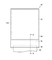
図4および図5は、本発明の1つの実施形態における有機EL表示装置の製造方法について説明するための図である。図4は製造工程において図2に示す表示パネルが切断される前の状態(表示パネル中間体と称する)を示す平面図であり、図5は図4のI−I断面の一例を示す図である。具体的には、図4に示す破線に沿って表示パネル中間体40aはカット(切断)され、図2に示す表示パネル40が得られる。1つの実施形態においては、カット(切断)は、個々のパネル(個片)に分割する際に行われる。なお、図5において、図3に示す表示パネル40の積層構造のうち、基材70から配線116までの積層構造を基板114として簡略化して示している。
4 and 5 are views for explaining a method of manufacturing an organic EL display device according to one embodiment of the present invention. 4 is a plan view showing a state before the display panel shown in FIG. 2 is cut (referred to as a display panel intermediate) in the manufacturing process, and FIG. 5 is a view showing an example of a cross section taken along line II in FIG. is there. Specifically, the display panel intermediate 40a is cut (cut) along the broken line shown in FIG. 4 to obtain the
表示パネル中間体40aには、部品実装領域46(曲げ領域120)の対向する両端部に、それぞれ、堰止部140が設けられており、樹脂層78の外縁は、堰止部140の側面まで達している。具体的には、堰止部140の側面に樹脂層78の外縁が接している。堰止部140は、カットラインLの外側にカットラインに沿う方向に延びるライン状に形成されており、樹脂層78は、表面フィルム132と堰止部140に囲まれた領域を埋めている。
The display panel
図5に示すように、堰止部140は、所定の間隔をあけて形成された一対の第1堰止部(突条部)141,141と、一対の第1堰止部141,141の外側に所定の間隔をあけて形成された一対の第2堰止部(突条部)142,142と、一対の第1堰止部141,141に挟まれた領域を埋める第3堰止部(バンク)143と、一対の第2堰止部142,142に挟まれた領域を埋めて第1堰止部141および第3堰止部143を覆う第4堰止部(バンク)144から構成される。
As shown in FIG. 5, the damming
第1堰止部141および第2堰止部142は、例えば、表示領域42において、基材70上に画素(回路層74およびOLED6)を形成する際に形成される。第1堰止部141および第2堰止部142を形成する材料は、特に限定されず、無機材料であってもよいし、有機材料(樹脂材料)であってもよいし、これらの混合物であってもよい。第1堰止部141および第2堰止部142の高さは、例えば2μmである。このような高さを満足させやすいことから、第1堰止部141および第2堰止部142は、樹脂材料で形成されるのが好ましい。具体的には、第1堰止部141および第2堰止部142は、それぞれ、表示領域42において、平坦化膜96および/またはリブ112を形成する際に形成される。
The
第3堰止部143は樹脂材料を含み、例えば、表示領域42において、基材70上に封止平坦化膜160を形成する際に形成される。具体的には、予め設けられた一対の第1堰止部141,141に挟まれた領域に樹脂組成物を塗布して、前記領域を樹脂組成物で埋める。第3堰止部143の高さは、例えば10μmである。
The
第4堰止部144は樹脂材料を含み、例えば、表示領域42において、基材70上に保護層108を形成する際に形成される。具体的には、予め設けられた一対の第2堰止部142,142に挟まれた領域に樹脂組成物を塗工して、前記領域を樹脂組成物で埋め、第1堰止部141および第3堰止部143を覆う。第4堰止部144の高さは、例えば20μmである。
The
基材70上に堰止部140を形成した後に、樹脂層78が形成される。具体的には、表面フィルム132と堰止部140に囲まれた領域を埋め、曲げ領域120および予め実装されたFPC50の端部を覆うように、インクジェット方式等により樹脂組成物を塗布して樹脂層78を形成する。堰止部140を設けることにより、一定の品質を有する製品を歩留りよく製造し得る。具体的には、均一に塗布する観点から樹脂組成物の粘度を低くした場合、樹脂組成物が外方に流れて所望の形成領域を越えて樹脂層78が形成されるおそれがある。逆に、塗布精度を上げるために樹脂組成物の粘度を低くした場合、所望の領域に樹脂組成物を均一に塗布することができないおそれがある。堰止部140を設けることにより、このような不具合を防止し得る。また、堰止部140を設けることにより、形成される樹脂層78の厚みを良好に制御でき、例えば、表示パネルを曲げた際の中立面を良好に制御し得る。
After forming the blocking
堰止部140の配置・形状(厚み)等は、例えば、樹脂層78の形成領域・厚み等に応じて決定される。具体的には、堰止部140の側面で塗布された樹脂組成物が堰き止められるので、所望の樹脂層78の形成領域および厚みに応じて、堰止部140の配置・形状(厚み)が決定される。図示例では、破線で示す所望の樹脂組成物の塗布端に合わせて、堰止部140の上面端部が位置している。塗布された樹脂組成物に、必要に応じて、任意の適切な処理(例えば、光照射、加熱、乾燥等)を施した後、カットラインLに沿って表示パネル中間体40aの対向する両端部を切断して表示パネル40が得られる。なお、本実施形態では、FPC50実装部分は、曲げ領域120ほど樹脂層78の厚みの均一性は求められないので、FPC50が実装される辺には、堰止部を設けていない。
The arrangement / shape (thickness) and the like of the damming
図6は、図4のI−I断面の変形例を示す図である。本変形例では、第2堰止部142,142および第4堰止部144を設けない点が、上記実施形態と異なっている。上記実施形態に比べて、堰止部140の高さは低くなるものの、堰止部140の形成領域を狭くできる。ここで、第3堰止部143は、例えば、表示領域42において、封止平坦化膜160および/または保護層108を形成する際に形成される。
FIG. 6 is a view showing a modification of the II cross section of FIG. The present modification is different from the above embodiment in that the
図7は、図1に示す有機EL表示装置の表示パネルの変形例を示す模式的な平面図である。本変形例では、上記実施形態の表示パネル中間体40aの部品実装領域46の両端部に形成された堰止部140,140が製品(表示パネル40)に残っている点が、上記実施形態と異なる。本変形例では、例えば、表示パネル40を曲げた際に堰止部140が破損することを防止する観点から、堰部140は有機材料(樹脂材料)で形成されるのが好ましい。
FIG. 7 is a schematic plan view showing a modification of the display panel of the organic EL display device shown in FIG. In this modification, the
本発明は、上記実施形態に限定されるものではなく、種々の変形が可能である。例えば、上記実施形態で示した構成と実質的に同一の構成、同一の作用効果を奏する構成または同一の目的を達成することができる構成で置き換えることができる。 The present invention is not limited to the above embodiment, and various modifications can be made. For example, it can be replaced with a configuration that is substantially the same as the configuration shown in the above embodiment, a configuration that exhibits the same operational effects, or a configuration that can achieve the same purpose.
本発明の思想の範疇において、当業者であれば、各種の変更例および修正例に想到し得るものであり、それら変更例および修正例についても本発明の範囲に属するものと了解される。例えば、前述の各実施形態に対して、当業者が適宜、構成要素の追加、削除もしくは設計変更を行ったもの、または、工程の追加、省略もしくは条件変更を行ったものも、本発明の要旨を備えている限り、本発明の範囲に含まれる。 In the scope of the idea of the present invention, those skilled in the art can conceive various changes and modifications, and it is understood that these changes and modifications also belong to the scope of the present invention. For example, those in which the person skilled in the art has appropriately added, deleted, or changed the design of the above-described embodiments, or those in which processes have been added, omitted, or changed conditions are also included in the gist of the present invention. As long as it is provided, it is included in the scope of the present invention.
2 有機EL表示装置、4 画素アレイ部、6 OLED、8 画素回路、10 点灯TFT、12 駆動TFT、14 キャパシタ、20 走査線駆動回路、22 映像線駆動回路、24 駆動電源回路、26 制御装置、28 走査信号線、30 映像信号線、32 駆動電源線、40 表示パネル、42 表示領域、44 額縁領域、46 部品実装領域、50 FPC、70 基材、72 TFT、74 回路層、78 樹脂層、80 下地層、82 半導体領域、84 ゲート絶縁膜、86 ゲート電極、88 層間絶縁層、90a ソース電極、90b ドレイン電極、92 層間絶縁膜、94 配線、96 平坦化膜、98 パッシベーション膜、100 下部電極、102 有機材料層、104 上部電極、106 封止層、108 保護層、110 コンタクトホール、112 リブ、116 配線、120 曲げ領域、130 接着層、132 表面フィルム、140 堰止部、160 封止平坦化膜、161 第1封止膜、162 第2封止膜。 2 organic EL display device, 4 pixel array unit, 6 OLED, 8 pixel circuit, 10 lighting TFT, 12 driving TFT, 14 capacitor, 20 scanning line driving circuit, 22 video line driving circuit, 24 driving power supply circuit, 26 control device, 28 scanning signal lines, 30 video signal lines, 32 drive power lines, 40 display panel, 42 display area, 44 frame area, 46 component mounting area, 50 FPC, 70 base material, 72 TFT, 74 circuit layer, 78 resin layer, 80 underlayer, 82 semiconductor region, 84 gate insulating film, 86 gate electrode, 88 interlayer insulating layer, 90a source electrode, 90b drain electrode, 92 interlayer insulating film, 94 wiring, 96 planarization film, 98 passivation film, 100 lower electrode , 102 Organic material layer, 104 Upper electrode, 106 Sealing layer, 108 Protective layer, 110 Contact hole, 112 rib, 116 wiring, 120 bend region, 130 an adhesive layer, 132 a surface film, 140 damming portion 160 sealing the planarizing film, 161 a first sealing film, 162 a second sealing film.
Claims (14)
前記部品が実装された状態の前記基材の部品実装領域に、樹脂組成物を塗布すること、をこの順で含み、
前記塗布された樹脂組成物の外縁は、前記堰止部の側面まで達する、
表示装置の製造方法。 Forming a damming portion in the component mounting region of the flexible substrate having a display region including a plurality of pixels and a component mounting region on which a component is mounted; and
Applying a resin composition in this order to the component mounting region of the base material in a state where the component is mounted,
The outer edge of the applied resin composition reaches the side surface of the damming portion,
Manufacturing method of display device.
前記曲げ領域を覆うように、前記樹脂組成物を塗布する、請求項1または2に記載の製造方法。 The component mounting area includes a bending area located on the side where the display area is located,
The manufacturing method of Claim 1 or 2 which apply | coats the said resin composition so that the said bending area | region may be covered.
第1方向に沿い所定の間隔をあけて形成された一対の突条部と、
前記一対の突条部に挟まれた領域を埋めるバンクと、
を有する、請求項1から4のいずれかに記載の製造方法。 The damming portion is
A pair of ridges formed at predetermined intervals along the first direction;
A bank that fills a region sandwiched between the pair of protrusions;
The manufacturing method in any one of Claim 1 to 4 which has these.
前記封止層を構成する樹脂材料層を形成する際に前記バンクを形成する、請求項7に記載の製造方法。 Forming a sealing layer covering the display area;
The manufacturing method according to claim 7, wherein the bank is formed when the resin material layer constituting the sealing layer is formed.
前記無機材料膜の所定の領域をエッチングにより除去するためのマスクを形成する際に、前記バンクを形成する、請求項7または8に記載の製造方法。 Forming an inorganic material film covering the display area;
The manufacturing method according to claim 7 or 8, wherein the bank is formed when a mask for removing a predetermined region of the inorganic material film by etching is formed.
前記基材の部品実装領域の少なくとも一部を覆う樹脂層と、
前記基材の部品実装領域に設けられた堰止部と、を有し、
前記堰止部の側面に前記樹脂層の外縁が接している、
表示装置。 A flexible substrate having a display area including a plurality of pixels and a component mounting area on which a component is mounted;
A resin layer covering at least a part of the component mounting region of the substrate;
A damming portion provided in a component mounting region of the base material,
The outer edge of the resin layer is in contact with the side surface of the damming portion,
Display device.
前記樹脂層は、前記曲げ領域を覆う、請求項10に記載の表示装置。 The component mounting area includes a bending area located on the side where the display area is located,
The display device according to claim 10, wherein the resin layer covers the bending region.
第1方向に沿い所定の間隔をあけて形成された一対の突条部と、
前記一対の突条部に挟まれた領域を埋めるバンクと、
を有する、請求項10から13のいずれかに記載の表示装置。 The damming portion is
A pair of ridges formed at predetermined intervals along the first direction;
A bank that fills a region sandwiched between the pair of protrusions;
The display device according to claim 10, comprising:
Priority Applications (2)
| Application Number | Priority Date | Filing Date | Title |
|---|---|---|---|
| JP2018061797A JP2019174609A (en) | 2018-03-28 | 2018-03-28 | Display and method for manufacturing display |
| US16/364,939 US11094759B2 (en) | 2018-03-28 | 2019-03-26 | Display device and method of manufacturing display device |
Applications Claiming Priority (1)
| Application Number | Priority Date | Filing Date | Title |
|---|---|---|---|
| JP2018061797A JP2019174609A (en) | 2018-03-28 | 2018-03-28 | Display and method for manufacturing display |
Publications (1)
| Publication Number | Publication Date |
|---|---|
| JP2019174609A true JP2019174609A (en) | 2019-10-10 |
Family
ID=68055573
Family Applications (1)
| Application Number | Title | Priority Date | Filing Date |
|---|---|---|---|
| JP2018061797A Pending JP2019174609A (en) | 2018-03-28 | 2018-03-28 | Display and method for manufacturing display |
Country Status (2)
| Country | Link |
|---|---|
| US (1) | US11094759B2 (en) |
| JP (1) | JP2019174609A (en) |
Cited By (1)
| Publication number | Priority date | Publication date | Assignee | Title |
|---|---|---|---|---|
| WO2021060532A1 (en) | 2019-09-25 | 2021-04-01 | 三ツ星ベルト株式会社 | Rubber composition and friction transmission belt |
Family Cites Families (16)
| Publication number | Priority date | Publication date | Assignee | Title |
|---|---|---|---|---|
| KR102173801B1 (en) * | 2012-07-12 | 2020-11-04 | 가부시키가이샤 한도오따이 에네루기 켄큐쇼 | Display device and method for manufacturing display device |
| JP6135062B2 (en) * | 2012-08-07 | 2017-05-31 | セイコーエプソン株式会社 | LIGHT EMITTING DEVICE, LIGHT EMITTING DEVICE MANUFACTURING METHOD, ELECTRONIC DEVICE |
| JP6561399B2 (en) * | 2013-11-20 | 2019-08-21 | 株式会社Joled | Display device and manufacturing method thereof |
| JP6219696B2 (en) * | 2013-11-27 | 2017-10-25 | 株式会社ジャパンディスプレイ | Light emitting display device and method for manufacturing light emitting display device |
| KR20150061921A (en) * | 2013-11-28 | 2015-06-05 | 엘지디스플레이 주식회사 | Organic Light Emitting Diode Display Device |
| US9513514B2 (en) * | 2014-03-14 | 2016-12-06 | Innolux Corporation | Display device |
| JP6397654B2 (en) * | 2014-05-13 | 2018-09-26 | 株式会社ジャパンディスプレイ | Organic EL light emitting device |
| KR20150145525A (en) * | 2014-06-20 | 2015-12-30 | 엘지디스플레이 주식회사 | Organic light emitting display device |
| JP6253541B2 (en) | 2014-07-30 | 2017-12-27 | 株式会社ジャパンディスプレイ | Display device |
| KR102182828B1 (en) * | 2014-08-14 | 2020-11-26 | 엘지디스플레이 주식회사 | Organic light emitting display panel |
| KR102263982B1 (en) * | 2014-10-20 | 2021-06-11 | 엘지디스플레이 주식회사 | Display apparatus |
| JP2016188976A (en) * | 2015-03-30 | 2016-11-04 | 株式会社ジャパンディスプレイ | Display device |
| US9716248B2 (en) * | 2015-12-18 | 2017-07-25 | Apple Inc. | Organic light-emitting diode displays with reduced border area |
| JP2017147165A (en) | 2016-02-19 | 2017-08-24 | 株式会社ジャパンディスプレイ | Display device |
| KR101898217B1 (en) * | 2016-12-29 | 2018-09-12 | 엘지디스플레이 주식회사 | Testing apparatus and testing method using the same |
| JP2018205486A (en) * | 2017-06-02 | 2018-12-27 | 株式会社ジャパンディスプレイ | Display and method for manufacturing display |
-
2018
- 2018-03-28 JP JP2018061797A patent/JP2019174609A/en active Pending
-
2019
- 2019-03-26 US US16/364,939 patent/US11094759B2/en active Active
Cited By (1)
| Publication number | Priority date | Publication date | Assignee | Title |
|---|---|---|---|---|
| WO2021060532A1 (en) | 2019-09-25 | 2021-04-01 | 三ツ星ベルト株式会社 | Rubber composition and friction transmission belt |
Also Published As
| Publication number | Publication date |
|---|---|
| US11094759B2 (en) | 2021-08-17 |
| US20190305061A1 (en) | 2019-10-03 |
Similar Documents
| Publication | Publication Date | Title |
|---|---|---|
| US9922909B2 (en) | Display device | |
| JP6253541B2 (en) | Display device | |
| JP6169005B2 (en) | Light emitting element display device | |
| JP6211873B2 (en) | Organic EL display device and method of manufacturing organic EL display device | |
| JP6872343B2 (en) | Display device and manufacturing method of display device | |
| JP6397654B2 (en) | Organic EL light emitting device | |
| JP6324098B2 (en) | Display device and manufacturing method thereof | |
| JP2018194632A (en) | Display device and method for manufacturing display device | |
| US11349098B2 (en) | Display device with an improved sealing layer | |
| JP2020109452A (en) | Display device and manufacturing method for display device | |
| JP2017146463A (en) | Display device | |
| JP2019179696A (en) | Organic el display and method for manufacturing organic el display | |
| JP6223070B2 (en) | Organic EL display device and method of manufacturing organic EL display device | |
| JP7178216B2 (en) | DISPLAY DEVICE AND METHOD FOR MANUFACTURING DISPLAY DEVICE | |
| JP2019003040A (en) | Display | |
| JP2019020509A (en) | Display and method for manufacturing display | |
| JP2019174609A (en) | Display and method for manufacturing display | |
| US10777633B2 (en) | Display device, display device manufacturing method, and display device manufacturing apparatus | |
| WO2019171878A1 (en) | Organic el display device | |
| JP2020027883A (en) | Organic el display and method for manufacturing organic el display | |
| JP7002629B2 (en) | Element substrate | |
| WO2019188116A1 (en) | Organic el display device and method for producing organic el display device | |
| JP2018205583A (en) | Display | |
| WO2018173415A1 (en) | Display device | |
| WO2021053955A1 (en) | Display device and method of manufacturing display device |