JP6134975B2 - Measuring device, measuring apparatus and method - Google Patents
Measuring device, measuring apparatus and method Download PDFInfo
- Publication number
- JP6134975B2 JP6134975B2 JP2013080164A JP2013080164A JP6134975B2 JP 6134975 B2 JP6134975 B2 JP 6134975B2 JP 2013080164 A JP2013080164 A JP 2013080164A JP 2013080164 A JP2013080164 A JP 2013080164A JP 6134975 B2 JP6134975 B2 JP 6134975B2
- Authority
- JP
- Japan
- Prior art keywords
- light
- convex structure
- measurement
- fine concavo
- sample
- Prior art date
- Legal status (The legal status is an assumption and is not a legal conclusion. Google has not performed a legal analysis and makes no representation as to the accuracy of the status listed.)
- Active
Links
Images


Classifications
-
- H—ELECTRICITY
- H01—ELECTRIC ELEMENTS
- H01J—ELECTRIC DISCHARGE TUBES OR DISCHARGE LAMPS
- H01J49/00—Particle spectrometers or separator tubes
- H01J49/02—Details
- H01J49/10—Ion sources; Ion guns
- H01J49/16—Ion sources; Ion guns using surface ionisation, e.g. field-, thermionic- or photo-emission
- H01J49/161—Ion sources; Ion guns using surface ionisation, e.g. field-, thermionic- or photo-emission using photoionisation, e.g. by laser
- H01J49/164—Laser desorption/ionisation, e.g. matrix-assisted laser desorption/ionisation [MALDI]
-
- G—PHYSICS
- G01—MEASURING; TESTING
- G01N—INVESTIGATING OR ANALYSING MATERIALS BY DETERMINING THEIR CHEMICAL OR PHYSICAL PROPERTIES
- G01N21/00—Investigating or analysing materials by the use of optical means, i.e. using sub-millimetre waves, infrared, visible or ultraviolet light
- G01N21/62—Systems in which the material investigated is excited whereby it emits light or causes a change in wavelength of the incident light
- G01N21/63—Systems in which the material investigated is excited whereby it emits light or causes a change in wavelength of the incident light optically excited
- G01N21/65—Raman scattering
- G01N21/658—Raman scattering enhancement Raman, e.g. surface plasmons
-
- H—ELECTRICITY
- H01—ELECTRIC ELEMENTS
- H01J—ELECTRIC DISCHARGE TUBES OR DISCHARGE LAMPS
- H01J49/00—Particle spectrometers or separator tubes
- H01J49/0004—Imaging particle spectrometry
-
- H—ELECTRICITY
- H01—ELECTRIC ELEMENTS
- H01J—ELECTRIC DISCHARGE TUBES OR DISCHARGE LAMPS
- H01J49/00—Particle spectrometers or separator tubes
- H01J49/02—Details
- H01J49/04—Arrangements for introducing or extracting samples to be analysed, e.g. vacuum locks; Arrangements for external adjustment of electron- or ion-optical components
- H01J49/0409—Sample holders or containers
- H01J49/0418—Sample holders or containers for laser desorption, e.g. matrix-assisted laser desorption/ionisation [MALDI] plates or surface enhanced laser desorption/ionisation [SELDI] plates
-
- G—PHYSICS
- G01—MEASURING; TESTING
- G01N—INVESTIGATING OR ANALYSING MATERIALS BY DETERMINING THEIR CHEMICAL OR PHYSICAL PROPERTIES
- G01N2201/00—Features of devices classified in G01N21/00
- G01N2201/06—Illumination; Optics
- G01N2201/061—Sources
- G01N2201/06113—Coherent sources; lasers
-
- G—PHYSICS
- G01—MEASURING; TESTING
- G01N—INVESTIGATING OR ANALYSING MATERIALS BY DETERMINING THEIR CHEMICAL OR PHYSICAL PROPERTIES
- G01N2201/00—Features of devices classified in G01N21/00
- G01N2201/06—Illumination; Optics
- G01N2201/068—Optics, miscellaneous
-
- H—ELECTRICITY
- H01—ELECTRIC ELEMENTS
- H01J—ELECTRIC DISCHARGE TUBES OR DISCHARGE LAMPS
- H01J49/00—Particle spectrometers or separator tubes
- H01J49/26—Mass spectrometers or separator tubes
- H01J49/34—Dynamic spectrometers
- H01J49/40—Time-of-flight spectrometers
Landscapes
- Physics & Mathematics (AREA)
- Chemical & Material Sciences (AREA)
- Analytical Chemistry (AREA)
- Optics & Photonics (AREA)
- Health & Medical Sciences (AREA)
- Pathology (AREA)
- Biochemistry (AREA)
- General Health & Medical Sciences (AREA)
- General Physics & Mathematics (AREA)
- Immunology (AREA)
- Life Sciences & Earth Sciences (AREA)
- Nuclear Medicine, Radiotherapy & Molecular Imaging (AREA)
- Engineering & Computer Science (AREA)
- Plasma & Fusion (AREA)
- Spectroscopy & Molecular Physics (AREA)
- Investigating, Analyzing Materials By Fluorescence Or Luminescence (AREA)
- Other Investigation Or Analysis Of Materials By Electrical Means (AREA)
Description
本発明は、光測定および質量分析との両方に用いられる測定用デバイス、その測定用デバイスを用いて光測定および質量分析との両方を行う測定装置および方法に関するものである。 The present invention relates to a measuring device used for both optical measurement and mass spectrometry, and a measuring apparatus and method for performing both optical measurement and mass spectrometry using the measuring device.
従来、物質の同定等に用いられる分析法において、基板の表面に付着した被分析物質を基板表面から脱離させ、イオン化させてその物質の質量と荷電の比によって物質を同定する、質量分析方法が知られている(特許文献1から特許文献3参照)。たとえば、飛行時間型質量分析法(Time of Flight Mass Spectroscopy : TOF-MS)は、イオン化した被分析物質を高電圧電極間で所定距離飛行させて、その飛行時間により物質の質量を分析するものである。
Conventionally, in an analysis method used for identification of a substance, the substance to be analyzed attached to the surface of the substrate is desorbed from the substrate surface, ionized, and the substance is identified by the ratio of the mass to the charge of the substance. Is known (see
このような質量分析法における被分析物質の脱離、イオン化の一つとして、レーザ照射を用いたレーザ脱離イオン化法があり、このようなレーザ脱離イオン化法の一つとして、SELDI法(Surface-Enhanced Laser Desorption / Ionization)が提案されている。 As one of the desorption and ionization of the analyte in such mass spectrometry, there is a laser desorption ionization method using laser irradiation. As one of such laser desorption ionization methods, a SELDI method (Surface -Enhanced Laser Desorption / Ionization) has been proposed.
SELDI法は、チップ表面に固定した化学官能基や分子を利用して、試料中に存在している特定の性質を持つ被分析物質をチップ上に捕捉、精製し、その後レーザ照射をすることで捕捉された被分析物質の脱離、イオン化を行う手法である。 The SELDI method uses chemical functional groups and molecules immobilized on the chip surface to capture and purify analytes with specific properties existing in the sample on the chip, and then irradiate with laser. This is a technique for desorbing and ionizing the captured analyte.
一方、上述したような物質の質量分析と同様に、物質の同定を行う方法として、ラマン分光法が知られている。ラマン分光法は、物質に単波長光を照射して得られる散乱光を分光して、ラマン散乱光のスペクトル(ラマンスペクトル)を得る方法であり、このスペクトルを解析することによって物質の同定などを行うことができる。 On the other hand, Raman spectroscopy is known as a method for identifying a substance, as in the mass spectrometry of a substance as described above. Raman spectroscopy is a method of obtaining a spectrum of Raman scattered light (Raman spectrum) by dispersing scattered light obtained by irradiating a substance with a single wavelength light. Analyzing this spectrum enables identification of the substance. It can be carried out.
上述したラマン分光法として、微弱なラマン散乱光を増強するために局在プラズモン共鳴によって増強された光電場を利用した、いわゆる表面増強ラマン(SERS)と呼ばれる方法がある。 As the Raman spectroscopy described above, there is a so-called surface enhanced Raman (SERS) method using a photoelectric field enhanced by localized plasmon resonance in order to enhance weak Raman scattered light.
この方法は、金属体、特に表面にナノオーダの凹凸を有する金属体に物質を接触させた状態で光を照射すると、局在プラズモン共鳴による光電場増強が生じ、金属体表面に接触された試料のラマン散乱光強度が増強されるという原理を利用するものである。 In this method, when light is irradiated in a state where a substance is in contact with a metal body, particularly a metal body having nano-order irregularities on the surface, a photoelectric field enhancement due to localized plasmon resonance occurs, and the sample in contact with the surface of the metal body This utilizes the principle that the Raman scattered light intensity is enhanced.
ここで、上述した質量分析法は、試料に対してレーザ照射を行うことによって被分析物質を基板表面から脱離させ、イオン化させる方法であるため、たとえば試料が生体の細胞などである場合には、その細胞内部および表面を含めたトータルな物質量の情報が得られることになる。 Here, since the mass spectrometry described above is a method in which the analyte is desorbed from the surface of the substrate by irradiating the sample with a laser and ionized, for example, when the sample is a living cell or the like. Thus, information on the total amount of substance including the inside and the surface of the cell can be obtained.
一方で、上述したSERS法は、金属体表面に接触された試料のラマン散乱光強度を検出するものであるため、試料の金属体表面との接触面近傍の情報が取得されることになり、たとえば細胞からしみ出して金属体の表面に付着した代謝物などの情報を取得することができ、質量分析法とは異なる情報が取得されることが期待される。 On the other hand, since the SERS method described above is for detecting the Raman scattered light intensity of the sample in contact with the metal body surface, information on the vicinity of the contact surface with the metal body surface of the sample is acquired. For example, it is possible to acquire information such as metabolites that ooze out from cells and adhere to the surface of a metal body, and it is expected that information different from mass spectrometry is acquired.
しかしながら、同一の試料について、たとえば上述したSELDI法とSERS法との両方の測定を行う場合、SELDI法は、試料を分子オーダの微量で基板上に固着する必要があるので、上述したような代謝物を放出するような分厚い細胞などを試料として計測することができない。 However, for example, when both the SELDI method and the SERS method described above are measured on the same sample, the SELDI method needs to fix the sample on the substrate with a minute amount of molecular order. Thick cells that release objects cannot be measured as samples.
また、SELDI法による測定を行った場合、その測定によって基板上の試料が全て離脱して消失してしまい、その後にSERS法による測定ができない場合がある。 In addition, when the measurement by the SELDI method is performed, the sample on the substrate may be detached and disappear due to the measurement, and then the measurement by the SERS method may not be performed.
なお、上述した特許文献1〜特許文献3には、質量分析とSERS法のような光測定との両方を行うことについては何も提案されていない。
In
本発明は、上記事情に鑑み、同一試料を用いて質量分析とSERS法のような光測定との両方を行うことができ、これにより試料のトータルな物質量の情報と試料の表面近傍の情報との両方を取得することができる測定用デバイスとその測定用デバイスを用いた測定装置および方法とを提供することを目的とする。 In view of the above circumstances, the present invention can perform both mass spectrometry and light measurement such as the SERS method using the same sample, and thereby information on the total amount of material in the sample and information on the vicinity of the surface of the sample. It is an object of the present invention to provide a measuring device that can acquire both of the above and a measuring apparatus and method using the measuring device.
本発明の測定用デバイスは、表面に透明な微細凹凸構造を有する誘電体からなる透明誘電体基板と、微細凹凸構造表面に金属膜を形成して構成された金属微細凹凸構造層とを備え、金属微細凹凸構造層がその金属微細凹凸構造層内において導通しているものであり、金属微細凹凸構造層に対して電圧を印加するための電圧印加電極が設けられていることを特徴とする。 The measuring device of the present invention comprises a transparent dielectric substrate made of a dielectric having a transparent fine uneven structure on the surface, and a metal fine uneven structure layer formed by forming a metal film on the surface of the fine uneven structure, The metal fine concavo-convex structure layer is electrically conductive in the metal fine concavo-convex structure layer, and a voltage application electrode for applying a voltage to the metal fine concavo-convex structure layer is provided.
また、上記本発明の測定用デバイスは、金属微細凹凸構造層の表面抵抗率を、107Ω/cm以下とできる。 In the measurement device of the present invention, the surface resistivity of the metal fine concavo-convex structure layer can be 10 7 Ω / cm or less.
また、微細凹凸構造を、ベーマイトから形成することができる。 Moreover, a fine concavo-convex structure can be formed from boehmite.
また、金属膜を、Au、Ag、Cu、Al、Ptおよびこれらを主成分とする合金からなる群より選択される少なくとも1種の金属から形成することができる。 Further, the metal film can be formed of at least one metal selected from the group consisting of Au, Ag, Cu, Al, Pt and alloys containing these as main components.
また、測定位置を示すための位置マーカを設けることができる。 In addition, a position marker for indicating the measurement position can be provided.
また、位置マーカを、電圧印加電極に設けることができる。 A position marker can be provided on the voltage application electrode.
また、位置マーカを、電圧印加電極に設けられた空隙とできる。 Further, the position marker can be a gap provided in the voltage application electrode.
本発明の測定装置は、上記本発明の測定用デバイスと、測定用デバイスの金属膜に対して透明誘電体基板側から第1の光を照射し、その照射により金属膜の表面に誘起された局在プラズモンの光電場増強効果によって、その表面に増強された光電場を発生させる第1の光照射部と、測定用デバイスへの第1の光の照射により発生し、透明誘電体基板側から射出された光を検出する光検出部と、金属微細凹凸構造層に電圧印加電極を介して電圧印加した状態において、金属微細凹凸構造層の表面に設置された試料およびその試料上に供給されたマトリクス剤に対して、第1の光の照射側とは反対側から第2の光を照射し、その照射により試料中の質量分析の被分析物質を表面から脱離させる第2の光照射部と、その脱離した被分析物質を検出してその被分析物質の質量を分析する分析部とを備えたことを特徴とする。 The measurement apparatus of the present invention irradiates the measurement device of the present invention and the metal film of the measurement device with the first light from the transparent dielectric substrate side, and is induced on the surface of the metal film by the irradiation. A first light irradiating unit that generates an enhanced photoelectric field on the surface due to the enhanced electric field of the localized plasmon, and generated by irradiation of the first light to the measuring device, from the transparent dielectric substrate side In a state in which a voltage is applied to the metal fine concavo-convex structure layer via the voltage application electrode, and a light detection unit that detects the emitted light, the sample placed on the surface of the metal fine concavo-convex structure layer and the sample supplied to the sample A second light irradiation unit that irradiates the matrix agent with the second light from the side opposite to the first light irradiation side, and desorbs the analyte of mass spectrometry in the sample from the surface by the irradiation. And detect the desorbed analyte. Characterized by comprising an analysis unit for analyzing the mass of the analyte.
また、上記本発明の測定装置においては、第1の光および第2の光によって測定用デバイス上を2次元状に走査させる走査機構を設けることができる。 In the measurement apparatus of the present invention, a scanning mechanism that scans the measurement device two-dimensionally with the first light and the second light can be provided.
また、測定用デバイスとして上記位置マーカが設けられた測定用デバイスを用いる場合には、測定用デバイスに設けられた位置マーカの検出結果に基づいて、光検出部の検出結果に基づいて生成された光スペクトル分布画像と、分析部の分析結果に基づいて生成された質量スペクトル分布画像との位置合わせを行う位置合わせ部を設けることができる。 Further, when the measurement device provided with the position marker is used as the measurement device, the measurement device is generated based on the detection result of the light detection unit based on the detection result of the position marker provided on the measurement device. An alignment unit that performs alignment between the optical spectrum distribution image and the mass spectrum distribution image generated based on the analysis result of the analysis unit can be provided.
また、測定用デバイスの電圧印加電極に電圧を印加する電圧印加部を設けることができる。 In addition, a voltage application unit that applies a voltage to the voltage application electrode of the measuring device can be provided.
本発明の測定方法は、上記本発明の測定用デバイスの金属膜に対して透明誘電体基板側から第1の光を照射し、その照射により金属膜の表面に誘起された局在プラズモンの光電場増強効果によって、その表面に増強された光電場を発生させて透明誘電体基板側から射出された光を検出し、金属微細凹凸構造層に電圧印加電極を介して電圧印加した状態において、金属微細凹凸構造層の表面に設置された試料およびその試料上に供給されたマトリクス剤に対して、第1の光の照射側とは反対側から第2の光を照射し、その照射により試料中の質量分析の被分析物質を表面から脱離させ、その脱離した被分析物質を検出してその被分析物質の質量を分析することを特徴とする。 In the measurement method of the present invention, the metal film of the measurement device of the present invention is irradiated with the first light from the transparent dielectric substrate side, and the photoelectric of localized plasmon induced on the surface of the metal film by the irradiation. In a state where a photoelectric field enhanced by the field enhancement effect is generated to detect light emitted from the transparent dielectric substrate side and a voltage is applied to the metal fine concavo-convex structure layer via the voltage application electrode, The sample placed on the surface of the fine concavo-convex structure layer and the matrix agent supplied on the sample are irradiated with the second light from the side opposite to the first light irradiation side, and the irradiation results in the sample. The substance to be analyzed by mass spectrometry is desorbed from the surface, the desorbed analyte is detected, and the mass of the analyte is analyzed.
本発明の測定用デバイス、測定装置および方法によれば、透明誘電体基板を備えた測定用デバイスの金属膜に対して透明誘電体基板側から第1の光を照射し、その照射により金属膜の表面に誘起された局在プラズモンの光電場増強効果によって、その表面に増強された光電場を発生させて透明誘電体基板側から射出された光を検出し、かつ、金属微細凹凸構造層に電圧印加電極を介して電圧印加した状態において、金属微細凹凸構造層の表面に設置された試料およびその試料上に供給されたマトリクス剤に対して、第1の光の照射側とは反対側から第2の光を照射し、その照射により試料中の質量分析の被分析物質を表面から脱離させ、その脱離した被分析物質を検出してその被分析物質の質量を分析することができる。 According to the measurement device, the measurement apparatus, and the method of the present invention, the metal film of the measurement device including the transparent dielectric substrate is irradiated with the first light from the transparent dielectric substrate side, and the metal film is irradiated by the irradiation. By detecting the light emitted from the transparent dielectric substrate side by generating an enhanced photoelectric field on the surface due to the enhancement of the photoelectric field of localized plasmons induced on the surface of the metal, and in the metal fine concavo-convex structure layer In a state where a voltage is applied via the voltage application electrode, the sample placed on the surface of the metal fine concavo-convex structure layer and the matrix agent supplied on the sample are viewed from the side opposite to the first light irradiation side. By irradiating the second light, the analyte of mass spectrometry in the sample can be desorbed from the surface by the irradiation, and the desorbed analyte can be detected to analyze the mass of the analyte. .
すなわち、本発明の測定用デバイス、測定装置および方法によれば、同一試料を用いて質量分析とSERS法のような光測定との両方を行うことができ、これにより試料のトータルな物質量の情報と試料の表面近傍の情報との両方を取得することができる。 That is, according to the measuring device, measuring apparatus, and method of the present invention, it is possible to perform both mass spectrometry and optical measurement such as the SERS method using the same sample. Both information and information near the surface of the sample can be acquired.
このような2つの情報を組み合わせることによって、たとえばマウスの脳のような組織を試料として用いてATP(アデノシン三リン酸)を測定した場合、その組織内部の物質量だけでなく、その物質の組織による保持されやすさに関する情報も得ることができる。 By combining these two pieces of information, for example, when ATP (adenosine triphosphate) is measured using a tissue such as a mouse brain as a sample, not only the amount of the substance inside the tissue but also the tissue of the substance It is also possible to obtain information on the ease of being held.
また、試料上にマトリクス剤を供給して質量分析を行う、いわゆるMALDI(Matrix Assisted Laser Desorption / Ionization)法を用いるようにしたので、比較的分厚いサンプルを測定することができる。また、これにより質量分析の後に、試料が焼失してしまうのを防止することができ、SERS法のような光測定も続けて行うことができる。 In addition, since a so-called MALDI (Matrix Assisted Laser Desorption / Ionization) method, in which a matrix agent is supplied onto a sample and mass spectrometry is performed, a relatively thick sample can be measured. In addition, it is possible to prevent the sample from being burned out after the mass analysis, and it is possible to continuously perform light measurement like the SERS method.
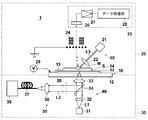
以下、本発明の測定用デバイス、測定装置および方法の一実施形態について、図面を参照しながら詳細に説明する。図1は、本実施形態の測定装置1の概略構成を示すブロック図である。
Hereinafter, an embodiment of a measuring device, a measuring apparatus, and a method of the present invention will be described in detail with reference to the drawings. FIG. 1 is a block diagram showing a schematic configuration of a
本実施形態の測定装置1は、測定用デバイス10の裏側(透明誘電体基板11側)から励起光を照射し、その励起光の照射により金属膜の表面に誘起された局在プラズモンの光電場増強効果によってその表面に増強された光電場を発生させ、測定用デバイス10の透明誘電体基板11から射出されたラマン散乱光を検出し、かつ、測定用デバイス10の金属微細凹凸構造層14の表面に設置された試料に対してその試料側から測定光を照射し、試料中の質量分析の被分析物質を表面から脱離させ、その脱離した被分析物質を検出して被分析物質の質量を分析するものである。すなわち、本実施形態の測定装置1は、測定用デバイス10に設置された試料のラマン散乱光の検出と、同じ試料中の被分析物質の質量分析との両方を行うことができるものである。
The
測定装置1は、図1に示すように、試料Sが設置される測定用デバイス10と、試料Sの質量分析を行う測定系20と、試料Sのラマン散乱光を測定する測定系30とを備えている。
As shown in FIG. 1, the
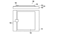
まず、本実施形態の測定用デバイス10について説明する。図2は、本実施形態の測定用デバイス10の側断面図(上図)と上面図(下図)を示すものである。
First, the
測定用デバイス10は、図2に示すように、表面に微細凹凸構造13を備えた透明誘電体基板11と、その微細凹凸構造13の表面に金属膜を形成して構成された金属微細凹凸構造層14と、金属微細凹凸構造層14に電圧印加するための電圧印加電極15とを備えたものである。
As shown in FIG. 2, the measuring
この測定用デバイス10は、金属微細凹凸構造層14の金属膜に励起光L1が照射されることによって、局在プラズモン共鳴が誘起され、この局在プラズモン共鳴により金属膜の表面に増強された光電場を発生するものである。
In this measuring
透明誘電体基板11は、ガラスなどの透明な誘電体からな基板本体12と、基板本体12とは異なる材料からなる微細凹凸構造13とから構成されている。なお、透明とは、励起光とラマン散乱光とに対して透過率が50%以上であることをいい、好ましくは75%以上、さらに好ましくは90%以上である。
The transparent
本実施形態における微細凹凸構造13は、ベーマイトから形成されるものである。微細凹凸構造13は、その表面の金属微細凹凸構造層14の凸部の深さの平均およびピッチの平均が、励起光L1の波長より短くなるように形成されるものであるが、金属微細凹凸構造層14の表面に局在プラズモンを生じさせうるものであればよい。特に、微細凹凸構造13は、凸部頂点から隣接する凹部の底部までの深さの平均が200nm以下、凹部を隔てた最隣接凸部の頂点同士のピッチの平均が200nm以下であることが望ましい。
The fine concavo-
金属微細凹凸構造層14は、励起光の照射を受けて局在プラズモンを生じうる金属からなるものであればよいが、たとえば、Au、Ag、Cu、Al、Ptおよびこれらを主成分とする合金からなる群より選択される少なくとも1種の金属からなるものである。特には、AuあるいはAgが好ましい。
The metal fine concavo-
金属微細凹凸構造層14の厚さは、微細凹凸構造13の表面に形成されたときに、金属微細凹凸構造として励起光の照射を受けて局在プラズモンを生じうる凹凸形状を維持することができる程度の厚みであれば特に制限はないが、10〜100nmであることが好ましい。
When formed on the surface of the fine concavo-
金属微細凹凸構造層14は、上述した質量分析の際には電圧印加されるものであり、導電性を有するものである。金属微細凹凸構造層14は、その表面抵抗率が107Ω/cm以下であることが望ましい。表面抵抗率は、金属微細凹凸構造層14と電圧印加電極15との任意の2点にプローブをあててテスターで測定された値である。
The metal fine concavo-
電圧印加電極15は、金属微細凹凸構造層14に接続され、金属微細凹凸構造層14に電圧印加するために用いられるものである。電圧印加電極15は、たとえばCr、Au、AlまたはAgなどから形成されるものである。
The
ここで、図3を用いて、本実施形態における測定用デバイス10の作製方法について説明する。図3は、測定用デバイス10の各作製工程における側断面図(上図)および上面図(下図)を示すものである。
Here, a manufacturing method of the
まず、板状の基板本体12を用意し、その基板本体12を純水洗浄する。その後、基板本体12の表面にマスクを用いてスパッタ法によりアルミニウム13aを数十nm程度成膜する。
First, a plate-
その後、純水を沸騰させた中に、アルミニウム13a付き基板本体12を浸水させ、数分(5分程度)後に取り出す。この煮沸処理(ベーマイト処理)により、アルミニウム13aは透明化し、微細凹凸構造13が形成される。
Thereafter, the
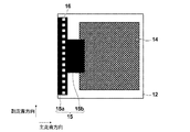
次に、微細凹凸構造13上に金属膜を蒸着させる。金属膜が微細凹凸構造13に沿って形成されることによって金属微細凹凸構造層14が構成される。図4は、微細凹凸構造13上に金属微細凹凸構造層14を形成した状態の一部拡大図を示すものである。なお、上述したように金属微細凹凸構造層14は導電性を有するように構成でされるが、一実施例として表面抵抗率が10−1Ω/cmのものが作製できた。
Next, a metal film is deposited on the fine concavo-
次いで、微細凹凸構造13および金属微細凹凸構造層14が形成されていない基板本体12の表面の一部の範囲と、金属微細凹凸構造層14の表面の端部とにマスクを用いてスパッタ法により電極材料が成膜され、これにより電圧印加電極15が形成される。
Next, a partial range of the surface of the
なお、上述した煮沸処理による微細凹凸構造作製工程において水熱反応させる金属としては、上述したアルミニウムに代えてアルミナ(Al(OH)3)のような金属酸化物を用いてもよい。アルミニウムおよびアルミナは、水熱反応させることにより、バイヤーマイト(Al[OH]3)またはベーマイト(AlOOH)のいずれか、または両方からなる複雑な三角錐構造を有する微細凹凸構造を基板上に形成することができる。なお、アルミニウムの他、チタン(Ti)など、同様に水熱反応により微細凹凸構造を形成する金属も用いることができる。 In addition, as the metal to be subjected to the hydrothermal reaction in the above-described micro uneven structure manufacturing process by the boiling process, a metal oxide such as alumina (Al (OH) 3 ) may be used instead of the above-described aluminum. Aluminum and alumina are subjected to a hydrothermal reaction to form a fine concavo-convex structure having a complicated triangular pyramid structure made of either buyerite (Al [OH] 3 ) or boehmite (AlOOH) or both on the substrate. be able to. In addition to aluminum, a metal that forms a fine relief structure by a hydrothermal reaction, such as titanium (Ti), can also be used.
また、金属あるいは金属酸化物を基板本体12に成膜する方法は、スパッタ法に限らず、加熱蒸着法やゾルゲル法を用いてもよい。
Further, the method of forming a metal or metal oxide film on the
また、水熱反応としては、煮沸処理に限らず、金属または金属酸化物が成膜された基板を高温の水蒸気に曝して金属または金属酸化物を高温の水蒸気と反応させる処理を行ってもよい。 In addition, the hydrothermal reaction is not limited to boiling treatment, and the substrate on which the metal or metal oxide film is formed may be exposed to high-temperature water vapor to cause the metal or metal oxide to react with high-temperature water vapor. .
また、微細凹凸構造13は、ベーマイト以外の透明な材料により構成されていてもよい。たとえばアルミニウム基体に対して、陽極酸化処理を施してその上層部に多数の微細孔を有する陽極酸化アルミナを作製し、陽極酸化されていないアルミニウム部分を除去した陽極酸化アルミナを微細凹凸構造13とし、これをガラスなどの基板本体12上に固定して透明誘電体基板11を構成するようにしてもよい。
The fine
また、微細凹凸構造は基板本体と異なる材料により構成されたもののみならず、基板本体の表面を加工することにより基板本体と同一の材料により構成されていてもよい。たとえばガラス基板の表面をリソグラフィーとドライエッチング処理することにより、表面に微細凹凸構造を形成したものを透明誘電体基板として用いてもよい。 Further, the fine concavo-convex structure is not limited to one made of a material different from that of the substrate body, but may be made of the same material as the substrate body by processing the surface of the substrate body. For example, a glass substrate having a surface with a fine concavo-convex structure formed by subjecting the surface to lithography and dry etching may be used as the transparent dielectric substrate.
次に、図1に戻り、本実施形態の測定装置1における質量分析測定系20について説明する。質量分析測定系20は、いわゆる飛行時間型質量分析装置(TOF−MS)である。
Next, returning to FIG. 1, the mass
質量分析測定系20は、測定用デバイス10の金属微細凹凸構造層14の表面に設置された試料Sおよびその試料S上に供給されたマトリクス剤Mに対して測定光L3(第2の光)を照射して、試料中の質量分析の被分析物質を測定用デバイス10の表面から脱離させる測定光照射部60(第2の光照射部)と、脱離した被分析物質を検出して被分析物質の質量を分析する分析部25とを備えている。
The mass
また、測定用デバイス10と分析部25との間には、測定用デバイス10の表面に対向する位置に配された引き出しグリッド23と、引き出しグリッド23の測定用デバイス10側の面と反対側の面に対向して配されたエンドプレート24とが設けられている。
In addition, between the
また、測定用デバイス10の電圧印加電極15に対して電圧を印加する電圧印加部29を備えている。
Further, a
測定光照射部60は、測定光L3を射出する半導体レーザ光源21と、半導体レーザ光源21から射出された測定光L3を試料に対して集光する集光光学系22とを備えている。測定光L3としては、たとえば波長337nm、パルス幅50ps〜50ns程度のパルスレーザ光を用いることができる。
The measurement
分析部25は、測定光L3の照射により測定用デバイス10の表面から脱離され、引き出しグリッド23およびエンドプレート24の中央の孔を通過して飛行してきた被分析物質を検出する検出器26と、検出器26の出力を増幅するアンプ27と、アンプ27からの出力信号を処理するデータ処理部28とを備えている。
The
次に、本実施形態の測定装置1におけるラマン散乱光測定系30について説明する。
Next, the Raman scattered
ラマン散乱光測定系30は、図1に示すように、測定用デバイス10の裏面側(透明誘電体基板11側)から励起光L1(第1の光)を照射する励起光照射部40(第1の光照射部)と、測定用デバイス10の金属微細凹凸構造層14近傍の物質から発せられ、光電場増強効果によって増強されたラマン散乱光L2を測定用デバイス10の裏面側から検出するための光検出部50とを備えている。
As shown in FIG. 1, the Raman scattered
励起光照射部40は、励起光L1を射出する半導体レーザ光源31と、この半導体レーザ光源31から射出された励起光L1を平行光化するレンズ32と、レンズ32によって平行光化された励起光L1を透過するとともに、かつその励起光L1の照射により測定用デバイス10の金属微細凹凸構造層14近傍の物質から射出されたラマン散乱光L2を含む光を光検出部50側へ反射するハーフミラー34と、ハーフミラー34を透過した励起光L1を金属微細凹凸構造層14近傍に集光するとともに、ラマン散乱光L2を平行光化するレンズ33とを備えている。
The excitation
光検出部50は、ハーフミラー34により反射されてきた光のうち励起光L1を除去し、それ以外の光を透過するノッチフィルタ35と、ノッチフィルタ35を透過したラマン散乱光L2を集光するためのレンズ36と、レンズ36によって集光されたラマン散乱光L2を分光器まで38まで導光する導光部37と、導光部37によって導光されたラマン散乱光L2を検出する分光器38とを備えている。
The
次に、本実施形態の測定装置1の質量分析測定系20を用いた質量分析と、ラマン散乱光測定系30を用いたラマン散乱光の検出について説明する。
Next, mass spectrometry using the mass
まず、図5に示すように、本実施形態の測定用デバイス10が用意され、その測定用デバイス10の金属微細凹凸構造層14の表面に、質量分析の被分析物質を含む試料Sが供給され、その試料Sの上にマトリクス剤Mが供給される。
First, as shown in FIG. 5, the
このマトリクス剤Mは、測定光L3を吸収して熱エネルギーに変換し、その熱エネルギーによって試料S中における被分析物質をマトリクス剤Mとともに気化させ、次いでマトリクス剤Mと被分析物質との間でのプロトン移動が起こって被分析物質をイオン化させるものである。まず、試料Sとして、被分析物質Aを含む試料とマトリクス剤Mとの混合試料を用意する。 The matrix agent M absorbs the measuring light L3 and converts it into thermal energy, and the analyte in the sample S is vaporized together with the matrix agent M by the thermal energy, and then between the matrix agent M and the analyte. The proton transfer occurs to ionize the analyte. First, as the sample S, a mixed sample of the sample containing the analyte A and the matrix agent M is prepared.
マトリクス剤Mとしては、従来のMALDI法で用いられている既知のマトリクス剤を用いることができる。具体的には、ニコチン酸、ピコリン酸、3-ヒドロキシピコリン酸、3-アミノピコリン酸、2,5-ジヒドロキシ安息香酸、α-シアノ-4-ヒドロキシ桂皮酸、シナピン酸、2-(4-ヒドロキシフェニルアゾ)安息香酸、2-メルカプトベンゾチアゾール、5-クロロ-2-メルカプトベンゾチアゾール、2,6-ジヒドロキシアセトフェノン、2,4,6-トリヒドロキシアセトフェノン、ジスラノール、ベンゾ[a]ピレン、9-ニトロアントラセン、2-[(2E)-3-(4-tret-ブチルフェニル)-2-メチルプロプ-2-エニリデン]マロノ二トリルなどをマトリクス剤Mとして用いることができる。 As the matrix agent M, a known matrix agent used in the conventional MALDI method can be used. Specifically, nicotinic acid, picolinic acid, 3-hydroxypicolinic acid, 3-aminopicolinic acid, 2,5-dihydroxybenzoic acid, α-cyano-4-hydroxycinnamic acid, sinapinic acid, 2- (4-hydroxy Phenylazo) benzoic acid, 2-mercaptobenzothiazole, 5-chloro-2-mercaptobenzothiazole, 2,6-dihydroxyacetophenone, 2,4,6-trihydroxyacetophenone, disranol, benzo [a] pyrene, 9-nitro Anthracene, 2-[(2E) -3- (4-tret-butylphenyl) -2-methylprop-2-enylidene] malononitryl and the like can be used as the matrix agent M.
そして、試料Sとマトリクス剤Mとが供給された測定用デバイス10の電圧印加電極15に対して、電圧印加部29によって所定の電圧が印加され、測定光照射部60から測定光L3が測定用デバイス10の表面に照射される。マトリクス剤Mによって測定光L3が吸収されて熱エネルギーに変換され、その熱エネルギーによって試料S中における被分析物質がマトリクス剤Mとともに気化され、測定用デバイス10の表面から離脱され、同時にイオン化される。
Then, a predetermined voltage is applied by the
脱離された被分析物質は、測定用デバイス10の電圧印加された金属微細凹凸構造層14と接地された引き出しグリッド23との電位差により引き出しグリッド23の方向に引き出されて加速し、中央の孔を通ってエンドプレート24の方向にほぼ直進して飛行し、さらにエンドプレート24の孔を通過して検出器26に到達して検出される。
The desorbed analyte is extracted in the direction of the extraction grid 23 due to a potential difference between the metal fine concavo-
脱離後の被分析物質の飛行速度は物質の質量に依存し、質量が小さいほど速いため、質量の小さいものから順に検出器26により検出される。 The flying speed of the analyte after desorption depends on the mass of the substance, and the smaller the mass, the faster the detection speed.
検出器26からの出力信号は、アンプ27により所定レベルに増幅され、その後データ処理部28に入力される。データ処理部28では、アンプ27からの出力信号に基づいて被分析物質の飛行時間が求められ、その飛行時間から質量を導出して質量スペクトルが得られる。
The output signal from the
次に、本実施形態の測定装置1のラマン散乱光測定系30を用いて、試料Sから放出された代謝物などのラマンスペクトルを測定する方法について説明する。なお、このラマンスペクトルの測定は、上述した質量分析と同時に行うようにしてもよいし、質量分析の前または後で行うようにしてもよい。
Next, a method for measuring a Raman spectrum of a metabolite released from the sample S using the Raman scattered
まず、上述したようにして試料Sとマトリクス剤Mが供給された測定用デバイス10に向けて、励起光照射部40の半導体レーザ光源31から励起光L1が射出され、励起光L1はレンズ32およびハーフミラー34を透過し、レンズ33で集光されて測定用デバイス10上の金属微細凹凸構造層14近傍に照射される。
First, as described above, the excitation light L1 is emitted from the semiconductor
励起光L1の照射によって金属微細凹凸構造層14において局在プラズモン共鳴が誘起され、金属微細凹凸構造層14の表面に増強された光電場が発生する。そして、金属微細凹凸構造層14近傍の物質から発せられ、光電場により増強されたラマン散乱光L2が、レンズ33を透過して、ハーフミラー34によって分光器38側に反射される。なお、このとき、測定用デバイス10で反射された励起光L1もハーフミラー34によって反射されて分光器38側に反射されるが、励起光L1はノッチフィルタ35によって除去される。
Irradiation with the excitation light L1 induces localized plasmon resonance in the fine metal concavo-
一方、励起光L1とは波長が異なる光はノッチフィルタ35を透過し、レンズ36によって導光部37に集光され、導光部37によって導光された光が分光器38へ入射され、分光器38によってラマンスペクトル測定が行われる。
On the other hand, light having a wavelength different from that of the excitation light L1 passes through the
上記実施形態の測定装置1によれば、同一試料を用いて質量分析とSERS法のような光測定との両方を行うことができ、これにより試料のトータルな物質量の情報と試料の表面近傍の情報との両方を取得することができる。
According to the
このような2つの情報を組み合わせることによって、たとえばマウスの脳のような組織を試料として用いてATP(アデノシン三リン酸)を測定した場合、その組織内部の物質量だけでなく、その物質の組織による保持されやすさに関する情報も得ることができる。 By combining these two pieces of information, for example, when ATP (adenosine triphosphate) is measured using a tissue such as a mouse brain as a sample, not only the amount of the substance inside the tissue but also the tissue of the substance It is also possible to obtain information on the ease of being held.
また、試料上にマトリクス剤を供給して質量分析を行う、いわゆるMALDI法を用いるようにしたので、比較的分厚いサンプルを測定することができる。また、これにより質量分析の後に、試料が焼失してしまうのを防止することができ、SERS法のような光測定も続けて行うことができる。 In addition, since a so-called MALDI method is used in which a matrix agent is supplied onto a sample and mass spectrometry is performed, a relatively thick sample can be measured. In addition, it is possible to prevent the sample from being burned out after the mass analysis, and it is possible to continuously perform light measurement like the SERS method.
また、上記実施形態の測定装置1において、励起光L1および測定光L3によって試料S上を2次元状に走査し、試料S上の励起光L1の各走査点についてラマンスペクトルを取得するとともに、測定光L3の各走査点について質量スペクトルを取得するようにしてもよい。
In the
具体的には、たとえば、図6に示すように、上記実施形態の測定装置1において、測定用デバイス10を保持するとともに、図6に示すX方向およびY方向(紙面厚さ方向)に測定用デバイス10を移動させる移動ステージ100を設け、この移動ステージ100によって測定用デバイス10を移動させることによって、測定用デバイス10を励起光L1および測定光L3によって2次元状に走査するようにしてもよい。
Specifically, for example, as shown in FIG. 6, in the
なお、励起光L1および測定光L3を2次元状に走査する走査機構としてはこれに限らず、測定用デバイス10は固定した状態とし、たとえばガルバノミラーなどを用いることによって測定用デバイス10を励起光L1および測定光L3によって2次元状に走査するようにしてもよい。
The scanning mechanism that scans the excitation light L1 and the measurement light L3 in a two-dimensional manner is not limited to this, and the
また、上記実施形態の測定装置1における質量分析測定系20とラマン散乱光測定系30とは、図1および図6に示すように一体化して構成するようにしてもよいし、これらの測定系を別々に構成するようにしてもよい。
Further, the mass
質量分析測定系20とラマン散乱光測定系30とを一体化して構成する場合には、質量分析測定系20の少なくともアンプ27とデータ処理部28とを除く構成と、ラマン散乱光測定系30の各構成とが、真空状態にされた真空ボックス内に配置される。
When the mass
また、上述した質量分析測定系20とラマン散乱光測定系30を別々に構成する場合には、質量分析測定系20の少なくともアンプ27とデータ処理部28とを除く構成が真空ボックス内に配置され、同一の測定用デバイス10を用いて質量分析とラマン散乱光の検出とがそれぞれ行われることになる。
In the case where the mass
ここで、上述したように測定系を別々に構成した場合や、測定系を一体化した構成において各測定系における測定を別々のタイミングで行う場合、上述したように測定用デバイス10を2次元状に走査して測定を行う際には、各測定系における測定位置を一致させる必要がある。
Here, when the measurement system is configured separately as described above, or when measurement in each measurement system is performed at different timings in a configuration in which the measurement system is integrated, the
そこで、測定用デバイス10に位置マーカを設け、その位置マーカの検出結果を用いて各測定系における測定位置を一致させるようにしてもよい。
Therefore, a position marker may be provided in the
図7は、測定用デバイス10の電圧印加電極15に位置マーカ16を形成した例を示すものである。図7に示す測定用デバイス10は、図7に示す主走査方向(X方向)に励起光L1および測定光L3が走査されるとともに、その主走査方向への走査が副走査方向(Y方向)に向けて順次繰り返して行われるものである。そして、位置マーカ16は、主走査方向に直交する副走査方向に所定の間隔を空けて点状に形成されたものである。位置マーカ16の各点の間隔は副走査方向への走査間隔と同じ間隔とすることが望ましい。
FIG. 7 shows an example in which the
ここで、図8を用いて、図7に示す測定用デバイス10の作製方法について説明する。なお、ここでは位置マーカ16の形成方法を中心に説明する。
Here, a manufacturing method of the
まず、板状の基板本体12の一辺の端部に対して、フォトリソグラフィおよびリフトオフによって位置マーカ16の部分が空隙となるマーカ付電極パターン15aを形成する。
First, an
次いで、マーカ付電極パターン15aが形成された後、上記実施形態と同様にして、ベーマイトからなる微細凹凸構造13が形成される。そして、その微細凹凸構造13上に金属膜を蒸着させることによって金属微細凹凸構造層14が構成される。
Next, after the marker-attached
次いで、マーカ付電極パターン15aと、金属微細凹凸構造層14の表面の端部との間に蒸着により接続電極パターン15bが形成され、マーカ付電極パターン15aと接続電極パターン15bとから電圧印加電極15が形成される。
Next, a
なお、位置マーカ16のパターンとしては、図7に示すパターン以外のパターンでもよい。また、位置マーカ16を形成する場所は、電圧印加電極15に限らす、たとえば、基板本体12の全体に、図9Aに示すようなストライプ状の金属パターンを形成するようにしてもよいし、図9Bに示すような格子状の金属パターンを形成するようにしてもよい。
Note that the pattern of the
図10は、上述したように測定用デバイス10に設けられた位置マーカ16を検出し、その検出結果に基づいて、各測定系における測定結果の位置合わせを行う測定装置1の構成を示すものである。
FIG. 10 shows the configuration of the
図10に示す測定装置1におけるラマン散乱光測定系30においては、測定用デバイス10の位置マーカ16が設けられた電圧印加電極15の範囲まで励起光L1によって走査され、位置マーカ16が設けられた電圧印加電極15からの反射光が分光器38によって検出され、その検出結果がラマン散乱光の検出結果と同様に位置合わせ部80に入力される。なお、電圧印加電極15からの反射光は、ノッチフィルタ35によって大部分がカットされるが完全にカットされる訳ではなく、一部が通過するのでこれを分光器38によって検出することができる。
In the Raman scattered
位置合わせ部80においては、各走査点において測定されたラマンスペクトルに基づいて、特定物質のラマンスペクトル分布画像が作成されるが、このとき位置マーカ16の画像が、ラマンスペクトル分布画像の座標空間上において予め設定された位置に配置されるようにして作成される。
In the
一方、図10に示す測定装置1における質量分析測定系20においては、測定光L3の測定用デバイス10上における反射光を検出する光検出器70が設けられている。
On the other hand, in the mass
そして、測定用デバイス10の位置マーカ16が設けられた電圧印加電極15の範囲まで測定光L3によって走査され、位置マーカ16が設けられた電圧印加電極15からの反射光が光検出器70によって検出され、その検出結果が位置合わせ部80に入力される。
Then, the measurement light L3 is scanned up to the range of the
位置合わせ部80においては、各走査点において測定された質量スペクトルに基づいて、特定物質の質量スペクトル分布画像が作成されるが、このとき位置マーカ16の画像が、質量スペクトル分布画像の座標空間上において予め設定された位置に配置されるようにして作成される。
In the
そして、上述した2つの分布画像の座標空間上の予め設定された位置をそれぞれの座標空間上で同じ位置にすることによって、これらの2つの分布画像の位置合わせを行うことができる。 The two distribution images can be aligned by setting the previously set positions on the coordinate spaces of the two distribution images to the same positions on the respective coordinate spaces.
位置合わせ部80によって生成された2つの分布画像は、所定の表示装置(図示省略)に出力され、表示装置において表示される。
The two distribution images generated by the
なお、上記説明では、電圧印加電極15に位置マーカ16として形成された空隙の反射パターンを検出するようにしたが、位置マーカ16としてはこのような空隙に限らず、電圧印加電極15よりも励起光L1や測定光L3に対して反射率が高い材料や、吸収率が高い材料を用いて位置マーカ16を形成するようにしてもよい。または、励起光L1および測定光L3の照射によって蛍光を発する材料を用いて位置マーカ16を形成するようにしてもよい。ただし、上述したように空隙から位置マーカ16を形成した場合には、電圧印加電極15の製造工程と同時に形成することができるので、新たな製造工程を設ける必要がなく、より好ましい。
In the above description, the reflection pattern of the gap formed as the
なお、上記実施形態の測定装置1においては、質量分析を行うとともに、ラマン散乱光を検出するようにしたが、ラマン散乱光に限らず、プラズモン増強蛍光検出法によって蛍光を検出するようにしてもよい。さらには、ラマン散乱光、蛍光の測定のみならず、励起光L1の照射を受けた金属膜近傍の物質から生じるレーリー散乱光、ミー散乱光、あるいは第2高調波などの測定装置および方法においても、上述の測定用デバイス10を用いることができる。
In the
1 測定装置
10 測定用デバイス
11 透明誘電体基板
12 基板本体
13 微細凹凸構造
14 金属微細凹凸構造層
15 電圧印加電極
15a マーカ付電極パターン
15b 接続電極パターン
16 位置マーカ
20 質量分析測定系
21 半導体レーザ光源
25 分析部
26 検出器
28 データ処理部
29 電圧印加部
30 ラマン散乱光測定系
31 半導体レーザ光源
34 ハーフミラー
38 分光器
40 励起光照射部
50 光検出部
60 測定光照射部
70 光検出器
80 位置合わせ部
100 移動ステージ
DESCRIPTION OF
Claims (12)
該微細凹凸構造表面に金属膜を形成して構成された金属微細凹凸構造層とを備え、
前記金属微細凹凸構造層が該金属微細凹凸構造層内において導通しているものであり、
前記金属微細凹凸構造層に対して該電圧を印加するための電圧印加電極が設けられていることを特徴とする測定用デバイス。 A transparent dielectric substrate made of a dielectric having a transparent fine relief structure on the surface;
A metal fine uneven structure layer formed by forming a metal film on the surface of the fine uneven structure,
The metal fine concavo-convex structure layer is electrically conductive in the metal fine concavo-convex structure layer,
A measuring device, wherein a voltage applying electrode for applying the voltage to the metal fine concavo-convex structure layer is provided.
該測定用デバイスの前記金属膜に対して前記透明誘電体基板側から第1の光を照射し、該照射により前記金属膜の表面に誘起された局在プラズモンの光電場増強効果によって、該表面に増強された光電場を発生させる第1の光照射部と、
前記測定用デバイスへの前記第1の光の照射により発生し、前記透明誘電体基板側から射出された光を検出する光検出部と、
前記金属微細凹凸構造層に前記電圧印加電極を介して電圧印加した状態において、前記金属微細凹凸構造層の表面に設置された試料および該試料上に供給されたマトリクス剤に対して、前記第1の光の照射側とは反対側から第2の光を照射し、該照射により前記試料中の質量分析の被分析物質を前記表面から脱離させる第2の光照射部と、
前記脱離した被分析物質を検出して該被分析物質の質量を分析する分析部とを備えたことを特徴とする測定装置。 A measuring device according to any one of claims 1 to 7 ,
By irradiating the metal film of the measuring device with the first light from the transparent dielectric substrate side, and by the effect of enhancing the photoelectric field of localized plasmons induced on the surface of the metal film by the irradiation, A first light irradiator for generating an enhanced photoelectric field;
A light detection unit that detects light emitted from the transparent dielectric substrate side generated by irradiation of the first light to the measurement device;
In a state in which a voltage is applied to the metal fine concavo-convex structure layer via the voltage application electrode, the first placed on the sample placed on the surface of the metal fine concavo-convex structure layer and the matrix agent supplied on the sample Irradiating the second light from the side opposite to the light irradiation side of the second light irradiation unit for desorbing the analyte of mass spectrometry in the sample from the surface by the irradiation,
A measuring apparatus comprising: an analysis unit that detects the desorbed analyte and analyzes the mass of the analyte.
前記測定用デバイスに設けられた位置マーカの検出結果に基づいて、前記光検出部の検出結果に基づいて生成された光スペクトル分布画像と、前記分析部の分析結果に基づいて生成された質量スペクトル分布画像との位置合わせを行う位置合わせ部を備えたことを特徴とする請求項8または9記載の測定装置。 A measuring device according to any one of claims 5 to 7 , comprising:
Based on the detection result of the position marker provided in the measurement device, the optical spectrum distribution image generated based on the detection result of the light detection unit, and the mass spectrum generated based on the analysis result of the analysis unit measuring apparatus according to claim 8 or 9, wherein further comprising a positioning unit for performing positioning between distribution image.
該照射により前記金属膜の表面に誘起された局在プラズモンの光電場増強効果によって、該表面に増強された光電場を発生させて前記透明誘電体基板側から射出された光を検出し、
前記金属微細凹凸構造層に前記電圧印加電極を介して電圧印加した状態において、前記金属微細凹凸構造層の表面に設置された試料および該試料上に供給されたマトリクス剤に対して、前記第1の光の照射側とは反対側から第2の光を照射し、
該照射により前記試料中の質量分析の被分析物質を前記表面から脱離させ、
該脱離した被分析物質を検出して該被分析物質の質量を分析することを特徴とする測定方法。 Irradiating the first light from the transparent dielectric substrate side with respect to the metal film of the measuring device of claims 1 to 7 any one of claims,
By detecting the light emitted from the transparent dielectric substrate side by generating an enhanced photoelectric field on the surface by the photoelectric field enhancement effect of localized plasmons induced on the surface of the metal film by the irradiation,
In a state in which a voltage is applied to the metal fine concavo-convex structure layer via the voltage application electrode, the first placed on the sample placed on the surface of the metal fine concavo-convex structure layer and the matrix agent supplied on the sample Irradiate the second light from the opposite side of the light irradiation side,
Desorbing the analyte of mass spectrometry in the sample from the surface by the irradiation,
A measurement method comprising detecting the desorbed analyte and analyzing the mass of the analyte.
Priority Applications (3)
| Application Number | Priority Date | Filing Date | Title |
|---|---|---|---|
| JP2013080164A JP6134975B2 (en) | 2013-04-08 | 2013-04-08 | Measuring device, measuring apparatus and method |
| PCT/JP2014/001985 WO2014167828A1 (en) | 2013-04-08 | 2014-04-07 | Measurement device, measurement apparatus, and method |
| US14/875,129 US9728388B2 (en) | 2013-04-08 | 2015-10-05 | Measurement device, measurement apparatus, and method |
Applications Claiming Priority (1)
| Application Number | Priority Date | Filing Date | Title |
|---|---|---|---|
| JP2013080164A JP6134975B2 (en) | 2013-04-08 | 2013-04-08 | Measuring device, measuring apparatus and method |
Publications (3)
| Publication Number | Publication Date |
|---|---|
| JP2014202650A JP2014202650A (en) | 2014-10-27 |
| JP2014202650A5 JP2014202650A5 (en) | 2016-01-21 |
| JP6134975B2 true JP6134975B2 (en) | 2017-05-31 |
Family
ID=51689250
Family Applications (1)
| Application Number | Title | Priority Date | Filing Date |
|---|---|---|---|
| JP2013080164A Active JP6134975B2 (en) | 2013-04-08 | 2013-04-08 | Measuring device, measuring apparatus and method |
Country Status (3)
| Country | Link |
|---|---|
| US (1) | US9728388B2 (en) |
| JP (1) | JP6134975B2 (en) |
| WO (1) | WO2014167828A1 (en) |
Families Citing this family (10)
| Publication number | Priority date | Publication date | Assignee | Title |
|---|---|---|---|---|
| WO2016142674A1 (en) | 2015-03-06 | 2016-09-15 | Micromass Uk Limited | Cell population analysis |
| GB2554180B (en) | 2015-03-06 | 2022-04-13 | Micromass Ltd | Spectrometric analysis |
| CN107667288B (en) | 2015-03-06 | 2022-02-01 | 英国质谱公司 | Spectral analysis of microorganisms |
| JP6717298B2 (en) * | 2015-05-08 | 2020-07-01 | Agc株式会社 | Sample plate for mass spectrometry, mass spectrometry method and mass spectrometer |
| GB201517195D0 (en) * | 2015-09-29 | 2015-11-11 | Micromass Ltd | Capacitively coupled reims technique and optically transparent counter electrode |
| JP6534215B2 (en) * | 2016-01-05 | 2019-06-26 | 日本電子株式会社 | Measuring method |
| EP3418732B1 (en) * | 2016-03-18 | 2024-01-31 | Citizen Finedevice Co., Ltd. | Sample mounting plate and method for manufacturing the same |
| US11454611B2 (en) | 2016-04-14 | 2022-09-27 | Micromass Uk Limited | Spectrometric analysis of plants |
| EP3336877B1 (en) * | 2016-12-13 | 2021-04-14 | University-Industry Foundation(UIF), Yonsei University | Sample plate, method of fabricating the same and mass spectrometer analysis by using the same |
| CN113092374B (en) * | 2021-04-12 | 2022-11-15 | 青岛科技大学 | Small vacuum photoelectric test system |
Family Cites Families (13)
| Publication number | Priority date | Publication date | Assignee | Title |
|---|---|---|---|---|
| GB9518429D0 (en) * | 1995-09-08 | 1995-11-08 | Pharmacia Biosensor | A rapid method for providing kinetic and structural data in molecular interaction analysis |
| JP2007171003A (en) | 2005-12-22 | 2007-07-05 | Fujifilm Corp | Substrate for mass spectrometry, analytical method, and apparatus |
| JP5049549B2 (en) | 2006-10-25 | 2012-10-17 | キヤノン株式会社 | Substrate for mass spectrometry, method for producing the same, and mass spectrometer |
| JP5069497B2 (en) | 2007-05-24 | 2012-11-07 | 富士フイルム株式会社 | Device for mass spectrometry and mass spectrometer using the same |
| JP4993360B2 (en) | 2007-06-08 | 2012-08-08 | 富士フイルム株式会社 | MICROSTRUCTURE, MANUFACTURING METHOD THEREOF, PHOTOELECTRIC FIELD ENHANCER DEVICE |
| US8071938B2 (en) * | 2008-03-20 | 2011-12-06 | The Mitre Corporation | Multi-modal particle detector |
| WO2010044274A1 (en) * | 2008-10-17 | 2010-04-22 | 国立大学法人東京工業大学 | Optical sensor, method for manufacturing same and detection method using optical sensor |
| JP5521177B2 (en) | 2010-04-28 | 2014-06-11 | 株式会社島津製作所 | Mass spectrometer |
| JP2011246307A (en) * | 2010-05-26 | 2011-12-08 | Panasonic Electric Works Co Ltd | Film hardness measurement method and film forming apparatus |
| JP5553717B2 (en) * | 2010-09-17 | 2014-07-16 | 富士フイルム株式会社 | Light measuring method and measuring apparatus using photoelectric field enhancement device |
| JP5763910B2 (en) | 2010-11-30 | 2015-08-12 | パナソニック株式会社 | Drainage structure |
| JP5709582B2 (en) * | 2011-02-28 | 2015-04-30 | キヤノン株式会社 | Method for aligning Raman vibration intensity distribution information and mass distribution information |
| JP5947182B2 (en) * | 2012-09-28 | 2016-07-06 | 富士フイルム株式会社 | Measuring device using photoelectric field enhancement device |
-
2013
- 2013-04-08 JP JP2013080164A patent/JP6134975B2/en active Active
-
2014
- 2014-04-07 WO PCT/JP2014/001985 patent/WO2014167828A1/en active Application Filing
-
2015
- 2015-10-05 US US14/875,129 patent/US9728388B2/en active Active
Also Published As
| Publication number | Publication date |
|---|---|
| US20160027631A1 (en) | 2016-01-28 |
| WO2014167828A1 (en) | 2014-10-16 |
| JP2014202650A (en) | 2014-10-27 |
| US9728388B2 (en) | 2017-08-08 |
Similar Documents
| Publication | Publication Date | Title |
|---|---|---|
| JP6134975B2 (en) | Measuring device, measuring apparatus and method | |
| JP5069497B2 (en) | Device for mass spectrometry and mass spectrometer using the same | |
| US7180058B1 (en) | LDI/MALDI source for enhanced spatial resolution | |
| JP2004264043A (en) | Ionizing device, and micro-area analyzer | |
| JP6116529B2 (en) | Charged particle microscope with Raman spectroscopy | |
| JP2007171003A (en) | Substrate for mass spectrometry, analytical method, and apparatus | |
| US9304086B2 (en) | Raman spectrometry method and Raman spectrometry apparatus | |
| JP2009109395A (en) | Method of manufacturing fine structure, fine structure, device for raman spectrum, raman spectrometer, analyzing device, detection device and mass spectrometer | |
| JP2009231066A (en) | Mass spectroscope | |
| JP5875483B2 (en) | Mass spectrometer | |
| Wu et al. | Bioimaging of metals in rat brain hippocampus by laser microdissection inductively coupled plasma mass spectrometry (LMD-ICP-MS) using high-efficiency laser ablation chambers | |
| Ghorai et al. | Tip-enhanced laser ablation sample transfer for biomolecule mass spectrometry | |
| CN103288046B (en) | Two-dimensional periodic V-shaped metal plasma resonance structure and method for manufacturing same | |
| WO2013080505A1 (en) | Sensing device and sensing method using same | |
| Sullivan et al. | Characterization of individual aerosol particles | |
| Kumar et al. | Uses of LIBS technology in biological media | |
| JP3866225B2 (en) | Surface micro-area atomic emission spectrometer | |
| JP2013195204A (en) | Sample analysis substrate and detector | |
| JP2014016221A (en) | Optical field amplifying device and method of manufacturing the same | |
| JP2004219250A (en) | Method for measuring chemical component in particle | |
| JP5947182B2 (en) | Measuring device using photoelectric field enhancement device | |
| Ding et al. | Development of laser assisted nanometric resolution scanning tunneling microscopy time-of-flight mass analyzer system | |
| JP2010117245A (en) | Mass spectrometry | |
| KR102015504B1 (en) | A method for treating biological tissue, a laser processing apparatus, and an atmospheric pressure mass spectrometry imaging system | |
| JP2010066060A (en) | Laser eliminating ionizing mass analyzing method and substrate for mass analysis used therein |
Legal Events
| Date | Code | Title | Description |
|---|---|---|---|
| A521 | Request for written amendment filed |
Free format text: JAPANESE INTERMEDIATE CODE: A523 Effective date: 20151126 |
|
| A621 | Written request for application examination |
Free format text: JAPANESE INTERMEDIATE CODE: A621 Effective date: 20151126 |
|
| A131 | Notification of reasons for refusal |
Free format text: JAPANESE INTERMEDIATE CODE: A131 Effective date: 20160628 |
|
| TRDD | Decision of grant or rejection written | ||
| A01 | Written decision to grant a patent or to grant a registration (utility model) |
Free format text: JAPANESE INTERMEDIATE CODE: A01 Effective date: 20170124 |
|
| A61 | First payment of annual fees (during grant procedure) |
Free format text: JAPANESE INTERMEDIATE CODE: A61 Effective date: 20170203 |
|
| A61 | First payment of annual fees (during grant procedure) |
Free format text: JAPANESE INTERMEDIATE CODE: A61 Effective date: 20170406 |
|
| R150 | Certificate of patent or registration of utility model |
Ref document number: 6134975 Country of ref document: JP Free format text: JAPANESE INTERMEDIATE CODE: R150 |
|
| R250 | Receipt of annual fees |
Free format text: JAPANESE INTERMEDIATE CODE: R250 |
|
| R250 | Receipt of annual fees |
Free format text: JAPANESE INTERMEDIATE CODE: R250 |
|
| R250 | Receipt of annual fees |
Free format text: JAPANESE INTERMEDIATE CODE: R250 |
|
| R250 | Receipt of annual fees |
Free format text: JAPANESE INTERMEDIATE CODE: R250 |