JP6133697B2 - Piezoelectric vibrating piece, piezoelectric device, and method of manufacturing piezoelectric device - Google Patents
Piezoelectric vibrating piece, piezoelectric device, and method of manufacturing piezoelectric device Download PDFInfo
- Publication number
- JP6133697B2 JP6133697B2 JP2013123740A JP2013123740A JP6133697B2 JP 6133697 B2 JP6133697 B2 JP 6133697B2 JP 2013123740 A JP2013123740 A JP 2013123740A JP 2013123740 A JP2013123740 A JP 2013123740A JP 6133697 B2 JP6133697 B2 JP 6133697B2
- Authority
- JP
- Japan
- Prior art keywords
- vibrating piece
- piezoelectric vibrating
- index mark
- piezoelectric
- adhesive
- Prior art date
- Legal status (The legal status is an assumption and is not a legal conclusion. Google has not performed a legal analysis and makes no representation as to the accuracy of the status listed.)
- Expired - Fee Related
Links
Images


Classifications
-
- H—ELECTRICITY
- H03—ELECTRONIC CIRCUITRY
- H03H—IMPEDANCE NETWORKS, e.g. RESONANT CIRCUITS; RESONATORS
- H03H3/00—Apparatus or processes specially adapted for the manufacture of impedance networks, resonating circuits, resonators
- H03H3/007—Apparatus or processes specially adapted for the manufacture of impedance networks, resonating circuits, resonators for the manufacture of electromechanical resonators or networks
- H03H3/02—Apparatus or processes specially adapted for the manufacture of impedance networks, resonating circuits, resonators for the manufacture of electromechanical resonators or networks for the manufacture of piezoelectric or electrostrictive resonators or networks
-
- H—ELECTRICITY
- H03—ELECTRONIC CIRCUITRY
- H03H—IMPEDANCE NETWORKS, e.g. RESONANT CIRCUITS; RESONATORS
- H03H9/00—Networks comprising electromechanical or electro-acoustic elements; Electromechanical resonators
- H03H9/02—Details
- H03H9/05—Holders or supports
- H03H9/0504—Holders or supports for bulk acoustic wave devices
- H03H9/0514—Holders or supports for bulk acoustic wave devices consisting of mounting pads or bumps
- H03H9/0519—Holders or supports for bulk acoustic wave devices consisting of mounting pads or bumps for cantilever
-
- H—ELECTRICITY
- H03—ELECTRONIC CIRCUITRY
- H03H—IMPEDANCE NETWORKS, e.g. RESONANT CIRCUITS; RESONATORS
- H03H9/00—Networks comprising electromechanical or electro-acoustic elements; Electromechanical resonators
- H03H9/02—Details
- H03H9/05—Holders or supports
- H03H9/10—Mounting in enclosures
- H03H9/1007—Mounting in enclosures for bulk acoustic wave [BAW] devices
- H03H9/1014—Mounting in enclosures for bulk acoustic wave [BAW] devices the enclosure being defined by a frame built on a substrate and a cap, the frame having no mechanical contact with the BAW device
- H03H9/1021—Mounting in enclosures for bulk acoustic wave [BAW] devices the enclosure being defined by a frame built on a substrate and a cap, the frame having no mechanical contact with the BAW device the BAW device being of the cantilever type
-
- H—ELECTRICITY
- H03—ELECTRONIC CIRCUITRY
- H03H—IMPEDANCE NETWORKS, e.g. RESONANT CIRCUITS; RESONATORS
- H03H9/00—Networks comprising electromechanical or electro-acoustic elements; Electromechanical resonators
- H03H9/15—Constructional features of resonators consisting of piezoelectric or electrostrictive material
- H03H9/17—Constructional features of resonators consisting of piezoelectric or electrostrictive material having a single resonator
- H03H9/171—Constructional features of resonators consisting of piezoelectric or electrostrictive material having a single resonator implemented with thin-film techniques, i.e. of the film bulk acoustic resonator [FBAR] type
Landscapes
- Physics & Mathematics (AREA)
- Acoustics & Sound (AREA)
- Engineering & Computer Science (AREA)
- Manufacturing & Machinery (AREA)
- Piezo-Electric Or Mechanical Vibrators, Or Delay Or Filter Circuits (AREA)
Description
本発明は、圧電振動片、圧電デバイス、及び圧電デバイスの製造方法に関する。 The present invention relates to a piezoelectric vibrating piece, a piezoelectric device, and a method for manufacturing a piezoelectric device.
携帯端末や携帯電話などの電子機器では、圧電振動子や発振器などの圧電デバイスが搭載されている。圧電デバイスとしては、リッドやベースで構成されたパッケージ内のキャビティーに水晶振動片などの圧電振動片が収容されて構成される。また、このような圧電デバイスの圧電振動片は、中央部に形成された励振電極と励振電極から一端側の端部に引き出されて形成された引出電極とを有し、少なくとも一端側の2点またはこの2点と他端側の1点の計3点において、接着剤を介してベースに接合されることが知られている(特許文献1参照)。 Electronic devices such as mobile terminals and mobile phones are equipped with piezoelectric devices such as piezoelectric vibrators and oscillators. As a piezoelectric device, a piezoelectric vibrating piece such as a quartz vibrating piece is accommodated in a cavity in a package constituted by a lid and a base. In addition, the piezoelectric vibrating piece of such a piezoelectric device has an excitation electrode formed at the central portion and an extraction electrode formed by being drawn from the excitation electrode to an end portion on one end side, and at least two points on one end side. Alternatively, it is known that these two points and one point on the other end side are joined to the base via an adhesive (see Patent Document 1).
ところで、圧電振動片をベースに搭載する際、例えば、予め圧電振動片の所定箇所に接着剤を塗布し、この圧電振動片とベースとを位置合わせしてベースの処置位置に圧電振動片を接合している。しかし、圧電振動片が水晶などの透明あるいは半透明の材質で形成される場合、圧電振動片の外縁の識別が困難であり、ベースに対する圧電振動片の搭載位置を確認することが困難となっている。さらに、圧電振動片が透明だと、圧電振動片の所定箇所に接着剤を塗布した際、接着剤の塗布量や塗布位置を確認することが難しい。その結果、圧電振動片とベースとの接合強度が不十分となる場合があるという問題がある。 By the way, when mounting the piezoelectric vibrating piece on the base, for example, an adhesive is previously applied to a predetermined portion of the piezoelectric vibrating piece, the piezoelectric vibrating piece and the base are aligned, and the piezoelectric vibrating piece is bonded to the treatment position of the base. doing. However, when the piezoelectric vibrating piece is formed of a transparent or translucent material such as quartz, it is difficult to identify the outer edge of the piezoelectric vibrating piece, and it is difficult to confirm the mounting position of the piezoelectric vibrating piece with respect to the base. Yes. Furthermore, if the piezoelectric vibrating piece is transparent, it is difficult to confirm the amount and position of the adhesive when the adhesive is applied to a predetermined portion of the piezoelectric vibrating piece. As a result, there is a problem that the bonding strength between the piezoelectric vibrating piece and the base may be insufficient.
特許文献1では、圧電振動片の表面にレーザ光反射用のダミーパターンを形成することにより、レーザ式変位センサを用いて圧電振動片の実装の検査を行っている。しかしながら、特許文献1において開示されたダミーパターンは、圧電振動片の辺部を認識させるものではなく、ベースに対する相対的な面方向の搭載位置を確認するのが難しいといった問題がある。さらに、このダミーパターンは、接着剤が塗布された場合、接着剤に対する相対的な領域を有していないため、塗布された接着剤の塗布量や塗布位置を確認することが難しいといった問題もある。 In Patent Document 1, the mounting of the piezoelectric vibrating piece is inspected using a laser displacement sensor by forming a dummy pattern for reflecting laser light on the surface of the piezoelectric vibrating piece. However, the dummy pattern disclosed in Patent Document 1 does not recognize the side portion of the piezoelectric vibrating piece and has a problem that it is difficult to confirm the mounting position in the surface direction relative to the base. Furthermore, since this dummy pattern does not have a region relative to the adhesive when the adhesive is applied, there is a problem that it is difficult to confirm the application amount and the application position of the applied adhesive. .
以上のような事情に鑑み、本発明では、ベースに対する搭載位置の確認を容易に行うことができることに加えて、接着剤が塗布された際に、接着剤の塗布位置及び塗布量が適切か否かについて容易に判別することができる圧電振動片、このような圧電振動片を含む圧電デバイス、及び圧電デバイスの製造方法を提供することを目的とする。 In view of the above circumstances, in the present invention, in addition to being able to easily confirm the mounting position with respect to the base, when the adhesive is applied, whether or not the application position and the application amount of the adhesive are appropriate. It is an object of the present invention to provide a piezoelectric vibrating piece that can be easily discriminated, a piezoelectric device including such a piezoelectric vibrating piece, and a method for manufacturing the piezoelectric device.
本発明では、振動部に形成された励振電極と、励振電極から一方の辺部まで引き出された引出電極とを備える圧電振動片において、圧電振動片の表面及び裏面の少なくとも一方に、一方の辺部の反対側の辺部の少なくとも一部を含み、かつ、接着剤を塗布可能な領域に指標マークが形成され、指標マークは、反対側の辺部の中点を含む領域に形成され、中点から一方の辺部に向かう方向に接着剤を塗布可能な幅を有し、反対側の辺部における幅が中央側の幅より広くなるように形成される。また、本発明では、振動部に形成された励振電極と、励振電極から一方の辺部まで引き出された引出電極とを備える圧電振動片において、圧電振動片の表面及び裏面の少なくとも一方に、一方の辺部の反対側の辺部の少なくとも一部を含み、かつ、接着剤を塗布可能な領域に指標マークが形成され、指標マークは、圧電振動片の厚さ方向から見た際に接着剤の塗布位置を一部に含みかつ反対側の辺部の中点を含む領域に形成され、中点から一方の辺部に向かう方向に接着剤を塗布可能な幅を有し、反対側の辺部における幅が中央側の幅より広くなるように形成される。 According to the present invention, in a piezoelectric vibrating piece including an excitation electrode formed on the vibrating portion and an extraction electrode drawn from the excitation electrode to one side portion, at least one of the front and back surfaces of the piezoelectric vibrating piece has one side An index mark is formed in an area that includes at least a part of the side opposite to the part and can be applied with an adhesive, and the index mark is formed in an area including the midpoint of the opposite side, The width is such that the adhesive can be applied in the direction from the point toward one side, and the width on the opposite side is wider than the width on the center side. In the present invention, in the piezoelectric vibrating piece including the excitation electrode formed on the vibrating portion and the extraction electrode drawn from the excitation electrode to one side, at least one of the surface and the back surface of the piezoelectric vibrating piece An index mark is formed in a region that includes at least a part of the side opposite to the side of the electrode and can be applied with the adhesive, and the index mark is adhesive when viewed from the thickness direction of the piezoelectric vibrating piece. Is formed in a region including the application position of the part and the midpoint of the opposite side part, and has a width that allows the adhesive to be applied in the direction from the middle point to one side part. The width of the portion is formed so as to be wider than the width on the center side.
指標マークは、励振電極及び引出電極と同一の材料で形成されてもよい。また、指標マークは、台形に形成されてもよい。また、指標マークは、反対側の辺部の全部を含んで形成されてもよい。 The index mark may be formed of the same material as the excitation electrode and the extraction electrode . Also, the index mark may be formed in trapezoid. Further, the index mark may be formed including all of the opposite side portions.
また、本発明は、上記した圧電振動片を保持するベースを有する圧電デバイスであって、ベースは圧電振動片の指標マークに対応する対応マークを備える。 Further, the present invention is a piezoelectric device having a base for holding the above-described piezoelectric vibrating piece, and the base includes a corresponding mark corresponding to an index mark of the piezoelectric vibrating piece.
また、本発明は、上記した圧電振動片を形成する形成工程と、圧電振動片をベースに保持させる保持工程と、圧電振動片の指標マークとベースに設けられた対応マークとを観察して圧電振動片が保持された位置を確認する確認工程と、を含み、保持工程は、圧電振動片の裏面において圧電振動片の厚さ方向から見た際の指標マークの領域の一部に接着剤を塗布し、接着剤と指標マークとを対比して接着剤の塗布位置を確認する塗布確認工程を含む圧電デバイスの製造方法である。
The present invention also provides a piezoelectric device by observing the forming step of forming the piezoelectric vibrating piece, the holding step of holding the piezoelectric vibrating piece on the base, the index mark of the piezoelectric vibrating piece and the corresponding mark provided on the base. seen including a confirmation step, the confirming the resonator element is holding position, the holding step, the adhesive in a partial region of the index mark when viewed from the thickness direction of the piezoelectric vibrating piece in the back surface of the piezoelectric vibrating piece Is applied, and the adhesive device and the index mark are compared to confirm the application position of the adhesive, thereby confirming the application position of the piezoelectric device .
本発明によれば、ベースに対する搭載位置の確認を容易に行うことができることに加えて、接着剤が塗布された際に、接着剤の塗布位置及び塗布量が適切か否かについて容易に判別することができる。これにより、圧電振動片とベースとの接合不良を回避することができる。 According to the present invention, in addition to being able to easily check the mounting position with respect to the base, when the adhesive is applied, it is easily determined whether or not the application position and the application amount of the adhesive are appropriate. be able to. As a result, poor bonding between the piezoelectric vibrating piece and the base can be avoided.
以下、本発明の実施形態について図面を参照しながら説明する。ただし、本発明はこれに限定されるものではない。また、以下の実施形態を説明するため、図面においては一部分を大きくまたは強調して記載するなど適宜縮尺を変更して表現している。また、図面においてハッチングを施した部分は、金属膜、接着剤、及び接合材を表している。以下の各図において、XYZ座標系を用いて図中の方向を説明する。このXYZ座標系においては、圧電振動片の表面に平行な平面をXZ平面とする。このXZ平面において長手方向をX方向と表記し、X方向に直交する方向をZ方向と表記する。XZ平面に垂直な方向(圧電振動片の厚さ方向)はY方向と表記する。X方向、Y方向及びZ方向のそれぞれは、図中の矢印の方向が+方向であり、矢印の方向とは反対の方向が−方向であるものとして説明する。 Hereinafter, embodiments of the present invention will be described with reference to the drawings. However, the present invention is not limited to this. In order to describe the following embodiments, the drawings are expressed by appropriately changing the scale, for example, by partially enlarging or emphasizing them. Further, hatched portions in the drawings represent a metal film, an adhesive, and a bonding material. In the following drawings, directions in the drawings will be described using an XYZ coordinate system. In this XYZ coordinate system, a plane parallel to the surface of the piezoelectric vibrating piece is defined as an XZ plane. In this XZ plane, the longitudinal direction is expressed as the X direction, and the direction orthogonal to the X direction is expressed as the Z direction. A direction perpendicular to the XZ plane (thickness direction of the piezoelectric vibrating piece) is expressed as a Y direction. In each of the X direction, the Y direction, and the Z direction, the direction of the arrow in the figure is the + direction, and the direction opposite to the arrow direction is the − direction.
<第1実施形態>
(圧電振動片10の構成)
第1実施形態に係る圧電振動片10について、図1を用いて説明する。圧電振動片10には、例えばATカットの水晶材が用いられている。ATカットは、水晶振動子が常温付近で使用されるにあたって良好な周波数特性が得られる等の利点があり、人工水晶の3つの結晶軸である電気軸、機械軸及び光学軸のうち、光学軸に対して結晶軸周りに35°15′だけ傾いた角度で切り出す加工手法である。なお、後述する第2〜第5実施形態においても同様である。
<First Embodiment>
(Configuration of the piezoelectric vibrating piece 10)
A piezoelectric vibrating
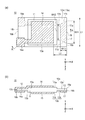
圧電振動片10は、図1に示すように、X方向に長辺、Z方向に短辺を有する矩形の板状の部材から形成されている。圧電振動片10には、振動部11と周辺部12とを有している。振動部11は、図1(a)に示すように、Y軸方向から見て、圧電振動片10の中央部分に形成されている。周辺部12は、図1(a)に示すように、Y方向から見て、振動部11を囲む領域に形成されている。
As shown in FIG. 1, the piezoelectric
振動部11は、図1(a)及び(b)に示すように、表面(+Y側の面)にメサ部13aが形成されている。メサ部13aは、周辺部12よりも+Y方向に高く形成されている。また、振動部11は、裏面(−Y側の面)にメサ部13bが形成されている。メサ部13bは、周辺部12よりも−Y方向に高く形成されている。このようなメサ部13a、13bを設けることにより、圧電振動片10の振動エネルギーを効率よく閉じ込めて、CI値(クリスタルインピーダンス値)を低減させることができる。なお、このようなメサ部13a、13bの一方又は両方は設けられなくてもよい。メサ部13aが設けられない場合、振動部11の表面は、周辺部12の表面(+Y側の面)12aと同一平面となる。また、メサ部13bが設けられない場合、振動部11の裏面は、周辺部12の裏面(−Y側の面)12bと同一平面となる。
As shown in FIGS. 1A and 1B, the vibrating
振動部11の表面には、励振電極14が設けられている。また、振動部11の裏面には、励振電極15が設けられている。励振電極14、15は、図1(a)に示すように、Y方向から見て、メサ部13a、13bの領域内に、矩形状に形成されている。励振電極14、15に所定の電圧が印加されることにより、振動部11は所定の振動数で振動する。
An
周辺部12の表面12aには、励振電極14から−X方向に引き出され、圧電振動片10の−X側の辺部16bまで引き出された引出電極14aが設けられている。引出電極14aは、周辺部12の−X側の側面12cを介して、周辺部12の裏面12bの−X側かつ+Z側の領域に引き出されている。引出電極14aは、励振電極14と電気的に接続されている。なお、図1では、−X側の側面12cに引出電極14aが形成されているが、+Z側の側面12cに引出電極14aが形成されてもよい。
On the
周辺部12の裏面12bには、励振電極15から−X方向に引き出された引出電極15aが設けられている。引出電極15aは、圧電振動片10の−X側の辺部16bまで形成されている。引出電極15aは、励振電極15と電気的に接続されている。
On the
周辺部12の裏面12b(圧電振動片10の裏面10b)には、指標マーク17が設けられている。指標マーク17の+X側の端部17aは、辺部18bの一部を含んで形成されている。なお、辺部18bは、圧電振動片10の裏面10bの+X側の短辺であり、引出電極15aが設けられた辺部16bの反対側(圧電振動片10の+X側)の辺部でもある。指標マーク17は、辺部18bの−Z側及び+Z側には形成されていない。指標マーク17は、接着剤153(図6等参照)の塗布位置を含むように、辺部18bから−X側に入り込んだ領域に設けられる。本実施形態では、接着剤153の塗布位置の一例として、辺部18bの中点19を含む領域に設定されている(図6(a)参照)。指標マーク17は、辺部18bの中点19を含む領域に設けられる。
An
指標マーク17は、図1(a)に示すように、+X側の端部17aと、−X側の端部17bと、外縁部17c、17dと、により囲まれた領域に形成されている。外縁部17cは、端部17aの−Z側の頂点と端部17bの−Z側の頂点とを結び、直線状に形成されている。また、外縁部17dは、端部17aの+Z側の頂点と端部17bの+Z側の頂点とを結び、直線状に形成されている。
As shown in FIG. 1A, the
指標マーク17は、辺部18bにおける幅(端部17aのZ軸方向の幅)W11が、中央側の幅(端部17bのZ軸方向の幅)W12よりも広く設定される。また、幅W11は、辺部18bの幅L1に対して例えば1/2〜4/5の長さに設定される。また、X軸方向の幅(端部17bから端部17aまでのX軸方向の距離)W13は、励振電極14、15から辺部18bまでのX軸方向の距離L2よりも短く設定されている。幅W13は、距離L2に対して例えば1/2以下に設定される。
The
指標マーク17は、Y軸方向から見ると、端部17bを上底、端部17aを下底、外縁部17c、17dを脚とし、幅W13を高さとする台形状に形成される。また、指標マーク17は、辺部18bの中点19を通るX軸方向の直線に対して対称に形成されている。指標マーク17の領域は、接着剤153が塗布可能となっている。
When viewed from the Y-axis direction, the
なお、指標マーク17は、上記した台形状に限定されない。例えば、外縁部17c、17dの一方又は両方が直線状であることに代えて曲線状としてもよい。また、指標マーク17は、中点19を通るX軸方向の直線に対して非対称に形成されてもよい。また、指標マーク17は、圧電振動片10の裏面10bに形成されることに代えて、表面10aに形成されてもよく、以下の第2〜第4実施形態においても同様である。この場合、指標マークは、圧電振動片10の表面(+Y側の面)の辺部18aの少なくとも一部を含むように形成される。
The
指標マーク17は、励振電極14、15や引出電極14a、15aと同様の導電性の金属膜であり、一体の金属膜として、同一の膜構成により形成されている。導電性の金属膜は、例えば、圧電振動片10である水晶材との密着性を確保するための下地膜としてニッケルタングステン(NiW)、ニッケル(Ni)、クロム(Cr)、チタン(Ti)、あるいはニッケルクロム(NiCr)や、ニッケルチタン(NiTi)が成膜され、その上に導電膜として金(Au)や銀(Ag)が成膜された積層構造が採用される。
The
また、励振電極14、15、引出電極14a、15a、及び指標マーク17の一部あるいは全てが、異なる膜構成あるいは異なる材料から形成されてもよい。例えば、指標マーク17は、下地膜または導電膜のうちいずれか一方の金属膜で形成されてもよい。また、指標マーク17は、非導電性の金属膜により形成されてもよい。また、指標マーク17は、金属膜であることに限定されず、例えば、樹脂やセラミックスが用いられたものや、圧電振動片10の表面性状を変えて反射率を変化させたもの、インク等を塗布して着色したものなどが用いられてもよい。なお、上記した指標マーク17の材質については、以下の第2〜第4実施形態においても同様である。
In addition, some or all of the
圧電振動片10は、例えば、裏面10bの引出電極14a、15a、及び指標マーク17上に、後述する導電性接着剤151、152、及び接着剤153が塗布され、接着剤151、152、及び153を介して後述するパッケージ110のベース130の表面(+Y側の面)131に接合される。これにより、圧電振動片10の−X側かつ−Z側の部分、−X側かつ+Z側の部分、及び+X側辺部18bの中点19の3箇所でベース130上において支持される(以下、3点支持という)。なお、圧電振動片10は、3点支持でベース130に保持されることに代えて、2点支持により保持されてもよい。2点支持では、引出電極14a、15aに導電性接着剤151、152を塗布し、指標マーク17上には接着剤153を塗布せずにベース130に接合される。2点支持では、圧電振動片10は、片持ち状態でベース130上に支持される。
In the piezoelectric vibrating
このように、第1実施形態によれば、辺部18bに指標マーク17が形成されるので圧電振動片10の外縁が容易に識別され、例えば、ベース130等との位置関係を容易に把握できる。例えば、圧電振動片10の画像をCCDやCMOS等のイメージセンサを持つ撮像装置で取得した場合、指標マーク17によって圧電振動片10の外縁を画像において識別可能となる。これにより、圧電振動片10が後述するベース130に搭載された際の搭載位置を画像等によって正確に判定することができる。
As described above, according to the first embodiment, since the
また、指標マーク17は、幅W11、W12、W13を有することにより、指標マーク17上において接着剤を塗布可能な領域を確実に確保できる。指標マーク17は、幅W11等を有するので、接着剤が塗布されても指標マーク17が隠れず、この指標マーク17と接着剤とを対比することにより、接着剤の塗布位置や塗布量が適切であるかについて容易に判別することができる。
Further, since the
また、指標マーク17は、励振電極14、15に近い端部17bの幅W12が端部17aの幅W11より狭く設定されるので、振動部11に対する振動特性に及ぼす影響を抑制できる。また、端部17aの幅W11を広くすることにより、辺部18bを広い範囲で認識することができる。
In addition, since the
また、指標マーク17が、圧電振動片10の裏面10bに代えて表面10aに形成された場合であっても、裏面10bに形成された場合と同様の効果を有する。なお、指標マーク17が裏面10bに形成された場合、裏面側に設けられた引出電極14a、15aと指標マーク17とはほぼ同一平面上に配置されるため、指標マーク17と撮像装置との距離は、引出電極14a、15aと撮像装置との距離と同一となり、撮像装置の焦点深度内にこれら指標マーク17等を容易に入れることができる。
Further, even when the
(圧電振動片10の製造方法)
次に、圧電振動片10の製造方法について説明する。
先ず、圧電ウェハが用意される。圧電振動片10は、圧電ウェハから個々の圧電振動片10を取り出す多面取りが行われる。圧電ウェハは、水晶結晶体からATカットにより所定の厚さで切り出される。続いて、圧電ウェハは、振動部を形成する部分に対してエッチングや切削等により厚さ(Y軸方向の幅)が薄くなるように形成され、振動部が所望の周波数特性を備えるように調整される。また、圧電振動片10の表面10a及び裏面10bには、フォトリソグラフィー法及びエッチングにより、メサ部13a、13bが形成される。続いて、圧電ウェハの表面10a、裏面10b、及び側面10cとなる位置に、励振電極14、15、引出電極14a、15a、及び指標マーク17が形成される。
(Method for manufacturing piezoelectric vibrating piece 10)
Next, a method for manufacturing the piezoelectric vibrating
First, a piezoelectric wafer is prepared. The piezoelectric vibrating
励振電極14、15、引出電極14a、15a、及び指標マーク17は、フォトリソグラフィー法及びエッチングにより導電性金属膜が成膜及びパターニングされて形成される。導電性金属膜は、先ず、圧電振動片10である水晶材との密着性を確保するための下地膜として、例えばニッケルタングステン(NiW)が成膜され、次いで、その上に導電膜として、例えば銀(Ag)が成膜される。次いで、エッチングによりパターニングされて各電極14等及び指標マーク17が形成される。
The
なお、励振電極14、15、引出電極14a、15a、及び指標マーク17は、このような導電性金属膜の成膜及パターニングにより、ほぼ同時に形成されるが、それぞれ別に形成されてもよい。また、パターニングされた導電性金属膜の形成は、フォトリソグラフィー法及びエッチングに代えて、メタルマスクを用いたスパッタリングや真空蒸着等により行われてもよい。このように各電極14等及び指標マーク17の形成後、圧電ウェハをスクライブラインに沿ってダイシングすることにより、個々の圧電振動片10が完成する。
The
このように、指標マーク17は、励振電極14、15及び引出電極14a、15aと同一の材料によりかつ同一の工程で形成することができる。これにより、圧電振動片10に指標マーク17を形成することにより生じる製造コストの増加を抑制することができる。
Thus, the
<第2実施形態>
次に、第2実施形態に係る圧電振動片20について、図2を用いて説明する。以下の説明において、第1実施形態と同一または同等の構成部分については同一符号を付けて説明を省略または簡略化する。本実施形態に係る圧電振動片20は、第1実施形態の指標マーク17に代えて指標マーク27が設けられている点で、図1に示す圧電振動片10とは異なる。
Second Embodiment
Next, the piezoelectric vibrating
圧電振動片20は、図2に示すように、周辺部12の裏面12bに指標マーク27が設けられている。指標マーク27の+X側の端部27aは、辺部18bの一部を含んで形成されている。指標マーク27は、辺部18bの−Z側及び+Z側には設けられていない。指標マーク27は、図1に示す指標マーク17と同様、接着剤153の塗布位置を含むように、辺部18bから−X側に入り込んだ領域に設けられる。本実施形態では、接着剤153の塗布位置は、辺部18bの中点19を含む領域に設定されている。指標マーク27は、辺部18bの中点19を含む領域に設けられる。
As shown in FIG. 2, the piezoelectric vibrating
指標マーク27は、図2に示すように、+X側の端部27aと、−X側の端部27bと、外縁部27c、27dと、により囲まれた領域に形成されている。外縁部27cは、端部27aの−Z側の頂点と端部27bとを結び、直線状に形成されている。外縁部27dは、端部27aの+Z側の頂点と端部27bの+Z側の頂点とを結び、直線状に形成されている。指標マーク27は、辺部18bにおける幅(端部27aのZ軸方向の幅)W21と、X軸方向の幅(端部27bから端部27aまでのX軸方向の距離)W23と、を有している。また、幅W21は、辺部18bの幅L1に対して例えば1/2〜4/5の長さに設定される。幅W23は、距離L2よりも短く設定される。幅W23は、距離L2に対して例えばL2の1/2以下に設定される。
As shown in FIG. 2, the
指標マーク27は、Y軸方向から見ると、−X側の端部26bを頂点、+X側の端部26aを底辺とした、幅W23を高さとする三角形状に形成される。また、指標マーク27は、辺部18bの中点19を通るX軸方向の直線に対して対称な形状に形成されている。また、指標マーク27の領域には、接着剤153が塗布可能となっている。なお、指標マーク27は、上記した形状に限定されない。例えば、外縁部27c、27dの一方又は両方が直線状であることに代えて曲線状としてもよい。また、指標マーク27は、中点19を通るX軸方向の直線に対して非対称に形成されてもよい。なお、指標マーク27は、励振電極14等と同様の導電性金属膜が用いられる点は、図1の指標マーク17と同様である。
When viewed from the Y-axis direction, the
このように、第2実施形態によれば、第1実施形態において示した効果と同様の効果を有する。さらに、指標マーク27は、中央側において幅(Z軸方向の長さ)を有しない構成であるため、振動部11の振動特性に対する影響をより確実に抑制することができる。なお、圧電振動片20の製造方法は、上記した圧電振動片10の製造方法とほぼ同様である。
Thus, according to the second embodiment, the same effects as those shown in the first embodiment are obtained. Furthermore, since the
<第3実施形態>
次に、第3実施形態に係る圧電振動片30について、図3を用いて説明する。以下の説明において、第1実施形態と同一または同等の構成部分については同一符号を付けて説明を省略または簡略化する。本実施形態に係る圧電振動片30は、第1実施形態の指標マーク17に代えて指標マーク37が設けられている点で、図1に示す圧電振動片10とは異なる。
<Third Embodiment>
Next, the piezoelectric vibrating
圧電振動片30は、図3に示すように、周辺部12の裏面12bに指標マーク37が設けられている。指標マーク37の+X側の端部37aは、辺部18bの一部を含んで形成されている。指標マーク37は、辺部18bの−Z側及び+Z側には設けられていない。指標マーク37は、図1に示す指標マーク17と同様、接着剤153の塗布位置を含む領域に設けられる。本実施形態では、接着剤153の塗布位置は、辺部18bの中点19を含む領域に設定されている。指標マーク37は、辺部18bの中点19を含む領域に設けられる。
As shown in FIG. 3, the piezoelectric vibrating
指標マーク37は、図3に示すように、+X側の端部37aと、−X側の端部37bと、外縁部37c、37dと、により囲まれた領域に形成されている。外縁部37cは、端部37aの−Z側の頂点と端部37bの−Z側の頂点とを結び、直線状に形成されている。外縁部37dは、端部37aの+Z側の頂点と端部37bの+Z側の頂点とを結び、直線状に形成されている。
As shown in FIG. 3, the
指標マーク37は、辺部18bにおける幅(端部37aのZ軸方向の幅)W31が、中央側の幅(端部37bのZ軸方向の幅)W32とほぼ同一の長さに設定される。また、幅W31は、辺部18bの幅L1に対して例えば1/2〜4/5の長さに設定される。また、X軸方向の幅(端部37bから端部37aまでのX軸方向の距離)W33は、距離L2よりも短く設定されている。幅W33は、距離L2に対して例えば1/2以下に設定される。
In the
指標マーク37は、Y軸方向からみると、−X側の端部37b及び+X側の端部37aを長辺、−Z側の外縁部37c及び+Z側の外縁部37dを短辺とする矩形状(長方形状)に形成される。また、指標マーク37は、辺部18bの中点19を通るX軸方向の直線に対して対称に形成されている。また、指標マーク37の領域は、接着剤153が塗布可能となっている。なお、指標マーク37は、上記した形状に限定されない。例えば、端部36b、外縁部37c、37dの一部又は全部が直線状であることに代えて曲線状としてもよい。また、指標マーク37は、中点19を通るX軸方向の直線に対して非対称に形成されてもよい。なお、指標マーク37は、励振電極14等と同様の導電性金属膜が用いられる点は、図1の指標マーク17と同様である。
When viewed from the Y-axis direction, the
このように、第3実施形態によれば、第1実施形態において示した効果と同様の効果を有する。さらに、指標マーク37の幅W32は、幅W31とほぼ同一に設定されるため、接着剤の塗布領域を広くすることができる。なお、圧電振動片30の製造方法は、上記した圧電振動片10の製造方法とほぼ同様である。
Thus, according to the third embodiment, the same effects as those shown in the first embodiment are obtained. Furthermore, since the width W32 of the
<第4実施形態>
次に、第4実施形態に係る圧電振動片40について、図4を用いて説明する。以下の説明において、第4実施形態と同一または同等の構成部分については同一符号を付けて説明を省略または簡略化する。本実施形態に係る圧電振動片40は、第1実施形態の指標マーク17に代えて指標マーク47が設けられている点で、図1に示す圧電振動片10とは異なる。
<Fourth embodiment>
Next, a piezoelectric vibrating
圧電振動片40は、図4に示すように、周辺部12の裏面12bに指標マーク47が設けられている。指標マーク47の+X側の端部47aは、辺部18bの全部を含んで形成されている。指標マーク47は、図1に示す指標マーク17と同様、接着剤153の塗布位置を含む領域に設けられる。本実施形態では、接着剤153の塗布位置は、辺部18bの中点19を含む領域に設定されている。指標マーク47は、辺部18bの中点19を含む領域に設けられる。
As shown in FIG. 4, the piezoelectric vibrating
指標マーク47は、図4に示すように、Y軸方向から見ると、図1に示す指標マーク17と同一の台形形状と、辺部18bに沿って幅(X軸方向の長さ)W43を持つ帯形状と、を組み合わせた領域に形成されている。指標マーク47の端部47bの幅W12は、図1の指標マーク17と同様の幅W12となっている。また、幅W13についても、図1の指標マーク17の幅W13と同様である。なお、幅W43の長さは任意に設定可能である。また、指標マーク47の領域は、接着剤153が塗布可能となっている。
As shown in FIG. 4, the
なお、指標マーク47は、上記した形状に限定されない。例えば、指標マーク47において、指標マーク17と同一の台形形状の部分を、第2または第3実施形態に係る指標マーク27、37の形状と置き換えて形成されてもよい。また、帯形状部分の幅W43は、Z軸方向に一定であることに限定されない。例えば、幅W43の±Z側の端部で幅を狭く(もしくは0とし)、中点19に向かって徐々に広くしたものでもよい。また、指標マーク47は、中点19を通るX軸方向の直線に対して非対称に形成されてもよい。なお、指標マーク37は、励振電極14等と同様の導電性金属膜が用いられる点は、図1の指標マーク17と同様である。
The
このように、第4実施形態によれば、第1実施形態において示した効果と同様の効果を有する。さらに、指標マーク47は辺部18bの全てを含む領域に形成されているため、圧電振動片40の辺部18bの全体を正確に識別することができる。一方、端部47bの幅W12が狭く設定されるので、振動部11に対する振動特性に及ぼす影響を抑制できる。なお、圧電振動片40の製造方法は、上記した圧電振動片10の製造方法とほぼ同様である。
Thus, according to the fourth embodiment, the same effects as those shown in the first embodiment are obtained. Furthermore, since the
<第5実施形態>
次に、第5実施形態に係る圧電振動片50について、図5を用いて説明する。以下の説明において、第1実施形態と同一または同等の構成部分については同一符号を付けて説明を省略または簡略化する。本実施形態に係る圧電振動片50は、第1実施形態の指標マーク17に代えて指標マーク57が設けられている点で、図1に示す圧電振動片10とは異なる。
<Fifth Embodiment>
Next, a piezoelectric vibrating
圧電振動片50は、図5に示すように、指標マーク57が設けられている。指標マーク57は、図1に示す指標マーク17と指標マーク57aとから構成される。指標マーク57aは、周辺部12の表面12aに形成されている。指標マーク17と指標マーク57aとは、Y軸方向から見てほぼ同一の台形状に形成され、圧電振動片50の厚さ(Y軸方向の長さ)の中心を含むXZ平面に対して対称に形成されている。従って、指標マーク57aは、上記した指標マーク17の端部17a、17bや、外縁部17c、17dのそれぞれと同一である。
As shown in FIG. 5, the piezoelectric vibrating
なお、指標マーク57は、上記した形状に限定されない。例えば、周辺部12の表面12a及び裏面12bにおいて、上記した第2〜第4実施形態の指標マーク27〜47の形態と同様のものが用いられてもよい。また、指標マーク17と指標マーク57aとが、同一形状かつ対称に形成されることに限定されない。例えば、指標マーク17と指標マーク57aとの形状が異なるものでもよい。また、指標マーク17と指標マーク57aとの配置がY軸方向から見てずれたものでもよい。なお、指標マーク57aは、励振電極14等と同様の導電性金属膜が用いられる点は、図1の指標マーク17と同様である。ただし、指標マーク17と指標マーク57aとで材質を変えてもよい。
The
このように、第5実施形態によれば、第1実施形態において示した効果と同様の効果を有する。さらに、圧電振動片50の表面10a及び裏面10bの両面に指標マークを有するので、圧電振動片50が非透過性の材質で形成された場合に、圧電振動片50の表面側から裏面の指標マーク17が見えないときでも指標マーク57aによって縁部を識別することができる。なお、圧電振動片50の製造方法は、上記した圧電振動片10の製造方法とほぼ同様であり、圧電振動片10の製造方法に加えて、指標マーク17と同時に指標マーク57aが形成される。
Thus, according to the fifth embodiment, the same effects as those shown in the first embodiment are obtained. Furthermore, since the index marks are provided on both the
<圧電デバイス>
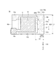
次に、圧電デバイス100の実施形態について説明する。以下の説明において、上記の実施形態と同一または同等の構成部分については同一符号を付けて説明を省略または簡略化する。なお、図6(a)では、リッド120の一部を透過して表わしている。この圧電デバイス100は、図6に示すように、圧電振動片10と、圧電振動片10を収容したパッケージ本体110とを有している。パッケージ本体110は、リッド120とベース130とを有している。リッド120及びベース130としては、ガラスが用いられるが、ガラスに代えて、シリコン、セラミックス、樹脂、金属等が用いられてもよい。
<Piezoelectric device>
Next, an embodiment of the
リッド120は、図6(b)に示すように、裏面(−Y側の面)の中央部分に凹部121が設けられ、この凹部121を囲むように接合面122が形成されている。なお、凹部121は、圧電振動片10を収容する空間として用いられる。
As shown in FIG. 6B, the
ベース130は、図6及び図7に示すように、板状であって、表面(+Y側の面)131には、接続電極132a、132b、引回電極133a、133b、及び対応マーク134が形成されている。引回電極133a、133bは、それぞれ接続電極132a、132bと電気的に接続される。対応マーク134は、圧電振動片10の指標マーク17に対応するように設けられており、圧電振動片10がパッケージ110に接着搭載される際に、指標マーク17と対応マーク134とを観察して、圧電振動片10の保持された位置を確認することが可能となっている。
As shown in FIGS. 6 and 7, the
接続電極132a、132b、引回電極133a、133b、及び対応マーク134は、例えばメタルマスク等を用いたスパッタリングや真空蒸着により導電性の金属膜が成膜されることで形成される。なお、フォトリソグラフィー法及びエッチングにより形成されてもよい。金属膜としては、圧電振動片10の励振電極14等と同様に、例えば、下地膜としてニッケルタングステン(NiW)を成膜し、その上に導電膜として銀(Ag)を成膜した積層構造が採用される。なお、下地膜は、クロム(Cr)や、チタン(Ti)、ニッケル(Ni)、あるいはニッケルクロム(NiCr)、ニッケルチタン(NiTi)などであってもよい。また、導電膜は、金(Au)などであってもよい。
The
また、対応マーク134は、接続電極132a、132bや引回電極133a、133bと同一の材質で形成されることに限定されない。例えば、対応マーク134は、下地膜または導電膜のうちいずれか一方の金属膜で形成されてもよい。また、対応マーク134は、非導電性の金属膜により形成されてもよい。また、対応マーク134は、金属膜であることに限定されず、例えば、樹脂やセラミックスが用いられたものや、ベース130の表面性状を変えて反射率を変化させたもの、インク等を塗布して着色したものなどが用いられてもよい
Further, the
ベース130の裏面(−Y側の面)135には、外部電極136a、136bが形成されている。外部電極136a、136bは、基板等への実装の際に一対の実装端子として用いられる。また、ベース130のZX平面における4つの角部には、角部を内側へ向けて曲面状に切り欠いたキャスタレーション137が設けられている。
−Xかつ+Z側の角部のキャスタレーション137の表面にはキャスタレーション電極138aが形成されている。このキャスタレーション電極138aを介して、引回電極133aと外部電極136aとは電気的に接続される。また、+Xかつ−Z側の角部のキャスタレーション137の表面にはキャスタレーション電極138cが形成されている。このキャスタレーション電極138cを介して、引回電極133bと外部電極136bとは電気的に接続される。
A
外部電極136a、136b及びキャスタレーション電極138a、138cは、接続電極132a等と同様に、例えばメタルマスク等を用いたスパッタリングや真空蒸着により導電性の金属膜が成膜されることで形成される。金属膜の膜構成については、接続電極132a等と同様である。金属膜は、フォトリソグラフィー法及びエッチングにより形成されてもよい。
The
リッド120とベース130とは、接合面122と表面131との間に配置された接合材154により接合される。なお、リッド120とベース130とは、直接接合されてもよい。圧電振動片10は、導電性接着剤151、152及び接着剤153により3点でベース130に保持される。導電性接着剤151は、引出電極14aと接続電極132aとの間に配置される。導電性接着剤152は、引出電極14bと接続電極132bとの間に配置される。接着剤153は、指標マーク17と対応マーク134との間に配置される。接着剤151により、引出電極15aと接続電極132aとが電気的に接続される。また、接着剤152により、引出電極14aと接続電極132bとが電気的に接続される。導電性接着剤151、152としては、シリコン系やポリイミド系の導電性接着剤が用いられる。
The
なお、接着剤153としては、導電性接着剤151、152と同様の導電性接着剤が使用されてもよく、また、非導電性の接着剤が使用されてもよい。また、接着剤153は、圧電振動片10の辺部18bの中央部分に配置されているがこれに限定されず、例えば、中央部分から±Z方向にずれた状態で配置されてもよい。また、圧電振動片10を3点で支持することに限定されず、接着剤153を配置せずに導電性接着剤151、152の2点で支持させてもよい。
As the adhesive 153, a conductive adhesive similar to the
圧電振動片10は、図6(b)に示すように、リッド120の凹部121とベース130の表面131とにより形成されたキャビティー111内に配置される。キャビティー111は、例えば真空雰囲気に設定されるが、これに限定されず、アルゴンガスや窒素ガスなどの不活性ガスが封入されてもよい。
As shown in FIG. 6B, the piezoelectric vibrating
このように、圧電デバイス100によれば、指標マーク17と対応マーク134との相対位置を確認することにより、圧電振動片10が適切な位置に保持されていることを容易に確認することができる。これにより、品質に優れかつ信頼性が向上した圧電デバイス100を提供することができる。なお、上記した実施形態では、第1実施形態の圧電振動片10が用いられているが、これに代えて第2〜5実施形態で説明した圧電振動片20、30、40、50が用いられてもよい。
As described above, according to the
さらに、変形例に係る圧電デバイス200、300について、図8を用いて説明する。以下の説明において、上記の実施形態と同一または同等の構成部分については同一符号を付けて説明を省略または簡略化する。図8(a)は、変形例に係る圧電デバイス200の断面図を示し、図8(b)は、他の変形例に係る圧電デバイス300の断面図を示している。
Furthermore, the
圧電デバイス200は、図8(a)に示すように、パッケージ210を有している。パッケージ210は、ベース130と、リッド221と、枠部222とから構成される。リッド221には、例えば、鉄、ニッケル、42アロイ、コバールなどの金属製の板状の部材が用いられる。枠部222は、圧電振動片10を収容する空間を形成するために用いられる。枠部222は、例えば、ベース130と同様に、ガラスが用いられるが、ガラスに代えて、シリコン、セラミックス、樹脂、金属等が用いられてもよい。
The
ベース130と枠部222とは、接合材154を介して接合される。なお、ベース130と枠部222とは、直接接合されてもよい。また、リッド221は、枠部222の+Y側から、例えばシーム溶接により銀(Ag)などのろう材を介して枠部222と接合される。なお、リッド221は、接合材を介して枠部222に接合されてもよい。
The
また、圧電デバイス300は、図8(b)に示すように、パッケージ310を有している。パッケージ310は、リッド320とベース330とから構成されている。リッド320は、図8(a)のリッド221と同様に、例えば、鉄、ニッケル、42アロイ、コバールなどの金属製の板状の部材が用いられる。ベース330は、図8(b)に示すように、表面(+Y側の面)の中央部分に凹部331が設けられ、この凹部331を囲むように接合面332が形成されている。なお、凹部331は、圧電振動片10を収容する空間として用いられる。
In addition, the
ベース330の凹部331の底面(+Y側の面)334には、圧電振動片10と導電性接合材151、152を介して接続される接続電極(不図示)と、この接続電極と電気的に接続された引回電極333a、333bとが形成されている。また、ベース330には、底面334と裏面(−Y側の面)335とを貫通する貫通孔337a、337bが設けられている。
A connection electrode (not shown) connected to the piezoelectric vibrating
貫通孔337a、337bのそれぞれは、底面334から裏面335にかけて徐々に口径が広がる円錐台状に形成されている。貫通孔337a、337b内には、貫通電極338a、338bがそれぞれ形成されている。この貫通電極338a、338bによって、引回電極333a、333bと外部電極336a、336bとは電気的に接続される。貫通電極338a、338bは、ベース130に設けられた貫通孔337a、337bを銅メッキ等により充填して形成される。
Each of the through
なお、上記した変形例に係る圧電デバイス200、300の構成を適宜組み合わせることも可能である。例えば、図8(a)の圧電デバイス200のベース130の電極として、図8(b)に示すような貫通電極338a、338bが設けられてもよい。また、圧電デバイスのパッケージとしては、図6及び図8に示す形態以外に、各種形態を適用可能である。
In addition, it is also possible to combine suitably the structure of the
(圧電デバイス100の製造方法)
次に、圧電デバイス100の製造方法について、図9〜図11を用いて説明する。以下の説明において、上記の実施形態と同一または同等の構成部分については同一符号を付けて説明を省略または簡略化する。なお、図9に示すフローチャートに沿って説明する。先ず、圧電振動片10を多面取りする圧電ウェハが用意される(ステップS01)。また、ベース130を多面取りするベースウェハBWが用意される(ステップS21)。リッド120を多面取りするリッドウェハLWが用意される(ステップS31)。その後、各ウェハが加工される。
(Method for Manufacturing Piezoelectric Device 100)
Next, a method for manufacturing the
ステップS01に続き、圧電ウェハの表面及び裏面は、振動部の厚さが調整されるとともに、メサ部13a、13bが形成される(ステップS02)。振動部の厚さの調整やメサ部13a等の形成は、例えば、フォトリソグラフィー法及びエッチングが用いられる。ただし、フォトリソグラフィー法及びエッチングに代えて、切削等の機械的加工が用いられてもよい。
Subsequent to step S01, the thickness and the
次に、圧電ウェハの表面及び裏面に、励振電極14、15及び電極14a、15aが形成される。同時に、圧電ウェハの裏面に指標マーク17が形成される(ステップS03)。これら励振電極14等は、例えば、フォトリソグラフィー法及びエッチングが用いられる。ただし、励振電極14等の形成は、メタルマスクを用いたスパッタリングや真空蒸着等が用いられてもよい。なお、圧電振動片10の側面12cに対する引出電極14a(図1参照)は、例えば、予め圧電ウェハに形成された貫通穴の内周面に導電性金属膜を成膜して形成される。次に、予め設定されたスクライブラインに沿って圧電ウェハが切断され、個々の圧電振動片10が形成される(形成工程、ステップS04)。
Next,
一方、ベースウェハBWは、ステップS21に続き、貫通孔160及び各種電極が形成される(ステップS22)。図10(a)に示すように、ベースウェハBWは、円形の断面を有する貫通孔160が形成される。この貫通孔160は、圧電デバイス100においてキャスタレーション137を形成するものである。貫通孔160は、例えばフォトリソグラフィー法及びエッチングにより形成されるが、切削等の機械的加工により形成されてもよい。
On the other hand, in the base wafer BW, subsequent to step S21, the through
また、ベースウェハBWの表面(+Y側の面)には、接続電極132a、132b、引回電極133a、133bが形成される。同時に、ベースウェハBWの表面に対応マーク134が形成される。また、貫通孔160の側面には、キャスタレーション電極138a等が形成される。また、ベースウェハBWの裏面(−Y側の面)には、外部電極136a、136bが形成される。
In addition,
リッドウェハLWは、ステップS31に続き、図10(b)に示すように、裏面(−Y側の面)に凹部121が形成される(ステップS32)。凹部121は、例えばフォトリソグラフィー法及びエッチングにより形成されるが、切削等の機械的加工により形成されてもよい。
In step S31, the lid wafer LW is formed with a
次に、図9に示すように、ステップS04に続き、個々の圧電振動片10を取り出すとともに、例えばカメラ等の撮像装置により圧電振動片10の画像を取得し、圧電振動片10の形状を認識する(ステップS05)。なお、圧電振動片10の取り出しは、ロボットハンド等の各種マニピュレータが用いられてもよい。
Next, as shown in FIG. 9, following step S <b> 04, each piezoelectric vibrating
次に、圧電振動片10の所定箇所に導電性接着剤が塗布される(ステップS06)。図11(c)に示すように、ステップS05により認識した圧電振動片10の形状を用いて、圧電振動片10の裏面10bの引出電極14a、15aに導電性接着剤151、152が塗布され、指標マーク17に接着剤153が塗布される。なお、接着剤153は、導電性接着剤でもよい点は上述のとおりである。また、導電性接着剤151等の塗布は、予め配置された3本のノズルからそれぞれ接着剤を吐出させるものや、1本のノズルが3か所を移動して順次接着剤を吐出させるものなどが用いられる。また、図11(c)では、接着剤153が指標マーク17からはみ出すように塗布されているが、これに限定されず、接着剤153が指標マーク17内に入るように塗布されてもよい。また、指標マーク17に接着剤153が塗布されなくてもよい。
Next, a conductive adhesive is applied to a predetermined portion of the piezoelectric vibrating piece 10 (step S06). As shown in FIG. 11C,
次に、導電性接着剤151、152及び接着剤153の確認が行われる(塗布確認工程、ステップS07)。導電性接着剤151等の確認は、例えばカメラ等の撮像装置により圧電振動片10の画像を取得することにより行う。なお、この撮像装置は、先に説明した圧電振動片10の形状を認識する際に使用した撮像装置が用いられてもよい。撮像装置により取得した画像に基づいて、導電性接着剤151等の塗布位置及び塗布量が確認される。なお、塗布量は、導電性接着剤151等の大きさ(画像での面積)によって判断される。
Next, the
また、ステップS07において、接着剤153は、指標マーク17と対比されることにより、塗布位置や塗布量が確認される。このとき、圧電振動片10が透明であっても指標マーク17を画像で確認でき、この指標マーク17との対比を行うことにより、接着剤153の塗布位置や塗布量を正確に確認することができる。なお、導電性接着剤151等の塗布位置や塗布量が不適切と判断された場合は、その部分のリペアが試みられるか、または、その圧電振動片10を除去して、次の圧電振動片10の載置が進められる。
In step S07, the adhesive 153 is compared with the
次に、導電性接着剤151等が塗布された圧電振動片10は、図11(d)に示すように、ステップS22を経たベースウェハBWに載置される(ステップS07)。これにより、圧電振動片10は、導電性接着剤151等を介してベースウェハBWに保持される。なお、ベースウェハBWへの圧電振動片10の載置は、予め移動量が設定されたマニュピレータ等によって行ってもよく、また、撮像装置で画像を見ながら行ってもよい。撮像装置の画像を用いる場合、圧電振動片10の指標マーク17とベースウェハBWの対応マーク134とを対比しながら圧電振動片10の載置を行ってもよい。
Next, as shown in FIG. 11D, the piezoelectric vibrating
なお、接着剤153は、上記したステップS06において、指標マーク17からはみ出した状態で塗布されている。従って、圧電振動片10がベースウェハBWに載置されると、図11(d)に示すように、対応マーク134上に接着剤153がはみ出した状態となる。これにより、撮像装置の画像から接着剤153の存在を確認することができる。
The adhesive 153 is applied in a state of protruding from the
次に、ベースウェハBWに対して圧電振動片10が適切に搭載されているか検査が行われる(確認工程、ステップS09)。この検査は、例えば撮像装置によって取得した画像により判断される。また、この検査は、圧電振動片10の指標マーク17とベースウェハBWに設けられた対応マーク134との相対的な位置関係を観察し、圧電振動片10が保持された位置を確認することにより行われる。なお、ベースウェハBWに対する圧電振動片10の位置が不適切と判断された場合は、その部分についてステップS05に戻り、再度圧電振動片10の載置を試みるか、または、その部分の圧電デバイスを不良と記録してその後の処理が進められる。
Next, it is inspected whether the piezoelectric vibrating
次に、圧電振動片10が搭載されたベースウェハBWは、接合材154を介して、ステップS32を経たリッドウェハLWと接合される(保持工程、ステップS10)。ベースウェハBWとリッドウェハLWとの接合は、例えば真空雰囲気や、窒素ガス等の不活性ガス雰囲気において行われる。その後、接合されたウェハは、ダイシングソーなどにより、スクライブラインSLに沿って切断され、個々の圧電デバイス100が完成する。
Next, the base wafer BW on which the piezoelectric vibrating
このように、圧電デバイス100の製造方法によれば、接着剤153は、指標マーク17と対比されることにより、塗布位置や塗布量を容易に確認できる。さらに、圧電振動片10がベースウェハBW(ベース130)に載置された際、指標マーク17と対応マーク134とを対比することにより、ベースウェハBWに対する圧電振動片10の相対位置を容易に確認できる。これにより、製造時の圧電振動片10の搭載不良による不良品の発生を抑制し、品質がよくかつ信頼性の高い圧電デバイス100を提供することができる。
As described above, according to the method for manufacturing the
なお、図9に示すステップの一部は省略されてもよい。また、上記したベースウェハBWの加工工程(ステップS22)や、リッドウェハLWの加工工程(ステップS32)は、圧電ウェハの加工工程(ステップS02〜S04等)と並行して行われてもよい。この場合、圧電デバイス100の製造時間が短縮されて製造コストが低減される。また、図9〜図11では、図6に示す圧電デバイス100の製造方法を示しているが、図8に示す圧電デバイス200、300の製造方法についても、ベースウェハBWの加工を除いてほぼ同様である。
Note that some of the steps shown in FIG. 9 may be omitted. Further, the above-described processing step of the base wafer BW (Step S22) and the processing step of the lid wafer LW (Step S32) may be performed in parallel with the processing steps of the piezoelectric wafer (Steps S02 to S04, etc.). In this case, the manufacturing time of the
以上、本発明の圧電振動片、圧電デバイス、及び圧電デバイスの製造方法について説明したが、本発明は、上記した説明に限定されるものではなく、本発明の要旨を逸脱しない範囲において種々の変更が可能である。 The piezoelectric vibrating piece, the piezoelectric device, and the manufacturing method of the piezoelectric device of the present invention have been described above. However, the present invention is not limited to the above description, and various modifications can be made without departing from the gist of the present invention. Is possible.
例えば、上記した各実施形態において、圧電振動片10等としては、ATカットの水晶振動片に限定されず、BTカットやGTカットや、XTカットなどの水晶片が用いられてもよく、音叉型の水晶振動片であってもよい。また、圧電振動片10として、水晶振動片に限定されず、タンタル酸リチウムやニオブ酸リチウムなどが用いられてもよい。また、圧電デバイス100として圧電振動子を示しているが、発振器であってもよい。発振器の場合は、ベース120にIC等が搭載され、圧電振動片10の引出電極14a等、及びベース130の外部電極136a等がそれぞれICに接続される。
For example, in each of the embodiments described above, the piezoelectric vibrating
10、20、30、40、50…圧電振動片
10a…表面
10b…裏面
11…振動部
14、15…励振電極
14a、15a…引出電極
16b、18a、18b…辺部
17、27、37、47、57、57a…指標マーク
100、200、300…圧電デバイス
134…対応マーク
153…接着剤
DESCRIPTION OF
Claims (7)
前記圧電振動片の表面及び裏面の少なくとも一方に、前記一方の辺部の反対側の辺部の少なくとも一部を含み、かつ、接着剤を塗布可能な領域に指標マークが形成され、
前記指標マークは、前記反対側の辺部の中点を含む領域に形成され、前記中点から前記一方の辺部に向かう方向に前記接着剤を塗布可能な幅を有し、前記反対側の辺部における幅が中央側の幅より広くなるように形成される圧電振動片。 In a piezoelectric vibrating piece comprising an excitation electrode formed on a vibration part, and an extraction electrode drawn from the excitation electrode to one side,
In at least one of the front and back surfaces of the piezoelectric vibrating piece, including at least a part of a side opposite to the one side, and an index mark is formed in a region where an adhesive can be applied ,
The index mark is formed in a region including a midpoint of the opposite side portion, and has a width that allows the adhesive to be applied in a direction from the midpoint toward the one side portion. A piezoelectric vibrating piece formed such that the width at the side portion is wider than the width at the center side .
前記圧電振動片の表面及び裏面の少なくとも一方に、前記一方の辺部の反対側の辺部の少なくとも一部を含み、かつ、接着剤を塗布可能な領域に指標マークが形成され、
前記指標マークは、前記圧電振動片の厚さ方向から見た際に前記接着剤の塗布位置を一部に含みかつ前記反対側の辺部の中点を含む領域に形成され、前記中点から前記一方の辺部に向かう方向に前記接着剤を塗布可能な幅を有し、前記反対側の辺部における幅が中央側の幅より広くなるように形成される圧電振動片。 In a piezoelectric vibrating piece comprising an excitation electrode formed on a vibration part, and an extraction electrode drawn from the excitation electrode to one side,
In at least one of the front and back surfaces of the piezoelectric vibrating piece, including at least a part of a side opposite to the one side, and an index mark is formed in a region where an adhesive can be applied ,
The index mark is formed in a region including a part of the adhesive application position and a midpoint of the opposite side when viewed from the thickness direction of the piezoelectric vibrating piece, from the midpoint A piezoelectric vibrating piece having a width in which the adhesive can be applied in a direction toward the one side, and a width at the opposite side being wider than a width at the center .
前記ベースは、前記圧電振動片の前記指標マークに対応する対応マークを備える圧電デバイス。 A piezoelectric device having a base for holding the piezoelectric vibrating piece according to any one of claims 1 to 5,
The base includes a piezoelectric device including a corresponding mark corresponding to the index mark of the piezoelectric vibrating piece.
前記圧電振動片をベースに保持させる保持工程と、
前記圧電振動片の前記指標マークと、前記ベースに設けられた対応マークとを観察して前記圧電振動片が保持された位置を確認する確認工程と、を含み、
前記保持工程は、前記圧電振動片の裏面において前記圧電振動片の厚さ方向から見た際の前記指標マークの領域の一部に接着剤を塗布し、前記接着剤と前記指標マークとを対比して前記接着剤の塗布位置を確認する塗布確認工程を含む圧電デバイスの製造方法。 A forming step of forming the piezoelectric vibrating piece according to any one of claims 1 to 5,
A holding step of holding the piezoelectric vibrating piece on a base;
Wherein said index mark of the piezoelectric vibrating piece, seen including a confirmation step, in which the piezoelectric vibrating piece by observing the corresponding mark provided on the base to check the stored position,
In the holding step, an adhesive is applied to a part of the area of the index mark when viewed from the thickness direction of the piezoelectric vibrating piece on the back surface of the piezoelectric vibrating piece, and the adhesive and the index mark are compared. method of manufacturing including the piezoelectric device a coating confirmation step of confirming application position of the adhesive is.
Priority Applications (4)
| Application Number | Priority Date | Filing Date | Title |
|---|---|---|---|
| JP2013123740A JP6133697B2 (en) | 2013-06-12 | 2013-06-12 | Piezoelectric vibrating piece, piezoelectric device, and method of manufacturing piezoelectric device |
| US14/295,354 US20140368089A1 (en) | 2013-06-12 | 2014-06-04 | Piezoelectric vibrating piece, piezoelectric device, and method for fabricating the piezoelectric device |
| CN201410256413.6A CN104242857A (en) | 2013-06-12 | 2014-06-10 | Piezoelectric vibrating piece, piezoelectric device, and method for fabricating the piezoelectric device |
| TW103120113A TW201448460A (en) | 2013-06-12 | 2014-06-11 | Piezoelectric vibrating piece, piezoelectric device, and method for fabricating the piezoelectric device |
Applications Claiming Priority (1)
| Application Number | Priority Date | Filing Date | Title |
|---|---|---|---|
| JP2013123740A JP6133697B2 (en) | 2013-06-12 | 2013-06-12 | Piezoelectric vibrating piece, piezoelectric device, and method of manufacturing piezoelectric device |
Publications (2)
| Publication Number | Publication Date |
|---|---|
| JP2014241539A JP2014241539A (en) | 2014-12-25 |
| JP6133697B2 true JP6133697B2 (en) | 2017-05-24 |
Family
ID=52018639
Family Applications (1)
| Application Number | Title | Priority Date | Filing Date |
|---|---|---|---|
| JP2013123740A Expired - Fee Related JP6133697B2 (en) | 2013-06-12 | 2013-06-12 | Piezoelectric vibrating piece, piezoelectric device, and method of manufacturing piezoelectric device |
Country Status (4)
| Country | Link |
|---|---|
| US (1) | US20140368089A1 (en) |
| JP (1) | JP6133697B2 (en) |
| CN (1) | CN104242857A (en) |
| TW (1) | TW201448460A (en) |
Families Citing this family (14)
| Publication number | Priority date | Publication date | Assignee | Title |
|---|---|---|---|---|
| JP6110112B2 (en) * | 2012-11-19 | 2017-04-05 | 日本電波工業株式会社 | Piezoelectric device |
| JP2014176071A (en) * | 2013-03-13 | 2014-09-22 | Nippon Dempa Kogyo Co Ltd | Piezoelectric vibration piece and piezoelectric device |
| JP6338367B2 (en) * | 2013-12-24 | 2018-06-06 | 日本電波工業株式会社 | Crystal oscillator |
| US10804877B2 (en) * | 2014-01-21 | 2020-10-13 | Avago Technologies International Sales Pte. Limited | Film bulk acoustic wave resonator (FBAR) having stress-relief |
| CN106233619B (en) * | 2014-04-25 | 2019-04-09 | 株式会社村田制作所 | Crystal Vibration Device |
| WO2016067924A1 (en) * | 2014-10-27 | 2016-05-06 | 株式会社村田製作所 | Piezoelectric device and method for manufacturing piezoelectric device |
| US9503048B2 (en) * | 2014-11-21 | 2016-11-22 | Sii Crystal Technology Inc. | Piezoelectric vibrating reed and piezoelectric vibrator |
| KR102029502B1 (en) * | 2014-12-04 | 2019-10-07 | 삼성전기주식회사 | Crystal oscillator package |
| JP2016178404A (en) * | 2015-03-19 | 2016-10-06 | セイコーエプソン株式会社 | Method for manufacturing vibrator and method for manufacturing oscillator |
| CN108141194B (en) * | 2015-10-02 | 2021-07-06 | 株式会社村田制作所 | Crystal plate and crystal oscillator |
| TWI630737B (en) | 2015-10-08 | 2018-07-21 | 村田製作所股份有限公司 | Crystal vibrating element and crystal vibrator having the crystal vibrating element |
| JP7135576B2 (en) * | 2018-08-17 | 2022-09-13 | セイコーエプソン株式会社 | Vibrating device, manufacturing method of vibrating device, electronic device and moving object |
| JP7247641B2 (en) * | 2019-02-21 | 2023-03-29 | セイコーエプソン株式会社 | Vibration element, vibration device, electronic equipment and moving body |
| JPWO2021059576A1 (en) * | 2019-09-25 | 2021-04-01 |
Family Cites Families (10)
| Publication number | Priority date | Publication date | Assignee | Title |
|---|---|---|---|---|
| JP2003069370A (en) * | 2001-08-29 | 2003-03-07 | Miyota Kk | Piezoelectric vibrator and its manufacturing method |
| JP2008206002A (en) * | 2007-02-22 | 2008-09-04 | Epson Toyocom Corp | Package and piezoelectric device using the same |
| JP2008306352A (en) * | 2007-06-06 | 2008-12-18 | Epson Toyocom Corp | Mounting inspection method of piezoelectric vibrating piece made of quartz substrate, and piezoelectric vibrating piece according to the mounting inspection |
| JP4990047B2 (en) * | 2007-07-02 | 2012-08-01 | 日本電波工業株式会社 | Piezoelectric vibrating piece and piezoelectric device |
| JP5216290B2 (en) * | 2007-09-27 | 2013-06-19 | 日本電波工業株式会社 | Piezoelectric device and method for manufacturing piezoelectric device |
| US7915791B2 (en) * | 2007-10-18 | 2011-03-29 | Nihon Dempa Kogyo Co., Ltd. | Quartz crystal device accomodating crystal blanks of multiple shapes and sizes |
| JP5234506B2 (en) * | 2008-09-29 | 2013-07-10 | セイコーエプソン株式会社 | Vibrator |
| JP4709884B2 (en) * | 2008-09-29 | 2011-06-29 | 日本電波工業株式会社 | Piezoelectric vibrating piece and piezoelectric device |
| JP4988799B2 (en) * | 2009-09-16 | 2012-08-01 | 日本電波工業株式会社 | Piezoelectric vibration device and method for manufacturing piezoelectric vibration device |
| JP5751949B2 (en) * | 2011-06-17 | 2015-07-22 | 京セラクリスタルデバイス株式会社 | Piezoelectric vibration element and piezoelectric device |
-
2013
- 2013-06-12 JP JP2013123740A patent/JP6133697B2/en not_active Expired - Fee Related
-
2014
- 2014-06-04 US US14/295,354 patent/US20140368089A1/en not_active Abandoned
- 2014-06-10 CN CN201410256413.6A patent/CN104242857A/en active Pending
- 2014-06-11 TW TW103120113A patent/TW201448460A/en unknown
Also Published As
| Publication number | Publication date |
|---|---|
| CN104242857A (en) | 2014-12-24 |
| TW201448460A (en) | 2014-12-16 |
| US20140368089A1 (en) | 2014-12-18 |
| JP2014241539A (en) | 2014-12-25 |
Similar Documents
| Publication | Publication Date | Title |
|---|---|---|
| JP6133697B2 (en) | Piezoelectric vibrating piece, piezoelectric device, and method of manufacturing piezoelectric device | |
| CN106169917B (en) | Method for manufacturing piezoelectric vibrating reed, and piezoelectric vibrator | |
| JP2009165006A (en) | Piezoelectric vibrating piece, piezoelectric device, and tuning fork type piezoelectric vibrator frequency adjusting method | |
| JP2018148380A (en) | Piezoelectric vibrating piece and method for manufacturing the piezoelectric vibrating piece | |
| JP5181938B2 (en) | Tuning fork crystal unit | |
| JP5054146B2 (en) | Piezoelectric device and manufacturing method thereof | |
| JP2011193436A (en) | Tuning fork crystal resonator chip, tuning fork crystal resonator, and method of manufacturing the tuning fork crystal resonator chip | |
| JP6716283B2 (en) | Piezoelectric vibrating piece and piezoelectric vibrator | |
| CN120729211A (en) | Piezoelectric vibrating piece, piezoelectric vibrator, and method for manufacturing the same | |
| JP2015177335A (en) | Piezoelectric device package, and piezoelectric device | |
| JP7079607B2 (en) | Piezoelectric vibrating pieces, piezoelectric vibrators, and manufacturing methods | |
| CN107342745A (en) | Piezoelectric patches, piezoelectric vibration device, the manufacture method of piezoelectric vibrating device and piezoelectric patches | |
| JP2016032195A (en) | Piezoelectric vibrating piece, method for manufacturing piezoelectric vibrating piece, and piezoelectric device | |
| JP2015177480A (en) | Manufacturing method of piezoelectric vibration piece, piezoelectric vibration piece, and piezoelectric device | |
| JP7232574B2 (en) | Method for manufacturing piezoelectric vibrating piece and method for manufacturing piezoelectric vibrator | |
| CN109891743B (en) | Tuning fork type vibrating piece, tuning fork type vibrator and manufacturing method thereof | |
| CN107888161B (en) | Wafer, piezoelectric vibrating reed, and piezoelectric vibrator | |
| JP2018082400A (en) | Piezoelectric vibration piece and piezoelectric vibrator | |
| JP6436175B2 (en) | Tuning fork type vibrator | |
| JP2015173408A (en) | Piezoelectric vibration piece, manufacturing method of the same, and piezoelectric device | |
| JP2015023387A (en) | Piezoelectric device | |
| JP6506535B2 (en) | Piezoelectric vibrating reed and piezoelectric vibrator | |
| WO2015115388A1 (en) | Piezoelectric device package and piezoelectric device | |
| JP2014175900A (en) | Piezoelectric vibration piece, piezoelectric vibration piece manufacturing method, and piezoelectric device | |
| JP2014192802A (en) | Piezoelectric vibration piece, process of manufacturing the same, and piezoelectric device |
Legal Events
| Date | Code | Title | Description |
|---|---|---|---|
| A621 | Written request for application examination |
Free format text: JAPANESE INTERMEDIATE CODE: A621 Effective date: 20160210 |
|
| A977 | Report on retrieval |
Free format text: JAPANESE INTERMEDIATE CODE: A971007 Effective date: 20161111 |
|
| A131 | Notification of reasons for refusal |
Free format text: JAPANESE INTERMEDIATE CODE: A131 Effective date: 20161121 |
|
| A601 | Written request for extension of time |
Free format text: JAPANESE INTERMEDIATE CODE: A601 Effective date: 20170116 |
|
| A521 | Request for written amendment filed |
Free format text: JAPANESE INTERMEDIATE CODE: A523 Effective date: 20170321 |
|
| TRDD | Decision of grant or rejection written | ||
| A01 | Written decision to grant a patent or to grant a registration (utility model) |
Free format text: JAPANESE INTERMEDIATE CODE: A01 Effective date: 20170417 |
|
| A61 | First payment of annual fees (during grant procedure) |
Free format text: JAPANESE INTERMEDIATE CODE: A61 Effective date: 20170420 |
|
| R150 | Certificate of patent or registration of utility model |
Ref document number: 6133697 Country of ref document: JP Free format text: JAPANESE INTERMEDIATE CODE: R150 |
|
| R250 | Receipt of annual fees |
Free format text: JAPANESE INTERMEDIATE CODE: R250 |
|
| R250 | Receipt of annual fees |
Free format text: JAPANESE INTERMEDIATE CODE: R250 |
|
| R250 | Receipt of annual fees |
Free format text: JAPANESE INTERMEDIATE CODE: R250 |
|
| LAPS | Cancellation because of no payment of annual fees |