JP6126211B2 - Reinitialization of processing system from volatile memory when resuming from low power state - Google Patents
Reinitialization of processing system from volatile memory when resuming from low power state Download PDFInfo
- Publication number
- JP6126211B2 JP6126211B2 JP2015515142A JP2015515142A JP6126211B2 JP 6126211 B2 JP6126211 B2 JP 6126211B2 JP 2015515142 A JP2015515142 A JP 2015515142A JP 2015515142 A JP2015515142 A JP 2015515142A JP 6126211 B2 JP6126211 B2 JP 6126211B2
- Authority
- JP
- Japan
- Prior art keywords
- configuration information
- processor
- boot
- processor device
- volatile memory
- Prior art date
- Legal status (The legal status is an assumption and is not a legal conclusion. Google has not performed a legal analysis and makes no representation as to the accuracy of the status listed.)
- Active
Links
- 238000012545 processing Methods 0.000 title description 41
- 238000000034 method Methods 0.000 claims description 49
- 230000007958 sleep Effects 0.000 claims description 28
- 230000004044 response Effects 0.000 claims description 14
- 238000012546 transfer Methods 0.000 claims description 6
- 238000013507 mapping Methods 0.000 claims description 4
- 230000008569 process Effects 0.000 description 27
- 238000004519 manufacturing process Methods 0.000 description 13
- 238000013461 design Methods 0.000 description 10
- 230000002093 peripheral effect Effects 0.000 description 9
- 230000008901 benefit Effects 0.000 description 7
- 238000010586 diagram Methods 0.000 description 5
- 238000012360 testing method Methods 0.000 description 5
- 230000015572 biosynthetic process Effects 0.000 description 3
- 238000004088 simulation Methods 0.000 description 3
- 238000003786 synthesis reaction Methods 0.000 description 3
- 238000012795 verification Methods 0.000 description 3
- 238000011960 computer-aided design Methods 0.000 description 2
- 230000006266 hibernation Effects 0.000 description 2
- 238000012986 modification Methods 0.000 description 2
- 230000004048 modification Effects 0.000 description 2
- 230000003287 optical effect Effects 0.000 description 2
- 230000011664 signaling Effects 0.000 description 2
- 230000001360 synchronised effect Effects 0.000 description 2
- 230000006399 behavior Effects 0.000 description 1
- 239000003990 capacitor Substances 0.000 description 1
- 230000008859 change Effects 0.000 description 1
- 238000012942 design verification Methods 0.000 description 1
- 238000005516 engineering process Methods 0.000 description 1
- 230000006870 function Effects 0.000 description 1
- 230000006872 improvement Effects 0.000 description 1
- 230000000977 initiatory effect Effects 0.000 description 1
- 230000003068 static effect Effects 0.000 description 1
- 239000000725 suspension Substances 0.000 description 1
Images


Classifications
-
- G—PHYSICS
- G06—COMPUTING; CALCULATING OR COUNTING
- G06F—ELECTRIC DIGITAL DATA PROCESSING
- G06F9/00—Arrangements for program control, e.g. control units
- G06F9/06—Arrangements for program control, e.g. control units using stored programs, i.e. using an internal store of processing equipment to receive or retain programs
- G06F9/44—Arrangements for executing specific programs
- G06F9/4401—Bootstrapping
- G06F9/4418—Suspend and resume; Hibernate and awake
-
- G—PHYSICS
- G06—COMPUTING; CALCULATING OR COUNTING
- G06F—ELECTRIC DIGITAL DATA PROCESSING
- G06F1/00—Details not covered by groups G06F3/00 - G06F13/00 and G06F21/00
- G06F1/26—Power supply means, e.g. regulation thereof
- G06F1/32—Means for saving power
Landscapes
- Engineering & Computer Science (AREA)
- Theoretical Computer Science (AREA)
- Software Systems (AREA)
- Physics & Mathematics (AREA)
- General Engineering & Computer Science (AREA)
- General Physics & Mathematics (AREA)
- Computer Security & Cryptography (AREA)
- Stored Programmes (AREA)
- Power Sources (AREA)
Description
本開示は、概して処理システムに関し、より詳細には、処理システムの電力状態の移行に関する。 The present disclosure relates generally to processing systems, and more particularly to transitioning power states of processing systems.
処理システムは、比較的不活性な期間における電力消費を低減するために、1つ以上のスリープ状態を実行することが多い。このようなスリープ状態のいくつかは、プロセッサ装置の1つ以上の構成要素またはプロセッサ装置全体の電力を除去することを含み、オペレーティングシステムが制御をレジュームする前にスリープ状態を終了する際に、プロセッサ装置の再初期化を必要とする。従来の再初期化は、パワーオンリセットからの初期化と同様に実行されており、プロセッサ装置の外部の不揮発性メモリからアクセスされる基本入力/出力システム(BIOS)コードの実行を含む「コールドブート」とも称されている。不揮発性メモリからBIOSコードへのアクセスは、比較的低速であるため、このようなスリープ状態を終了する際に従来の処理システムで見られる比較的長いウェークアップ時間(wake−up latency)の主な原因となる。 Processing systems often execute one or more sleep states to reduce power consumption during relatively inactive periods. Some of such sleep states include removing power of one or more components of the processor device or the entire processor device, and the processor upon exiting the sleep state before the operating system resumes control. Requires reinitialization of the device. Conventional re-initialization is performed in the same way as initialization from a power-on reset and includes the execution of basic input / output system (BIOS) code accessed from non-volatile memory external to the processor unit. Is also called. Access to the BIOS code from non-volatile memory is relatively slow, so the main cause of the relatively long wake-up latency found in conventional processing systems when exiting such a sleep state It becomes.
本開示は、添付図面を参照することによって理解を深めることができ、多くの特徴および利点が当業者にとって自明となるであろう。 The present disclosure can be better understood with reference to the following drawings, and many features and advantages will be apparent to those skilled in the art.
異なる図面で用いられる同一の参照符号は、類似または同一の項目を示す。 The same reference numbers used in different drawings indicate similar or identical items.
図1〜4は、揮発性メモリへの電力が維持されている一方でプロセッサ装置がパワーダウンしている低電力状態から処理システムを効率的にレジューム(再開)するための技術の例を示す。一実施形態では、レジュームブート構成情報は、パワーオンリセットまたは他のコールドブート状態からの処理システムのブートプロセスの一部として、揮発性メモリに記憶されている。プロセッサ装置は、低電力状態を開始するというインジケータがアサートされると、揮発性メモリが記憶された情報を保持できるように少なくとも最低電圧が揮発性メモリに供給されている間、パワーダウンされる。プロセッサ装置のレジュームコントローラは、低電力状態を終了または再開するというインジケータを受信すると、不揮発性メモリからメモリコントローラに関する構成情報にアクセスするとともに、メモリコントローラを介して揮発性メモリにアクセスできるように、構成情報を用いてメモリコントローラを構成または他の方法で復元する。その後、プロセッサ装置は、低電力状態中に揮発性メモリによって保持されるコア状態情報であって、構成されたメモリコントローラを介してアクセスされるコア状態情報を用いて、1つ以上のプロセッサコアの最初のコンテキストまたは状態を構成することができる。1つ以上のプロセッサコアは、低電力状態中に揮発性メモリによって保持されるレジュームブートコードであって、構成されたメモリコントローラを介してアクセスされるレジュームブートコードを実行することによって、ブートプロセスを完了することができる。低電力状態からのレジュームプロセスの間、揮発性メモリからコア状態情報およびレジュームブートコードにアクセスすることによって、不揮発性メモリからアクセスされるブートコードおよび他のブート情報に依存する従来の初期化プロセスと比較して、ウェークアップ時間を大幅に短縮することができる。このウェークアップ時間の向上は、揮発性メモリと不揮発性メモリとの間で通常見られるアクセス時間およびスループットの差に少なくとも起因する。さらに、このプロセスは、不揮発性メモリにおけるブートコードの変更やスワップから生じる不正アクセスまたは構成を拒否するため、動作のセキュリティも向上させる。 1-4 illustrate examples of techniques for efficiently resuming a processing system from a low power state where power to a volatile memory is maintained while a processor device is powered down. In one embodiment, resume boot configuration information is stored in volatile memory as part of the boot process of the processing system from a power-on reset or other cold boot state. When the indicator to initiate a low power state is asserted, the processor device is powered down while at least a minimum voltage is provided to the volatile memory so that the volatile memory can retain the stored information. The resume controller of the processor unit is configured to access configuration information about the memory controller from the non-volatile memory and to access the volatile memory via the memory controller when receiving an indicator that the low power state is terminated or resumed. The information is used to configure or otherwise restore the memory controller. Thereafter, the processor device uses the core state information held by the volatile memory during the low power state and accessed via the configured memory controller to determine the one or more processor cores. An initial context or state can be configured. One or more processor cores are responsible for the boot process by executing resume boot code that is held by volatile memory during a low power state and accessed through a configured memory controller. Can be completed. During the resume process from a low power state, accessing the core state information and resume boot code from volatile memory, thereby relying on boot code and other boot information accessed from non-volatile memory and In comparison, the wake-up time can be greatly shortened. This improvement in wake-up time is due at least to the difference in access time and throughput normally seen between volatile and non-volatile memory. In addition, this process also increases operational security by denying unauthorized access or configuration resulting from boot code changes or swapping in non-volatile memory.
以下の説明では、処理装置に関する「初期化」と「再初期化」とを区別している。処理装置の初期化は、パワーオンリセットまたは「コールドブート」に応じて行われる。これに対して、処理装置の再初期化は、処理装置がパワーダウンされている低電力状態からのレジュームもしくは復帰、または、「ウォームブート」に応じて行われる。ここで、「ブート」という用語は、様々な業界基準や独自のシステム初期化仕様またはプロセス、基本入力/出力システム(BIOS)、拡張可能ファームウェアインタフェース(EFI)、統合EFI(UEFI)などの何れも指すことができる。説明の簡潔を期するため、本開示の実施形態は、BIOSのコンテキストを一例として説明する。しかしながら、本開示はBIOSに基づく実行に限定されず、BIOSへの言及は、特に明示しない限り、他のシステム初期化仕様への言及も含む。 In the following description, “initialization” and “re-initialization” regarding the processing device are distinguished. The processing device is initialized in response to a power-on reset or “cold boot”. On the other hand, the re-initialization of the processing device is performed in response to the resume or return from the low power state in which the processing device is powered down or “warm boot”. Here, the term “boot” refers to any of various industry standards, unique system initialization specifications or processes, basic input / output system (BIOS), extensible firmware interface (EFI), integrated EFI (UEFI), etc. Can point. For the sake of brevity, embodiments of the present disclosure are described by taking the BIOS context as an example. However, the present disclosure is not limited to execution based on BIOS, and references to BIOS also include references to other system initialization specifications, unless otherwise specified.
図1は、本開示の少なくとも1つの実施形態に係る、スリープからレジュームへの効率的なプロセスを実行する処理システム100の一例を示す図である。処理システム100は、例えば、デスクトップコンピュータ、ノートブックコンピュータ、タブレットコンピュータ、サーバ、コンピュータ対応携帯電話、携帯情報端末などを含んでもよい。図に示した例では、処理システム100は、揮発性メモリ102と、不揮発性メモリ104と、1つ以上のプロセッサコア106のセットと、ノースブリッジ108と、入力/出力(I/O)コントローラ110と、サウスブリッジ112と、メモリコントローラ114と、レジュームコントローラ116と、電力管理コントローラ118と、を含む。
FIG. 1 is a diagram illustrating an example of a
説明の簡潔を期するため、本開示の技術の例では、非限定的な例示のコンテキストで説明する。揮発性メモリ104は、ダイナミックランダムアクセスメモリ(DRAM)を含み、不揮発性メモリは、フラッシュメモリを含む。したがって、揮発性メモリ102および不揮発性メモリ104はそれぞれ、DRAM102およびフラッシュメモリ104とも称する。しかしながら、揮発性メモリ102は、DRAMに限定されず、代わりに例えば、スタティックRAM(SRAM)、サイリスタRAM(T−RAM)、ゼロ容量RAMなどであってもよい。同様に、不揮発性メモリ104は、フラッシュメモリに限定されず、代わりに例えば、読出し専用メモリ(ROM)、強誘電体RAM(F−RAM)、磁気抵抗RAM(M−RAM)などの他の種類の不揮発性RAMであってもよい。
For the sake of brevity, the example techniques of this disclosure are described in a non-limiting exemplary context. Volatile memory 104 includes dynamic random access memory (DRAM), and non-volatile memory includes flash memory. Therefore, the
プロセッサコア106は、例えば、1つ以上の中央処理装置(CPU)コア、1つ以上のグラフィックプロセッシングユニット(GPU)コア、1つ以上のデジタル信号プロセッサ(DSP)コア、または、これらの組み合わせを含んでもよい。一例として、処理システム100は、1つ以上のCPUコアと、1つ以上のGPUコアとを備えるアクセラレーテッドプロセッシングユニット(APU)を含んでもよい。ノースブリッジ108は、プロセッサコア106のセットと、電力管理ユニット118と、I/Oコントローラ110とに接続されており、DRAM102に接続され又は接続可能となっている。ノースブリッジ108は、本明細書に記載するようなリセットおよびレジューム動作を制御するのに用いられる制御レジスタ119のセットを含むか、当該制御レジスタ119と関連付けられている。
The
I/Oコントローラ110は、サウスブリッジ112に接続され又は接続可能となっており、ノースブリッジ108とサウスブリッジ112と間のインタフェースとしての役割を果たす。I/Oコントローラ110は、周辺の構成要素に接続するための1つ以上の集積I/Oインタフェース(例えば、ディスプレイインタフェース(例えば、ディスプレイに接続するための高解像度マルチメディアインタフェース(HDMI(登録商標)))、ディスクリートGPU、拡張カード、他の周辺装置に接続するためのペリフェラルコンポーネントインタフェース−エクスプレス(PCIe)インタフェース、1つ以上の周辺装置に接続するためのユニバーサルシリアルバス(USB)インタフェースなど)をさらに含んでもよい。サウスブリッジ112は、フラッシュメモリ104に接続されており、I/Oコントローラ110とフラッシュメモリ104との間のインタフェースとしての役割を果たす。サウスブリッジ112は、周辺の構成要素に接続するための1以上の集積I/Oインタフェース(例えば、1つ以上のハードドライブに接続するためのシリアルアドバンストテクノロジーアタッチメント(SATA)インタフェース、ディスクリートGPU、拡張カード、他の周辺装置に接続するためのペリフェラルコンポーネントインタフェース−エクスプレス(PCIe)インタフェース、1つ以上の周辺装置に接続するためのユニバーサルシリアルバス(USB)インタフェースなど)をさらに含んでもよい。メモリコントローラ114は、DRAM102に接続され又は接続可能となっており、DRAM102用のインタフェースとしての役割を果たす。図に示した例では、メモリコントローラ114は、ノースブリッジ108の一部として示されている。
The I /
電力管理コントローラ118は、例えばアドバンストコンフィギュレーションアンドパワーインタフェース(ACPI)仕様などの1つ以上の電力状態仕様にしたがって、処理システム100の特定の構成要素の電力状態を実行するように構成されている。一例として、電力管理コントローラ118は、オペレーティングシステム(OS)120または他の構成要素によってアサートされる電力状態を実行するために、1つ以上の構成要素に関するクロック周波数を変更すること、1つ以上の構成要素をパワーレール(power rail)に接続もしくはパワーレールから遮断すること、1つ以上の構成要素に供給される電圧を変更すること、または、これらの組み合わせを実行することができる。
The power management controller 118 is configured to execute the power state of a particular component of the
レジュームコントローラ116は、メモリコントローラ114と、メモリコントローラ114に関するメモリコントローラ(MC)構成情報が記憶される不揮発性メモリとに接続されている。不揮発性メモリは、例えば、フラッシュメモリ104、または、サウスブリッジ112等に実装されるNVRAM124を含んでもよい。後述するように、レジュームコントローラ116は、処理システム102をスリープ状態からレジュームするという指示に応じて、不揮発性メモリからMC構成情報(MC状態イメージ138)にアクセスして、メモリコントローラ114を、メモリコントローラ114を介してDRAM102にアクセスできるように構成する。レジュームコントローラ116は、ハードワイヤードロジックおよび他の回路として実装されており、マイクロコードを実行するマイクロコントローラ、他のファームウェアまたはこれらの組み合わせとして、本明細書に記載する機能を実行することができる。
The
少なくとも1つの実施形態では、処理システム100は、特定の構成要素の回路が形成される1つ以上のダイまたは「チップ」を含むプロセッサ装置126を備えている。図に示した例では、プロセッサ装置126は、プロセッサコア106のセットと、ノースブリッジ108と、I/Oコントローラ110と、メモリコントローラ114と、レジュームコントローラ116と、電力管理コントローラ118と、を含む集積回路(IC)デバイスである。サウスブリッジ112と、DRAM102と、フラッシュメモリ104とは、例えばマザーボードを介してプロセッサ装置126に接続される外部装置として実装することができる。他の実施形態では、プロセッサ装置126は、サウスブリッジ112、DRAM102およびフラッシュメモリ104のうち何れか1つ以上を含んでもよい。
In at least one embodiment, the
本開示に特に関連する処理システム100の主な動作プロセスは、(1)パワーオンリセットまたは「コールドブート」プロセス、(2)スリープ状態S3へのサスペンドプロセス、(3)スリープ状態S3からのレジュームプロセス、である。パワーオンリセットプロセスにおいて、マイクロコードは、ブートストラッププロセッサ(BSP)として動作する1つのプロセッサコア106によって実行されて、処理システム100の予備初期化を実行する。その後、1つ以上のプロセッサコア106の各々の命令ポインタ(IP)は、フラッシュメモリ104に記憶されたリセットBIOSイメージ130のリセットブートコード128と関連付けられるリセットベクトルとともにロードされる。リセットBIOSイメージ130は、例えばリセットブートコード128および他のBIOS情報などの、処理システム100の初期化に用いられるリセットブート構成情報を含む。次に、プロセッサコア106は、リセットブートコード128を実行して処理システム100の初期化を完了する。この時点で、制御がOS120に移行する。
The main operating processes of the
一実施形態では、リセットブートコード128は、フラッシュメモリ104からDRAM102へレジュームBIOSイメージ132のコピーを転送するようにプロセッサ装置126を操作するコードを含む。これにより、レジュームBIOSイメージ132は、スリープ状態S3からのレジュームの際に処理システム100を再初期化するのに用いられるレジュームブート構成情報を表す。このため、レジュームBIOSイメージ132は、1つ以上のコア状態イメージ134と、レジュームブートコード136とを含んでもよい。各コア状態イメージ134は、対応するプロセッサコア106のプロセッサ状態を表す情報(例えば、機械状態レジスタ(MSR)、汎用レジスタ(GPR)、浮動小数点(FP)レジスタなどの各種レジスタの値や、アドバンストプログラマブルインタラプトコントローラ(APIC)状態、各種I/Oサブシステム状態情報などを含む)を有している。レジュームブートコード136は、プロセッサ装置126を操作して、プロセッサ装置126の再初期化を完了させるコードを含む。さらに、リセットブートコード128は、プロセッサ装置126を操作して、メモリコントローラ(MC)状態イメージ138を例えばNVRAM124などの他の不揮発性メモリに転送するコードを含んでもよい。また、MC状態イメージ138は、フラッシュメモリ104に保持される。MC状態イメージ138は、例えばタイミング情報やアドレスマッピング情報などのように、メモリコントローラ114を構成するのに用いられるMC構成情報を含んでもよい。パワーオンリセットプロセスについて、図3を参照してより詳細に説明する。
In one embodiment, the reset boot code 128 includes code that operates the processor device 126 to transfer a copy of the
動作中のいくつかの時点において、OS120は、電力管理コントローラ118がスリープ状態S3プロセスへのサスペンドを開始するのに応じて、スリープ状態S3の開始を信号で伝えることができる。このプロセス中、プロセッサ装置126はパワーダウンされ、DRAM102はセルフリフレッシュ状態に置かれる。セルフリフレッシュ状態では、DRAM102は、レジュームBIOSイメージ132に関連付けられるレジュームブート構成情報を保持する。このS3休止状態プロセスへのサスペンドについて、図2を参照してより詳細に説明する。
At some point during operation, the
その後のいくつかの時点で、サウスブリッジ112は、例えばウェイクタイマの満了、周辺装置による割込みの生成、ユーザによる電源ボタンまたは他の「ウェイク」型ボタンの操作などのウェイクイベント(wake event)に応じて、スリープ状態S3の終了を信号で伝えることができる。レジュームコントローラ116は、終了の信号に応じて、NVRAM124(またはフラッシュメモリ104)からMC状態イメージ138にアクセスして、メモリコントローラ114を、プロセッサ装置126がDRAM102にアクセスできるように構成または他の方法で復元する。メモリコントローラ114が構成されると、1つ以上のプロセッサコア106の各々の命令ポインタが、レジュームブートコード136の対応するレジュームベクトルとともにロードされる。次に、プロセッサコア106は、解放されて、レジュームブートコード136の対応部分を実行し、処理システム100の再初期化を完了させる。このS3スリープ状態からのレジュームプロセスは、図3を参照してより詳細に説明する。
At some point thereafter, the
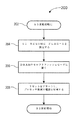
図2は、本開示の少なくとも1つの実施形態に係る、S3スリープ状態へサスペンドする処理システムを準備する方法200を示す図である。説明の簡潔を期するため、方法200は、図1に示す処理システム100の例示のコンテキストで説明する。最後のユーザ入力または他のスリープモード状態からの比較的長い静止に応じて、ブロック202において、OS120は、例えば、処理システム100をS3スリープ状態に置く割込みハンドラを呼び出すシステム管理割込み(SMI)などの割込みを信号で伝える。または、OS120は、ダイレクトOS(direct OS)または高位ソフトウェア命令によって、S3スリープ状態へのサスペンドを信号で伝える。
FIG. 2 is a diagram illustrating a
プロセッサ装置126は、フラグS3_RESUME_FLAGを用いて、リセットからの復帰が、S3休止状態からのレジュームによるものであるのか、または、パワーオンリセットによるものであるのかを示す。したがって、ブロック204で、割込みハンドラまたはレジュームコントローラ116は、処理システム100がS3状態にある間、引き続き電力が供給されている1つ以上のフロップまたは他の記憶素子に特定の値(例えば、「1」)を記憶させることによって、フラグS3_RESUME_FLAGをアサートする。一実施形態では、フラグS3_RESUME_FLAGは、最初にサウスブリッジ112のNVRAM124(S3スリープ状態の間、電力が供給されている)に記憶され、その後、レジュームコントローラ116は、S3スリープ状態からのレジュームプロセスの一部として、このフラグのコピーを、ノースブリッジ108の制御レジスタ119に移動させる。
The processor device 126 uses the flag S3_RESUME_FLAG to indicate whether the return from the reset is due to the resume from the S3 hibernation state or the power-on reset. Accordingly, at
ブロック206で、割込みハンドラまたはレジュームコントローラ116は、処理システム100がS3状態の間ではDRAM102に記憶された情報を維持するように、DRAM102をセルフリフレッシュモードに置く。ブロック208で、電力管理コントローラ118は、リセット信号をアサートする。リセット信号がアサートされている期間、プロセッサ装置126は、パワーダウン(電源が切断)される。本明細書で使用される「パワーダウン(電源が切断)」という用語は、レジスタ、キャッシュ、フロップ、他の記憶素子の状態が確実に保持されていない状態に置かれることを指す。これは、プロセッサ装置の構成要素の一部または全部に非動作電圧を提供する(すなわち、記憶素子の保持電圧よりも低い電圧を提供する)こと、プロセッサ装置の構成要素の一部または全部をクロックゲートすることなどによって、プロセッサ装置126の構成要素の一部または全部から電力を完全に遮断することで達成し得る。この時点では、処理システム100は、S3スリープ状態にあると考えられる。
At
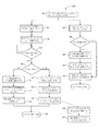
図3は、本開示の少なくとも1つの実施形態に係る、パワーオンリセットおよびS3スリープ状態からのレジュームの何れかからプロセッサ装置126を初期化する方法の一例300を示す図である。方法300は、ブロック302から開始され、プロセッサ装置126のリセット信号がデアサート(deassert)される。リセット信号のデアサートは、パワーオンリセットによってコールドブートを信号で伝えること、または、S3スリープ状態から動作状態へのレジュームを指示する信号を伝えることによって生じ得る。後者の場合には、例えば、処理システム100がS3スリープ状態にある間に、ユーザの電源ボタンまたはユーザ入力装置の操作に応じてタイマを終了させることによって、信号が伝えられる。プロセッサ装置126は、フラグWAIT_BOOT_INITを用いて、プロセッサコア106がブートコードを実行するのを予備初期化が実行されるまで停止させる。このフラグは、ブロック302でWAIT_BOOT_INITを1に設定することによって、停止状態に初期化されてもよい。
FIG. 3 is a diagram illustrating an
ブロック304で、リセットのデアサートは、レジュームコントローラ116に伝達され、ブロック306でフラグS3_RESUME_FLAGの状態をチェックすることによって、レジュームプロセスを開始する。レジュームコントローラ116が、S3_RESUME_FLAGがアサートされた(例えば、1に等しい)と判定し、これにより、リセットのデアサートがS3状態からのレジュームの結果であると示す場合には、ブロック308で、レジュームコントローラ116は、DRAM102をセルフリフレッシュモードから終了させる。その後、レジュームコントローラ116は、S3スリープ状態中にMC状態イメージ138が記憶されていたフラッシュメモリ104またはNVRAM124からMC状態イメージ138にアクセスし、MC状態イメージ138に表されるコンテキスト情報を用いて、メモリコントローラ114の以前の状態を構成又は他の方法で復元する。この構成は、メモリコントローラ114に関するタイミング情報の復元と、以前のアドレスマッピング情報の復元(例えば、ページテーブルの構成)等を含んでもよい。
At
プロセッサ装置126は、フラグS3_EXIT_RSTを用いて、リセットからの復帰がS3状態からのレジュームであるか否かをBSPに信号で伝える。メモリコントローラ114の構成後に、レジュームコントローラ116は、ブロック310でフラグS3_EXIT_RSTをアサートする。上述したように、プロセッサ装置126は、フラグWAIT_BOOT_INITを用いて、プロセッサコア106がブートコードを実行するのを、予備初期化が実行されるまで停止させる。したがって、メモリコントローラ114の復元と、フラグS3_EXIT_RSTのアサートとの後に、ブロック312で、レジュームコントローラ116は、フラグWAIT_BOOT_INITをデアサートすることによって、BSPおよびその他のプロセッサコア106を解放して、後述するような実行を開始させる。フラグS3_EXIT_RSTおよびWAIT_BOOT_INITは、例えばノースブリッジ108の1つ以上の制御レジスタ119に配置され得る。
The processor device 126 uses the flag S3_EXIT_RST to signal to the BSP whether or not the return from the reset is resume from the S3 state. After configuration of the
ブロック306に戻り、レジュームコントローラ116が、S3_RESUME_FLAGがアサートされていないと判定することによって、パワーオンリセット、または、S3スリープ状態以外の状態からの復帰であると示す場合には、フラグS3_EXIT_RSTはアサートされないままであり(例えば、「0」)、方法300のフローは、ブロック306からブロック312にジャンプして、後述するようにフラグWAIT_BOOT_INITがデアサートされる。
Returning to block 306, the flag S3_EXIT_RST is not asserted if the
ブロック304〜312のプロセスと並行して、ブロック302でのリセットのデアサートが、ブロック314でBSPおよび他のプロセッサコア106に伝達される。それに応じて、ブロック316で、BSPは、リセットマイクロコードの実行を開始して、例えば、パワーオン自己テスト(POST)を実行すること、コア組込み自己診断テスト(BIST)を実行すること、コアのヒューズを分配すること、初期化シーケンスの残りに備えるのに必要な内部コンテキストを初期化することによって、プロセッサ装置126を予備的に初期化する。予備初期化の完了後に、ブロック318で、プロセッサコア106は、フラグがデアサートされるまで制御レジスタ119に繰り返しフラグWAIT_BOOT_INITをポーリングすることによって、プロセッサコア106を解放して実行を開始させる。プロセッサコア106は、解放されると、ブロック320でフラグS3_EXIT_RSTにアクセスして、ブロック302でのリセットのデアサートがパワーオンリセットによるものなのか(S3_EXIT_RST=0)、または、S3スリープ状態からのレジュームによるものなのか(S3_EXIT_RST=1)を判定する。
In parallel with the process of blocks 304-312, the reset deassertion at
フラグS3_EXIT_RSTがデアサートされる場合(例えば、「0」)には、方法300のフローは、フラッシュメモリ104を用いて実行されるBIOS初期化プロセスに向かう。したがって、ブロック322で、BSPは、リセットマイクロコードの実行を完了し、これにより、プロセッサ装置126の予備初期化を完了する。これに応じて、ブロック324で、BSPの命令ポインタは、コールドブートBIOS初期化に用いられるデフォルトリセットベクトルに設定され、ブロック326で、BSPは、フラッシュメモリ104からのリセットBIOSイメージ130のリセットブートコード128の実行を開始して、システム初期化プロセスを完了する。一実施形態では、リセットブートコード128は、レジュームBIOSイメージ132のコピーをDRAM102に記憶するようにBSPを操作する命令を含み、これにより、リセットブートコード128の実行は、ブロック328でのフラッシュメモリ104からDRAM102へのレジュームBIOSイメージ132のコピーの転送と、ブロック329でのフラッシュメモリ104からNVRAM124へのMC状態イメージ138のコピーの転送と、を含んでもよい。リセットブートコード128の実行が完了すると、1つ以上のプロセッサコア106のIPがOS120の最初のベクトルに設定され、ブロック330で処理システム100の制御がOS120に転送されることによって、処理システム100の初期化が完了する。
If the flag S3_EXIT_RST is deasserted (eg, “0”), the flow of the
ブロック320に戻り、フラグS3_EXIT_RSTがアサートされる場合(例えば、「1」)には、方法300のフローは、フラッシュメモリ104ではなくDRAM102に記憶されるレジュームブート構成情報を用いて実行されるBIOS再初期化工程に向かう。したがって、ブロック332で、プロセッサコア106の一部または全部は、マイクロコードまたは他のファームウェアを実行して、復元されたメモリコントローラ114を介して、DRAM102から対応するコア状態イメージ134にアクセスする。次に、各プロセッサコア106は、対応するコア状態イメージ134に記憶されるコンテキスト情報に基づいて、コンテキストをロードする。各コア状態イメージ134は、レジュームBIOSイメージ132のレジュームブートコード136の対応するレジュームベクトルを含み、ブロック334で、このレジュームベクトルは、対応するプロセッサコア106の命令ポインタにロードされる。ブロック336で、プロセッサコア106は、DRAM102から個々のレジュームベクトルで始まるレジュームブートコード136の実行を開始して、処理システム100の初期化を完了させる。レジュームブートコード136の実行が完了すると、1つのプロセッサコア106のIPがOS120の最初のベクトルに設定され、ブロック330で処理システム120の制御がOS120に転送されることによって、処理システム100の再初期化が完了する。
Returning to block 320, if the flag S3_EXIT_RST is asserted (eg, “1”), the flow of the
少なくとも1つの実施形態では、上記の装置および技術が、図1に示すプロセッサ装置126などの1つ以上の集積回路(IC)デバイス(集積回路パッケージまたはマイクロチップと称される)を備えるシステムにおいて実現される。電子設計自動化(EDA)とコンピュータ支援設計(CAD)ソフトウェアツールを、これらのICデバイスの設計と製造に使用することができる。通常、これらの設計ツールは、1つ以上のソフトウェアプログラムによって表される。1つ以上のソフトウェアプログラムは、プロセスの少なくとも一部を実行して、回路を製造する製造システムを設計または改造するように、コンピュータシステムによって実行可能なコードを含み、1つ以上のICデバイスの回路を表すコードに基づき動作するようにコンピュータシステムを操作する。このコードは、命令、データ、または、命令およびデータの組み合わせを含んでもよい。設計ツールまたは製造ツールを表すソフトウェア命令は、通常、コンピューティングシステムにアクセス可能なコンピュータ可読記憶媒体に記憶されている。同様に、ICデバイスの設計または製造の1つ以上の段階を表すコードは、同一のコンピュータ可読記憶媒体または異なるコンピュータ可読記憶媒体に記憶され得るし、これらの媒体からアクセスされ得る。 In at least one embodiment, the apparatus and techniques described above are implemented in a system comprising one or more integrated circuit (IC) devices (referred to as integrated circuit packages or microchips) such as the processor unit 126 shown in FIG. Is done. Electronic design automation (EDA) and computer aided design (CAD) software tools can be used to design and manufacture these IC devices. These design tools are typically represented by one or more software programs. The one or more software programs include code executable by the computer system to perform at least a portion of the process to design or modify a manufacturing system that manufactures the circuit. The computer system is operated to operate based on the code representing The code may include instructions, data, or a combination of instructions and data. Software instructions representing design tools or manufacturing tools are typically stored on a computer readable storage medium accessible to the computing system. Similarly, code representing one or more stages of IC device design or manufacture may be stored on or accessed from the same computer-readable storage medium or different computer-readable storage media.
コンピュータ可読記憶媒体は、使用中にコンピュータシステムによってアクセス可能であり、命令および/もしくはデータをコンピュータシステムに送る任意の記憶媒体または記憶媒体の組み合わせを含んでもよい。このような記憶媒体は、光学媒体(例えば、コンパクトディスク(CD)、デジタル多用途ディスク(DVD)、ブルーレイ(登録商標)ディスク)、磁気媒体(例えば、フロッピー(登録商標)ディスク、磁気テープまたは磁気ハードドライブ)、揮発性メモリ(例えば、ランダムアクセスメモリ(RAM)またはキャッシュ)、不揮発性メモリ(例えば、読出し専用メモリ(ROM)またはフラッシュメモリ)、または、微小電気機械システム(MEMS)ベースの記憶媒体を含んでもよいが、これらに限定されない。コンピュータ可読記憶媒体は、コンピューティングシステムに埋め込まれてもよく(例えば、システムRAMまたはROM)、コンピューティングシステムに固着されてもよく(例えば、磁気ハードドライブ)、コンピューティングシステムに脱着可能に装着されてもよく(例えば、光ディスクまたはユニバーサルシリアルバス(USB)ベースのフラッシュメモリ)、有線または無線ネットワークを介してコンピュータシステムに接続されてもよい(例えば、ネットワークアクセス可能ストレージ(NAS))。 A computer-readable storage medium may be any storage medium or combination of storage media that is accessible by a computer system during use and that sends instructions and / or data to the computer system. Such storage media can be optical media (eg, compact disc (CD), digital versatile disc (DVD), Blu-ray® disc), magnetic media (eg, floppy disc, magnetic tape or magnetic). Hard drive), volatile memory (eg, random access memory (RAM) or cache), non-volatile memory (eg, read only memory (ROM) or flash memory), or micro-electromechanical system (MEMS) based storage media However, it is not limited to these. The computer readable storage medium may be embedded in the computing system (eg, system RAM or ROM), secured to the computing system (eg, magnetic hard drive), and removably attached to the computing system. It may be (eg, an optical disc or Universal Serial Bus (USB) based flash memory) and may be connected to a computer system via a wired or wireless network (eg, network accessible storage (NAS)).
図4は、本開示の少なくとも1つの実施形態に係る本発明の1つ以上の態様を実現する、ICデバイスを設計および製造する方法の例400を示すフローチャートである。上述したように、以下の各プロセスで生成されるコードは、対応する設計ツールもしくは製造ツールによるアクセスと使用のためにコンピュータ可読記憶媒体に記憶され、または、他の方法で具体化される。
FIG. 4 is a flowchart illustrating an
ブロック402で、ICデバイスの機能仕様が生成される。機能仕様(マイクロアーキテクチャ仕様(MAS)と称されることも多い)は、C、C++、システムC、シミュリンク、もしくは、MATLABなどの様々なプログラミング言語またはモデリング言語によって表すことができる。
At
ブロック404で、機能仕様が用いられ、ICデバイスのハードウェアを表すハードウェア記述コードが生成される。少なくとも1つの実施形態では、ハードウェア記述コードは、ICデバイスの回路の形式記述と設計のために、様々なコンピュータ言語、仕様言語またはモデリング言語を含む少なくとも1つのハードウェア記述言語(HDL)によって表される。通常、生成されたHDLコードは、ICデバイスの回路の動作、回路の設計と構造、シミュレーションを通じてICデバイスの正常動作を検証する試験を表す。HDLの例は、アナログHDL(AHDL)、ベリログHDL、システムベリログHDL、VHDLなどである。同期デジタル回路を実現するICデバイスの場合には、ハードウェア記述コードは、同期デジタル回路の動作の抽象的表示を提供するレジスタ転送レベル(RTL)コードを含んでもよい。他の種類の回路の場合には、ハードウェア記述コードは、回路の動作の抽象的表示を提供する挙動レベルコードを含んでもよい。通常、ハードウェア記述コードによって表されるHDLモデルは、設計検証をパスするために、1回以上の回数のシミュレーションとデバッギングとを受ける。
At
ハードウェア記述コードによって表される設計の検証後に、ブロック406で、合成ツールを用いてハードウェア記述コードを合成し、ICデバイスの回路の最初の物理的実装を表示または定義するコードを生成する。一実施形態では、合成ツールは、回路素子要素(例えば、ゲート、トランジスタ、レジスタ、コンデンサ、インダクタ、ダイオードなど)と、回路素子要素間のネットまたは接続と、を含む1つ以上のネットリストを生成する。または、ネットリストの全部または一部は、合成ツールを用いずに手動で生成することができる。ハードウェア記述コードと同様に、ネットリストも、最後のセットの1つ以上のネットリストが生成される前に、1つ以上の試験および検証プロセスを受けることができる。
After verification of the design represented by the hardware description code, at
または、概要エディタツールを用いてICデバイスの回路概要をドラフトした後に、概要捕捉ツールを使用して、結果としてできる回路図を捕捉し、構成要素と回路の接続を表す1つ以上のネットリスト(コンピュータ可読媒体に記憶されている)を生成することができる。その後、取得された回路図は、試験と検証のために、1つ以上の回数のシミュレーションを受けることができる。 Alternatively, after drafting a circuit overview of an IC device using the overview editor tool, the overview capture tool can be used to capture the resulting schematic and include one or more netlists that represent the connections between components and circuits ( Stored on a computer readable medium). The acquired circuit diagram can then be subjected to one or more simulations for testing and verification.
ブロック408で、1つ以上のEDAツールは、ブロック406で製造されたネットリストを用いて、ICデバイスの回路の物理レイアウトを表すコードを生成する。このプロセスは、例えば、ICデバイスの回路の各要素の位置を決定または固定するためのネットリストを用いる配置ツールを含んでもよい。さらに、ルーティングツールは、配置プロセスに基づき、ネットリストにしたがって回路素子を接続するのに必要な配線を追加し、経路を決定する。結果として生じるコードは、ICデバイスの3次元モデルを表す。コードは、例えばグラフィックデータベースシステムII(GDSII)フォーマットなどのデータベースファイルフォーマットで表され得る。このフォーマットのデータは、通常、階層構造の回路レイアウトに関する幾何的形状、テキストラベルおよび他の情報を表す。
At
ブロック410で、物理レイアウトコード(例えば、GDSIIコード)は、物理レイアウトコードを用いる製造設備に提供され、製造設備の製造ツール(例えば、マスクワークを通じて)を構成または他の方法で改造して、ICデバイスを製造する。すなわち、物理レイアウトコードは、1つ以上のコンピュータシステムに組み込まれた後に、製造設備のツールの作業、または、そこで実行される製造作業の一部または全部を制御することができる。
At
なお、概略的な説明で上述した行為または要素の全てが必須というわけではなく、特定の工程または装置の一部については不要であってもよく、上述のものに加えて、1つ以上の他の工程を実行してもよいし、1つ以上の他の要素を含んでもよい。さらに、工程の順番は、必ずしも上記の工程が実行された順番とは限らない。 Note that not all of the acts or elements described above in the general description are required, and some of the particular steps or devices may be unnecessary, and in addition to those described above, one or more other These steps may be performed and may include one or more other elements. Furthermore, the order of the steps is not necessarily the order in which the above steps are performed.
また、コンセプトを具体的な実施形態を参照して説明した、しかし、当業者であれば、以下の請求項に記載される本開示の範囲を逸脱することなく様々な修正や変更を加えることができると理解するであろう。したがって、明細書及び図面は、限定的ではなく例示的であるとみなすべきであり、上記の全ての修正は、本開示の範囲に属するものと意図される。 The concepts have been described with reference to specific embodiments, but those skilled in the art can make various modifications and changes without departing from the scope of the present disclosure as set forth in the claims below. You will understand that you can. The specification and drawings are accordingly to be regarded as illustrative rather than restrictive, and all such modifications are intended to be within the scope of the disclosure.
具体的な実施形態を参照して、利益、他の利点、課題の解決策を説明した。しかしながら、利益と、利点と、課題の解決策と、任意の利益、利点、課題の解決策を生じさせ又は明確にすることのできる特徴とは、請求項の一部又は全部にとって極めて重要であり、必要であり又は必須であると解釈すべきではない。 Benefits, other advantages, and solutions to problems have been described with reference to specific embodiments. However, benefits, benefits, solutions to problems, and features that can generate or clarify any benefits, advantages, solutions to problems are critical to some or all of the claims. Should not be construed as necessary or essential.
Claims (10)
前記プロセッサ装置の初期化に続いて前記プロセッサ装置を低電力状態に置くことと、
前記プロセッサ装置がパワーダウンされている前記低電力状態からレジュームするという指示に応じて、前記低電力状態の間に前記揮発性メモリに記憶された第2のブート構成情報のコピーを用いて、前記プロセッサ装置を再初期化することと、を含み、
前記プロセッサ装置を再初期化することは、
前記第2のブート構成情報のコア状態情報に基づいて、前記プロセッサ装置のプロセッサコアのコンテキストを構成することであって、前記プロセッサコアの命令ポインタを、前記第2のブート構成情報の第2のブートコードのリセットベクトルに設定することを含む、ことと、
前記プロセッサコアを用いて前記第2のブートコードを実行することと、を含む方法。 In response to a power-on reset of the processor device, the processor device is initialized using the first boot configuration information stored in the nonvolatile memory, and the boot code of the first boot configuration information is executed And transferring a copy of the second boot configuration information from the non-volatile memory to the volatile memory;
Placing the processor device in a low power state following initialization of the processor device;
Wherein the processor unit is powered down in response to the instruction to resume from a low power state, using said copy of the second boot configuration information stored in said volatile memory during the low power state, the anda reinitializing the processor device,
Re-initializing the processor device includes
Based on the core status information of the second boot configuration information, the method comprising: configuring the context of a processor core of the processor unit, the instruction pointer of the processor core, the second of the second boot configuration information Including setting the boot code reset vector, and
Executing the second boot code using the processor core.
前記不揮発性メモリに記憶されたメモリコントローラ構成情報を用いて、前記プロセッサ装置のメモリコントローラを構成することと、
前記構成されたメモリコントローラを介して前記揮発性メモリから前記第2のブート構成情報にアクセスすることと、
を含む請求項1の方法。 Re-initializing the processor device includes
Using the memory controller configuration information stored in the non-volatile memory to configure the memory controller of the processor device;
Accessing the second boot configuration information from the volatile memory via the configured memory controller;
The method of claim 1 comprising:
前記プロセッサ装置がパワーダウンされている低電力状態からレジュームするという指示に応じて、
前記プロセッサ装置のメモリコントローラを構成することと、
前記プロセッサ装置が、前記メモリコントローラを用いて、前記揮発性メモリから構成情報にアクセスすることと、
前記低電力状態の間に、前記構成情報を用いて、前記プロセッサ装置のプロセッサコアの命令ポインタを、前記揮発性メモリに保持された前記第2のブートコードのリセットベクトルに設定することと、
前記プロセッサ装置にて、前記メモリコントローラによって前記揮発性メモリからアクセスされた前記第2のブートコードを実行することと、を含む方法。 In response to a power-on reset of the processor device, the processor device executes the first boot code accessed from the nonvolatile memory, and transfers the second boot code from the nonvolatile memory to the volatile memory. When,
In response to an instruction to resume from a low power state in which the processor device is powered down,
Configuring a memory controller of the processor device;
And said processor unit, using the memory controller to access the configuration information from the volatile memory,
Setting the instruction pointer of the processor core of the processor device to the reset vector of the second boot code held in the volatile memory using the configuration information during the low power state;
Executing at the processor device the second boot code accessed from the volatile memory by the memory controller.
前記メモリコントローラを構成することは、前記不揮発性メモリから前記メモリコントローラ構成情報にアクセスすることと、前記メモリコントローラ構成情報を用いて前記メモリコントローラを構成することと、を含む請求項6の方法。 In said nonvolatile memory, storing the memory controller configuration information further includes a,
7. The method of claim 6 , wherein configuring the memory controller includes accessing the memory controller configuration information from the non-volatile memory and configuring the memory controller using the memory controller configuration information.
前記プロセッサ装置は、
揮発性メモリに接続可能なメモリコントローラと、
前記メモリコントローラに接続されたリセットコントローラであって、前記プロセッサ装置がパワーダウンされている低電力状態からレジュームするという指示に応じて、前記メモリコントローラを構成するリセットコントローラと、
前記メモリコントローラに接続されたプロセッサコアであって、前記プロセッサ装置のパワーオンリセットに応じて、不揮発性メモリに記憶された第1のブート構成情報を用いて前記プロセッサ装置を初期化し、前記低電力状態からレジュームするという指示に応じて、前記メモリコントローラを介して前記揮発性メモリからアクセスされる第2のブート構成情報を用いて、前記プロセッサ装置を再初期化するプロセッサコアと、を備え、
前記プロセッサコアは、前記第1のブート構成情報のブートコードを実行して、第2のブート構成情報のコピーを前記不揮発性メモリから前記揮発性メモリに転送することによって、前記プロセッサ装置を初期化し、
前記第2のブート構成情報はブートコードを含み、
前記プロセッサコアは、前記プロセッサコアの命令ポインタを前記第2のブート構成情報の前記ブートコードのリセットベクトルに設定し、前記プロセッサコアを用いて前記第2のブート構成情報の前記ブートコードを実行することによって、前記プロセッサ装置を再初期化する、
システム。 A system comprising a processor device,
The processor device includes:
A memory controller connectable to volatile memory;
A reset controller connected to the memory controller, the reset controller configuring the memory controller in response to an instruction to resume from a low power state in which the processor device is powered down;
A processor core connected to the memory controller, wherein the processor device is initialized using first boot configuration information stored in a non-volatile memory in response to a power-on reset of the processor device; A processor core that re-initializes the processor device using second boot configuration information accessed from the volatile memory via the memory controller in response to an instruction to resume from a state;
The processor core initializes the processor device by executing a boot code of the first boot configuration information and transferring a copy of the second boot configuration information from the nonvolatile memory to the volatile memory. ,
The second boot configuration information includes a boot code;
Said processor core sets the instruction pointer of the processor core reset vector of the boot code of the second boot configuration information, executes the boot code of the second boot configuration information using the processor core Reinitializing the processor device,
system.
Applications Claiming Priority (5)
| Application Number | Priority Date | Filing Date | Title |
|---|---|---|---|
| IN1637DE2012 | 2012-05-30 | ||
| IN1637/DEL/2012 | 2012-05-30 | ||
| US13/547,701 US9182999B2 (en) | 2012-05-30 | 2012-07-12 | Reintialization of a processing system from volatile memory upon resuming from a low-power state |
| US13/547,701 | 2012-07-12 | ||
| PCT/US2013/043057 WO2013181220A1 (en) | 2012-05-30 | 2013-05-29 | Reinitalization of a processing system from volatile memory upon resuming from a low-power state |
Publications (3)
| Publication Number | Publication Date |
|---|---|
| JP2015523645A JP2015523645A (en) | 2015-08-13 |
| JP2015523645A5 JP2015523645A5 (en) | 2016-07-14 |
| JP6126211B2 true JP6126211B2 (en) | 2017-05-10 |
Family
ID=49671782
Family Applications (1)
| Application Number | Title | Priority Date | Filing Date |
|---|---|---|---|
| JP2015515142A Active JP6126211B2 (en) | 2012-05-30 | 2013-05-29 | Reinitialization of processing system from volatile memory when resuming from low power state |
Country Status (6)
| Country | Link |
|---|---|
| US (1) | US9182999B2 (en) |
| EP (1) | EP2856308A1 (en) |
| JP (1) | JP6126211B2 (en) |
| KR (1) | KR101959002B1 (en) |
| CN (1) | CN104412224B (en) |
| WO (1) | WO2013181220A1 (en) |
Families Citing this family (37)
| Publication number | Priority date | Publication date | Assignee | Title |
|---|---|---|---|---|
| TWI510903B (en) * | 2012-11-19 | 2015-12-01 | Wistron Corp | Computer system and data recovery method thereof |
| US9594567B2 (en) * | 2013-02-21 | 2017-03-14 | Dell Products, Lp | Configuring a trusted platform module |
| JP6478562B2 (en) | 2013-11-07 | 2019-03-06 | 株式会社半導体エネルギー研究所 | Semiconductor device |
| US10079019B2 (en) | 2013-11-12 | 2018-09-18 | Apple Inc. | Always-on audio control for mobile device |
| US10587471B1 (en) * | 2013-12-17 | 2020-03-10 | Amazon Technologies, Inc. | Criterion-based computing instance activation |
| CN105960633B (en) * | 2014-02-07 | 2020-06-19 | 株式会社半导体能源研究所 | Semiconductor device, device and electronic apparatus |
| US9778728B2 (en) | 2014-05-29 | 2017-10-03 | Apple Inc. | System on a chip with fast wake from sleep |
| US10031000B2 (en) | 2014-05-29 | 2018-07-24 | Apple Inc. | System on a chip with always-on processor |
| US9619377B2 (en) | 2014-05-29 | 2017-04-11 | Apple Inc. | System on a chip with always-on processor which reconfigures SOC and supports memory-only communication mode |
| US20150362980A1 (en) * | 2014-06-16 | 2015-12-17 | Apple Inc. | Always-On Processor as a Coprocessor |
| US9785447B2 (en) * | 2014-06-27 | 2017-10-10 | Intel Corporation | System standby emulation with fast resume |
| US10055370B2 (en) * | 2014-07-09 | 2018-08-21 | Advanced Micro Devices, Inc. | Method and apparatis for processor standby |
| US9479331B2 (en) * | 2014-08-20 | 2016-10-25 | Apple Inc. | Managing security in a system on a chip (SOC) that powers down a secure processor |
| JP6180450B2 (en) * | 2015-02-02 | 2017-08-16 | キヤノン株式会社 | Control device, control method and program for control device |
| US10037071B2 (en) * | 2015-02-25 | 2018-07-31 | Texas Instruments Incorporated | Compute through power loss approach for processing device having nonvolatile logic memory |
| US10452594B2 (en) | 2015-10-20 | 2019-10-22 | Texas Instruments Incorporated | Nonvolatile logic memory for computing module reconfiguration |
| CN105487865A (en) * | 2015-11-27 | 2016-04-13 | 山东超越数控电子有限公司 | Method for solving problem of abnormal arousal of system by USB device |
| US10331203B2 (en) | 2015-12-29 | 2019-06-25 | Texas Instruments Incorporated | Compute through power loss hardware approach for processing device having nonvolatile logic memory |
| CN107015847A (en) * | 2016-01-28 | 2017-08-04 | 扬智科技股份有限公司 | Electronic installation and its Working mode switching method |
| TWI615705B (en) * | 2016-05-31 | 2018-02-21 | 瑞昱半導體股份有限公司 | Method for resetting a memory in a computer system |
| JP6723863B2 (en) * | 2016-08-01 | 2020-07-15 | オリンパス株式会社 | Embedded system, photography equipment and refresh method |
| US10990159B2 (en) * | 2017-04-25 | 2021-04-27 | Apple Inc. | Architected state retention for a frequent operating state switching processor |
| US20190004818A1 (en) * | 2017-06-29 | 2019-01-03 | American Megatrends Inc. | Method of UEFI Shell for Supporting Power Saving Mode and Computer System thereof |
| US10783252B2 (en) * | 2017-08-23 | 2020-09-22 | Qualcomm Incorporated | System and method for booting within a heterogeneous memory environment |
| KR102406571B1 (en) * | 2017-12-28 | 2022-06-08 | 삼성전자주식회사 | Image display apparatus and operating method for the same |
| US10643672B2 (en) * | 2018-03-23 | 2020-05-05 | Micron Technology, Inc. | Memory with non-volatile configurations for efficient power management and operation of the same |
| US11550592B2 (en) * | 2018-06-29 | 2023-01-10 | Intel Corporation | Methods and apparatus to utilize non-volatile memory for computer system boot |
| CN110727244B (en) * | 2019-03-18 | 2021-03-26 | 北京中鼎高科自动化技术有限公司 | Multi-axis motion control system and method with memory starting mode |
| US11042213B2 (en) * | 2019-03-30 | 2021-06-22 | Intel Corporation | Autonomous core perimeter for low power processor states |
| FR3094830A1 (en) * | 2019-04-08 | 2020-10-09 | Proton World International N.V. | Power supply circuit for volatile memory |
| US11112983B2 (en) * | 2019-08-28 | 2021-09-07 | Micron Technology, Inc. | Recovery of memory device from a reduced power state |
| US11513970B2 (en) * | 2019-11-01 | 2022-11-29 | International Business Machines Corporation | Split virtual memory address loading mechanism |
| US11494248B2 (en) * | 2019-12-20 | 2022-11-08 | Qualcomm Incorporated | Warm mission-mode reset in a portable computing device |
| US10877541B1 (en) * | 2019-12-30 | 2020-12-29 | Micron Technology, Inc. | Power delivery timing for memory |
| US20230176735A1 (en) * | 2020-05-22 | 2023-06-08 | Intel Corporation | Accelerating system boot times via host-managed device memory |
| US20230061037A1 (en) * | 2021-09-01 | 2023-03-02 | Micron Technology, Inc. | Apparatus with power-based data protection mechanism and methods for operating the same |
| CN115061558B (en) * | 2022-06-16 | 2023-08-15 | 飞腾信息技术有限公司 | Hot reset method and device of PCIE equipment, storage medium and PCIE equipment |
Family Cites Families (13)
| Publication number | Priority date | Publication date | Assignee | Title |
|---|---|---|---|---|
| US5448521A (en) * | 1993-11-12 | 1995-09-05 | International Business Machines Corporation | Connecting a short word length non-volatile memory to a long word length address/data multiplexed bus |
| JPH11161385A (en) * | 1997-11-28 | 1999-06-18 | Toshiba Corp | Computer system and its system state control method |
| US6571333B1 (en) | 1999-11-05 | 2003-05-27 | Intel Corporation | Initializing a memory controller by executing software in second memory to wakeup a system |
| DE10393639D2 (en) * | 2002-08-30 | 2005-07-14 | Philips Semiconductors Dresden | Method for initialization of programmable systems |
| US20040117318A1 (en) * | 2002-12-16 | 2004-06-17 | Grawrock David W. | Portable token controlling trusted environment launch |
| CN100415085C (en) * | 2004-08-13 | 2008-09-03 | 中国海洋大学 | Method of cutturing polyploid seed breedign using diploid/tetraploid oclimera abalone |
| EP1653331B8 (en) | 2004-10-29 | 2012-03-14 | ST-Ericsson SA | An apparatus and method for entering and exiting low power mode |
| US7797523B2 (en) | 2006-09-25 | 2010-09-14 | Hewlett-Packard Development Company, L.P. | Method and system of executing stack-based memory reference code |
| US20090204837A1 (en) * | 2008-02-11 | 2009-08-13 | Udaykumar Raval | Power control system and method |
| US20090292934A1 (en) * | 2008-05-22 | 2009-11-26 | Ati Technologies Ulc | Integrated circuit with secondary-memory controller for providing a sleep state for reduced power consumption and method therefor |
| KR101602360B1 (en) * | 2009-07-14 | 2016-03-10 | 엘지전자 주식회사 | System fast booting apparatus and method |
| KR20110100466A (en) * | 2010-03-04 | 2011-09-14 | 삼성전자주식회사 | Powerdown method for system having volatile memory devices |
| WO2013015924A1 (en) * | 2011-07-26 | 2013-01-31 | Marvell World Trade Ltd. | Zero power hibernation mode with instant on |
-
2012
- 2012-07-12 US US13/547,701 patent/US9182999B2/en active Active
-
2013
- 2013-05-29 WO PCT/US2013/043057 patent/WO2013181220A1/en active Application Filing
- 2013-05-29 CN CN201380028476.XA patent/CN104412224B/en active Active
- 2013-05-29 JP JP2015515142A patent/JP6126211B2/en active Active
- 2013-05-29 EP EP13729163.9A patent/EP2856308A1/en not_active Ceased
- 2013-05-29 KR KR1020147035472A patent/KR101959002B1/en active IP Right Grant
Also Published As
| Publication number | Publication date |
|---|---|
| US9182999B2 (en) | 2015-11-10 |
| JP2015523645A (en) | 2015-08-13 |
| KR101959002B1 (en) | 2019-07-02 |
| WO2013181220A8 (en) | 2014-10-16 |
| EP2856308A1 (en) | 2015-04-08 |
| CN104412224A (en) | 2015-03-11 |
| WO2013181220A9 (en) | 2014-12-11 |
| US20130326206A1 (en) | 2013-12-05 |
| KR20150016331A (en) | 2015-02-11 |
| WO2013181220A1 (en) | 2013-12-05 |
| CN104412224B (en) | 2018-01-09 |
Similar Documents
| Publication | Publication Date | Title |
|---|---|---|
| JP6126211B2 (en) | Reinitialization of processing system from volatile memory when resuming from low power state | |
| US8910177B2 (en) | Dynamic mapping of logical cores | |
| US8438416B2 (en) | Function based dynamic power control | |
| US9262322B2 (en) | Method and apparatus for storing a processor architectural state in cache memory | |
| US20160077575A1 (en) | Interface to expose interrupt times to hardware | |
| US9395919B1 (en) | Memory configuration operations for a computing device | |
| TW445416B (en) | Upgrade card for a computer system and method of operating the same | |
| US9298243B2 (en) | Selection of an operating point of a memory physical layer interface and a memory controller based on memory bandwidth utilization | |
| TW201430572A (en) | Assigning processors to memory mapped configuration | |
| US20040117743A1 (en) | Heterogeneous multi-processor reference design | |
| CN112753069B (en) | Dynamic configuration of memory timing parameters | |
| CN110573991B (en) | Architecture state reservation | |
| US20190004818A1 (en) | Method of UEFI Shell for Supporting Power Saving Mode and Computer System thereof | |
| US20160180487A1 (en) | Load balancing at a graphics processing unit | |
| US9378027B2 (en) | Field-programmable module for interface bridging and input/output expansion | |
| WO2020106482A1 (en) | Programming and controlling compute units in an integrated circuit | |
| CN108984464B (en) | Microprocessor and method for synchronizing processing cores of microprocessor | |
| US20140136819A1 (en) | Register file management for operations using a single physical register for both source and result | |
| US20150193259A1 (en) | Boosting the operating point of a processing device for new user activities | |
| US8997210B1 (en) | Leveraging a peripheral device to execute a machine instruction | |
| CN110046126B (en) | Multi-core microprocessor, reconfiguration method thereof, and computer-readable storage medium | |
| CN112912958A (en) | Testing read-only memory using built-in self-test controller | |
| JP6196315B2 (en) | Store regeneration policy | |
| TWI599959B (en) | Electronic apparatus for supporting different firmware functions and operation method thereof | |
| JP2007087176A (en) | Storage element verification method for logic circuit |
Legal Events
| Date | Code | Title | Description |
|---|---|---|---|
| A521 | Request for written amendment filed |
Free format text: JAPANESE INTERMEDIATE CODE: A523 Effective date: 20160524 |
|
| A621 | Written request for application examination |
Free format text: JAPANESE INTERMEDIATE CODE: A621 Effective date: 20160524 |
|
| A871 | Explanation of circumstances concerning accelerated examination |
Free format text: JAPANESE INTERMEDIATE CODE: A871 Effective date: 20160524 |
|
| A975 | Report on accelerated examination |
Free format text: JAPANESE INTERMEDIATE CODE: A971005 Effective date: 20160620 |
|
| A131 | Notification of reasons for refusal |
Free format text: JAPANESE INTERMEDIATE CODE: A131 Effective date: 20160628 |
|
| A521 | Request for written amendment filed |
Free format text: JAPANESE INTERMEDIATE CODE: A523 Effective date: 20160927 |
|
| A131 | Notification of reasons for refusal |
Free format text: JAPANESE INTERMEDIATE CODE: A131 Effective date: 20161101 |
|
| TRDD | Decision of grant or rejection written | ||
| A01 | Written decision to grant a patent or to grant a registration (utility model) |
Free format text: JAPANESE INTERMEDIATE CODE: A01 Effective date: 20170314 |
|
| A61 | First payment of annual fees (during grant procedure) |
Free format text: JAPANESE INTERMEDIATE CODE: A61 Effective date: 20170406 |
|
| R150 | Certificate of patent or registration of utility model |
Ref document number: 6126211 Country of ref document: JP Free format text: JAPANESE INTERMEDIATE CODE: R150 |
|
| R250 | Receipt of annual fees |
Free format text: JAPANESE INTERMEDIATE CODE: R250 |
|
| R250 | Receipt of annual fees |
Free format text: JAPANESE INTERMEDIATE CODE: R250 |
|
| R250 | Receipt of annual fees |
Free format text: JAPANESE INTERMEDIATE CODE: R250 |
|
| R250 | Receipt of annual fees |
Free format text: JAPANESE INTERMEDIATE CODE: R250 |
|
| R250 | Receipt of annual fees |
Free format text: JAPANESE INTERMEDIATE CODE: R250 |