以下、図面を参照して本発明の好適な実施形態について詳細に説明する。なお、本発明は以下の実施形態に限定されるものではなく、本発明の実施に有利な具体例を示すにすぎない。また、以下の実施形態の中で説明されている特徴の組み合わせの全てが本発明の課題解決のために必須のものであるとは限らない。
(第1の実施形態)
図1は、本発明の実施形態に係る撮像装置500の構成の一例を示すブロック図である。撮像装置500は、二つの処理回路100(第1の処理回路)と処理回路200(第2の処理回路)を備えている。本実施形態では、これら二つの処理回路100、200はそれぞれが一つの集積回路(IC)として構成される。
また、二つの処理回路100と処理回路200の間で通信を行うためのデータバス300が設けられている。処理回路100、200はそれぞれ独立に撮像部400から動画データを取得することが可能である。処理回路100、200はそれぞれ、撮像部400から取得した動画データを処理することが可能である。
次に、処理回路100と処理回路200の構成について説明する。処理回路100は、画像処理部101、CPU102(Central Processing Unit)(第1のCPU)、メモリ103、記録再生部104、コーデック部105、通信部106、バス107を有する。本実施形態では、メモリ103としてSDRAMを使用する。また、メモリ103は処理回路100に内蔵されているが、処理回路100の外部に設けられてもよい。
CPU102は、メモリ103に格納されているコンピュータプログラム(ソフトウェア)に従って、撮像装置500全体の動作を制御する。メモリ103は、CPU102のワークエリアとして機能する。なお、CPU102のワークエリアは、メモリ103に限られるものではなく、ハードディスクドライブ等の外部記録装置等であってもよい。画像処理部101は、撮像部400から取得した静止画データに対して画素補間処理や色変換処理等の画像処理を行う。画像処理部101は、撮像部400から取得したRGB色空間の動画データをYUV色空間のデータフォーマットに変換する。また、画像処理部101は、撮像部400が取得した画像の画素数(画面サイズ)を縮小、或いは拡大(リサイズ)する。
撮像部400及び画像処理部101は、CPU102によって、オートフォーカス(AF)処理及び自動露出制御(AE)処理を行うように制御される。CPU102から撮影を行うように指示された場合、撮像部400及び画像処理部101は露光処理や現像処理等の処理を含む撮影処理を実行する。撮像部400は、CCDやCMOS等の撮像素子やAD変換器等を備える。撮像部400は、撮像素子により得られたアナログ信号をデジタルデータに変換して出力する。撮像部400から取得された静止画データは、YUV形式の静止画データとしてメモリ103に記憶される。メモリ103に記憶された静止画データに対して、コーデック部105(第1の符号化部、第1の復号部)により符号化処理が行われ、静止画データのデータ量が圧縮される。
記録再生部104は、記録時においては、符号化された静止画データを記録媒体211に書き込む。コーデック部105は、撮影時においては、撮像部400より取得した静止画データをJPEG等の公知の符号化方式により符号化する。
通信部106(第1の通信部)は、処理回路200との間で動画データやその他必要なコマンドを送受信する。通信部106は、動画データを受信するためのデータ受信部106a、画像データを送信するためのデータ送信部106b、制御コマンドなどのメッセージを送るためのメッセージ通信部106cを有する。通信部106での通信はデータバス300を介して行われる。それぞれの通信は独立して行うことが可能である。
本実施形態においては、後述のように、連写後、処理回路100により処理されたインデクス用の画像データが通信部106により処理回路200に送信される。
処理回路200は、画像処理部201、CPU202(第2のCPU)、メモリ203、記録再生部204、コーデック部205、通信部206、ファイル制御部207、表示部208、操作部209、バス210を有する。本実施形態では、メモリ203としてSDRAMを使用する。また、メモリ203は処理回路100に内蔵されているが、処理回路200の外部にメモリ203を設けることも可能である。画像処理部201、CPU202、メモリ203、コーデック部205、通信部206(第2の通信部)の各ブロックは処理回路100における各ブロックと同様の機能を持つ。
処理回路200は、撮影時には、撮像部400から動画データを取得して、コーデック部205(第2の符号化部、第2の復号部)により符号化処理を行う。記録再生部204は、記録時においては、コーデック部205により符号化された静止画データを記録媒体212に記録する。記録媒体211は、メモリカードなどのランダムアクセス媒体である。また、本実施形態では、不図示の装着、排出機構により、容易に装着、排出が可能となっている。また、記録媒体211を撮像装置500に内蔵する構成としてもよい。CPU202は、操作部209により指定された画素数や画質の設定に従って静止画データの記録を制御する。また、記録再生部204は、再生時においては、後述のようにユーザによって選択された静止画データを記録媒体211から読み出す。コーデック部205は、再生時においては、記録媒体211から読み出された静止画データを復号する。
画像処理部201(第2のリサイズ部)は、撮影時においては、撮像部400から取得した動画データの画像サイズを表示部208のサイズに合わせて変更してメモリ203に記憶する。そして、リサイズされたデータが表示部208に供給されて表示される。また、再生時においては、画像処理部201は、再生された静止画データのサイズを表示部208のサイズに合わせて変更してメモリ203に記憶する。そして、リサイズされたデータが表示部208に供給されて表示される。表示部208は、撮影された画像や再生された画像の他、各種の必要な情報を表示する。CPU202は、表示部208に表示する情報を生成して表示部208に送る。
ファイル制御部207は、所定のファイルシステムに従い、記録媒体211に記録された静止画をファイルとして管理する。本実施形態では、FATファイルシステムに従い、記録媒体211に記録された画像ファイルを管理する。なお、本実施形態では、ファイル制御部207は処理回路200に設けている。ファイル制御部207は、電源投入時、或いは、記録媒体が装着された場合に、記録媒体211からファイルシステムに係る管理情報(FATやディレクトリエントリなど)を読み出し、メモリ203に記憶する。そして、記録媒体211に対する記録処理に伴い、メモリ203に記憶された管理情報を変更(更新)する。そして、静止画記録時などの所定のタイミングで、メモリ203より管理情報を読み出し、記録再生部204により記録媒体211に記録することにより、記録媒体212の管理情報を更新する。
操作部209は、撮像装置500を操作するためのユーザインターフェースとして機能する。操作部209は、撮像装置500を操作するための電源ボタン、モード変更ボタン、シャッターボタン、十字ボタン、メニューボタン等を有し、各ボタンはスイッチ、タッチパネル等により構成される。CPU202は、操作部209を介して入力されたユーザの指示に従って撮像装置500を制御する。ユーザによって操作部209のボタンが操作された場合、操作部209から各ボタンに応じた操作信号がCPU202に入力される。CPU202は操作部209から入力された操作信号を解析し、解析結果に応じて操作信号に対応した処理を判定する。CPU202は、操作部209から入力された操作信号に対応した処理を実行するように撮像装置500の各部を制御する。
ユーザは操作部209を操作することにより、撮影する画像の露光時間(シャッタ速度)や記録する画像のサイズ(画素数)と画質(圧縮率)などを設定することができる。また、ユーザは、操作部209を操作することにより、撮影された画像に対し、ノイズ低減処理などの特殊な処理を施すか否かを設定することができる。CPU202は、ユーザによるこれらの設定に基づいて、撮像部400により撮影される画像データの露光時間や、撮影された画像に対する処理を制御する。また、CPU202は、操作部209のシャッターボタンがユーザにより連続して操作されている場合に、所定のタイミングで連続的に撮影指示を発行することにより、静止画の連写を行う。また、CPU202は、撮影される画像データの露光時間、撮影された画像に対する処理、画像データを一時記憶するメモリ203の空き容量や記録再生部204によるデータの書き込み速度などにより、連写中に発行する撮影指示の間隔を変更することができる。
次に、撮像装置500における記録時の処理について説明する。図2は処理回路200における記録時の処理を示すフローチャートである。図2の処理はCPU202が各部を制御することにより実行される。まず、記録に先立ち、ファイル制御部207は、記録媒体211から読み出した管理情報(FAT)に基づいて、記録媒体211における空き領域を判別する。ファイル制御部207は、この空き領域に基づいて、記録媒体211に対してデータを書き込むための書き込みアドレスを決める。
操作部209より静止画撮影の指示があった場合、CPU202は、通信部206により通信を行うことにより、処理回路100が撮影待機状態、即ち、撮像部400により撮影された静止画を処理しているか否かを判別する(S201)。処理回路100が待機状態である場合、CPU202は、通信部206により、処理回路100に対し撮影指示を出力する(S212)。処理回路100が待機状態ではない場合、CPU202は、撮像部400から1フレームの静止画データを取得し、画像処理部201にてYUV色空間データに変換した後、メモリ203に記憶する(S202)。次に、CPU202は、コーデック部205により、メモリ203に記憶された静止画データを符号化し、メモリ203に記憶する。ここでメモリ203に記憶された静止画データは、インデクス画像として使用するため、電源がオフされるか、或いは、メモリ203の空き領域が無くなって削除されるまで、メモリ203に保持される。
1画面の静止画データの処理が完了した場合、CPU202は、ファイル制御部207に対し、この符号化データの書き込みを指示する。ファイル制御部207は、記録媒体212の空き領域から書き込みアドレスを決定し、記録再生部204に対しデータの書き込みを指示する。記録再生部204はメモリ203より符号化データを読み出し、記録媒体211の指定されたアドレスに書き込む(S203)。データの書き込みが完了した場合、ファイル制御部207は、メモリ203に記憶された管理情報の内容を更新すると共に、空き領域も更新する。
次に、CPU202は、処理回路100から、符号化された静止画データのデータ量の情報が通知されたか否かを判別する(S204)。データ量の情報が通知された場合、CPU202は、記録再生部204により記録媒体211に直前に書き込まれた静止画データの書き込みアドレスと、通知されたデータ量とに基づいて、処理回路100による符号化データの書き込みアドレスを決定する。そして、決定した書き込みアドレスをデータ送信部206aより処理回路100に送信する(S205)。即ち、CPU202は、連写時において、直前に書き込まれた静止画データの最終書き込みアドレスを含むクラスタの次のクラスタの先頭から処理回路100が符号化データを書き込むように、書き込みアドレスを決定する。
このように書き込みアドレスの情報を送信した後、CPU202は、処理回路100から符号化データの書き込み完了の通知が送信されたか否かを判別する(S206)。書き込み完了の通知がデータ受信部206bにより受信された場合、CPU202は、ファイル制御部207に対し、FATを更新するように指示する。ファイル制御部207は、処理回路100による書き込みに応じて、メモリ203に記憶されたFATの内容を更新する(S207)。
次に、CPU202は、後述のように、データ受信部206bが処理回路100からのインデクス画像を受信したか否かを判別する(S208)。ここで、データ受信部206bがインデクス画像データを受信した場合、これをメモリ203に記憶する(S209)。このとき、メモリ203におけるインデクス画像データのための記憶領域に空きが無い場合、CPU202は、メモリ203から最も古い画像データを削除することができる。こうしてメモリ203の空き領域が確保され、受信した画像データがメモリ203に記憶される。
次に、CPU202は、操作部209により撮影指示の操作が行われているか否かを判別する(S210)。撮影指示の操作が行われている場合、CPU202は、S201に戻って処理を続ける。また、撮影指示の操作が行われていない場合、CPU202は、メモリ203に記憶された管理情報を記録媒体211に書き込むように記録再生部204に指示する。記録再生部204は、メモリ203から管理情報を読み出し、記録媒体211に記録する(S211)。
図3は、処理回路100における記録時の処理を示すフローチャートである。図3の処理はCPU102が各部を制御することにより実行される。CPU102は、通信部106により、処理回路200から撮影指示(図2のS212参照。)を受けたか否かを判別する(S301)。撮影指示を受けていない場合はS307に進む。撮影指示を受けた場合、CPU102は、撮像部400から1フレームの画像データを取得し、画像処理部101にてYUV色空間データに変換した後、メモリ103に記憶する(S302)。ここでメモリ103に記憶された静止画データは、静止画の記録終了後に、インデクス画像として処理回路100に転送される。そのため、電源がオフされるか、メモリ103の空き領域が無くなって削除されるまで、或いは、処理回路200への転送が完了するまで、メモリ103に保持される。次に、CPU102は、符号化された静止画データのサイズの情報をメッセージ通信部106cにより処理回路200に送信する(S304)。
次に、CPU102は、処理回路200から、記録媒体211における書き込みアドレスの情報(図2のS205参照。)が受信されたか否かを判別する(S305)。書き込みアドレスの情報が受信されていた場合、CPU102は、記録媒体211における指定された書き込みアドレスに、メモリ103に記憶された静止画データを書き込むように記録再生部104に指示する。記録再生部104は、メモリ103より符号化された静止画データを読み出し、記録媒体211の指定された書き込みアドレスに書き込む(S306)。符号化データの書き込みが完了すると、CPU102は、メッセージ通信部106cにより、書き込み完了の通知を処理回路200に送信する(S307)。次に、CPU102は、メモリ103よりインデクス用の画像データを読み出し、データ送信部106bより処理回路200に送信する(S308)。(図2のS208参照。)
このように、処理回路100による画像データの記録が終了した後、インデクス画像のための画像データが処理回路100から処理回路200に送信され、メモリ203に記憶される。
次に、再生時におけるインデクス画面の生成処理を説明する。操作部209よりインデクス表示の指示があった場合、CPU202は、インデクス画面を生成する。本実施形態では、インデクス画面の表示の指示があった場合、撮影の順に、最新の画像からn画面分のサムネイル画像を生成し、これらn画面のサムネイル画像を含むインデクス画面が表示される。なお、1画面に表示するサムネイル画像の画面数nを、ユーザが操作部209を操作することにより決める構成としてもよい。この場合、CPU102は、設定されている画面数nに基づいて、表示すべきサムネイル画像を決める。
図4は処理回路200によるインデクス画面の表示処理を示すフローチャートである。図4の処理はCPU202が各部を制御することにより実行される。まず、CPU202は、前述のように決定したサムネイル画像の一つを指定する(S401)。そして、CPU202は、指定された画像データがメモリ203に記憶されているか否かを判別する(S402)。メモリ203に指定された画像データが記憶されていた場合、CPU202は、コーデック部205により指定された画像データを復号する(S403)。CPU202は、画像処理部201により復号された画像データのサイズを縮小し、メモリ203のインデクス画面用の記憶領域に記憶する(S404)。次に、CPU202は、表示すべき全てのサムネイル画像がメモリ203に記憶され、表示準備が完了したか否かを判別する(S405)。全てのサムネイル画像がメモリ203に記憶され、表示準備が完了した場合、CPU202は、各サムネイル画像データをメモリ103より読み出し、インデクス画面を生成して表示部208に表示する(S406)。
S402において、メモリ203に指定された画像データが記憶されていない場合、CPU202は、記録再生部204により、指定された画像データを記録媒体211から読み出す(S407)。そして、読み出した画像データをコーデック部205により復号する。
このようにインデクス画面が表示部208に表示された後、ユーザが操作部209を操作して再生する画像を指定し、再生を指示することができる。再生が指示された場合、CPU202は、記録再生部204により、指定された画像データを記録媒体211より読み出し、コーデック部205によりデコードする。そして、デコードされた静止画データを画像処理部201により縮小し、表示部208により表示する。
このように、本実施形態では、二つの処理回路100、200により静止画を撮影し記録する構成において、処理回路100による1画面の画像データの記録終了後、画像データを処理回路200に転送する。そして、転送された画像データを処理回路200におけるメモリ203に記憶しておく。そのため、インデクス画面の表示の指示があった場合、このメモリ203に記憶された画像データからサムネイル画像を生成し、インデクス画面を表示することにより、迅速にインデクス画面を表示することができる。また、1画面の静止画の記録が完了する度に、処理回路100に画像データが転送され、メモリ203に記憶される。そのため、連写後のインデクス表示があった場合にも迅速にインデクス画面を表示することができる。
なお、本実施形態では、処理回路100により記録される画像データをインデクス用の画像データとして処理回路200に送信したが、処理回路100によりサムネイル画像のサイズに縮小した状態で処理回路200に送信する構成としてもよい。こうすることで、処理回路200への画像データの送信に要する時間が短くなり、CPU202の処理負荷が軽減され、また、バス210の占有時間も短くなる。更に、メモリ203に対して記憶できるインデクス画像の数も増やすことができる。
(第2の実施形態)
次に、第2の実施形態を説明する。本実施形態においても、撮像装置の構成は図1の構成と同様である。第1の実施形態では、処理回路100は、1画面の画像データの記録処理が終了した後に、インデクス画像データを処理回路200に送信していた。これに対し第2の実施形態では、処理回路200のCPU202が、処理回路100に対しインデクス画像データの送信を指示し、処理回路100はこの送信指示に応答してインデクス画像データを処理回路200に送信する。そして、CPU202は、処理回路200における連写速度に基づいて、連写速度が遅く、CPU202の能力やバス210の処理帯域に余裕がある状態であるか否かを判定する。そして、この判定結果により、CPU202が、処理回路100に対してインデクス画像データの送信を指示する。
図5は、本実施形態における処理回路200による記録処理を示すフローチャートである。第1の実施形態に係る図2における処理ステップと同一の処理ステップには同一の参照番号を付しその説明を省略する。図5においては、S201とS202の間に、S502,S503,S504の処理ステップが介在する。S201において処理回路100が待機状態でない場合、CPU202は、処理回路200における連写速度が低く、処理回路100からのインデクス画像データを受信する状態であるか否かを判断する(S502)。インデクス画像データを受信すると判断した場合、CPU202は、メッセージ通信部206cにより、処理回路100に対してインデクス画像データの送信を指示する(S503)。一方、インデクス画像データを受信しないと判断した場合、CPU202は、処理回路100に対してインデクス画像データの送信停止を指示する(S504)。処理回路100では、メッセージ通信部106cがインデクス画像の送信指示、或いは、送信停止指示を受信すると、受信した指示をメモリ103に記憶する。
次に、S502における判定処理について説明する。CPU202は、操作部209からの撮影指示が出力されていない状態と、連写中の処理回路200の状態とに基づいて、連写速度が低い状態であるか否かを判別する。そして、連写速度が低く、処理回路200によるCPU202の処理に余裕があり、また、バス210の処理帯域に余裕があると判断した場合に、処理回路100からのインデクス画像を受信すると判断する。
図7は、撮影指示が出力されていない状態においてCPU202によって実行される連写速度の判定処理を示すフローチャートである。図7の処理は、撮影待機状態において、CPU202により繰り返し実行される。CPU202は、ユーザにより設定されたシャッタ速度に基づく露光時間が閾値よりも長いか否かを判別する(S701)。露光時間が閾値よりも長い場合、CPU202は、連写速度が低いと判定する(S702)。また、S701で露光時間が閾値以下であった場合、CPU202は、ノイズ低減処理など、処理に時間がかかる所定の長時間処理がユーザにより設定されているか否かを判別する(S703)。長時間処理が設定されていた場合、CPU202は、連写速度が低いと判定する(S704)。また、長時間処理が設定されていない場合、CPU202は、ユーザにより設定された画像のサイズや画質に基づき、処理される画像のデータ量が多いか否かを判別する(S705)。処理データ量が多い設定、例えば、複数種類のサイズのうち、画像のサイズが最も大きいものに設定され、かつ、複数種類の画質のうち、最も高い画質であり、圧縮後のデータ量が多い場合、CPU202は、連写速度が低いと判定する(S706)。このように、連写速度が低いと判定した場合、CPU202は、判定結果をメモリ203に記憶しておく。
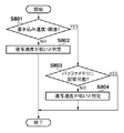
図8は、撮影(連写)開始後においてCPU202により実行される判断処理を示すフローチャートである。図8の処理は、撮影処理の実行中、CPU202により繰り返し実行される。CPU202は、記録媒体211に対するデータの書き込み可能速度が閾値よりも高いか否かを判別する(S801)。データの書き込み速度が閾値よりも高くない場合、連写速度が低いと判定する(S802)。また、データの書き込み速度が閾値よりも高い場合、CPU202は、メモリ203における、記録する画像データを一時記憶するためのバッファメモリ領域に空きがあり、データの記憶が可能であるか否かを判別する(S803)。バッファメモリ領域に空きがなくなると、CPU202は、撮像部400から画像データを取得する間隔を長くするように変更する。そのため、CPU202は、バッファメモリ領域に空きが無い場合は連写速度が低いと判断する(S804)。このように、連写速度が低いと判定した場合、CPU202は、判定結果をメモリ203に記憶する。
S502においては、CPU202は、図7、図8の処理によってメモリ203に記憶された判定結果に基づいて連写速度が低いと判定した場合に、インデクス画像を受信すると判断する。
図6は、第2の実施形態における処理回路100の記録時の処理を示すフローチャートである。第1の実施形態に係る図3における処理ステップと同一の処理ステップには同一の参照番号を付しその説明を省略する。図6において、CPU102は、S307で処理回路200に対して書き込み完了を通知した後、インデクス画像の送信指示を処理回路200から受信したか否かを判別する(S608)。インデクス画像の送信指示を受信していた場合、CPU102は、メモリ103に記憶された未送信の画像データのうち最も新しい画像データをデータ送信部106bより処理回路200に送信する(S308)。ここでは、CPU102は、1画面の画像データを送信する度に、処理回路200からの指示を確認し、処理回路200からインデクス画像の送信停止指示を受けるまでは、未送信の画像データの送信を続ける。そして、未送信の画像データを全て送信した場合、CPU102は、処理回路200への画像データの送信を停止する。
一方、未送信の画像データがメモリ103に記憶されている場合であっても、処理回路200よりインデクス画像の送信停止指示が発行された場合、CPU102は、処理回路200に画像データを送信せず、メモリ103に保持する。また、メモリ103の空き領域がなく、新たに生成されたインデクス画像データを記憶することができない場合、CPU102は、送信済みの画像データを削除して、新たに生成された画像データをメモリ103に記憶する。
次に、再生時におけるインデクス画面の生成処理を説明する。図9は処理回路200によるインデクス画面の表示処理を示すフローチャートである。図9の処理はCPU202が各部を制御することにより実行される。第1の実施形態に係る図4における処理ステップと同一の処理ステップには同一の参照番号を付しその説明を省略する。S402において、メモリ203に指定された画像データが記憶されていない場合、CPU202は、メッセージ通信部206cにより、指定された画像データが処理回路100のメモリ103に記憶されているかを処理回路100に問い合わせる(S907)。この結果、処理回路100より、指定された画像データがメモリ103に記憶されている旨の応答をメッセージ通信部206cにより受信した場合、CPU202は、指定した画像データの転送を処理回路100に指示する(S908)。そして、CPU202は、データ受信部206bにより画像データを受信し(S909)、指定された画像データをコーデック部205によりデコードする(S403)。このように、CPU202は、表示指示に係る画像データがメモリ203に記憶されていない場合、処理回路100のメモリ103に対して当該表示指示に係る画像データの取得を試行する。
また、S907で、メモリ103に指定された画像データが記憶されていない旨の応答を受信した場合、CPU202は、記録再生部204により、指定された画像データを記録媒体211から読み出す(S407)。こうして、CPU202は、S907〜S909の試行による上記表示指示に係る画像データの取得に失敗した場合には、当該表示指示に係る画像データを記録媒体211から取得することができる。そして、読み出した画像データをコーデック部205により復号する(S403)。
このようにインデクス画面が表示部208に表示された後、ユーザが操作部209を操作して再生する画像を指定し、再生を指示することができる。再生が指示された場合、CPU202は、記録再生部204により、指定された画像データを記録媒体211より読み出し、コーデック部205によりデコードする。そして、デコードされた静止画データを画像処理部201により縮小し、表示部208により表示する。
このように、第2の実施形態では、CPU202は、処理回路200の処理負荷に応じて、処理回路100に対して画像データの送信指示又は送信停止指示を発行する。処理負荷は例えば連写速度で判定することができる。処理回路200による連写速度が低く、処理回路200が処理回路100により生成されたインデクス用の画像データを受信して記憶できる場合に、処理回路100から処理回路200に画像データが送信される。そのため、連写中に処理回路100から処理回路200に対して画像データを送信することでCPU202の負荷が大きくなり、更に、バス210の処理帯域が圧迫されることにより、撮影処理が中断することが無い。
(他の実施形態)
また、本発明は、以下の処理を実行することによっても実現される。即ち、上述した実施形態の機能を実現するソフトウェア(プログラム)を、ネットワーク又は各種記憶媒体を介してシステム又は装置に供給し、そのシステム又は装置のコンピュータ(またはCPUやMPU等)がプログラムを読み出して実行する処理である。この場合、そのプログラム、及び該プログラムを記憶した記憶媒体は本発明を構成することになる。