JP6087630B2 - Wiring board with customized layer - Google Patents
Wiring board with customized layer Download PDFInfo
- Publication number
- JP6087630B2 JP6087630B2 JP2012557087A JP2012557087A JP6087630B2 JP 6087630 B2 JP6087630 B2 JP 6087630B2 JP 2012557087 A JP2012557087 A JP 2012557087A JP 2012557087 A JP2012557087 A JP 2012557087A JP 6087630 B2 JP6087630 B2 JP 6087630B2
- Authority
- JP
- Japan
- Prior art keywords
- layer
- trace
- insulating material
- traces
- wiring board
- Prior art date
- Legal status (The legal status is an assumption and is not a legal conclusion. Google has not performed a legal analysis and makes no representation as to the accuracy of the status listed.)
- Expired - Fee Related
Links
Images


Classifications
-
- H—ELECTRICITY
- H05—ELECTRIC TECHNIQUES NOT OTHERWISE PROVIDED FOR
- H05K—PRINTED CIRCUITS; CASINGS OR CONSTRUCTIONAL DETAILS OF ELECTRIC APPARATUS; MANUFACTURE OF ASSEMBLAGES OF ELECTRICAL COMPONENTS
- H05K3/00—Apparatus or processes for manufacturing printed circuits
- H05K3/46—Manufacturing multilayer circuits
- H05K3/4644—Manufacturing multilayer circuits by building the multilayer layer by layer, i.e. build-up multilayer circuits
- H05K3/4647—Manufacturing multilayer circuits by building the multilayer layer by layer, i.e. build-up multilayer circuits by applying an insulating layer around previously made via studs
-
- H—ELECTRICITY
- H05—ELECTRIC TECHNIQUES NOT OTHERWISE PROVIDED FOR
- H05K—PRINTED CIRCUITS; CASINGS OR CONSTRUCTIONAL DETAILS OF ELECTRIC APPARATUS; MANUFACTURE OF ASSEMBLAGES OF ELECTRICAL COMPONENTS
- H05K3/00—Apparatus or processes for manufacturing printed circuits
- H05K3/10—Apparatus or processes for manufacturing printed circuits in which conductive material is applied to the insulating support in such a manner as to form the desired conductive pattern
- H05K3/12—Apparatus or processes for manufacturing printed circuits in which conductive material is applied to the insulating support in such a manner as to form the desired conductive pattern using thick film techniques, e.g. printing techniques to apply the conductive material or similar techniques for applying conductive paste or ink patterns
- H05K3/1241—Apparatus or processes for manufacturing printed circuits in which conductive material is applied to the insulating support in such a manner as to form the desired conductive pattern using thick film techniques, e.g. printing techniques to apply the conductive material or similar techniques for applying conductive paste or ink patterns by ink-jet printing or drawing by dispensing
-
- H—ELECTRICITY
- H05—ELECTRIC TECHNIQUES NOT OTHERWISE PROVIDED FOR
- H05K—PRINTED CIRCUITS; CASINGS OR CONSTRUCTIONAL DETAILS OF ELECTRIC APPARATUS; MANUFACTURE OF ASSEMBLAGES OF ELECTRICAL COMPONENTS
- H05K3/00—Apparatus or processes for manufacturing printed circuits
- H05K3/46—Manufacturing multilayer circuits
- H05K3/4644—Manufacturing multilayer circuits by building the multilayer layer by layer, i.e. build-up multilayer circuits
- H05K3/4664—Adding a circuit layer by thick film methods, e.g. printing techniques or by other techniques for making conductive patterns by using pastes, inks or powders
-
- H—ELECTRICITY
- H05—ELECTRIC TECHNIQUES NOT OTHERWISE PROVIDED FOR
- H05K—PRINTED CIRCUITS; CASINGS OR CONSTRUCTIONAL DETAILS OF ELECTRIC APPARATUS; MANUFACTURE OF ASSEMBLAGES OF ELECTRICAL COMPONENTS
- H05K2203/00—Indexing scheme relating to apparatus or processes for manufacturing printed circuits covered by H05K3/00
- H05K2203/04—Soldering or other types of metallurgic bonding
- H05K2203/049—Wire bonding
-
- H—ELECTRICITY
- H05—ELECTRIC TECHNIQUES NOT OTHERWISE PROVIDED FOR
- H05K—PRINTED CIRCUITS; CASINGS OR CONSTRUCTIONAL DETAILS OF ELECTRIC APPARATUS; MANUFACTURE OF ASSEMBLAGES OF ELECTRICAL COMPONENTS
- H05K3/00—Apparatus or processes for manufacturing printed circuits
- H05K3/40—Forming printed elements for providing electric connections to or between printed circuits
- H05K3/4007—Surface contacts, e.g. bumps
- H05K3/4015—Surface contacts, e.g. bumps using auxiliary conductive elements, e.g. pieces of metal foil, metallic spheres
-
- H—ELECTRICITY
- H05—ELECTRIC TECHNIQUES NOT OTHERWISE PROVIDED FOR
- H05K—PRINTED CIRCUITS; CASINGS OR CONSTRUCTIONAL DETAILS OF ELECTRIC APPARATUS; MANUFACTURE OF ASSEMBLAGES OF ELECTRICAL COMPONENTS
- H05K3/00—Apparatus or processes for manufacturing printed circuits
- H05K3/40—Forming printed elements for providing electric connections to or between printed circuits
- H05K3/4038—Through-connections; Vertical interconnect access [VIA] connections
- H05K3/4046—Through-connections; Vertical interconnect access [VIA] connections using auxiliary conductive elements, e.g. metallic spheres, eyelets, pieces of wire
-
- Y—GENERAL TAGGING OF NEW TECHNOLOGICAL DEVELOPMENTS; GENERAL TAGGING OF CROSS-SECTIONAL TECHNOLOGIES SPANNING OVER SEVERAL SECTIONS OF THE IPC; TECHNICAL SUBJECTS COVERED BY FORMER USPC CROSS-REFERENCE ART COLLECTIONS [XRACs] AND DIGESTS
- Y10—TECHNICAL SUBJECTS COVERED BY FORMER USPC
- Y10T—TECHNICAL SUBJECTS COVERED BY FORMER US CLASSIFICATION
- Y10T29/00—Metal working
- Y10T29/49—Method of mechanical manufacture
- Y10T29/49002—Electrical device making
- Y10T29/49117—Conductor or circuit manufacturing
- Y10T29/49124—On flat or curved insulated base, e.g., printed circuit, etc.
- Y10T29/49155—Manufacturing circuit on or in base
- Y10T29/49165—Manufacturing circuit on or in base by forming conductive walled aperture in base
Description
(原文の対応する箇所に記載なし) (There is no description in the corresponding part of the original text)
[0001] いくつかの既知の配線基板は、当該配線基板の外面において特定のパターンに配置された電気素子への電気的接続を与える。このような配線基板の一例としては、プローブヘッドであり、プローブヘッドは、プローブヘッドの外面上に特定のパターンに配置された導電性プローブと、プローブへの内部配線とを有しうる。本発明の実施形態は、標準ベース配線基板にカスタマイズ層を追加するプロセスを含む。カスタマイズ層は、カスタマイズ層の外面における、プローブのようなカスタム配置された電気素子へのカスタマイズされた電気的接続を与える。このようなプロセスは、所望のパターンに配置されていない接点を有するベース配線基板が、ベース配線基板上の接点のパターンとは異なる所望のパターンに配置されたプローブといった電気素子を有するようにカスタマイズされることを可能にしうる。 [0001] Some known wiring boards provide an electrical connection to electrical elements arranged in a specific pattern on the outer surface of the wiring board. An example of such a wiring board is a probe head, and the probe head may have a conductive probe arranged in a specific pattern on the outer surface of the probe head and an internal wiring to the probe. Embodiments of the present invention include a process for adding a customization layer to a standard base wiring board. The customization layer provides a customized electrical connection to a custom placed electrical element, such as a probe, on the outer surface of the customization layer. Such a process is customized so that a base wiring board having contacts that are not arranged in a desired pattern has electrical elements such as probes arranged in a desired pattern different from the pattern of contacts on the base wiring board. Can make it possible.
[0002] 本発明のいくつかの実施形態では、ベース基板を得ることによって多層配線基板内に電気ジャンパを作成しうる。ベース基板は、当該ベース基板の表面上にカスタマイズ層を含みうる。カスタマイズ層は、第1電気絶縁材料層の外面上に導電性トレース層を含みうる。トレース層は、第1トレース、第2トレース及び第3トレースを含みうる。第3トレースの一部は、第1トレース及び第2トレースの端間の空間内にありうる。プロセスは、第1トレース及び第2トレースの端間の空間内、及び、第3トレースの一部上に、電気絶縁物質をプリントすることも含み、また、プロセスは、第3トレースに電気的に接触することなく第1トレース及び第2トレースに電気的に接続する電気ジャンパを形成することをさらに含みうる。電気ジャンパは、第1トレースの端、絶縁物質及び第2トレースの端上に導電性物質をプリントすることによって形成されうる。 [0002] In some embodiments of the present invention, an electrical jumper may be created in a multilayer wiring board by obtaining a base substrate. The base substrate may include a customization layer on the surface of the base substrate. The customization layer can include a conductive trace layer on the outer surface of the first electrically insulating material layer. The trace layer can include a first trace, a second trace, and a third trace. A portion of the third trace can be in the space between the ends of the first trace and the second trace. The process also includes printing an electrically insulating material in the space between the ends of the first and second traces and on a portion of the third trace, and the process is electrically connected to the third trace. It may further include forming an electrical jumper that is electrically connected to the first trace and the second trace without contact. The electrical jumper may be formed by printing a conductive material on the end of the first trace, the insulating material, and the end of the second trace.
[0003] 本発明のいくつかの実施形態では、多層配線基板は、ベース基板と、ベース基板の表面上のカスタマイズ層とを含みうる。カスタマイズ層は、第1電気絶縁材料層と、第1絶縁材料層の表面上の第1導電性トレース層とを含みうる。第1トレース層は、第1トレース、第2トレース及び第3トレースを含み、第3トレースの一部は、第1トレース及び第2トレースの端間の空間内にありうる。カスタマイズ層はさらに、第3トレースの一部上と、第1トレース及び第2トレースの端間の空間内に、乾燥プリント可能導電材料を含む電気絶縁物質を含みうる。カスタマイズ層はさらに、導電性ジャンパを含み、導電性ジャンパは、第1トレース及び第2トレースの端上の乾燥プリント可能導電材料と、絶縁物質とを含む導電性物質を含みうる。ジャンパは、第3トレースに電気的に接触することなく第1トレース及び第2トレースを電気的に接続しうる。 [0003] In some embodiments of the present invention, the multilayer wiring board may include a base substrate and a customization layer on the surface of the base substrate. The customization layer can include a first electrically insulating material layer and a first conductive trace layer on a surface of the first insulating material layer. The first trace layer includes a first trace, a second trace, and a third trace, and a portion of the third trace may be in a space between the ends of the first trace and the second trace. The customization layer may further include an electrically insulating material including a dry printable conductive material on a portion of the third trace and in the space between the ends of the first and second traces. The customization layer further includes a conductive jumper, and the conductive jumper may include a conductive material including a dry printable conductive material on the ends of the first and second traces and an insulating material. The jumper can electrically connect the first trace and the second trace without electrically contacting the third trace.
[0004] 本発明のいくつかの実施形態では、多層配線基板は、ベース基板の表面上の第1導電性トレース層内の導電性トレースに結合されかつそこから延在する導電性の第1ビア構造を形成することを含むプロセスによって作成されうる。プロセスはさらに、ベース基板の表面に結合され、第1ビア構造がその中に埋め込まれる剛性の第1電気絶縁材料層を形成することを含みうる。剛性の第1電気絶縁材料層は、第1ビア構造の周りにかつ第1トレース層及びベース基板の表面上に第1電気絶縁材料層を流し込む(casting)ことによって形成されうる。第1ビア構造は、第1トレース層内のトレースから第1絶縁材料層の外面への電気的接続を与えうる。 [0004] In some embodiments of the present invention, the multilayer wiring board includes a first conductive via coupled to and extending from a conductive trace in a first conductive trace layer on the surface of the base substrate. It can be created by a process that includes forming a structure. The process may further include forming a rigid first electrically insulating material layer coupled to the surface of the base substrate and having the first via structure embedded therein. A rigid first electrically insulating material layer may be formed by casting the first electrically insulating material layer around the first via structure and on the first trace layer and the surface of the base substrate. The first via structure may provide an electrical connection from the trace in the first trace layer to the outer surface of the first insulating material layer.
[0005] 本発明のいくつかの実施形態では、多層配線基板は、ベース基板と、ベース基板の表面上の第1導電性トレース層とを含みうる。配線基板はさらに、第1トレース層上にかつベース基板の表面上に結合された剛性の第1電気絶縁材料層を含み、配線基板はまたさらに、第1絶縁材料層内に埋め込まれた導電性の複数の第1ビアを含みうる。第1ビアの各々は、第1トレース層のトレースのうちの1つに接合し、第1絶縁材料層の外面へと延在するワイヤスタッドのスタック又はワイヤを含みうる。 [0005] In some embodiments of the present invention, the multilayer wiring board may include a base substrate and a first conductive trace layer on a surface of the base substrate. The wiring board further includes a rigid first electrically insulating material layer coupled on the first trace layer and on the surface of the base substrate, the wiring board also further comprising a conductive material embedded in the first insulating material layer. A plurality of first vias. Each of the first vias may include a stack or wire of wire studs that joins one of the traces of the first trace layer and extends to the outer surface of the first insulating material layer.
[0006] 本発明のいくつかの実施形態では、多層配線基板における電気的接続は、複数のカスタマイズ層をその表面上に含むベース基板を得ることを含むプロセスによって作成されうる。カスタマイズ層は、第1導電性トレース層における第1トレースと、第1導電性トレース層を覆う第1電気絶縁材料層と、第1絶縁材料層の外面上の第2導電性トレース層における第2トレースとを含みうる。プロセスはさらに、第1電気絶縁材料層において、第1トレースのうちの1つの一部への第1開口を作成することを含みうる。第1開口は、第1トレースのうちの1つにおけるよりも第1絶縁材料の外面において大きくてよく、第1開口の側壁は第1絶縁材料の外面から第1トレースのうちの1つへと傾斜しうる。プロセスはさらに、第2トレースのうちの1つを第1トレースのうちの1つに電気的に接続する第1電気コネクタを形成することを含みうる。第1電気コネクタは、第2トレースのうちの1つの一部、第1開口の側壁の一部、及び第1トレースのうちの1つの一部上に導電性物質をプリントすることによって形成されうる。 [0006] In some embodiments of the present invention, electrical connections in a multilayer wiring board can be made by a process that includes obtaining a base substrate that includes a plurality of customization layers on its surface. The customization layer includes a first trace in the first conductive trace layer, a first electrically insulating material layer covering the first conductive trace layer, and a second in the second conductive trace layer on the outer surface of the first insulating material layer. And a trace. The process can further include creating a first opening in the first electrically insulating material layer to a portion of one of the first traces. The first opening may be larger on the outer surface of the first insulating material than in one of the first traces, and the sidewall of the first opening extends from the outer surface of the first insulating material to one of the first traces. Can tilt. The process may further include forming a first electrical connector that electrically connects one of the second traces to one of the first traces. The first electrical connector may be formed by printing a conductive material on a portion of one of the second traces, a portion of the sidewall of the first opening, and a portion of one of the first traces. .
[0025] 本明細書には、本発明の例示的な実施形態及び用途が記載される。しかし、本発明は、これらの例示的な実施形態及び用途、又は、これらの実施形態及び用途が本明細書中において動作する及び記載される態様に限定されない。さらに、図面は簡略図又は部分図であって、図面中の構成要素の寸法は明確にするために拡大されているか又はそうでなければ比例しているわけではない。また、本明細書中で用語「上に」、「〜に取り付けられる」又は「〜に結合される」を使用する際に、1つの対象物(例えば材料、層、基板等)が、かかる1つの対象物が別の対象物に直接的に上にある、取り付けられる若しくは結合されるか、又は、かかる1つの対象物と別の対象物との間に1以上の介在対象物があるかに関わらず、別の対象物の「上に」ある、「取り付けられる」又は「結合される」ことができる。また、与えられている場合には、方向(例えば、上方、下方、上部、底部、側部、上、下、〜より下、〜より上、上位の、下位の、水平、垂直、「x」、「y」、「z」等)は相対的であり、例としてまた例示及び説明の便宜上与えているに過ぎず、限定として与えているものではない。さらに、構成要素の列挙(例えば構成要素a、b、c)を参照する場合、このような参照は、列挙された構成要素のいずれか1つの構成要素それ自体、列挙された構成要素のすべてではないが幾つかの任意の組み合わせ、及び/又は、列挙された構成要素のすべての組み合わせを含むことを意図している。 [0025] Described herein are exemplary embodiments and applications of the invention. However, the invention is not limited to these exemplary embodiments and applications, or the manner in which these embodiments and applications operate and are described herein. In addition, the drawings are simplified or partial views in which the dimensions of the components in the drawings are enlarged for clarity or otherwise not proportional. Also, when using the terms “on”, “attached to”, or “coupled to” herein, one object (eg, material, layer, substrate, etc.) is subject to such 1 Whether one object is directly on top of, attached to or coupled to another object, or whether there is one or more intervening objects between such one object and another object Regardless, it can be “on”, “attached” or “coupled” to another object. Also, if given, the direction (e.g., up, down, top, bottom, side, up, down, down to, up to, up, down, horizontal, vertical, "x" , “Y”, “z”, etc.) are relative and are provided by way of example and for convenience of illustration and description only and not as limitations. Further, when referring to an enumeration of components (eg, components a, b, c), such a reference may be any one of the enumerated components per se, or any of the enumerated components. It is intended to include some but not all combinations and / or all combinations of the listed components.
[0026] 本発明のいくつかの実施形態は、所定パターンの電気接点をその表面に含むベース配線基板をカスタマイズするプロセスであってよく、また、本発明のいくつかの実施形態は、カスタマイズされたベース配線基板であってよい。プロセスは、ベース配線基板の表面における接点から、カスタマイズ層の外面における電気接点(例えばプローブ)へのカスタマイズされた電気的接続を与える1以上のカスタマイズ層を配線基板の表面に追加することを含みうる。カスタマイズ層の外面における接点は、ベース配線基板の表面における接点とは異なるパターンにあってよい。カスタマイズ層は、電気絶縁材料、導電性ビア構造、導電性トレース、2つのトレースを、当該2つのトレース間に配置されたトレースに接触することなく電気的に接続する導電性ジャンパ、及び/又は、他のかかる素子を含みうる。いくつかの実施形態では、プロセスは、接続されるべき2つのトレース間に比較的小さい電気絶縁材料の堆積物を作成し、次に、その2つのトレースと絶縁材料の一部上に比較的小さい導電材料の堆積物を作成することによってかかるジャンパを形成することを含みうる。いくつかの実施形態では、プロセスはさらに、ビア構造をトレースに結合し、次にビア構造の周りに絶縁材料層を流し込むことによって、絶縁層を通り延在するビア構造を有する絶縁材料層を形成することを含みうる。他のいくつかの実施形態では、ビア構造は、導電性物質を、絶縁材料の下のトレースを露出する絶縁材料層内の傾斜側壁を有する開口上に堆積させることによって形成されうる。 [0026] Some embodiments of the present invention may be a process of customizing a base wiring board that includes a predetermined pattern of electrical contacts on its surface, and some embodiments of the present invention may be customized It may be a base wiring board. The process may include adding one or more customization layers to the surface of the wiring board that provide a customized electrical connection from contacts on the surface of the base wiring board to electrical contacts (eg, probes) on the outer surface of the customization layer. . The contacts on the outer surface of the customization layer may be in a different pattern from the contacts on the surface of the base wiring board. The customization layer may be an electrically insulating material, a conductive via structure, a conductive trace, a conductive jumper that electrically connects the two traces without contacting the trace disposed between the two traces, and / or Other such elements can be included. In some embodiments, the process creates a relatively small deposit of electrically insulating material between the two traces to be connected and then relatively small on the two traces and a portion of the insulating material. Forming such jumpers by creating a deposit of conductive material may be included. In some embodiments, the process further forms an insulating material layer having a via structure extending through the insulating layer by coupling the via structure to the trace and then pouring the insulating material layer around the via structure. Can include. In some other embodiments, the via structure may be formed by depositing a conductive material over an opening having an angled sidewall in the insulating material layer that exposes a trace below the insulating material.
[0027] 図1は、本発明のいくつかの実施形態に従って、ベース配線基板に1以上のカスタマイズ層を追加し、それによりベース基板と、1以上のカスタマイズ層とを含む多層配線基板を作成するためのプロセス100を示す。説明及び議論の便宜上、プロセス100は、カスタマイズ層がベース配線基板202に追加される図2〜図10に示される例について以下に述べられる。しかし、プロセス100は、図2〜図10に示される例に限定されない。
[0027] FIG. 1 adds one or more customization layers to a base wiring board according to some embodiments of the present invention, thereby creating a multilayer wiring board including the base substrate and one or more customization layers. 1 shows a
[0028] 図1を参照すると、ステップ102において、ベース配線基板(ベース基板の一例でありうる)が、プロセス100の102において得られうる。図2は、そのようなベース配線基板202の一例を示し、ベース配線基板は、基板の表面204において又は上に導電性接点208を有する任意の剛性又は半剛性基板構造でありうる。いくつかの実施形態では、ベース配線基板202は、プリント回路基板又はセラミック材料を含みうる。図2に示されるように、接点208は、配線基板202を通る導電性ビア206の端部でありうる。或いは、接点208は、配線基板202の表面204上の端子、パッド、トレース、又は他のかかる導電性構造(図示せず)でありうる。5つのビア206及び接点208が示されるが、より多くても少なくてもよい。また、ビア206は、完全に垂直である必要はなく、水平の構成要素(図示せず)を含んでもよい。
Referring to FIG. 1, at
[0029] 図1のプロセス100のステップ102においてベース配線基板を得た後、ステップ104において、配線基板の表面上に導電性トレース層が形成されうる。図3は、トレース302の層300(層300は「トレース層」と呼びうる)が、配線基板202の表面204上に形成されうる一例を示す。トレース層300は、カスタマイズ層(例えば第1、第2、第3等のカスタマイズ層、又は、第1、第2、第3等のトレース層)の一例でありうる。本明細書において用いられるように、用語「トレース」とは、細長構造、及び、細長である必要のない端子又はパッド又は同様のかかる構造を含む。したがって、トレース302は、様々なサイズ、形状等でありうる。トレース302の各々は、図3に示されるように、配線基板202の表面204上の接点208のうちの1つの上に形成され、したがってその1つに電気的に接続されうる。一部又は全部のトレース302は、以下において分かるように、トレース302を、トレース302の層300の上方に形成されるべきトレース(例えば図7における702、704、706及び/又は708)の層(例えば図7では700)に接続するようにビア構造(例えば図4における402)が作成されるべき場所へと延在しうる。
[0029] After obtaining the base wiring substrate in
[0030] トレース302は、導電性トレースを形成するのに適した任意の方法で形成されうる。いくつかの実施形態では、トレース302は、配線基板202の表面204上に流体又はプリント可能導電材料を施すことによって形成されうる。例えば、このような材料は、表面204の周囲を移動し、したがって配線基板202の表面204上の所望の位置にそのようなトレース302を堆積させうるディスペンサ304を介して施されうる。いくつかの実施形態では、ディスペンサ304は、インクジェットプリントヘッド(例えばエアゾール噴射機構)といったプリントヘッドでありうる。他の実施形態では、ディスペンサ304は、他のタイプのディスペンサであってもよい。例えばディスペンサ304は、トレース材料が充填されうる比較的小型の管を備えるピペットであってよく、このトレース材料は、ピペットが配線基板202の表面204上に沿って引かれる際に表面204上に堆積されうる。ディスペンサ304のタイプの関わらず、トレース302は、流体状でディスペンサ304を通じて堆積され、その後導電性トレース302を形成すべく乾燥又は硬化されうる材料を含みうる。例えば、トレース302の材料は、導電性粒子(例えば銀、金、銅等の粒子又はナノ粒子)がその中に懸濁されるインク材料でありうる。このようなインク材料は、配線基板202の表面204上に液体状態、粘性状態、又はエアゾール状態でディスペンサ304によって堆積され、その後乾燥されうる。しかし、ディスペンサ304を用いなくてもよい。例えばいくつかの実施形態では、トレース302は、ディスペンサを使用しない技術によって配線基板202の表面204上に形成されうる。このような技術には、電気めっき、化学蒸着、スパッタリング等が含まれうる。このような場合、トレース302は、導電性金属(例えば銀、金、銅等)を含みうる。
[0030]
[0031] 図3におけるトレース302の数、形状、サイズ、及び位置は例に過ぎず、したがって、図3に示すものとは異なってもよい。例えば5つのトレース302が示されるが、より多くても少なくてもよい。別の例として、接点208毎にトレース302がある必要はない。なお、ベース配線基板202は、或いは、配線基板202の表面204上にトレース層300及びトレース302が既にある状態で、図1のプロセス100のステップ102において得られうる。他のステップのうちでもステップ104は、少なくともこの理由から任意選択であってよい。
[0031] The number, shape, size, and position of the
[0032] 図1のプロセス100のステップ106において、導電性ビア構造が、トレースのうちの1以上のトレース上に形成されうる。図4は、ビア構造402(第1、第2等のビア構造の例でありうる)がトレース302上に形成される一例を示す。以下において分かるように、ビア構造402は、トレース302のうちの1以上のトレースと、トレース302の上方に形成される別のトレース層700(図7参照)におけるトレース702との間に電気的接続を与えうる。各ビア構造402は、近位端部404において、トレース302のうちの1つに結合され、ビア構造402がトレース702(図7参照)のうちの1つに接触するほぼその位置にある遠位端部408にまで延在しうる。図4に示されるように、各ビア構造402は、配線基板402の表面204に対して(近位端部404から遠位端部408へと)大体又はほぼ垂直に方向付けられうる。或いは、ビア構造402のうちの1以上のビア構造の本体部406(近位端部404と遠位端部408との間)が、遠位端部408が配線基板202の表面204と平行な方向において近位端部404からオフセットされるように配線基板402の表面204に対して角度が付けられうる。配線基板202の表面204と本体部406との間の角度は、15〜89度、25〜89度、30〜89度、45〜89度、60〜89度及び/又は75〜89度、及び/又は、20、30、45、60、75、80、85度以上との限定を含む0度と90度の間の任意の角度であってよい。(上記角度数値は例に過ぎず、本発明はこれらの角度数値のいずれにも必ずしも限定されない。)図4におけるビア構造402aは、配線基板202の表面204と約90度以外の角度が付けられた本体部406を有するビア構造の一例である。1つのそのようなビア構造402aが図4に示されるが、より多くても少なくてもよい。さらに本体部406は配線基板202の表面204から任意の方向に延在しうる。
[0032] In
[0033] 図4に示される例では、ビア構造402は、それらの近位端部404においてトレース302に(例えば半導体産業において知られているようなワイヤボンディング技術を用いて)接合される導電性ワイヤであってよい。例えば標準ワイヤボンディング技術を用いて、ワイヤがトレース302に接合され、繰り出され、次に切断されて、ビア構造402が形成される。しかし、ビア構造402は、ワイヤである必要はない。図5は、ビア構造402のもう1つの例を示す。図5では、ビア構造402は、ワイヤスタッド502のスタック504を含みうる。例えばワイヤは、トレース302に接合されてすぐに切断され、それにより、実質的に、トレース302に結合されたワイヤスタッド502のみを残しうる。その後、ワイヤがそのワイヤスタッド502に接合されてすぐに切断され、それにより、トレース302に結合されたワイヤスタッド502に結合された第2のワイヤスタッド502を残しうる。上記はトレース302に結合されたワイヤスタッド502のスタック504を作成するよう好きなだけ繰り返されてよく、このワイヤスタッド502のスタック504が、図4におけるビア構造402であってよい(したがって図4におけるビア構造402に取って代わってもよい。)。
[0033] In the example shown in FIG. 4, via
[0034] (図4に示されるようにワイヤとして実施されようとも図5に示されるようにワイヤスタッド502のスタック504として実施されようとも、或いはいくつかの他の方法で実施されようとも)図4におけるビア構造402の数、形状、サイズ及び位置は、例に過ぎず、図4に示されるものと異なってもよい。例えば、図4には5つのビア構造402が示されるが、より多くても少なくてもよい。別の例として、各トレース302に結合されるビア構造402がなくてもよい。さらに別の例として、1つのトレース302に2以上のビア構造402が結合されてもよい。
[0034] FIG. (Whether implemented as a wire as shown in FIG. 4, as a
[0035] 図1のプロセス100に再び戻り、ステップ108において、ビア構造の周りに電気絶縁層が形成されうる。図6は、絶縁層600が、配線基板202の表面204及びトレース302上とビア構造402の周りに形成されうる一例を示す。絶縁層600は、電気絶縁材料602を含んでよく、また、カスタマイズ層(例えば第1、第2、第3等のカスタマイズ層、又は、第1、第2、第3等の絶縁層)の一例でありうる。
[0035] Returning again to the
[0036] いくつかの実施形態では、絶縁層600の材料602は、ビア構造402の周りに流し込まれうる。例えばダム又はモールド構造(図示せず)が、配線基板202の表面204の周辺周りに配置されて、絶縁材料602は、図6に大まかに示されるように、ダム又はモールド構造(図示せず)内に及びビア構造402の周りに堆積されうる。例えば、絶縁材料602は、配線基板402の表面204及びトレース302上、並びにビア構造402の周りに粘性状態で堆積されうる。いくつかの実施形態では、絶縁材料602は、シリンジ又は他のディスペンサ機構を介して施されうる。別の実施形態では、絶縁材料は、配線基板202の表面204及びトレース302上に注がれてもよい。ビア構造402を損傷しないように注意しうる。
[0036] In some embodiments, the
[0037] 絶縁材料602が配線基板202の表面204及びトレース302上、並びにビア構造402の周りに堆積された後、絶縁材料602は硬化されるかそうでなければ固められうる。いくつかの実施形態では、絶縁材料602は、硬化熱、放射(例えば紫外線)、周囲空気等にさらされて絶縁材料602を固めうる。他の実施形態では、絶縁材料602は、高温では粘性があり、室温では硬化する材料であってよい。このような絶縁材料602が用いられる場合、この絶縁材料602は、配線基板202上及びビア構造402の周りに堆積される前に十分に加熱されて(或いは配線基板202が加熱されて)絶縁材料602を粘性状態にしうる。次に、絶縁材料602が配線基板202上及びビア構造402の周りに堆積された後、絶縁材料602は、冷却され、それにより固まる。
[0037] After the insulating
[0038] 上記に関係なく、絶縁材料602が固まった後、絶縁層600の外面604は平坦化されうる(これには、絶縁材料600及び/又はビア構造402の遠位端部408の一部を除去することを含みうる)。このようにすると、絶縁層600の厚さ及び/又はビア構造402の長さが制御されうる。示されるように、ビア構造402の新しい遠位端部606が、絶縁層600の表面604に置かれうる。
[0038] Regardless of the above, after the insulating
[0039] 絶縁材料602は、配線基板202上及びビア構造402の周りに流し込むのに適している任意の材料でありうる。幾つかの実施形態では、以下の特性のうち1以上を考慮して、適切な絶縁材料602を選択しうる。すなわち、固められた際の絶縁材料602の熱膨張係数、固められた絶縁材料602が再流動する温度、固められた絶縁材料602の強度、剛性及び/又は硬度等。いくつかの実施形態では、絶縁材料602はエポキシを含みうる。例えば、絶縁材料602はシリカ(石英)粉末が混合された電気絶縁材料(例えばノボラックエポキシ)を含みうる。例えば、いくつかの実施形態では、絶縁材料602は、ノボラックエポキシといった電気絶縁材料内に50〜90重量パーセントの濃度でシリカ粒子を含みうる。特定の数値範囲を含む上記例は例に過ぎない。絶縁材料602は、他の材料及び/又は絶縁材料内に他の濃度のシリカ又は別のそのような材料を含みうる。
[0039] The insulating
[0040] 図1のプロセス100を再び参照すると、ステップ110において、絶縁層の外面上に別の導電性トレース層が形成されうる。図7は、導電性トレース702、704、706、及び/又は708を含むトレース層700が絶縁層600の外面604上に形成されうる一例を示す。トレース層700は、カスタマイズ層(例えば第1、第2、第3等のカスタマイズ層、又は、第1、第2、第3等のトレース層)の一例であってよく、トレース702、704、706、及び/又は708の各々は、第1、第2、第3、第4等のトレースの一例でありうる。トレース702、704、706、及び/又は708の各々は、図7に示されるようにビア構造402のうちの1以上のビア構造の遠位端部606上に形成され、したがって遠位端部606に電気的に接続されうる。一部又は全部のトレース702、704、706、及び/又は708は、以下において分かるように、導電性プローブ(又は他の導電性接点構造)(例えば図9におけるプローブ904)が設けられるべき、又は、ビア構造(例えば図10における1012)がトレース702、704、706、及び/又は708に結合されるべき場所にまで延在しうる。トレース702、704、706、及び/又は708は、上述したようにトレース302とほぼ同じであり、また、それらと同じ方法でかつ同じ1以上の材料で作られうる。例えばトレース702、704、706、及び/又は708は、トレース302について可能な材料として上で特定された材料のいずれかを含み、また、トレース702、704、706、及び/又は708は、トレース302を作成するために上で特定した方法のいずれでも作成されうる。
[0040] Referring again to the
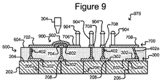
[0041] 図1のプロセス100を再び参照すると、ステップ112において、2つ以上のトレースを、その2つ以上のトレース間に配置されるトレースに電気的に接続することなく、電気的に接続する導電性ジャンパが形成されうる。図8及び図9は、導電性ジャンパ900が形成されうる一例を示す。図8及び図9に示される例では、トレース702及び706は、トレース704に電気的に接続することなくジャンパ900によって電気的に接続されうる。しかし、上記は一例に過ぎず、ジャンパ900といったジャンパは、トレース層700における他のトレースに接続するように形成されてもよい。図8及び図9には1つのジャンパ900が示されるが、より多くの又は少ないこのようなジャンパが形成されてもよい。
[0041] Referring again to the
[0042] 図8に示されるように、絶縁物質802が、電気的に接続されているトレース702及び706間(例えばトレース702及び706の端部間)の絶縁層600の表面604上に堆積されうる。さらに示されるように、絶縁物質802はさらに、ジャンパ900が電気的に接続されず、したがって電気的に迂回されるトレース704の一部上に堆積されうる。絶縁物質802は、電気的に接続されるべきトレース702及び706間の空間の少なくとも一部をほぼ充填しうるが、絶縁物質802は充填しなくてもよい。むしろ、いくつかの実施形態では、絶縁物質802は、トレース702及び706と絶縁物質802の一部に、トレース704に接触することなく、導電材料(図9では902)が堆積されうるのに十分なトレース704を覆うのでよい。
[0042] As shown in FIG. 8, an insulating
[0043] 絶縁物質802は、基板上に電気絶縁材料を堆積させるのに適した任意の方法で堆積されうる。いくつかの実施形態では、絶縁物質802は、流体さもなければプリント可能材料として堆積されうる。例えば絶縁物質802は(図3に関連して説明した)ディスペンサ304を介して施されうる。絶縁物質802は、液体状態、粘性状態、又はエアゾール状態でディスペンサ304を介して堆積され、その後、ほぼ固体状態に乾燥又は硬化されうる材料を含みうる。例えば絶縁物質802は、インク材料であってよい。絶縁物質802がインク材料であるかどうかに関係なく、絶縁物質802は、特定の材料に適した任意の方法で乾燥又は硬化されうる。例えば絶縁物質802は、周囲空気及び温度への露出によって、又は、熱又は硬化エネルギー源への露出によって乾燥又は硬化されうる。いくつかの実施形態では、絶縁物質802は、ディスペンサ304の使用以外の技術によって堆積されうる。このような技術は、絶縁物質802を、スピンコーティングによって、又は、ブラシ、スパチュラ(spatula)等といったアプリケータを用いて堆積することを含みうる。
[0043] The insulating
[0044] 図9に示されるように、導電性物質902が、電気的に接続されるべきトレース702及び706の一部(例えば端部)上に堆積されうる。さらに示されるように、導電性物質902はさらに、導電性物質902がトレース702及び706を、トレース702及び706間に少なくとも部分的に配置されるトレース704に接触することなく、そうでなければ電気的に接続することなく、電気的に接続するように、絶縁物質802上に堆積されうる。導電性物質902の堆積物は、上述したようにトレース302とほぼ同じであり、また、それらと同じ方法でかつ同じ1以上の材料で作られうる。例えば導電性物質902は、トレース302について可能な材料として上で特定された材料のいずれかを含み、また、導電性物質902は、トレース302を作成するために上で特定した方法のいずれでも堆積されうる。例えば導電性物質902は、導電性粒子(例えば銀、金、銅等の粒子又はナノ粒子)がその中で懸濁されるインク又は他の材料を含んでよく、また、導電性物質902は、液体状態、粘性状態又はエアゾール状態でディスペンサ304(例えばインクジェットプリントヘッドといったプリントヘッド又はエアゾール噴射機構)を介してトレース702及び704並びに絶縁物質802上に堆積されて、次に乾燥、そうでなければ硬化されうる。
[0044] As shown in FIG. 9, a conductive material 902 may be deposited on a portion (eg, end) of
[0045] 上述したように、ジャンパ900は、トレース層700における少なくとも2つのトレース(例えばトレース702及び706)を、これら少なくとも2つのトレース間に配置されたトレース(例えば704)に電気的に接続することなく、電気的に接続する単純で、高速、及び/又は効率的な方法でありうる。上で述べたとおり、トレース層700内の他のトレースを電気的に接続する2つ以上のそのようなジャンパ900がありうる。このようなジャンパ900は、トレース層内のトレースを電気的に接続するために追加の(例えば600のような)絶縁材料層及び(例えば402のような)ビア構造を必要とすることなく、同じトレース層(例えば700)においてトレース(例えば702及び706)間の電気的接続を与えうる。
[0045] As described above, the
[0046] 図3〜図10には示されていないが、ジャンパ900のような1以上のジャンパが配線基板202の表面204上に形成されて、トレース302のうちの2つ以上のトレースを、それら2つ以上のトレース302間のトレース302のうちの1つに電気的に接続することなく、電気的に接続しうる。したがって、ステップ112は、図1のプロセス100におけるステップ104の後にも行うことができる。
[0046] Although not shown in FIGS. 3-10, one or more jumpers, such as
[0047] 図1のプロセス100を再び参照すると、示されるように、ステップ106〜ステップ112のうちの1以上が、ステップ114においてプローブを設ける前に繰り返されうる。図10は、ステップ106〜ステップ112のうちの1以上が繰り返されて、(第1、第2等のビア構造の例であってよい)ビア構造1012が埋め込まれた(第1、第2、第3等のカスタマイズ層、又は、第1、第2、第3等の絶縁層の例であってよい)絶縁層100と、絶縁層1000の表面1004上の導電性トレース1052のトレース層1050とを含む追加のカスタマイズ層が形成される一例を示す。(トレース1052の層1050は、カスタマイズ層(例えば第1、第2、第3等のカスタマイズ層、又は、第1、第2、第3等のトレース層)の一例であってよい。)
[0047] Referring again to the
[0048] 図10に示されるように、ビア構造1012は、ステップ106においてトレース702、704、706、及び/又は708のうちの1以上に結合されうる。ビア構造1012は、ビア構造402と同様であってよく、またそれらと同じ方法で形成されうる。例えばビア構造1012は、上述したようにビア構造402が接合されたワイヤでありうるように接合されたワイヤを含みうる。別の例として、ビア構造1012は、図5に関して示されかつ上述したワイヤスタッド502のスタック504のようなワイヤスタッドのスタックを含みうる。図10に示されるように、1以上のビア構造1012は、ビア構造402aが配線基板202の表面204に対して角度が付けられているのとほぼ同じ方法で、絶縁層600の表面604に対して角度が付けられうる。
[0048] As shown in FIG. 10, via
[0049] 絶縁層1000は、絶縁材料602と同様でありうる電気絶縁材料1002を含みうる。例えば絶縁材料1002は、絶縁材料602に関して上述した材料のいずれかを含みうる。同様に、絶縁材料1002は、絶縁材料602が、配線基板202の表面204上に堆積されるかそうでなければ形成される上述した方法のいずれかにおいて表面604、トレース層700、及びジャンパ900上に堆積されるかさもなければ形成されうる。図6に関して上述したようにビア構造402の遠位端部606が絶縁材料層600の表面606に配置されるのとほぼ同じ方法で、ビア構造1012の遠位端部1016が、絶縁層1000の外面1004に配置されてよく、また、トレース層1050のトレース1052は、トレース層700のトレース702、704、706、及び/又は708がビア構造402の遠位端部606に電気的に接続されるのと同じ方法で遠位端部1016に電気的に接続されうる。(なお、絶縁層1000の外面1004は、上述したように絶縁層600の外面604が平坦化されるのと同じ方法で平坦化されうる。)トレース層1050のトレース1052は、上述したようにトレース302とほぼ同じであってよく、またそれらと同じ方法でかつ同じ1以上の材料で作られうる。例えばトレース1052は、トレース302について可能な材料として上で特定された材料のいずれかを含み、また、トレース1052は、トレース302を作成するために上で特定した方法のいずれでも作成されうる。図10には示されないが、ジャンパ900のような1以上のジャンパが、絶縁層1000の表面1004上に形成されて、トレース1052のうちの2つ以上を、ジャンパ(図示せず)によって接続された当該2つ以上のトレース1052間のトレース1052のうちの1つに電気的に接続することなく、電気的に接続しうる。
[0049] The insulating
[0050] 図1のプロセス100を再び参照すると、ステップ106〜ステップ112のうちの1以上が好きなだけ(0回から必要に応じた回数又は好きな回数であってよい)繰り返された後に、ステップ114において、導電性接点構造(例えばプローブ904)がトレース層700内のトレース702、704、706、及び/又は708のうちの1以上に結合される、及び/又はそれらの上に形成されうる。図9は、ステップ106〜ステップ112が1回行われ、ステップ114が行われてプローブ904がトレース702、704、706、及び/又は708のうちの1以上に結合される一例を示す。図10は、ステップ106〜ステップ112の一部又は全部が2回行われ、その後、ステップ114が行われてプローブ904がトレース1052のうちの1以上に結合される一例を示す。トレース702、704、706、及び/又は708に結合されているか、又はトレース1052に結合されているかに関わらず、プローブ904は、電子デバイス(図示せず)の端子(図示せず)と圧力に基づいた電気的接続を行うためのものでありうる。このような場合、プローブ904は、トレース702、704、706、及び/又は708、或いはトレース1052上に、接触されるべき端子(図示せず)に対応するパターンに配置されうる。プローブ904は、導電性のバネプローブ、ポスト、バンプ等であってよい。図9及び図10には4つのプローブ904が示されるが、より多くの又はより少ないプローブ904を用いてよい。さらに、図9及び図10におけるプローブ904のサイズ、形状、及びパターンは例に過ぎず、プローブ904は、図9又は図10に示されるものとは違うサイズ及び/又は形状であっても、及び/又は、違うパターンで配置されてもよい。
[0050] Referring again to the
[0051] いくつかの実施形態では、図1のプロセス100は、ベース配線基板上のカスタマイズ層がカスタム配置されたプローブへのカスタマイズされた電気的接続を与える、プローブヘッドといった多層配線基板を生成しうる。図9のプローブヘッド975は、そのようなプローブヘッドの一例でありうる。トレース層300、絶縁層600、トレース層700、及び/又はジャンパ900は、ベース配線基板202の接点208からカスタム配置されたプローブ904への電気的接続(電気的に接続されたトレース302、ビア構造402、トレース702、704、706、及び/又は708、及び/又はジャンパ900の組み合わせ)を与えるカスタマイズ層の例でありうる。なお、プローブ904は、プローブ904が電気的に接続される接点208のパターンとは異なるパターンにあってよい。
[0051] In some embodiments, the
[0052] 図10のプローブヘッド1075は、そのようなプローブヘッドの別の例でありうる。トレース層300、絶縁層600、トレース層700、絶縁層1000、ジャンパ900、及び/又は、トレース層1050は、ベース配線基板202の接点208からカスタム配置されたプローブ904への電気的接続(電気的に接続されたトレース302、ビア構造402、トレース702、704、706、及び/又は708、ジャンパ900、ビア構造1012、及び/又は、トレース1052の組み合わせ)を与えるカスタマイズ層の例でありうる。再度言及するが、プローブ904は、プローブ904が電気的に接続される接点208のパターンとは違うパターンにあってよい。
[0052] The
[0053] 以下において分かるように、プローブヘッド975及び1075は、(以下に説明する)図18及び図19におけるプローブカードアセンブリ1814と同様のプローブカードアセンブリの一部でありうるプローブヘッドの例でありうる。図9及び図10のプローブヘッド975及び1075は例に過ぎず、他のタイプの電子デバイスを、図1のプロセス100を用いて作成しうる。例えば図1のプロセス100の他のステップのうちでもステップ114は、任意選択的であってよく、行わなくてもよく、及び/又は、別のステップに取って代わられてもよい。例えばステップ114は行われなくてもよく、したがってプローブ904が任意のトレースに結合される必要もなく又はさらには存在しなくてもよい。別の例として、ステップ114においてプローブ904をトレースに結合するのではなく、1以上の別のタイプの電子構造をトレースに結合させうる。例えば抵抗、コンデンサ、トランジスタといった電子回路素子(図示せず)がトレース(例えばトレース702、704、706、及び/又は708、或いは1052)に結合されうる。いくつかの実施形態では、例えば抵抗(図示せず)がトレースを接地に電気的に接続するように抵抗(図示せず)がトレース702、704、706、及び/又は708、或いは1052に結合されうる。別の例として、抵抗がトレース702、704、706、及び/又は708、或いは1052に結合され、また、抵抗が、事実上、プローブ904へのトレースを通る電気経路において直列構成にあるようにプローブ904がトレースに結合される。上記に関係なく、このような電子回路素子(図示せず)は、トレース302を形成するために上述した技術化のいずれかを用いて形成されうる。例えば抵抗を形成する1以上の抵抗は、インク材料か、又は、所望の導電率(又は電気抵抗)を有する導電性粒子がその中に懸濁されている材料でありうる。このようなインク材料は、液体状態、粘性状態又はエアゾール状態においてディスペンサ304によって堆積され、堆積後に乾燥されうる。
[0053] As will be seen below, probe heads 975 and 1075 are examples of probe heads that may be part of a probe card assembly similar to probe
[0054] 別の例として、図1のプロセス100のうち特にステップ112は、任意選択であってよく、従って、ジャンパ900は作成されなくても又は含まれなくてもよい。
[0054] As another example, particularly step 112 of
[0055] 図11は、本発明のいくつかの実施形態に従って、ベース配線基板に1以上のカスタマイズ層を追加するための別のプロセス1100を示す。説明及び議論の便宜上、プロセス1100は、カスタマイズ層がベース配線基板202に追加される図12〜図17に示される例について以下に述べられる。しかし、プロセス1100は、図12〜図17に示される例に限定されない。
[0055] FIG. 11 illustrates another
[0056] 図11を参照すると、ステップ1102は、図2に関して上述したベース配線基板202であってよいベース配線基板を得ることを含みうる。図12に示されるように、配線基板202は、導電性トレース1202を含むトレース層1200を含みうる。配線基板202は、ステップ1102において、トレース1202がその上に既に形成されている状態で得られてもよいし、或いは、ステップ1102は、配線基板202の表面204上にトレース1202を形成することを含んでもよい。トレース1202は、上述したようにトレース302とほぼ同じであってよく、またそれらと同じ方法でかつ同じ1以上の材料で作成されうる。例えばトレース1202は、トレース302について可能な材料として上で特定された材料のいずれかを含み、またトレース302を作成するために上で特定した方法のいずれでも作成されうる。図12には5つのトレース1202が示されるが、より多くの又はより少ないトレース1202があってよい。さらに、図12におけるトレース1202の形状、サイズ、及び配置は例に過ぎず、トレース1202は、異なる形状及び/又はサイズを有してよく、また、異なるパターンに配置されうる。トレース1202の層1200は、カスタマイズ層(例えば第1、第2、第3等のカスタマイズ層、又は、第1、第2、第3等のトレース層)の一例でありうる。
Referring to FIG. 11,
[0057] 図11のプロセス1100を再び参照すると、ステップ1104において、絶縁層及びトレース層を含むカスタマイズ層が、配線基板上に形成されうる。図13は、電気絶縁材料1302の絶縁層1300と、複数の導電性トレース1352を含むトレース層1350とが、配線基板202上に形成されうる一例を示す。トレース1352の層1350はカスタマイズ層(例えば第1、第2、第3等のカスタマイズ層、又は、第1、第2、第3等のトレース層)の一例であってよく、絶縁層1300はカスタマイズ層(例えば第1、第2、第3等のカスタマイズ層、又は、第1、第2、第3等の絶縁層)の一例であってよい。
[0057] Referring again to the
[0058] 絶縁材料1302は、多少あるが限定された粘性を有する接着フィルム(例えばBステージエポキシフィルムといったエポキシフィルム)を含みうる。このような接着フィルムの形態の絶縁材料1302は、配線基板202の表面204上とトレース1202上に配置されうる。導電材料(例えば金、銀、銅等といった金属)のシートが、(接着フィルムの形態の)絶縁材料1302の外面1304上に配置されて、十分かつほぼ均一な圧力が導電材料シートに加えられて、それにより(接着フィルムの形態の)絶縁材料1302がトレース1202の周りに流れるようにしうる。(接着フィルムの形態の)絶縁材料1302は、絶縁材料1302が配線基板202の表面204と、絶縁材料1302の外面1304上にある導電材料シートの両方に接着するように硬化されるかそうでなければ固められる。いくつかの実施形態では、絶縁材料1302は、配線基板202の表面204上に配置される前又は配置された直後に、軟化点にまで加熱されてよく、その後、絶縁材料1302は、絶縁材料1302を周囲温度にまで冷却させることによって硬化されうる。
[0058] The insulating
[0059] 上記に関係なく、絶縁材料1302が硬化された後、絶縁材料1302の表面1304上の導電材料シートは、トレース1352を形成するようにパターン付けされうる。例えば導電材料シートの一部が選択的に除去されて、トレース1352が残されうる。いくつかの実施形態では、導電材料シートの一部が絶縁材料1302から(例えばレーザを用いて)緩められて絶縁材料1302から(例えばエアブラスト、握りツール等を用いて緩められた部分に力を加えることによって)除去されうる。或いは、又は、さらには、絶縁材料1302の表面1304に接着された導電材料シートの一部が、ミリングマシン、化学エッチング等といった他の方法で除去されうる。形成方法に関係なく、トレース1352は、以下において分かるように、トレース1202及びプローブ1504へのビア構造1500(図15参照)、又は、トレース層1600への別のビア構造1750(図17参照)が形成される、絶縁層1300の表面1304上の位置に配置されうる。
[0059] Regardless of the above, after the insulating
[0060] 或いは、絶縁層1300は、上述したように絶縁層600と同じ方法のいずれかで、かつ、それと同じ材料のいずれかで形成されうる。同様に、トレース1352は、上述したようにトレース302と同じ方法のいずれかで、かつ、それらと同じ材料のいずれかで形成されうる。例えばトレース1352は、トレース302について可能な材料として上で特定された材料のいずれかを含み、また、トレース1352は、トレース302を作成するために上で特定した方法のいずれでも作成されうる。
[0060] Alternatively, the insulating
[0061] 図11のプロセス1100を再び参照すると、ステップ1106及びステップ1108においてトレース(例えば1202)のうちのいくつかを、トレース(例えば1352)のうちのいくつかに電気的に接続する導電性ビア構造が形成されうる。図14及び図15は、図11のプロセス1100のステップ1106において絶縁層1300内に開口1402を作成し、次に図11のステップ1108において各開口1402の傾斜された側壁1404上に導電性物質1502を堆積させることによって、(第1、第2等のビア構造の例であってよい)導電性ビア構造1500が形成される一例を示す。
[0061] Referring again to the
[0062] 図14に示されるように、各開口1402は、トレース1352のうちの1つに隣接して形成され、絶縁層1300内を延在し、トレース1202のうちの1つの一部を露出させる。各開口1402は、トレース1352に隣接する傾斜側壁1404を有しうる。傾斜側壁1404は、配線基板202の表面204に垂直な軸1406に対して角度を有するように傾斜されうる。いくつかの実施形態では、角度は少なくとも15度でありうる。他の実施形態では、角度は、少なくとも10度、少なくとも20度、少なくとも30度、又は少なくとも45度でありうる。上記角度数値は例に過ぎず、本発明はこれらの角度数値のいずれにも必ずしも限定されない。
[0062] As shown in FIG. 14, each
[0063] 開口1402は、絶縁材料1302に開口を形成するのに適した任意の方法で形成されうる。いくつかの実施形態では、レーザ1408が、絶縁材料1302内に開口1402を刻み込みうる。そのような場合、トレース1202は、レーザ1408が配線基板202内へと刻み込むことを防ぐ機能を有しうる。或いは、化学エッチング、機械的切断等を含む他の技術を用いて開口1402を形成しうる。
[0063] The
[0064] 図15に示されるように、各ビア構造1500は、開口1402によって露出されているトレース1202の一部、開口1402の側壁1404、及び開口1402に隣接するトレース1352の一部上に導電性基板1502を堆積させることによって形成されうる。導電性物質1502は、上述したトレース302と同じ1以上の材料であってよく、また、上述したようにトレース302と同じ方法で堆積されうる。例えば導電性物質1502は、トレース302について可能な材料として上で特定された材料のいずれかを含んでもよく、また、導電性物質1502は、トレース302を形成するために上で特定した方法のいずれでも堆積されかつ硬化されうる。例えば導電性物質1502は、導電性材料(例えば金、銀、銅等)の粒子又はナノ粒子がその中に懸濁されるインクを含んでよく、インクはディスペンサ304(例えばインクジェットプリントヘッドといったプリントヘッド又はエアゾール噴射機構)を介して堆積されてよく、次に、乾燥されるかそうでなければ硬化される又は固められうる。作成方法に関係なく、各ビア構造1500は、トレース層1200のトレース1202のうちの1つを、トレース層1350のトレース1352のうちの1つに電気的に接続しうる。いくつかの実施形態では、また、上述しかつ図面に示された例の代替として、トレース1352は、開口1402が形成された後に形成されてよく、また、トレース1352は、ビア構造1500と同時に、それと同じ材料で、また同じ方法で形成されてよく、さらには絶縁層1300の表面1304上のビア構造1500の延長部であってよい。
[0064] As shown in FIG. 15, each via
[0065] 図11のプロセス1100を再び参照すると、示されるように、ステップ1110においてプローブが設けられる前に、ステップ1104〜ステップ1108のうちの1回以上が繰り返されうる。図16及び図17は、絶縁層1600、絶縁層1600の表面1604上のトレース1652の層1650、及びビア構造1750を含む追加のカスタマイズ層を形成するようステップ1104〜ステップ1108が繰り返されうる例を示す。絶縁層1600を通る開口1702内の(第1、第2等のビア構造の例でありうる)導電性ビア構造1750は、トレース1652のうちのいくつかをトレース1352のうちのいくつかに電気的に接続しうる。
[0065] Referring again to process 1100 of FIG. 11, as shown, one or more of
[0066] 図16は、図11のプロセス1100のステップ1104が繰り返されて、絶縁層1300及びトレース層1350上に絶縁層1600及びトレース層1650が形成される一例を示す。トレース層1650は、カスタマイズ層(例えば第1、第2、第3等のカスタマイズ層、又は、第1、第2、第3等のトレース層)の一例であってよく、絶縁層1600はカスタマイズ層(例えば第1、第2、第3等のカスタマイズ層、又は、第1、第2、第3等の絶縁層)の一例であってよい。
FIG. 16 illustrates an example where
[0067] 絶縁層1600の絶縁材料1602は、多少あるが限定された粘性を有する接着フィルム(上述したように絶縁材料1302と同じ材料を含みうる)を含みうる。(接着フィルムの形態の)絶縁材料1602は、絶縁層1300及びトレース層1350上に堆積されうる。導電材料(例えば金、銀、銅等といった金属)のシートを(接着フィルムの形態の)絶縁材料1602の外面1604上に配置させ、十分かつほぼ均一な圧力を導電材料シートに加え、それにより、図16に全体に示されるように、(接着フィルムの形態の)絶縁材料1602がトレース1352及びビア構造1500の周りに全体的に、かつ絶縁層1300における開口1402内に流れるようにしうる。図16には示されないが、表面1604は平面でなくともよい。例えば表面1604は、トレース1352に接続されたビア構造1500の一部の上方で隆起しうる。
[0067] The insulating
[0068] (接着フィルムの形態の)絶縁材料1602は、(接着フィルムの形態の)絶縁材料1602がトレース1352、ビア構造1500及び絶縁層1300、並びに絶縁材料1602の外面1604上の導電材料シートに接着するように硬化されるかそうでなければ固められうる。いくつかの実施形態では、(接着フィルムの形態の)絶縁材料1602は、トレース1352及びビア構造1500上、並びに絶縁材料1300における開口1402内に配置される前又は配置された直後に軟化点にまで加熱されてよく、その後、(接着フィルムの形態の)絶縁材料1602は、絶縁材料1602を周囲温度にまで冷却させることによって硬化されうる。
[0068] Insulating material 1602 (in the form of an adhesive film) is a conductive material sheet on insulating material 1602 (in the form of an adhesive film) traces 1352, via
[0069] 上記に関係なく、絶縁材料1602が硬化された後、絶縁材料1602の表面1604に接着された導電材料シートは、トレース1652を形成するようにパターン付けされうる。例えば導電材料シートの一部が選択的に除去されて、トレース1652が残されうる。これは、トレース1352を形成するために上述した方法のいずれでも実現可能であり、したがってトレース1652が形成されうる。形成方法に関係なく、トレース1652は、以下において分かるように、プローブ1504(図17参照)又はトレース1650の上方に形成されるトレース層(図示せず)への別のビア構造(図示せず)が形成される、絶縁層1600の表面1604上の位置に配置されうる。
[0069] Regardless of the above, after the insulating
[0070] 或いは、絶縁層1600は、上述したように絶縁層600と同じ方法で、かつ、同じ材料で形成されうる。同様にトレース1652は、上述したようにトレース302と同じ方法のいずれでも、かつ、それと同じ材料のいずれでも形成されうる。例えばトレース1652は、トレース302について可能な材料として上で特定された材料のいずれかを含み、また、トレース1652は、トレース302を作るために上で特定した方法のいずれでも作成されうる。
Alternatively, the insulating
[0071] 図17は、ステップ1106を繰り返して絶縁層1600内に開口1702が形成され、ステップ1108を繰り返してトレース1652のうちのいくつかをトレース1352及び/又はビア構造1500のうちのいくつかに電気的に接続するビア構造1750が形成される一例を示す。開口1702は、図14に関して上述したような開口1402とほぼ同じであってよく、また、それらとほぼ同じ方法で形成されうる。ビア構造1750は、図15に関して上述したようなビア構造1500とほぼ同じであってよく、また、それらとほぼ同じ方法で形成されうる。さらに、ビア構造1750は、図15に関して上述したように導電物質1502と同じであってよく、また、それらと同じ方法で堆積されて硬化又は乾燥されうる導電物質1752を含みうる。トレース1352に関して上述したように、いくつかの実施形態では、また、上述しかつ図面に示された例の代替として、トレース1652は、開口1702が形成された後に形成されてよく、また、トレース1652は、ビア構造1750と同時に、それと同じ材料で、また同じ方法で形成されてよく、さらには絶縁層1600の表面1604上のビア構造1750の延長部であってよい。
[0071] FIG. 17 illustrates that
[0072] 図11のプロセス1100を再び参照すると、ステップ1102〜ステップ1108が好きなだけ(0回から必要に応じた回数又は好きな回数であってよい)繰り返された後に、ステップ1110において、導電性接点構造(例えばプローブ1504)が、カスタマイズ層の外面上の1以上のトレースに結合される及び/又はそれらの上に形成されうる。図15は、ステップ1102〜ステップ1108が1回行われ、ステップ1110が行われてプローブ1504がトレース1352のうちの1以上に結合される一例を示す。図16は、ステップ1102〜ステップ1108が2回行われて、次にステップ1110が行われて、プローブ1504がトレース1652のうちの1以上に結合される一例を示す。
[0072] Referring again to the
[0073] トレース1352に結合されているか、又はトレース1652に結合されているかに関わらず、プローブ1504は、電子デバイス(図示せず)の端子(図示せず)との圧力に基づいた電気的接続を行うためのものでありうる。その場合、プローブ1504は、接触されるべき端子(図示せず)に対応するトレース1352又は1652上のパターンに配置されうる。プローブ1504は、プローブ904について上述したプローブのいずれかと同様でありうる。図15には5つのプローブ1504が示され、図16には3つのプローブ1504が示されるが、より多くの又は少ないプローブ904が用いられてもよい。さらには、図15及び図16におけるプローブ1504のサイズ、形状、及びパターンは例に過ぎず、プローブ1504は図15又は図16に示されるものとは違うサイズ及び/又は形状であっても、及び/又は、違うパターンで配置されてもよい。図12〜図17には示されないが、図9のジャンパ900と同様の1以上のジャンパが、図11のプロセス1100の一部として形成されて、図12〜図17のトレース層1200、1350、及び/又は1650のいずれかにおけるトレースを電気的に接続しうる。したがって、図1のステップ112は、図11のプロセス1100においても行われうる。
[0073] Regardless of whether it is coupled to trace 1352 or to trace 1652,
[0074] いくつかの実施形態では、図11のプロセス1100は、ベース配線基板上のカスタマイズ層がカスタム配置されたプローブへのカスタマイズされた電気的接続を与える、プローブヘッドといった多層配線基板を生成しうる。図15のプローブヘッド1575は、そのようなプローブヘッドの一例でありうる。トレース層1200、絶縁層1300、ビア構造1500、及び/又はトレース層1350は、ベース配線基板202の接点208からカスタム配置されたプローブ1504への電気的接続(電気的に接続されたトレース1202、ビア構造1500及びトレース1352の組み合わせ)を与えるカスタマイズ層の例でありうる。なお、プローブ1504は、プローブ904が電気的に接続される接点208のパターンとは異なるパターンにあってよい。
[0074] In some embodiments, the
[0075] 図17のプローブヘッド1775は、別のそのようなプローブヘッドの一例でありうる。トレース層1200、絶縁層1300、ビア構造1500、トレース層1350、絶縁層1600、ビア構造1750、及び/又はトレース層1650は、ベース配線基板202の接点208からカスタム配置されたプローブ1504への電気的接続(電気的に接続されたトレース1202、ビア構造1500、トレース1352、ビア構造1750及びトレース1652の組み合わせ)を与えるカスタマイズ層の例でありうる。なお、プローブ1504は、プローブ904が電気的に接続される接点208のパターンとは異なるパターンにあってよい。
[0075] The probe head 1775 of FIG. 17 may be an example of another such probe head.
[0076] 以下において分かるように、プローブヘッド1575及び1775は(以下に説明する)図18及び図19におけるプローブカードアセンブリ1814と同様のプローブカードアセンブリの一部でありうるプローブヘッドの例でありうる。図15及び図17のプローブヘッド1575及び1775は例に過ぎず、他のタイプの電子デバイスを、図11のプロセス1100を用いて作成しうる。例えば図11のプロセス1100の他のステップのうちでもステップ1110は、任意選択的であってよく、行わなくてもよく、及び/又は、別のステップに置き換えられてもよい。例えばステップ1110は行わなくてもよく、したがってプローブ1504は任意のトレースに結合される必要もなく又は存在しなくてもよい。別の例として、ステップ1110において、プローブ1504をトレースに結合するのではなく、1以上の別のタイプの電子構造をトレースに結合してもよい。例えば抵抗、コンデンサ、トランジスタ等といった電子回路素子(図示せず)がトレース(例えばトレース1352又は1652)に結合されうる。
[0076] As will be seen below, probe heads 1575 and 1775 may be examples of probe heads that may be part of a probe card assembly similar to probe
[0077] 上記の通り、図1及び図11のプロセス100及び1100は、ベース配線基板上に、ベース配線基板上又は内のビア又は他の電気的接点構造から、プローブといったカスタム配置された電気素子へのカスタマイズされた電気的接続を与えるカスタマイズ層を形成する例を示す。このようなカスタマイズされたベース配線基板には多くの実用的な用途がある。図18は、図1のプロセス100又は図11のプロセス1100によりカスタマイズされたベース配線基板が生成されて、プローブカードアセンブリ1800の構成要素として使用されうる、かかる用途の一例を示す。以下において分かるように、プローブカードアセンブリ1800は、図1のプロセス100又は図11のプロセス1100に従って配線基板202に1以上のカスタマイズ層1812が追加されたベース配線基板202を含みうるプローブヘッド1818を含みうる。
[0077] As described above, the
[0078] 図18は、1以上の半導体ダイ(例えばダイがその上に作られたウェーハから単体化される又は単体化されていない、パッケージ化される又はパッケージ化されていない)又は入力及び/又は出力端子1822を有する他の電子デバイスといった1以上の試験用電子デバイスでありうるDUT1820を試験するように用いられうるプローブカードアセンブリ1800の一例を示す。図18に示されるように、プローブカードアセンブリ1800は、配線基板1802、電気コネクタ1808、及びプローブヘッド1818を含んでよく、これらはすべて互いに(例えば、クランプ、ボルト、ネジ等(図示せず)によって)機械的に結合されうる。導電性プローブ1816は、DUT1820の端子1822の少なくともいくつかに対応するパターンで、プローブヘッド1818上に配置されうる。プローブ1816は、端子1822と電気的に接続するようにDUT1820の端子1822に押し付けられると、主に弾性的挙動を示しうる。6つのプローブ1816及び6つの端子1822が示されるが、より多くても少なくてもよい。さらに、いくつかの実施形態では、端子1822より少ないプローブ1816があってよく、したがって、その場合、すべての端子1822に接触するようプローブ1816は複数の端子1822に接地しうる。プローブヘッド1818を通るカスタム電気的接続1814及びビア206と、電気コネクタ1808を通る電気的接続1810と、配線基板1802を通る電気的接続1806は、プローブ1816を、配線基板1802上の電気的インタフェース1804に電気的に接続しうる。
[0078] FIG. 18 illustrates one or more semiconductor dies (eg, singulated or not singulated, packaged or unpackaged) from the wafer on which the dies are fabricated, input and / or Or shows an example of a
[0079] 電気的インタフェース1804は、図19における試験コントローラ1902と同様の試験コントローラ(図示せず)への及びそこからの個々の通信チャネルに接続されうる複数の電気コネクタを含みうる。例えば電気的インタフェース1804は、ゼロ挿入力(ZIF)電気コネクタ、ポゴピンパッド又は他のそのような電気コネクタを含みうる。配線基板1802は、プリント回路基板等といった剛性又は半剛性配線基板でありうる。配線基板1802を通る電気接続1806は、配線基板1802上及び/又は内の導電性ビア及び/又はトレースでありうる。電気コネクタ1808は、電気的接続1806のうちのいくつかとプローブヘッド1818との間の複数の電気的接続1810を含みうる。電気的コネクタ1808は、電気的接続1806をプローブヘッド1818に接続するのに適した任意のデバイス又は電気コネクタの集まりでありうる。例えば電気コネクタ1808は、インターポーザ、ワイヤ、はんだ等を含みうる。
[0079] The
[0080] プローブヘッド1818は、上述したベース配線基板202と、配線基板202の表面204上又は表面における接点208からカスタム配置されたプローブ1816へのカスタム電気的接続1814を与える1以上のカスタマイズ層1812とを含みうる。プローブ1816は、プローブ1816が端子1822のうちの少なくともいくつかと位置合わせされ、従って接触するようにDUT1820の端子1822の少なくともいくつかの端子のパターンに対応するパターンに配置されうる。
[0080] The
[0081] いくつかの実施形態では、カスタマイズ層1812及びプローブ1816は、図1のプロセス100を用いてベース配線基板202に追加されうる。したがって、プローブヘッド975は、図18のプローブヘッド1818の一例であってよく、したがって、プローブヘッド975は、図18のプローブヘッド1818に取って代わりうる。その場合、図9におけるトレース層300及び700、絶縁層600、ビア構造402及びジャンパ900は、図18におけるカスタマイズ層1812の例であり、図9におけるプローブ904は、図18におけるプローブ1816の一例であり、また、図9における、接点208のうちの1つをプローブ904のうちの1つに電気的に接続する、電気的に接続されたトレース302、ビア構造402、ジャンパ900及び/又はトレース702は、図18におけるカスタム電気的接続1814の例でありうる。
[0081] In some embodiments,
[0082] 同様に、プローブヘッド1075は、図18におけるプローブヘッド1818の別の例でありうる。したがって、プローブヘッド1075は、図18のプローブヘッド1818に取って代わりうる。その場合、図10におけるトレース層300、700及び1050、絶縁層600及び1000、ビア構造402及び1012及びジャンパ900は、図18におけるカスタマイズ層の一例でありうる。同様に、図10におけるプローブ904は、図18におけるプローブ1816の一例でありうる。図10における、接点208のうちの1つをプローブ904のうちの1つに電気的に接続する、電気的に接続されたトレース302、ビア構造402、トレース702、ジャンパ900、ビア構造1012及びトレース1052は、図18におけるカスタム電気的接続1814の例でありうる。
[0082] Similarly,
[0083] 或いは、いくつかの実施形態では、カスタマイズ層1812及びプローブ1816は、図11のプロセス1100を用いてベース配線基板202に追加されうる。したがって、図15のプローブヘッド1575は、図18におけるプローブヘッド1818の一例であってよく、したがって、プローブヘッド1575は、図18におけるプローブヘッド1818に取って代わりうる。そのような場合、図15におけるトレース層1200及び1350、絶縁層1300及びビア構造1500は、図18におけるカスタマイズ層1812の例であってよく、図15におけるプローブ1504は、図18におけるプローブ1816の例でありうる。また、図15における、接点208のうちの1つをプローブ1504のうちの1つに電気的に接続する、電気的に接続されたトレース1202、ビア構造1500及びトレース1532は、図18におけるカスタム電気接続1814の例でありうる。
[0083] Alternatively, in some embodiments,
[0084] 同様に、図17のプローブヘッド1775は、図18におけるプローブヘッド1818の別の例であってよく、したがって、プローブヘッド1775は、図18のプローブヘッド1818に取って代わりうる。そのような場合、図17における、トレース層1200、1350及び1650、絶縁層1300及び1600及びビア構造1500及び1750は、図18におけるカスタマイズ層1812の例でありうる。同様に、図17におけるプローブ1504は、図18におけるプローブ1816の例でありうる。図17における、接点208のうちの1つをプローブ1504のうちの1つに電気的に接続する、電気的に接続されたトレース1202、ビア構造1500、トレース1352、ビア構造1750及びトレース1652は、図18におけるカスタム電気的接続1814の例でありうる。
[0084] Similarly, the probe head 1775 of FIG. 17 may be another example of the
[0085] 図18のプローブカードアセンブリは、次の通りに作成されうる。試験されるDUT1820の端子1822の位置に関する情報が受信されうる。端子1822の位置に必ずしも対応しない接点208のパターンを有するベース配線基板202が入手されうる。(接点208は、DUT1820の端子1822に対応する必要がないので、端子1822の位置についての情報を受信する前にベース配線基板202を入手してもよい。)図1のプロセス100、図11のプロセス1100、又は同様のプロセスに従って、配線基板202の接点208から、端子1822の位置に関する情報に従ってプローブ1816をDUT1820の端子1822に位置合わせするパターンに配置されうる、プローブ1816へのカスタム電気的接続1814を与えるカスタマイズ層1812が、ベース配線基板202に追加されうる。したがって、プローブ1816のパターンは、DUT1820の端子1822のパターンに対応するようにカスタマイズされうる。
[0085] The probe card assembly of FIG. 18 may be made as follows. Information regarding the location of the
[0086] 図19は、本発明のいくつかの実施形態に従って、DUT1820を試験するためにプローブカードアセンブリ1800を用いうる試験システム1900の一例を示す。図19に示されるように、試験システム1900は、DUT1820に入力信号を提供でき、また、入力信号に呼応してDUT1820により生成される応答信号を受信しうる試験コントローラ1902を含みうる。「試験信号」との用語は、一般的に、試験コントローラ1902によって生成された入力信号及びDUT1820によって生成された応答信号の片方又は両方を指しうる。プローブカードアセンブリ1800は、試験システム1900のハウジング1920(例えばプローバー)のマウント機構1910に結合されうる。プローブカードアセンブリ1800のプローブ1816は、DUT1820の端子1822と圧力に基づいて電気的に接続して、試験信号が試験コントローラ1902とDUT1820との間で通信接続1904(例えば同軸ケーブル、ワイヤレスリンク、光ファイバーリンク等)、試験ヘッド1906内の電子機器(図示せず)、試験ヘッド1906と電気的インタフェース1804との間の電気的接続1908、及びプローブカードアセンブリ1800を介して送られうる。
[0086] FIG. 19 illustrates an example of a test system 1900 that may use a
[0087] DUT1820は以下の通りに試験されうる。プローブカードアセンブリ1800は、ハウジング1920のマウント機構1910に結合され、DUT1820の端子1822は、プローブカードアセンブリ1800のプローブ1816に接触しうる。これは、その上にDUT1820が配置されるチャック1924を、DUT1820の端子1822がプローブカードアセンブリ1800のプローブ1816に押し付けられるように動かすことにより達成されうる。或いは、プローブカードアセンブリ1800、又は、チャック1924及びプローブカードアセンブリ1800の両方が動かされて、端子1822とプローブ1816とを接触させうる。
[0087]
[0088] プローブ1816及び端子1822が接触している間、DUT1820は、プローブカードアセンブリ1800を介して試験コントローラ1902とDUT1820との間で試験信号(上述したように、試験コントローラ1902によって生成された入力信号と、入力信号に呼応してDUT1820によって生成された応答信号を含みうる)を提供することによって試験されうる。試験コントローラ1902は、応答信号を分析して、DUT1820が試験を合格しているかどうかを判定する。例えば試験コントローラ1902は、応答信号を期待応答信号と比較しうる。応答信号が期待応答信号と一致する場合には、試験コントローラ1902は、DUT1820が試験を合格したと判定しうる。そうでなければ、試験コントローラ1902は、DUT1820が試験に不合格であったと判定しうる。別の例として、試験コントローラ1902は、応答信号が許容範囲内にあるかどうかを判定し、範囲内にある場合には、DUT1820が試験に合格したと判定しうる。
[0088] While the
[0089] 図18のプローブカードアセンブリ1800及び図19の試験システム1900は例に過ぎない。例えば図9のプローブヘッド975、図10のプローブヘッド1075、図16のプローブヘッド1675及び図17のプローブヘッド1775は、異なるプローブカードアセンブリ又は試験コンタクタといった他の電子デバイスにおいて用いられうる。別の例として、図18のプローブカードアセンブリ1800は、他の試験システムにおいて用いられうる。
[0089] The
[0090] 本明細書において本発明の特定の実施形態及び用途を記載したが、これらの実施形態及び用途は例に過ぎず、多くのバリエーションが可能である。 [0090] Although specific embodiments and applications of the invention have been described herein, these embodiments and applications are merely examples and many variations are possible.
Claims (14)
前記ベース基板の表面上に配置された第1導電性トレース層と、
前記第1導電性トレース層上に配置されかつ前記ベース基板の前記表面に結合された第1電気絶縁材料剛性層と、
前記第1電気絶縁材料剛性層内に埋め込まれた導電性の第1ビアと、
前記ベース基板上および前記第1電気絶縁材料剛性層の外面上に形成された複数のジャンパと、
前記第1電気絶縁材料剛性層上に配置された第2導電性トレース層と、
を含み、
前記第1ビアの各々は、前記第1導電性トレース層のトレースのうちの1つに接合され、前記第1電気絶縁材料剛性層の前記外面まで延在するワイヤスタッドのスタック又はワイヤを含み、
前記ジャンパは、前記第1導電性トレース層の前記トレースのうち、少なくとも二つのトレースを接続し、前記第2導電性トレース層のトレースのうち、少なくとも二つのトレースを接続する、
多層配線基板。 A base substrate;
A first conductive trace layer disposed on a surface of the base substrate;
A first electrically insulating material rigid layer disposed on the first conductive trace layer and bonded to the surface of the base substrate;
A conductive first via embedded in the first electrically insulating material rigid layer;
A plurality of jumpers formed on the base substrate and on an outer surface of the first electrically insulating material rigid layer;
A second conductive trace layer disposed on the first electrically insulating material rigid layer;
Including
Each of the first vias includes a stack or wire of wire studs bonded to one of the traces of the first conductive trace layer and extending to the outer surface of the first electrically insulating material rigid layer ;
The jumper of the trace of the first conductive trace layer, connecting at least two traces, among the traces of the second conductive trace layer, connecting at least two traces,
Multilayer wiring board.
前記第2電気絶縁材料層内に埋め込まれた導電性の第2ビアであって、前記第2ビアの各々は、前記第2導電性トレース層の前記トレースのうちの1つに接合されかつ前記第2電気絶縁材料層の外面まで延在するワイヤスタッドのスタック又はワイヤを含む、請求項6に記載の多層配線基板。 A second electrically insulating material layer disposed on the outer surface of the second conductive trace layer and the first electrically insulating material rigid layer;
Conductive second vias embedded in the second electrically insulating material layer, each of the second vias being bonded to one of the traces of the second conductive trace layer and stack or wires including wires studs extending to the outer surface of the second electrically insulating material layer, a multilayer wiring board according to claim 6.
Applications Claiming Priority (3)
| Application Number | Priority Date | Filing Date | Title |
|---|---|---|---|
| US12/719,136 | 2010-03-08 | ||
| US12/719,136 US8476538B2 (en) | 2010-03-08 | 2010-03-08 | Wiring substrate with customization layers |
| PCT/US2011/026960 WO2011112409A2 (en) | 2010-03-08 | 2011-03-03 | Wiring substrate with customization layers |
Publications (3)
| Publication Number | Publication Date |
|---|---|
| JP2013522874A JP2013522874A (en) | 2013-06-13 |
| JP2013522874A5 JP2013522874A5 (en) | 2014-04-17 |
| JP6087630B2 true JP6087630B2 (en) | 2017-03-01 |
Family
ID=44530323
Family Applications (1)
| Application Number | Title | Priority Date | Filing Date |
|---|---|---|---|
| JP2012557087A Expired - Fee Related JP6087630B2 (en) | 2010-03-08 | 2011-03-03 | Wiring board with customized layer |
Country Status (5)
| Country | Link |
|---|---|
| US (1) | US8476538B2 (en) |
| JP (1) | JP6087630B2 (en) |
| KR (1) | KR101851269B1 (en) |
| TW (1) | TWI533775B (en) |
| WO (1) | WO2011112409A2 (en) |
Families Citing this family (9)
| Publication number | Priority date | Publication date | Assignee | Title |
|---|---|---|---|---|
| US9484973B1 (en) * | 2010-08-09 | 2016-11-01 | Qorvo Us, Inc. | Voltage equalization for stacked FETs in RF switches |
| TW201228507A (en) * | 2010-12-17 | 2012-07-01 | Hon Hai Prec Ind Co Ltd | Printed circuit board |
| TW201347124A (en) * | 2012-05-07 | 2013-11-16 | 矽品精密工業股份有限公司 | Semiconductor package and method for fabricating the same |
| JP2014216123A (en) * | 2013-04-24 | 2014-11-17 | タイコエレクトロニクスジャパン合同会社 | Electric connector assembly and mounting structure thereof |
| US9431759B2 (en) | 2014-10-20 | 2016-08-30 | HGST Netherlands B.V. | Feedthrough connector for hermetically sealed electronic devices |
| US10650181B2 (en) * | 2017-09-21 | 2020-05-12 | Nokia Solutions And Networks Oy | Spatial location of vias in a printed circuit board |
| CN111566806B (en) * | 2018-01-24 | 2024-04-30 | 京瓷株式会社 | Wiring substrate, electronic device, and electronic module |
| US10790307B2 (en) | 2018-11-27 | 2020-09-29 | Qorvo Us, Inc. | Switch branch structure |
| WO2021178238A1 (en) * | 2020-03-02 | 2021-09-10 | Kuprion Inc. | Ceramic-based circuit board assemblies formed using metal nanoparticles |
Family Cites Families (43)
| Publication number | Priority date | Publication date | Assignee | Title |
|---|---|---|---|---|
| US4771537A (en) * | 1985-12-20 | 1988-09-20 | Olin Corporation | Method of joining metallic components |
| US5229549A (en) * | 1989-11-13 | 1993-07-20 | Sumitomo Electric Industries, Ltd. | Ceramic circuit board and a method of manufacturing the ceramic circuit board |
| US5310965A (en) * | 1991-08-28 | 1994-05-10 | Nec Corporation | Multi-level wiring structure having an organic interlayer insulating film |
| US5371654A (en) * | 1992-10-19 | 1994-12-06 | International Business Machines Corporation | Three dimensional high performance interconnection package |
| US6295729B1 (en) * | 1992-10-19 | 2001-10-02 | International Business Machines Corporation | Angled flying lead wire bonding process |
| US6064213A (en) * | 1993-11-16 | 2000-05-16 | Formfactor, Inc. | Wafer-level burn-in and test |
| US7282945B1 (en) * | 1996-09-13 | 2007-10-16 | International Business Machines Corporation | Wafer scale high density probe assembly, apparatus for use thereof and methods of fabrication thereof |
| US5828226A (en) * | 1996-11-06 | 1998-10-27 | Cerprobe Corporation | Probe card assembly for high density integrated circuits |
| JP3192619B2 (en) * | 1997-10-07 | 2001-07-30 | 日本特殊陶業株式会社 | Wiring board and method of manufacturing the same |
| JP3188876B2 (en) * | 1997-12-29 | 2001-07-16 | インターナショナル・ビジネス・マシーンズ・コーポレ−ション | Method, test head and test apparatus for testing product chip |
| JPH11317383A (en) * | 1998-05-06 | 1999-11-16 | Dexter Kk | Method for dividing semiconductor chip encapsulated with resin |
| US6372999B1 (en) * | 1999-04-20 | 2002-04-16 | Trw Inc. | Multilayer wiring board and multilayer wiring package |
| JP3865115B2 (en) * | 1999-09-13 | 2007-01-10 | Hoya株式会社 | MULTILAYER WIRING BOARD AND METHOD FOR MANUFACTURING THE SAME |
| US6309912B1 (en) * | 2000-06-20 | 2001-10-30 | Motorola, Inc. | Method of interconnecting an embedded integrated circuit |
| US7480988B2 (en) * | 2001-03-30 | 2009-01-27 | Second Sight Medical Products, Inc. | Method and apparatus for providing hermetic electrical feedthrough |
| US6729019B2 (en) * | 2001-07-11 | 2004-05-04 | Formfactor, Inc. | Method of manufacturing a probe card |
| US6821625B2 (en) * | 2001-09-27 | 2004-11-23 | International Business Machines Corporation | Thermal spreader using thermal conduits |
| US6857880B2 (en) * | 2001-11-09 | 2005-02-22 | Tomonari Ohtsuki | Electrical connector |
| JP2003152133A (en) * | 2001-11-12 | 2003-05-23 | Toppan Printing Co Ltd | Substrate for semiconductor package and its producing method |
| US6831371B1 (en) * | 2002-03-16 | 2004-12-14 | Amkor Technology, Inc. | Integrated circuit substrate having embedded wire conductors and method therefor |
| JP3925283B2 (en) * | 2002-04-16 | 2007-06-06 | セイコーエプソン株式会社 | Method for manufacturing electronic device, method for manufacturing electronic device |
| US6739879B2 (en) * | 2002-07-03 | 2004-05-25 | Intel Corporation | Ball grid array circuit board jumper |
| US7047638B2 (en) * | 2002-07-24 | 2006-05-23 | Formfactor, Inc | Method of making microelectronic spring contact array |
| US6920689B2 (en) * | 2002-12-06 | 2005-07-26 | Formfactor, Inc. | Method for making a socket to perform testing on integrated circuits |
| US7682970B2 (en) * | 2003-07-16 | 2010-03-23 | The Regents Of The University Of California | Maskless nanofabrication of electronic components |
| US7024763B2 (en) * | 2003-11-26 | 2006-04-11 | Formfactor, Inc. | Methods for making plated through holes usable as interconnection wire or probe attachments |
| US20050108875A1 (en) * | 2003-11-26 | 2005-05-26 | Mathieu Gaetan L. | Methods for making vertical electric feed through structures usable to form removable substrate tiles in a wafer test system |
| US7375978B2 (en) * | 2003-12-23 | 2008-05-20 | Intel Corporation | Method and apparatus for trace shielding and routing on a substrate |
| KR20050065038A (en) * | 2003-12-24 | 2005-06-29 | 삼성전기주식회사 | Printed circuit board and package having oblique via |
| JP2005327986A (en) * | 2004-05-17 | 2005-11-24 | Seiko Epson Corp | Cross-over wiring structure and its electronic circuit device |
| JP4441325B2 (en) * | 2004-05-18 | 2010-03-31 | 新光電気工業株式会社 | Method for forming multilayer wiring and method for manufacturing multilayer wiring board |
| JP2006013223A (en) * | 2004-06-28 | 2006-01-12 | Seiko Epson Corp | Wiring structure |
| KR100663942B1 (en) * | 2005-03-24 | 2007-01-02 | 삼성전기주식회사 | Multi-layer Ceramic Capacitor and Production Method Thereof |
| KR100596602B1 (en) * | 2005-03-30 | 2006-07-04 | 삼성전기주식회사 | Multi-layer ceramic capacitor and production method thereof |
| TWM274641U (en) * | 2005-04-01 | 2005-09-01 | Lingsen Precision Ind Ltd | Packaging carrier for integrated circuit |
| JP2007059184A (en) * | 2005-08-24 | 2007-03-08 | Citizen Electronics Co Ltd | Key sheet module |
| US20070152685A1 (en) * | 2006-01-03 | 2007-07-05 | Formfactor, Inc. | A probe array structure and a method of making a probe array structure |
| US7532391B2 (en) * | 2006-01-20 | 2009-05-12 | Sumitomo Electric Industries, Ltd. | Optical amplification module and laser light source designed to suppress photodarkening |
| JP4950500B2 (en) * | 2006-02-06 | 2012-06-13 | キヤノン株式会社 | Bonding structure of printed wiring board |
| US7520757B2 (en) | 2006-08-11 | 2009-04-21 | Tyco Electronics Corporation | Circuit board having configurable ground link and with coplanar circuit and ground traces |
| US7836587B2 (en) * | 2006-09-21 | 2010-11-23 | Formfactor, Inc. | Method of repairing a contactor apparatus |
| US8120927B2 (en) | 2008-04-07 | 2012-02-21 | Mediatek Inc. | Printed circuit board |
| KR101243837B1 (en) * | 2009-10-23 | 2013-03-20 | 한국전자통신연구원 | structure connecting multi-layer line and manufacturing method at the same |
-
2010
- 2010-03-08 US US12/719,136 patent/US8476538B2/en not_active Expired - Fee Related
-
2011
- 2011-03-03 WO PCT/US2011/026960 patent/WO2011112409A2/en active Application Filing
- 2011-03-03 KR KR1020127026260A patent/KR101851269B1/en active IP Right Grant
- 2011-03-03 JP JP2012557087A patent/JP6087630B2/en not_active Expired - Fee Related
- 2011-03-07 TW TW100107534A patent/TWI533775B/en not_active IP Right Cessation
Also Published As
| Publication number | Publication date |
|---|---|
| WO2011112409A3 (en) | 2012-01-19 |
| US8476538B2 (en) | 2013-07-02 |
| TW201206285A (en) | 2012-02-01 |
| TWI533775B (en) | 2016-05-11 |
| JP2013522874A (en) | 2013-06-13 |
| KR101851269B1 (en) | 2018-04-23 |
| WO2011112409A2 (en) | 2011-09-15 |
| US20110214910A1 (en) | 2011-09-08 |
| KR20130037203A (en) | 2013-04-15 |
Similar Documents
| Publication | Publication Date | Title |
|---|---|---|
| JP6087630B2 (en) | Wiring board with customized layer | |
| US8130005B2 (en) | Electrical guard structures for protecting a signal trace from electrical interference | |
| US8272124B2 (en) | Anchoring carbon nanotube columns | |
| JP4171513B2 (en) | Contactor, contact structure including the contactor, probe card, and test apparatus | |
| US7579856B2 (en) | Probe structures with physically suspended electronic components | |
| KR101923760B1 (en) | Vertical switching formations for esd protection | |
| WO2011002712A1 (en) | Singulated semiconductor device separable electrical interconnect | |
| JP2013238578A (en) | Space transformer for probe card and method of manufacturing the same | |
| US10859602B2 (en) | Transferring electronic probe assemblies to space transformers | |
| JP4343256B1 (en) | Manufacturing method of semiconductor device | |
| US20090051378A1 (en) | Air Bridge Structures And Methods Of Making And Using Air Bridge Structures | |
| US8697456B2 (en) | Methods of adding pads and one or more interconnect layers to the passivated topside of a wafer including connections to at least a portion of the integrated circuit pads thereon | |
| WO2009147804A1 (en) | Method for manufacturing probe device | |
| JP5774332B2 (en) | Ceramic substrate for probe card and manufacturing method thereof | |
| JP4960854B2 (en) | Wiring board for electronic component inspection equipment | |
| CN105655321A (en) | Electronic packages and methods of making and using same | |
| JP2004317162A (en) | Probe card, probe pin, and manufacturing method thereof | |
| US10504806B2 (en) | Semiconductor package with electrical test pads | |
| KR100915326B1 (en) | Method of manufacturing an apparatus for inspecting electric condition | |
| KR101327377B1 (en) | A probe card using F-PCB | |
| JP2010019831A (en) | Semiconductor device | |
| JPWO2009147804A1 (en) | Probe device manufacturing method |
Legal Events
| Date | Code | Title | Description |
|---|---|---|---|
| A521 | Request for written amendment filed |
Free format text: JAPANESE INTERMEDIATE CODE: A523 Effective date: 20140228 |
|
| A621 | Written request for application examination |
Free format text: JAPANESE INTERMEDIATE CODE: A621 Effective date: 20140228 |
|
| A977 | Report on retrieval |
Free format text: JAPANESE INTERMEDIATE CODE: A971007 Effective date: 20140820 |
|
| A131 | Notification of reasons for refusal |
Free format text: JAPANESE INTERMEDIATE CODE: A131 Effective date: 20140825 |
|
| A601 | Written request for extension of time |
Free format text: JAPANESE INTERMEDIATE CODE: A601 Effective date: 20141117 |
|
| A602 | Written permission of extension of time |
Free format text: JAPANESE INTERMEDIATE CODE: A602 Effective date: 20141125 |
|
| A601 | Written request for extension of time |
Free format text: JAPANESE INTERMEDIATE CODE: A601 Effective date: 20141210 |
|
| A602 | Written permission of extension of time |
Free format text: JAPANESE INTERMEDIATE CODE: A602 Effective date: 20141217 |
|
| A521 | Request for written amendment filed |
Free format text: JAPANESE INTERMEDIATE CODE: A523 Effective date: 20150126 |
|
| A02 | Decision of refusal |
Free format text: JAPANESE INTERMEDIATE CODE: A02 Effective date: 20150526 |
|
| A521 | Request for written amendment filed |
Free format text: JAPANESE INTERMEDIATE CODE: A523 Effective date: 20150917 |
|
| A911 | Transfer to examiner for re-examination before appeal (zenchi) |
Free format text: JAPANESE INTERMEDIATE CODE: A911 Effective date: 20151001 |
|
| A912 | Re-examination (zenchi) completed and case transferred to appeal board |
Free format text: JAPANESE INTERMEDIATE CODE: A912 Effective date: 20151023 |
|
| A601 | Written request for extension of time |
Free format text: JAPANESE INTERMEDIATE CODE: A601 Effective date: 20160715 |
|
| A521 | Request for written amendment filed |
Free format text: JAPANESE INTERMEDIATE CODE: A523 Effective date: 20161025 |
|
| A61 | First payment of annual fees (during grant procedure) |
Free format text: JAPANESE INTERMEDIATE CODE: A61 Effective date: 20170202 |
|
| R150 | Certificate of patent or registration of utility model |
Ref document number: 6087630 Country of ref document: JP Free format text: JAPANESE INTERMEDIATE CODE: R150 |
|
| LAPS | Cancellation because of no payment of annual fees |