JP6066612B2 - Liquid discharge head and manufacturing method thereof - Google Patents
Liquid discharge head and manufacturing method thereof Download PDFInfo
- Publication number
- JP6066612B2 JP6066612B2 JP2012173756A JP2012173756A JP6066612B2 JP 6066612 B2 JP6066612 B2 JP 6066612B2 JP 2012173756 A JP2012173756 A JP 2012173756A JP 2012173756 A JP2012173756 A JP 2012173756A JP 6066612 B2 JP6066612 B2 JP 6066612B2
- Authority
- JP
- Japan
- Prior art keywords
- bump
- substrate
- electrode pad
- protrusion
- wiring
- Prior art date
- Legal status (The legal status is an assumption and is not a legal conclusion. Google has not performed a legal analysis and makes no representation as to the accuracy of the status listed.)
- Active
Links
- 239000007788 liquid Substances 0.000 title claims description 47
- 238000004519 manufacturing process Methods 0.000 title claims description 17
- 239000000758 substrate Substances 0.000 claims description 68
- 238000007747 plating Methods 0.000 claims description 34
- 238000000034 method Methods 0.000 claims description 25
- 238000000137 annealing Methods 0.000 claims description 16
- 230000015572 biosynthetic process Effects 0.000 claims description 11
- 238000007599 discharging Methods 0.000 claims description 7
- PCHJSUWPFVWCPO-UHFFFAOYSA-N gold Chemical compound [Au] PCHJSUWPFVWCPO-UHFFFAOYSA-N 0.000 claims description 6
- 239000010931 gold Substances 0.000 claims description 6
- 229910052737 gold Inorganic materials 0.000 claims description 6
- 238000009429 electrical wiring Methods 0.000 claims description 4
- 239000010410 layer Substances 0.000 description 27
- 235000019589 hardness Nutrition 0.000 description 15
- 238000009792 diffusion process Methods 0.000 description 10
- 238000007689 inspection Methods 0.000 description 9
- 229910052782 aluminium Inorganic materials 0.000 description 7
- XAGFODPZIPBFFR-UHFFFAOYSA-N aluminium Chemical compound [Al] XAGFODPZIPBFFR-UHFFFAOYSA-N 0.000 description 7
- 230000005611 electricity Effects 0.000 description 7
- 230000002265 prevention Effects 0.000 description 7
- 239000000523 sample Substances 0.000 description 7
- 238000010586 diagram Methods 0.000 description 4
- 239000011241 protective layer Substances 0.000 description 4
- 229910004298 SiO 2 Inorganic materials 0.000 description 3
- 238000009713 electroplating Methods 0.000 description 3
- 238000000206 photolithography Methods 0.000 description 3
- NLKNQRATVPKPDG-UHFFFAOYSA-M potassium iodide Chemical compound [K+].[I-] NLKNQRATVPKPDG-UHFFFAOYSA-M 0.000 description 3
- 239000011347 resin Substances 0.000 description 3
- 229920005989 resin Polymers 0.000 description 3
- IJGRMHOSHXDMSA-UHFFFAOYSA-N Atomic nitrogen Chemical compound N#N IJGRMHOSHXDMSA-UHFFFAOYSA-N 0.000 description 2
- 230000007423 decrease Effects 0.000 description 2
- 238000005530 etching Methods 0.000 description 2
- 238000010438 heat treatment Methods 0.000 description 2
- 239000012535 impurity Substances 0.000 description 2
- 229910052751 metal Inorganic materials 0.000 description 2
- 239000002184 metal Substances 0.000 description 2
- 239000003566 sealing material Substances 0.000 description 2
- 229910052710 silicon Inorganic materials 0.000 description 2
- 239000010703 silicon Substances 0.000 description 2
- WGTYBPLFGIVFAS-UHFFFAOYSA-M tetramethylammonium hydroxide Chemical compound [OH-].C[N+](C)(C)C WGTYBPLFGIVFAS-UHFFFAOYSA-M 0.000 description 2
- 229910004200 TaSiN Inorganic materials 0.000 description 1
- 239000011248 coating agent Substances 0.000 description 1
- 238000000576 coating method Methods 0.000 description 1
- 238000005260 corrosion Methods 0.000 description 1
- 230000007797 corrosion Effects 0.000 description 1
- 238000001312 dry etching Methods 0.000 description 1
- -1 for example Substances 0.000 description 1
- SRCZENKQCOSNAI-UHFFFAOYSA-H gold(3+);trisulfite Chemical compound [Au+3].[Au+3].[O-]S([O-])=O.[O-]S([O-])=O.[O-]S([O-])=O SRCZENKQCOSNAI-UHFFFAOYSA-H 0.000 description 1
- 238000005338 heat storage Methods 0.000 description 1
- 238000007654 immersion Methods 0.000 description 1
- 230000001678 irradiating effect Effects 0.000 description 1
- 239000000463 material Substances 0.000 description 1
- 150000002739 metals Chemical class 0.000 description 1
- 229910052757 nitrogen Inorganic materials 0.000 description 1
- 150000002894 organic compounds Chemical class 0.000 description 1
- 238000000059 patterning Methods 0.000 description 1
- 239000002244 precipitate Substances 0.000 description 1
- 230000001681 protective effect Effects 0.000 description 1
- 238000001953 recrystallisation Methods 0.000 description 1
- 239000003870 refractory metal Substances 0.000 description 1
- 239000002904 solvent Substances 0.000 description 1
- 238000004528 spin coating Methods 0.000 description 1
- MAKDTFFYCIMFQP-UHFFFAOYSA-N titanium tungsten Chemical compound [Ti].[W] MAKDTFFYCIMFQP-UHFFFAOYSA-N 0.000 description 1
Images


Classifications
-
- B—PERFORMING OPERATIONS; TRANSPORTING
- B41—PRINTING; LINING MACHINES; TYPEWRITERS; STAMPS
- B41J—TYPEWRITERS; SELECTIVE PRINTING MECHANISMS, i.e. MECHANISMS PRINTING OTHERWISE THAN FROM A FORME; CORRECTION OF TYPOGRAPHICAL ERRORS
- B41J2/00—Typewriters or selective printing mechanisms characterised by the printing or marking process for which they are designed
- B41J2/005—Typewriters or selective printing mechanisms characterised by the printing or marking process for which they are designed characterised by bringing liquid or particles selectively into contact with a printing material
- B41J2/01—Ink jet
- B41J2/135—Nozzles
- B41J2/14—Structure thereof only for on-demand ink jet heads
- B41J2/14016—Structure of bubble jet print heads
- B41J2/14072—Electrical connections, e.g. details on electrodes, connecting the chip to the outside...
-
- B—PERFORMING OPERATIONS; TRANSPORTING
- B41—PRINTING; LINING MACHINES; TYPEWRITERS; STAMPS
- B41J—TYPEWRITERS; SELECTIVE PRINTING MECHANISMS, i.e. MECHANISMS PRINTING OTHERWISE THAN FROM A FORME; CORRECTION OF TYPOGRAPHICAL ERRORS
- B41J2/00—Typewriters or selective printing mechanisms characterised by the printing or marking process for which they are designed
- B41J2/005—Typewriters or selective printing mechanisms characterised by the printing or marking process for which they are designed characterised by bringing liquid or particles selectively into contact with a printing material
- B41J2/01—Ink jet
- B41J2/135—Nozzles
- B41J2/16—Production of nozzles
- B41J2/1601—Production of bubble jet print heads
- B41J2/1603—Production of bubble jet print heads of the front shooter type
-
- B—PERFORMING OPERATIONS; TRANSPORTING
- B41—PRINTING; LINING MACHINES; TYPEWRITERS; STAMPS
- B41J—TYPEWRITERS; SELECTIVE PRINTING MECHANISMS, i.e. MECHANISMS PRINTING OTHERWISE THAN FROM A FORME; CORRECTION OF TYPOGRAPHICAL ERRORS
- B41J2/00—Typewriters or selective printing mechanisms characterised by the printing or marking process for which they are designed
- B41J2/005—Typewriters or selective printing mechanisms characterised by the printing or marking process for which they are designed characterised by bringing liquid or particles selectively into contact with a printing material
- B41J2/01—Ink jet
- B41J2/135—Nozzles
- B41J2/16—Production of nozzles
- B41J2/1621—Manufacturing processes
- B41J2/1631—Manufacturing processes photolithography
-
- B—PERFORMING OPERATIONS; TRANSPORTING
- B41—PRINTING; LINING MACHINES; TYPEWRITERS; STAMPS
- B41J—TYPEWRITERS; SELECTIVE PRINTING MECHANISMS, i.e. MECHANISMS PRINTING OTHERWISE THAN FROM A FORME; CORRECTION OF TYPOGRAPHICAL ERRORS
- B41J2/00—Typewriters or selective printing mechanisms characterised by the printing or marking process for which they are designed
- B41J2/005—Typewriters or selective printing mechanisms characterised by the printing or marking process for which they are designed characterised by bringing liquid or particles selectively into contact with a printing material
- B41J2/01—Ink jet
- B41J2/135—Nozzles
- B41J2/16—Production of nozzles
- B41J2/1621—Manufacturing processes
- B41J2/164—Manufacturing processes thin film formation
- B41J2/1643—Manufacturing processes thin film formation thin film formation by plating
Description
本発明は、液体吐出ヘッド及びその製造方法に関する。 The present invention relates to a liquid discharge head and a method for manufacturing the same.
インクジェット記録装置等に用いられる液体吐出ヘッドは、記録素子基板と、電気配線基板とを有する。図2(a)に、液体吐出ヘッドの記録素子基板を示す。記録素子基板は、基板1と、液体を吐出するエネルギーを発生するエネルギー発生素子15とを有する。基板1にはエネルギー発生素子15に液体を供給する供給口11が形成されている。また、基板1上には、供給された液体を吐出する吐出口13を形成する吐出口形成部材12が設けられている。
A liquid discharge head used in an ink jet recording apparatus or the like has a recording element substrate and an electric wiring substrate. FIG. 2A shows a recording element substrate of the liquid discharge head. The recording element substrate includes a
エネルギー発生素子15への電気の供給は、特許文献1に記載されているように、記録素子基板が有する電極パッド(不図示)と電極パッド上に形成されたバンプ7とを用い、外部の電気配線基板から電気を供給することで行うことが知られている。電極パッドとエネルギー発生素子とは電気的に接続されている。電気配線基板からの電気の供給は、バンプ7と電気配線基板とを配線によって接続することで行う。
As described in
バンプ7は、例えば金めっき等によるめっきによって形成する。図2(b)は、図2(a)のB−Bにおける断面図であり、めっきで形成したバンプを拡大した図である。バンプ7は、アルミニウム等で形成された電極パッド3上に形成されている。基板1と電極パッド3との間には、SiO2等で形成された絶縁層2があり、電極パッド3は、P−SiN等で形成された保護層4に挟まれている。電極パッド3とバンプ7との間には、電極パッドとバンプの密着性向上や、相互の金属拡散による接続信頼性低下の抑制のために、拡散防止層5が形成されている。
The
図2(b)に示すように、バンプ7には突起8が形成されていることがある。特に、めっきによってバンプを形成した場合には、バンプに突起が形成されやすい。アルミニウム等で電極パッドを形成した場合を例にとって説明する。電極パッドは、エネルギー発生素子と電気的に接続している必要がある。このため、電極パッドに電気検査を行うことで、エネルギー発生素子の電気的接続の状態を確認することができる。電気検査とは、プローブピンのような針状の構造物が並んだブロープカードを、電極パッドの表面に自然に形成された自然酸化膜を破るようにして電極パッドに突き刺し、電気を流して電気抵抗等を測定するというものである。この際、プローブピンは電極パッドの表面を滑りながら突き刺さるため、電極パッドの表面には、電極パッドが削られた部分(凹み)と、削られた分だけ電極パッドが盛り上がる突起(電気検査痕)ができる。このように突起を有した電極パッドに対し、その上からめっきを行ってバンプを形成すると、電極パッド表面の突起に倣ってバンプの表面にも突起が形成される。また、バンプの表面には凹みも形成される。但し、バンプ表面の凹みは、電極パッドの厚み以上の深さとなることはない。このため、電極パッドの厚みにもよるが、バンプ表面の凹みは0.5μm以下程度の深さである。これに対し、バンプ表面の突起は、プローブピンの滑り量にもよるが5.0μm以上と高くなる傾向がある。
As shown in FIG. 2B,
バンプには、図2(c)に示すように、インナーリード等の配線9が接続される。接続部分の周囲は、封止材10で封止されている。例えば、配線をバンプ列に一括して接続するギャングボンディング等の方法をとると、1つのバンプに2N程度の圧力がかかる。この際、バンプ7に突起が形成されていると、配線が突起を押しこむ形になって圧力が基板1に集中し、基板1にクラック16が入る可能性がある。基板1のクラック16は電気検査で判断することが困難であり、ヘッド完成後、蓄熱による熱膨張差でクラック16からバンプや配線が外れてしまうことがある。
As shown in FIG. 2C, wirings 9 such as inner leads are connected to the bumps. The periphery of the connection portion is sealed with a sealing
この対策として、図3(b)に示すように、電極パッド及びバンプの面積を大きくし、電気検査を行う領域と、配線を接続する領域とを同一面上で分けることで、突起8を避けて配線9を配置することも考えられる。図3(b)は、図3(a)のC−Cでの断面図である。
As a countermeasure against this, as shown in FIG. 3B, the area of the electrode pad and the bump is increased, and the region for performing the electrical inspection and the region for connecting the wiring are separated on the same plane, thereby avoiding the
しかし、この方法によれば、バンプの突起8と配線9との位置合わせに非常に高度な技術を要する。少しでも位置ずれが発生し、配線9が突起8上に配置されてしまうと、基板にクラックが入る可能性がある。また、電気検査を行う領域と配線を接続する領域とを確実に分けようとして、電極パッド及びバンプの面積をさらに大きくすると、その分だけ1つの記録素子基板が大きくなり、1枚のウェハから得られる記録素子基板の数が減る方向となってしまう。
However, according to this method, a very advanced technique is required to align the
以上の通り、バンプに突起が形成されていると、バンプに配線を配置することで基板にクラックが発生することがあった。バンプの突起は、電極パッドに電気検査を行わなくとも、製造過程等において形成されてしまう場合がある。また、めっきで形成しないバンプに突起が形成されている場合もあり、これらの場合においても同じ課題が発生する。 As described above, when bumps are formed on the bumps, the wiring may be arranged on the bumps to cause cracks in the substrate. The bump protrusion may be formed in the manufacturing process or the like without performing an electrical inspection on the electrode pad. In addition, protrusions may be formed on bumps that are not formed by plating, and the same problem occurs in these cases.
従って、本発明は、記録素子基板のバンプに突起が形成されており、該バンプ上に配線を接続した液体吐出ヘッドであっても、液体吐出ヘッドの信頼性を高いものとすることを目的とする。 Accordingly, an object of the present invention is to increase the reliability of a liquid discharge head even when the protrusion is formed on the bump of the recording element substrate and the wiring is connected to the bump on the bump. To do.
上記課題は、以下の本発明によって解決される。即ち本発明は、基板と、液体を吐出するエネルギーを発生するエネルギー発生素子と、前記エネルギー発生素子と電気的に接続された電極パッドと、前記電極パッド上に形成されたバンプとを有する記録素子基板と、前記記録素子基板のバンプと配線によって電気的に接続された電気配線基板と、を有する液体吐出ヘッドであって、前記バンプは、前記基板とは反対側の面に、前記基板の表面と実質的に平行な、第一面と、前記第一面よりも前記基板の表面からの高さが高い第二面と、を有し、前記第一面には突起が形成されており、前記第二面において前記バンプと前記配線とが接続されていることを特徴とする液体吐出ヘッドである。 The above problems are solved by the present invention described below. That is, the present invention relates to a recording element having a substrate, an energy generating element that generates energy for discharging a liquid, an electrode pad electrically connected to the energy generating element, and a bump formed on the electrode pad. A liquid discharge head having a substrate and an electrical wiring substrate electrically connected by a wiring and a bump of the recording element substrate, wherein the bump is disposed on a surface of the substrate on a surface opposite to the substrate. A first surface that is substantially parallel to the first surface, and a second surface that is higher in height from the surface of the substrate than the first surface, and a protrusion is formed on the first surface, In the liquid ejection head, the bump and the wiring are connected on the second surface.
本発明によれば、記録素子基板のバンプに突起が形成されており、該バンプ上に配線を接続した液体吐出ヘッドであっても、液体吐出ヘッドの信頼性を高いものとすることができる。 According to the present invention, the protrusions are formed on the bumps of the recording element substrate, and the reliability of the liquid discharge head can be increased even in the liquid discharge head in which the wiring is connected on the bump.
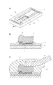
図1(a)は、本発明の液体吐出ヘッドを構成する記録素子基板の一例である。記録素子基板は、基板1と、液体を吐出するエネルギーを発生するエネルギー発生素子15とを有する。基板1は、シリコン等で形成されている。基板1にはエネルギー発生素子15に液体を供給する供給口11が形成されている。供給口は、基板にレーザーを照射したり、TMAH等によって異方性エッチングをしたり、ドライエッチングを行ったりすることで形成する。基板上には、供給口から供給された液体を吐出する吐出口13を形成する吐出口形成部材12が設けられている。吐出口形成部材は、例えば樹脂(特には感光性樹脂)や無機膜等で形成する。
FIG. 1A is an example of a recording element substrate constituting the liquid ejection head of the present invention. The recording element substrate includes a
エネルギー発生素子15は、TaSiN等で形成された熱エネルギーを発生する素子であってもよいし、圧電素子であってもよい。また、エネルギー発生素子は、基板上に直接形成されていても、基板に対して中空状に形成されていてもよい。エネルギー発生素子への電気の供給は、記録素子基板が有する電極パッド(不図示)と電極パッド上に形成されたバンプ7とを用い、外部の電気配線基板から電気を供給することで行われる。電気配線基板からの電気の供給は、バンプ7と電気配線基板とを配線によって接続することで行う。
The
図1(b)は、図1(a)のA−Aにおける断面図であり、バンプ7周辺を拡大した図である。バンプ周辺では、基板1上にSiO2等で形成された絶縁層2があり、その上にアルミニウム等で形成された電極パッド3がある。電極パッド3は、P−SiN等で形成された保護層4に挟まれている。電極パッド3上には、拡散防止層5が形成されており、その上にめっきで形成されたバンプ7が形成されている。バンプ7は、第一面18と第二面19とを有する。第一面及び第二面は、基板の表面に実質的に平行である。第二面は、第一面よりも基板の表面からの高さが高い。第一面には突起8が形成されている。第二面ではバンプとインナーリード等の配線とが接続されており、記録素子基板と電気配線基板とが配線を介して電気的に接続する。図1(c)に、バンプの第二面においてバンプと配線9とが接続されている様子を示す。接続部分の周囲は、封止材10で封止されていることが好ましい。また、図1(c)においては、電極パッドの表面の、バンプの第一面の突起に対応した位置に、突起が形成されている。
FIG. 1B is a cross-sectional view taken along the line AA of FIG. 1A, and is an enlarged view of the periphery of the
本発明の液体吐出ヘッドは、このような構成なので、突起8と配線9との接触を容易に避けることができる。突起8の上面の位置を配線9よりも下側にすることで、バンプと配線を接触させても突起と配線とは接触しない。即ち、第二面と第一面との高さの差は、突起の高さよりも大きい。この場合、配線による圧力が突起を通して基板に伝わることはない。或いは、突起8の上面が配線9と僅かに接触する程度であっても、配線による圧力は突起を通しては基板に僅かしか伝わらない。
Since the liquid ejection head according to the present invention has such a configuration, contact between the
従って、本発明の構成によれば、上述したような基板へのクラック発生を抑制することができる。また、バンプの低い位置である第一面に突起が形成されているので、突起を避けて配線を配置することが非常に容易である。さらに言えば、バンプに形成された突起の上面の位置よりも高い位置或いは同じ高さの位置に、バンプと配線とが接続された面があればよい。また、本発明の構成によれば、突起を低い位置に形成することから、突起を配線の下に配置するようなレイアウトが可能となり、電極パッドやバンプの面積を大きくしなくてもよい。よって、1枚のウェハから得られる記録素子基板の数をこれらの理由で減らさなくて済む。 Therefore, according to the configuration of the present invention, the occurrence of cracks in the substrate as described above can be suppressed. Further, since the protrusion is formed on the first surface where the bump is low, it is very easy to arrange the wiring while avoiding the protrusion. In other words, it is only necessary to have a surface where the bump and the wiring are connected at a position higher than or equal to the position of the upper surface of the protrusion formed on the bump. Further, according to the configuration of the present invention, since the protrusion is formed at a low position, a layout in which the protrusion is disposed under the wiring becomes possible, and the area of the electrode pad and the bump need not be increased. Therefore, it is not necessary to reduce the number of recording element substrates obtained from one wafer for these reasons.
次に、本発明の液体吐出ヘッドの製造方法を、図4を用いて説明する。 Next, the manufacturing method of the liquid discharge head of the present invention will be described with reference to FIG.
まず、シリコン等で形成された基板1を用意する。基板1は、SiO2等で形成された絶縁層2を表面に有する。絶縁層2上には、アルミニウム等で形成された電極パッド3と、電極パッド3を囲むP−SiN等で形成された保護層4とがある。これらは、例えば真空成膜法で形成する。スルーホール14は、フォトリソグラフィー技術等により保護層4のパターニングを行って形成する。次に、スルーホールに露出した電極パッド3に対し、プローブピン20が並んだブロープカードを、電極パッドの表面に自然に形成された自然酸化膜を破るようにして電極パッドに突き刺し、電気を流して電気抵抗等を測定し、エネルギー発生素子の電気的接続を確認する。プローブピン20は、針状の構造物である。これにより、図4(a)に示すように、電極パッド3の表面には、電極パッドが削られた部分(凹部)と、削られた分だけ電極パッドが盛り上がる突起(電気検査痕)ができる。尚、電極パッド上にバンプを形成してからバンプに電気検査を行うことも可能であるが、バンプを形成してしまう前に電気検査を行った方が製造効率を高めることができるため好ましい。突起はバンプの中心よりも外側(電気配線基板と記録素子基板との配線が延びる側、図4では右側)に形成する方が好ましい。中心よりも外側に形成することで、配線と突起との接触をより抑制することができる。
First, a
次に、図4(b)に示すように、電極パッド3の表面に、真空成膜装置等を用いて拡散防止層5を形成する。拡散防止層5としては、例えば高融点金属材料であるチタンタングステン等を用いる。拡散防止層は、電極パッドの表面形状に倣って形成され、拡散防止層にも凹部や突起が形成される。
Next, as shown in FIG. 4B, the
次に、図4(c)に示すように、電解めっきプロセスで電流を受けるカソード電極の役割と、めっき成長の核としての役割とを有するシード層6を成膜する。シード層としては、例えば金を0.03〜0.07μmの膜厚で全面成膜して形成する。シード層も、電極パッドの表面形状に倣って形成される。即ち、シード層にも凹部や突起が形成される。
Next, as shown in FIG. 4C, a
次に、図4(d)に示すように、レジスト17をスピンコート法などで基板全面に塗布する。レジストは、バンプの配線が接続される面(第二面)の高さよりも高くなるように形成する。レジストとしては、例えば感光性樹脂を用いることができる。 Next, as shown in FIG. 4D, a resist 17 is applied to the entire surface of the substrate by spin coating or the like. The resist is formed to be higher than the height of the surface (second surface) to which the bump wiring is connected. As the resist, for example, a photosensitive resin can be used.
次に、図4(e)に示すように、レジスト17にフォトリソグラフィー法によって第一の露光、現像を行い、めっき成長によってバンプ7が形成される部位のシード層6を露出させる。
Next, as shown in FIG. 4E, first exposure and development are performed on the resist 17 by a photolithography method to expose the
次に、図4(f)に示すように、電解めっき法により、亜硫酸金塩のめっき液中でシード層6に所定の電流を流し、レジスト17で覆われていない領域に金等のめっきを析出させ、バンプの一部を形成する。例えばこの部分のバンプの厚みを4μmとする場合、めっき時間は10.5分とする。ここで形成したバンプは、配線接続領域の一部となる。
Next, as shown in FIG. 4 (f), a predetermined current is passed through the
次に、図4(g)に示すように、レジスト17にフォトリソグラフィー法によって第二の露光、現像を行い、突起が形成された突起形成領域上のシード層6を露出させる。
Next, as shown in FIG. 4G, the resist 17 is subjected to second exposure and development by a photolithography method to expose the
次に、図4(h)に示すように、電解めっき法によりめっきを成長させる。めっきは、突起が形成されたシード層6がめっきによって覆われる程度に行えばよい。このめっきを行うと、先に成長させためっき部分も同様に成長する。突起が形成された領域にもめっきを成長させる理由は、次の通りである。即ち、次工程でシード層6を除去する際に、アルミニウム等で形成した電極パッドが露出すると、めっき(金)とアルミニウムの異種金属間で発生する電池反応で、電極パッドが腐食し、電極パッド上のバンプ7自体が剥がれてしまう。このため、めっきを保護膜として機能させることで、バンプ7の剥がれを抑制することができる。この工程により、バンプの配線接続領域と突起形成領域とが完成する。配線接続領域とは、先のめっきで形成した領域を含み、バンプの第二面を有する領域である。突起形成領域とは、2回目のめっきで形成した電極パッドの突起上の領域で、バンプの第一面を有する領域である。このように、バンプの第一面の突起は、電極パッドの表面の突起に対応した位置に形成される。逆に言えば、電極パッドの表面の、バンプの第一面の突起に対応した位置に、突起が形成された状態となる。
Next, as shown in FIG. 4H, plating is grown by an electrolytic plating method. The plating may be performed to such an extent that the
次に、図4(i)に示すように、レジスト17を溶剤等で除去する。続いて、図4(j)に示すように、形成したバンプ7をマスクとしてシード層6を除去する。シード層を除去する液としては、例えば窒素系有機化合物とヨウ素ヨウ化カリウムを含む液を用いる。シード層6を除去することで、拡散防止層5が露出する。シード層が0.03〜0.07μmの膜厚である場合、エッチング液に浸漬させてシード層を除去しても、突起形成領域のバンプ(めっき)は0.95μm程度の厚みで残る。従って、アルミニウムの腐食は抑制される。
Next, as shown in FIG. 4I, the resist 17 is removed with a solvent or the like. Subsequently, as shown in FIG. 4J, the
次に、図4(k)に示すように、記録素子基板をH2O2等のエッチング液に浸漬させ、バンプ7をマスクとして用いて不要となった拡散防止層5を除去する。これにより、全面に形成された拡散防止層によって同電位になっていた記録素子基板が有する各電極パッド及びバンプを分離する。
Next, as shown in FIG. 4 (k), the recording element substrate is immersed in an etchant such as H 2 O 2 and the
続いて、バンプ7に加熱処理であるアニール処理を行う。アニール処理を行うことで、配線を接続するバンプの硬度を70Hv以下とすることが好ましい。硬度が70Hv以下であると、配線を良好に接続することができる。即ち、バンプの第二面となる配線接続領域のバンプの硬度を70Hv以下とすることが好ましい。
Subsequently, the
また、2回目のめっきによってバンプを形成した場合、配線接続領域のバンプと突起形成領域のバンプとは硬度が異なってしまい、バンプの信頼性が低下することがある。例えば、金めっき形成時に基板とめっき液に与える電流密度を約0.6A/dm2に設定にすると、形成されたバンプの硬度は120Hv程度となる。一方、電流密度を約1.2A/dm2に設定すると、形成されたバンプの硬度は145Hv程度となる。このように硬度が異なった2種類の部位によってバンプが形成されていると、バンプの信頼性が低下する。そこで、アニール処理を行うのが好ましい。但し、この例において100℃1時間のアニール処理を行った場合、電流密度を約1.2A/dm2に設定して形成したバンプの硬度は50Hv程度まで急激に低下する。一方で、電流密度を約0.6A/dm2に設定して形成したバンプの硬度は120Hv程度からほとんど変化しない。このように、単にアニール処理を行うだけでは、硬度の差が大きいままとなってしまう場合がある。この例においては、さらに150℃1時間のアニール処理を行うと、それぞれ50Hv程度の硬度で安定する。即ち、本発明においては、1つのバンプのうち、配線接続領域のバンプと突起形成領域のバンプとの硬度の差を10Hv以下とするようにアニール処理を行うことが好ましい。硬度の差はなければない方がよいので、0Hv以上であることが好ましい。さらには、硬度をともに70Hv以下となるようにアニール処理を行うことが好ましい。また、アニール処理によって配線接続領域と突起形成領域との界面では再結晶化が起こり結合する。そして、界面に存在する不純物を除去することができる。このような理由からも、アニール処理を行うことが好ましい。 In addition, when bumps are formed by the second plating, the bumps in the wiring connection region and the bumps in the projection formation region have different hardness, which may reduce the reliability of the bumps. For example, if the current density applied to the substrate and the plating solution during gold plating is set to about 0.6 A / dm 2 , the hardness of the formed bump is about 120 Hv. On the other hand, when the current density is set to about 1.2 A / dm 2 , the hardness of the formed bump is about 145 Hv. When the bump is formed by two kinds of portions having different hardnesses as described above, the reliability of the bump is lowered. Therefore, it is preferable to perform an annealing process. However, in this example, when annealing is performed at 100 ° C. for 1 hour, the hardness of the bump formed with the current density set to about 1.2 A / dm 2 rapidly decreases to about 50 Hv. On the other hand, the hardness of the bump formed by setting the current density to about 0.6 A / dm 2 hardly changes from about 120 Hv. As described above, simply performing the annealing treatment may cause a large difference in hardness. In this example, further annealing at 150 ° C. for 1 hour stabilizes each with a hardness of about 50 Hv. That is, in the present invention, it is preferable to perform the annealing process so that the difference in hardness between the bumps in the wiring connection region and the bumps in the protrusion formation region is 10 Hv or less. Since it is better that there is no difference in hardness, it is preferably 0 Hv or more. Furthermore, it is preferable to perform the annealing process so that both the hardnesses are 70 Hv or less. In addition, recrystallization occurs and bonds at the interface between the wiring connection region and the protrusion formation region due to the annealing treatment. Then, impurities present at the interface can be removed. For this reason, it is preferable to perform an annealing process.
アニール処理は、上記硬度になるように行うのが好ましく、例えば200〜300℃で30分〜120分のアニール処理とすることが好ましい。液体吐出ヘッドにおいては後の工程で吐出口形成部材等をベークするプロセスを有する場合が多い。従って、そのプロセスにおいて不純物が発生しないようにするため、吐出口形成部材等をベークするプロセスの加熱温度よりも高い温度でアニール処理を行うことが好ましい。 The annealing treatment is preferably performed so as to have the above-mentioned hardness. For example, it is preferable to perform the annealing treatment at 200 to 300 ° C. for 30 to 120 minutes. In many cases, the liquid discharge head includes a process of baking the discharge port forming member and the like in a later step. Therefore, in order to prevent impurities from being generated in the process, it is preferable to perform the annealing process at a temperature higher than the heating temperature of the process of baking the discharge port forming member and the like.
最後に、配線9をバンプ7の第二面に接続させて、記録素子基板と電気配線基板、特には記録素子基板のエネルギー発生素子15と電気配線基板とが、配線9を介して電気的に接続する。
Finally, the wiring 9 is connected to the second surface of the
尚、図4(e)の段階で、レジスト17を、配線接続領域と突起形成領域とを一気に露出させるように開口させてもよい。この場合、次に1回目で1μm程度の厚みでめっきを形成し、レジスト除去後、再度レジスト塗布、露光、現像し、配線接続領域に追加めっきを行う。この手法でも本発明の液体吐出ヘッドを製造することができる。但し、レジストを複数回使用する必要がある。また、2回目の露光時にプロキシミティータイプの露光機を使用すると、露光時のアライメントが難しい。 Note that, at the stage of FIG. 4E, the resist 17 may be opened so that the wiring connection region and the protrusion formation region are exposed at once. In this case, plating is then formed with a thickness of about 1 μm for the first time, and after resist removal, resist coating, exposure, and development are performed again, and additional plating is performed on the wiring connection region. Even with this method, the liquid discharge head of the present invention can be manufactured. However, it is necessary to use the resist multiple times. If a proximity type exposure machine is used during the second exposure, alignment during exposure is difficult.
以上のようにして、本発明の液体吐出ヘッドを製造することができる。 As described above, the liquid discharge head of the present invention can be manufactured.
Claims (17)
前記バンプは、前記基板とは反対側の面に、前記基板の表面と実質的に平行な、第一面と、前記第一面よりも前記基板の表面からの高さが高い第二面と、を有し、
前記第一面には突起が形成されており、前記第二面において前記バンプと前記配線とが接続されていることを特徴とする液体吐出ヘッド。 A recording element substrate comprising: a substrate; an energy generating element that generates energy for discharging liquid; an electrode pad electrically connected to the energy generating element; and a bump formed on the electrode pad; A liquid ejection head having an electrical wiring substrate electrically connected by a bump and wiring of the element substrate,
The bump has a first surface substantially parallel to the surface of the substrate on a surface opposite to the substrate, and a second surface having a height higher from the surface of the substrate than the first surface. Have
A protrusion is formed on the first surface, and the bump and the wiring are connected on the second surface.
表面に突起が形成された電極パッドと、エネルギー発生素子とを有する基板を用意する工程と、
前記電極パッドの表面に突起が形成されていない部分の一部を露出するように、前記電極パッド上にレジストを形成する工程と、
前記露出した電極パッドの表面からめっきを行い、バンプの一部を形成する工程と、
前記電極パッドの表面に突起が形成された部分を露出するように、前記レジストの一部を除去する工程と、
前記バンプの一部と、前記レジストの一部を除去して露出した電極パッドの表面からめっきを行い、前記バンプの一部からめっきを行った部分を第二面を有する配線接続領域とし、前記レジストの一部を除去して露出した電極パッドの表面からめっきを行った部分を第一面を有する突起形成領域とする工程と、
前記第二面において前記バンプと前記配線とを接続する工程と、を有し
前記第二面は前記第一面よりも前記基板の表面からの高さが高いことを特徴とする液体吐出ヘッドの製造方法。 A recording element substrate comprising: a substrate; an energy generating element that generates energy for discharging liquid; an electrode pad electrically connected to the energy generating element; and a bump formed on the electrode pad; A method of manufacturing a liquid ejection head having an electrical wiring board electrically connected by a bump and wiring of an element substrate,
Preparing a substrate having electrode pads with protrusions formed on the surface and an energy generating element;
Forming a resist on the electrode pad so as to expose a part of a portion where no protrusion is formed on the surface of the electrode pad;
Plating from the exposed surface of the electrode pad to form part of the bump;
Removing a part of the resist so as to expose a portion where a protrusion is formed on the surface of the electrode pad;
Plating from a part of the bump and the surface of the electrode pad exposed by removing a part of the resist, a part plated from the part of the bump as a wiring connection region having a second surface, Removing a part of the resist and forming a protrusion-formed region having a first surface by plating from the exposed electrode pad surface;
A step of connecting the bump and the wiring on the second surface, wherein the second surface is higher in height from the surface of the substrate than the first surface. Production method.
Priority Applications (2)
| Application Number | Priority Date | Filing Date | Title |
|---|---|---|---|
| JP2012173756A JP6066612B2 (en) | 2012-08-06 | 2012-08-06 | Liquid discharge head and manufacturing method thereof |
| US13/956,737 US9174439B2 (en) | 2012-08-06 | 2013-08-01 | Liquid ejection head and method for manufacturing liquid ejection head |
Applications Claiming Priority (1)
| Application Number | Priority Date | Filing Date | Title |
|---|---|---|---|
| JP2012173756A JP6066612B2 (en) | 2012-08-06 | 2012-08-06 | Liquid discharge head and manufacturing method thereof |
Publications (3)
| Publication Number | Publication Date |
|---|---|
| JP2014030980A JP2014030980A (en) | 2014-02-20 |
| JP2014030980A5 JP2014030980A5 (en) | 2015-09-10 |
| JP6066612B2 true JP6066612B2 (en) | 2017-01-25 |
Family
ID=50025075
Family Applications (1)
| Application Number | Title | Priority Date | Filing Date |
|---|---|---|---|
| JP2012173756A Active JP6066612B2 (en) | 2012-08-06 | 2012-08-06 | Liquid discharge head and manufacturing method thereof |
Country Status (2)
| Country | Link |
|---|---|
| US (1) | US9174439B2 (en) |
| JP (1) | JP6066612B2 (en) |
Families Citing this family (2)
| Publication number | Priority date | Publication date | Assignee | Title |
|---|---|---|---|---|
| JP2016141149A (en) * | 2015-02-05 | 2016-08-08 | キヤノン株式会社 | Manufacturing method for substrate for liquid discharge head and substrate for liquid discharge head manufactured by the manufacturing method |
| TWI645586B (en) * | 2017-12-05 | 2018-12-21 | 國家中山科學研究院 | Method of preparing secondary lens with hollow nano-structure for uniform illuminance |
Family Cites Families (15)
| Publication number | Priority date | Publication date | Assignee | Title |
|---|---|---|---|---|
| JPH0797587B2 (en) * | 1987-03-12 | 1995-10-18 | 株式会社東芝 | Method for manufacturing semiconductor device |
| JP2653179B2 (en) * | 1989-08-21 | 1997-09-10 | 富士電機株式会社 | Method of manufacturing bump electrode for integrated circuit device |
| US20020053734A1 (en) * | 1993-11-16 | 2002-05-09 | Formfactor, Inc. | Probe card assembly and kit, and methods of making same |
| JP3584509B2 (en) * | 1994-12-27 | 2004-11-04 | 松下電器産業株式会社 | Ink jet printer head and method of manufacturing the same |
| US6833613B1 (en) * | 1997-12-18 | 2004-12-21 | Micron Technology, Inc. | Stacked semiconductor package having laser machined contacts |
| US6426556B1 (en) * | 2001-01-16 | 2002-07-30 | Megic Corporation | Reliable metal bumps on top of I/O pads with test probe marks |
| JP4630680B2 (en) * | 2005-01-31 | 2011-02-09 | キヤノン株式会社 | Manufacturing method of semiconductor element and manufacturing method of ink jet recording head |
| CN100555589C (en) * | 2005-06-29 | 2009-10-28 | 皇家飞利浦电子股份有限公司 | Make the method for semiconductor subassembly |
| US8438729B2 (en) * | 2006-03-09 | 2013-05-14 | Canon Kabushiki Kaisha | Method of producing liquid discharge head |
| JP4822353B2 (en) * | 2006-03-09 | 2011-11-24 | キヤノン株式会社 | Liquid discharge head and manufacturing method thereof |
| JP2007307833A (en) | 2006-05-19 | 2007-11-29 | Canon Inc | Inkjet recording head |
| JP5168443B2 (en) * | 2006-08-08 | 2013-03-21 | セイコーエプソン株式会社 | Piezoelectric element, actuator device, liquid jet head, and liquid jet device |
| JP2008153470A (en) * | 2006-12-18 | 2008-07-03 | Renesas Technology Corp | Semiconductor apparatus and manufacturing method of semiconductor apparatus |
| JP5379527B2 (en) * | 2009-03-19 | 2013-12-25 | パナソニック株式会社 | Semiconductor device |
| US8581420B2 (en) * | 2010-10-18 | 2013-11-12 | Taiwan Semiconductor Manufacturing Company, Ltd. | Under-bump metallization (UBM) structure and method of forming the same |
-
2012
- 2012-08-06 JP JP2012173756A patent/JP6066612B2/en active Active
-
2013
- 2013-08-01 US US13/956,737 patent/US9174439B2/en not_active Expired - Fee Related
Also Published As
| Publication number | Publication date |
|---|---|
| US9174439B2 (en) | 2015-11-03 |
| JP2014030980A (en) | 2014-02-20 |
| US20140035999A1 (en) | 2014-02-06 |
Similar Documents
| Publication | Publication Date | Title |
|---|---|---|
| US9392705B2 (en) | Wiring board with through wiring | |
| EP3806141A1 (en) | Method of manufacturing glass device and glass device | |
| TWI566351B (en) | Semiconductor apparatus and method for fabricating the same | |
| JP5107187B2 (en) | Manufacturing method of electronic component package | |
| JPH08250498A (en) | Semiconductor device and its manufacture | |
| JP2015041773A (en) | Interposer substrate and method of manufacturing the same | |
| JP5276895B2 (en) | Probe card and manufacturing method thereof | |
| KR101708535B1 (en) | Integrated circuit apparatus and method for manufacturing the same | |
| JP6066612B2 (en) | Liquid discharge head and manufacturing method thereof | |
| CN107567651B (en) | Wiring substrate having through electrode and method for manufacturing the same | |
| US7563703B2 (en) | Microelectronic interconnect device comprising localised conductive pins | |
| JP2023081264A (en) | Multilayer wiring board manufacturing method | |
| JP2017212271A (en) | Wiring board, manufacturing method of the same, and electronic component device | |
| JP2008153275A (en) | Semiconductor substrate and its manufacturing method | |
| JP2011082531A (en) | Through-hole electrode substrate, and method of manufacturing the same | |
| JP2016141149A (en) | Manufacturing method for substrate for liquid discharge head and substrate for liquid discharge head manufactured by the manufacturing method | |
| US8108993B2 (en) | Method of manufacturing wiring substrate, and method of manufacturing semiconductor device | |
| JP2009094230A (en) | Semiconductor device and manufacturing method thereof | |
| JP2008241595A (en) | Substrate for probe card assembly and probe card using it | |
| JP5596962B2 (en) | Method for manufacturing substrate for liquid discharge head and method for manufacturing liquid discharge head | |
| JP2010221656A (en) | Board for liquid discharging head | |
| JP2013207067A (en) | Semiconductor device and manufacturing method of the same | |
| KR100743978B1 (en) | Contact element for probe card and method for producing the same | |
| JP2011238742A (en) | Method for manufacturing a wiring substrate and the wiring substrate | |
| JP2017126865A (en) | Method of manufacturing electronic component, and the electronic component |
Legal Events
| Date | Code | Title | Description |
|---|---|---|---|
| A521 | Request for written amendment filed |
Free format text: JAPANESE INTERMEDIATE CODE: A523 Effective date: 20150727 |
|
| A621 | Written request for application examination |
Free format text: JAPANESE INTERMEDIATE CODE: A621 Effective date: 20150727 |
|
| A977 | Report on retrieval |
Free format text: JAPANESE INTERMEDIATE CODE: A971007 Effective date: 20160511 |
|
| A131 | Notification of reasons for refusal |
Free format text: JAPANESE INTERMEDIATE CODE: A131 Effective date: 20160524 |
|
| A521 | Request for written amendment filed |
Free format text: JAPANESE INTERMEDIATE CODE: A523 Effective date: 20160720 |
|
| TRDD | Decision of grant or rejection written | ||
| A01 | Written decision to grant a patent or to grant a registration (utility model) |
Free format text: JAPANESE INTERMEDIATE CODE: A01 Effective date: 20161122 |
|
| A61 | First payment of annual fees (during grant procedure) |
Free format text: JAPANESE INTERMEDIATE CODE: A61 Effective date: 20161220 |
|
| R151 | Written notification of patent or utility model registration |
Ref document number: 6066612 Country of ref document: JP Free format text: JAPANESE INTERMEDIATE CODE: R151 |