JP6043548B2 - Capacitor - Google Patents
Capacitor Download PDFInfo
- Publication number
- JP6043548B2 JP6043548B2 JP2012191162A JP2012191162A JP6043548B2 JP 6043548 B2 JP6043548 B2 JP 6043548B2 JP 2012191162 A JP2012191162 A JP 2012191162A JP 2012191162 A JP2012191162 A JP 2012191162A JP 6043548 B2 JP6043548 B2 JP 6043548B2
- Authority
- JP
- Japan
- Prior art keywords
- hole
- hole diameter
- capacitor
- internal electrode
- diameter portion
- Prior art date
- Legal status (The legal status is an assumption and is not a legal conclusion. Google has not performed a legal analysis and makes no representation as to the accuracy of the status listed.)
- Active
Links
- 239000003990 capacitor Substances 0.000 title claims description 88
- 239000000463 material Substances 0.000 claims description 27
- 230000009471 action Effects 0.000 claims description 5
- TWNQGVIAIRXVLR-UHFFFAOYSA-N oxo(oxoalumanyloxy)alumane Chemical compound O=[Al]O[Al]=O TWNQGVIAIRXVLR-UHFFFAOYSA-N 0.000 claims description 5
- 238000007743 anodising Methods 0.000 claims description 3
- 239000004020 conductor Substances 0.000 description 67
- 230000015556 catabolic process Effects 0.000 description 19
- 238000004519 manufacturing process Methods 0.000 description 17
- 238000009413 insulation Methods 0.000 description 12
- 230000007423 decrease Effects 0.000 description 8
- 238000010586 diagram Methods 0.000 description 8
- 239000003989 dielectric material Substances 0.000 description 8
- 239000012212 insulator Substances 0.000 description 7
- 238000000034 method Methods 0.000 description 7
- 230000004048 modification Effects 0.000 description 7
- 238000012986 modification Methods 0.000 description 7
- 230000003647 oxidation Effects 0.000 description 7
- 238000007254 oxidation reaction Methods 0.000 description 7
- 239000000758 substrate Substances 0.000 description 7
- 230000005684 electric field Effects 0.000 description 6
- 229910052751 metal Inorganic materials 0.000 description 6
- 239000002184 metal Substances 0.000 description 6
- 238000009713 electroplating Methods 0.000 description 5
- 229910044991 metal oxide Inorganic materials 0.000 description 5
- 150000004706 metal oxides Chemical class 0.000 description 5
- 230000015572 biosynthetic process Effects 0.000 description 4
- 230000006872 improvement Effects 0.000 description 4
- 238000012423 maintenance Methods 0.000 description 4
- MUBZPKHOEPUJKR-UHFFFAOYSA-N Oxalic acid Chemical compound OC(=O)C(O)=O MUBZPKHOEPUJKR-UHFFFAOYSA-N 0.000 description 3
- 239000000956 alloy Substances 0.000 description 3
- 229910045601 alloy Inorganic materials 0.000 description 3
- 229910052782 aluminium Inorganic materials 0.000 description 3
- 229910052804 chromium Inorganic materials 0.000 description 3
- 239000012141 concentrate Substances 0.000 description 3
- 229910052802 copper Inorganic materials 0.000 description 3
- 229910052742 iron Inorganic materials 0.000 description 3
- 229910052745 lead Inorganic materials 0.000 description 3
- 229910052759 nickel Inorganic materials 0.000 description 3
- 229910052763 palladium Inorganic materials 0.000 description 3
- 238000001020 plasma etching Methods 0.000 description 3
- 229910052697 platinum Inorganic materials 0.000 description 3
- 239000011148 porous material Substances 0.000 description 3
- 229910052709 silver Inorganic materials 0.000 description 3
- 238000004544 sputter deposition Methods 0.000 description 3
- 229910052718 tin Inorganic materials 0.000 description 3
- 238000001771 vacuum deposition Methods 0.000 description 3
- 229910018072 Al 2 O 3 Inorganic materials 0.000 description 2
- 239000004593 Epoxy Substances 0.000 description 2
- 239000004642 Polyimide Substances 0.000 description 2
- NIXOWILDQLNWCW-UHFFFAOYSA-N acrylic acid group Chemical group C(C=C)(=O)O NIXOWILDQLNWCW-UHFFFAOYSA-N 0.000 description 2
- 238000009835 boiling Methods 0.000 description 2
- 239000000470 constituent Substances 0.000 description 2
- 229910052737 gold Inorganic materials 0.000 description 2
- 229920001721 polyimide Polymers 0.000 description 2
- 230000008569 process Effects 0.000 description 2
- 239000011347 resin Substances 0.000 description 2
- 229920005989 resin Polymers 0.000 description 2
- 229910052719 titanium Inorganic materials 0.000 description 2
- XLYOFNOQVPJJNP-UHFFFAOYSA-N water Chemical compound O XLYOFNOQVPJJNP-UHFFFAOYSA-N 0.000 description 2
- 238000001039 wet etching Methods 0.000 description 2
- AZDRQVAHHNSJOQ-UHFFFAOYSA-N alumane Chemical group [AlH3] AZDRQVAHHNSJOQ-UHFFFAOYSA-N 0.000 description 1
- XAGFODPZIPBFFR-UHFFFAOYSA-N aluminium Chemical compound [Al] XAGFODPZIPBFFR-UHFFFAOYSA-N 0.000 description 1
- 229910052787 antimony Inorganic materials 0.000 description 1
- 238000006243 chemical reaction Methods 0.000 description 1
- 238000001312 dry etching Methods 0.000 description 1
- 230000000694 effects Effects 0.000 description 1
- 229910052735 hafnium Inorganic materials 0.000 description 1
- 239000011810 insulating material Substances 0.000 description 1
- 229910052741 iridium Inorganic materials 0.000 description 1
- 230000001788 irregular Effects 0.000 description 1
- 229910052758 niobium Inorganic materials 0.000 description 1
- 235000006408 oxalic acid Nutrition 0.000 description 1
- 238000007747 plating Methods 0.000 description 1
- 238000005498 polishing Methods 0.000 description 1
- 238000003825 pressing Methods 0.000 description 1
- 229910052703 rhodium Inorganic materials 0.000 description 1
- 229910052707 ruthenium Inorganic materials 0.000 description 1
- 238000000992 sputter etching Methods 0.000 description 1
- 239000000126 substance Substances 0.000 description 1
- 229910052715 tantalum Inorganic materials 0.000 description 1
- 230000007704 transition Effects 0.000 description 1
- 229910052721 tungsten Inorganic materials 0.000 description 1
- 229910052725 zinc Inorganic materials 0.000 description 1
- 229910052726 zirconium Inorganic materials 0.000 description 1
Images


Classifications
-
- H—ELECTRICITY
- H01—ELECTRIC ELEMENTS
- H01G—CAPACITORS; CAPACITORS, RECTIFIERS, DETECTORS, SWITCHING DEVICES, LIGHT-SENSITIVE OR TEMPERATURE-SENSITIVE DEVICES OF THE ELECTROLYTIC TYPE
- H01G4/00—Fixed capacitors; Processes of their manufacture
- H01G4/33—Thin- or thick-film capacitors
-
- H—ELECTRICITY
- H01—ELECTRIC ELEMENTS
- H01G—CAPACITORS; CAPACITORS, RECTIFIERS, DETECTORS, SWITCHING DEVICES, LIGHT-SENSITIVE OR TEMPERATURE-SENSITIVE DEVICES OF THE ELECTROLYTIC TYPE
- H01G4/00—Fixed capacitors; Processes of their manufacture
- H01G4/002—Details
- H01G4/005—Electrodes
- H01G4/012—Form of non-self-supporting electrodes
-
- H—ELECTRICITY
- H01—ELECTRIC ELEMENTS
- H01G—CAPACITORS; CAPACITORS, RECTIFIERS, DETECTORS, SWITCHING DEVICES, LIGHT-SENSITIVE OR TEMPERATURE-SENSITIVE DEVICES OF THE ELECTROLYTIC TYPE
- H01G4/00—Fixed capacitors; Processes of their manufacture
- H01G4/30—Stacked capacitors
-
- H—ELECTRICITY
- H01—ELECTRIC ELEMENTS
- H01G—CAPACITORS; CAPACITORS, RECTIFIERS, DETECTORS, SWITCHING DEVICES, LIGHT-SENSITIVE OR TEMPERATURE-SENSITIVE DEVICES OF THE ELECTROLYTIC TYPE
- H01G4/00—Fixed capacitors; Processes of their manufacture
- H01G4/002—Details
- H01G4/018—Dielectrics
- H01G4/06—Solid dielectrics
- H01G4/08—Inorganic dielectrics
- H01G4/10—Metal-oxide dielectrics
-
- H—ELECTRICITY
- H01—ELECTRIC ELEMENTS
- H01G—CAPACITORS; CAPACITORS, RECTIFIERS, DETECTORS, SWITCHING DEVICES, LIGHT-SENSITIVE OR TEMPERATURE-SENSITIVE DEVICES OF THE ELECTROLYTIC TYPE
- H01G4/00—Fixed capacitors; Processes of their manufacture
- H01G4/002—Details
- H01G4/224—Housing; Encapsulation
-
- H—ELECTRICITY
- H01—ELECTRIC ELEMENTS
- H01G—CAPACITORS; CAPACITORS, RECTIFIERS, DETECTORS, SWITCHING DEVICES, LIGHT-SENSITIVE OR TEMPERATURE-SENSITIVE DEVICES OF THE ELECTROLYTIC TYPE
- H01G4/00—Fixed capacitors; Processes of their manufacture
- H01G4/002—Details
- H01G4/228—Terminals
- H01G4/236—Terminals leading through the housing, i.e. lead-through
-
- H—ELECTRICITY
- H01—ELECTRIC ELEMENTS
- H01G—CAPACITORS; CAPACITORS, RECTIFIERS, DETECTORS, SWITCHING DEVICES, LIGHT-SENSITIVE OR TEMPERATURE-SENSITIVE DEVICES OF THE ELECTROLYTIC TYPE
- H01G4/00—Fixed capacitors; Processes of their manufacture
- H01G4/30—Stacked capacitors
- H01G4/302—Stacked capacitors obtained by injection of metal in cavities formed in a ceramic body
-
- H—ELECTRICITY
- H01—ELECTRIC ELEMENTS
- H01G—CAPACITORS; CAPACITORS, RECTIFIERS, DETECTORS, SWITCHING DEVICES, LIGHT-SENSITIVE OR TEMPERATURE-SENSITIVE DEVICES OF THE ELECTROLYTIC TYPE
- H01G9/00—Electrolytic capacitors, rectifiers, detectors, switching devices, light-sensitive or temperature-sensitive devices; Processes of their manufacture
- H01G9/0029—Processes of manufacture
- H01G9/0032—Processes of manufacture formation of the dielectric layer
-
- H—ELECTRICITY
- H01—ELECTRIC ELEMENTS
- H01G—CAPACITORS; CAPACITORS, RECTIFIERS, DETECTORS, SWITCHING DEVICES, LIGHT-SENSITIVE OR TEMPERATURE-SENSITIVE DEVICES OF THE ELECTROLYTIC TYPE
- H01G9/00—Electrolytic capacitors, rectifiers, detectors, switching devices, light-sensitive or temperature-sensitive devices; Processes of their manufacture
- H01G9/004—Details
- H01G9/04—Electrodes or formation of dielectric layers thereon
- H01G9/048—Electrodes or formation of dielectric layers thereon characterised by their structure
-
- H—ELECTRICITY
- H01—ELECTRIC ELEMENTS
- H01G—CAPACITORS; CAPACITORS, RECTIFIERS, DETECTORS, SWITCHING DEVICES, LIGHT-SENSITIVE OR TEMPERATURE-SENSITIVE DEVICES OF THE ELECTROLYTIC TYPE
- H01G9/00—Electrolytic capacitors, rectifiers, detectors, switching devices, light-sensitive or temperature-sensitive devices; Processes of their manufacture
- H01G9/004—Details
- H01G9/07—Dielectric layers
Landscapes
- Engineering & Computer Science (AREA)
- Power Engineering (AREA)
- Microelectronics & Electronic Packaging (AREA)
- Manufacturing & Machinery (AREA)
- Chemical & Material Sciences (AREA)
- Ceramic Engineering (AREA)
- Inorganic Chemistry (AREA)
- Fixed Capacitors And Capacitor Manufacturing Machines (AREA)
Description
本発明は、ポーラスコンデンサに関する。 The present invention relates to a porous capacitor.
近年、新しいタイプのコンデンサとしてポーラスコンデンサが開発されている。ポーラスコンデンサは、アルミニウム等の金属表面に形成される金属酸化物がポーラス(細孔の貫通孔)構造を形成する性質を利用してポーラス内に内部電極を形成し、金属酸化物を誘電体としてコンデンサとしたものである。 In recent years, a porous capacitor has been developed as a new type of capacitor. Porous capacitors use a property that a metal oxide formed on a metal surface such as aluminum forms a porous (through-hole) structure, forms an internal electrode in the porous, and uses the metal oxide as a dielectric. It is a capacitor.
誘電体の表面及び裏面にはそれぞれ導電体が積層され、ポーラス内に形成される内部電極は表面の導電体と裏面の導電体のいずれか一方に接続される。内部電極と接続されない側の導電体の間は、空隙又は絶縁性材料によって絶縁される。これにより内部電極は、誘電体を介して対向する対向電極として機能する。 Conductors are stacked on the front and back surfaces of the dielectric, and the internal electrodes formed in the porous are connected to either the front or back conductors. The conductor on the side not connected to the internal electrode is insulated by a gap or an insulating material. As a result, the internal electrode functions as a counter electrode facing each other through the dielectric.
例えば、特許文献1及び特許文献2には、このような構成を有するポーラスコンデンサが開示されている。いずれの特許文献においても、ポーラス内に内部電極が形成され、内部電極の一端は一方の導電体に接続され、他端は他方の導電体と絶縁されている。
For example,
ここで、上記のような構成を有するポーラスコンデンサにおいては、対向する内部電極間の絶縁性能によってコンデンサの絶縁破壊耐圧が左右される。上述のように内部電極は誘電体のポーラス内に形成されているが、内部電極を隔てる誘電体層を厚くすれば、コンデンサの絶縁破壊耐圧を向上させることが可能である。しかしながら、内部電極を隔てる誘電体層を厚くすると、内部電極の対向距離が増大し、コンデンサとしての容量が減少する。即ち、ポーラスコンデンサの絶縁破壊耐圧の向上と容量の維持は共に実現することが困難である。 Here, in the porous capacitor having the above-described configuration, the dielectric breakdown voltage of the capacitor depends on the insulating performance between the opposing internal electrodes. As described above, the internal electrode is formed in the dielectric porous. However, if the dielectric layer separating the internal electrode is thickened, the dielectric breakdown voltage of the capacitor can be improved. However, when the dielectric layer separating the internal electrodes is thickened, the facing distance between the internal electrodes increases, and the capacitance as a capacitor decreases. That is, it is difficult to achieve both improvement of the dielectric breakdown voltage and maintenance of the capacitance of the porous capacitor.
以上のような事情に鑑み、本発明の目的は、絶縁破壊耐性の向上と容量の維持が共に可能なポーラスコンデンサを提供することにある。 In view of the circumstances as described above, an object of the present invention is to provide a porous capacitor capable of improving both breakdown resistance and maintaining capacity.
上記目的を達成するため、本発明の一形態に係るコンデンサは、誘電体層と、第1の外部電極層と、第2の外部電極層と、第1の内部電極と、第2の内部電極とを具備する。
上記誘電体層は、第1の面と、上記第1の面と反対側の第2の面と、上記第1の面と上記第2面に連通する複数の貫通孔とを備える誘電体層であって、上記複数の貫通孔は第1の貫通孔と第2の貫通孔とを含み、上記第1の貫通孔は第1の孔径を有する第1の孔径部と上記第2の面側において上記第1の孔径より小さい第2の孔径を有する第2の孔径部とを有する。
上記第1の外部電極層は、上記第1の面に配設されている。
上記第2の外部電極層は、上記第2の面に配設されている。
上記第1の内部電極は、上記第1の貫通孔内に形成され、上記第1の外部電極層に接続し、先端が前記第2の孔径部に位置して上記第2の外部電極層と離間する。
上記第2の内部電極は、上記第2の貫通孔内に形成され、上記第2の外部電極層に接続し、上記第1の外部電極層と離間する。
In order to achieve the above object, a capacitor according to one embodiment of the present invention includes a dielectric layer, a first external electrode layer, a second external electrode layer, a first internal electrode, and a second internal electrode. It comprises.
The dielectric layer includes a first surface, a second surface opposite to the first surface, and a plurality of through holes communicating with the first surface and the second surface. The plurality of through holes include a first through hole and a second through hole, and the first through hole has a first hole diameter portion having a first hole diameter and the second surface side. And a second hole diameter portion having a second hole diameter smaller than the first hole diameter.
The first external electrode layer is disposed on the first surface.
The second external electrode layer is disposed on the second surface.
The first internal electrode is formed in the first through-hole, is connected to the first external electrode layer, and a tip is located at the second hole diameter portion, and the second external electrode layer Separate.
The second internal electrode is formed in the second through hole, is connected to the second external electrode layer, and is separated from the first external electrode layer.
本発明の一実施形態に係るコンデンサは、誘電体層と、第1の外部電極層と、第2の外部電極層と、第1の内部電極と、第2の内部電極とを具備する。
上記誘電体層は、第1の面と、上記第1の面と反対側の第2の面と、上記第1の面と上記第2面に連通する複数の貫通孔とを備える誘電体層であって、上記複数の貫通孔は第1の貫通孔と第2の貫通孔とを含み、上記第1の貫通孔は第1の孔径を有する第1の孔径部と上記第2の面側において上記第1の孔径より小さい第2の孔径を有する第2の孔径部とを有する。
上記第1の外部電極層は、上記第1の面に配設されている。
上記第2の外部電極層は、上記第2の面に配設されている。
上記第1の内部電極は、上記第1の貫通孔内に形成され、上記第1の外部電極層に接続し、先端が上記第2の孔径部に位置して上記第2の外部電極層と離間する。
上記第2の内部電極は、上記第2の貫通孔内に形成され、上記第2の外部電極層に接続し、上記第1の外部電極層と離間する。
A capacitor according to an embodiment of the present invention includes a dielectric layer, a first external electrode layer, a second external electrode layer, a first internal electrode, and a second internal electrode.
The dielectric layer includes a first surface, a second surface opposite to the first surface, and a plurality of through holes communicating with the first surface and the second surface. The plurality of through holes include a first through hole and a second through hole, and the first through hole has a first hole diameter portion having a first hole diameter and the second surface side. And a second hole diameter portion having a second hole diameter smaller than the first hole diameter.
The first external electrode layer is disposed on the first surface.
The second external electrode layer is disposed on the second surface.
The first internal electrode is formed in the first through-hole, is connected to the first external electrode layer, and a tip is located in the second hole diameter portion and the second external electrode layer Separate.
The second internal electrode is formed in the second through hole, is connected to the second external electrode layer, and is separated from the first external electrode layer.
ポーラスコンデンサに電圧を印加していくと内部電極の先端部には電界が集中するため、内部電極の先端部が起点となって、対向する内部電極との間で絶縁耐圧が破壊する。上記の構成によれば、第1の貫通孔は小径となる第2の孔径部をもち、第1の内部電極の先端が第2の孔径部に位置するので、対向する内部電極に対して誘電体層の厚さが厚くなるため、絶縁性が良好となる。一方で、第1の貫通孔は第1の面側が大径であるため、第1の内部電極と対向する第2の内部電極の間の距離は小さく、コンデンサ容量の減少はそれほど生じない。このように、本実施形態に係るコンデンサにおいては、絶縁破壊耐圧の向上とコンデンサ容量の維持を同時に実現することが可能に構成されている。 When a voltage is applied to the porous capacitor, the electric field concentrates at the tip of the internal electrode, so that the withstand voltage is destroyed between the opposing internal electrodes starting from the tip of the internal electrode. According to the above configuration, the first through hole has the second hole diameter portion having a small diameter, and the tip of the first internal electrode is located at the second hole diameter portion. Since the thickness of the body layer is increased, the insulating property is improved. On the other hand, since the first through hole has a large diameter on the first surface side, the distance between the second internal electrode facing the first internal electrode is small, and the capacity of the capacitor does not decrease so much. As described above, the capacitor according to the present embodiment is configured to be capable of simultaneously improving the breakdown voltage and maintaining the capacitor capacity.
上記第2の貫通孔は、第3の孔径を有する第3の孔径部と、上記第1の面側において上記第3の孔径より小さい第4の孔径を有する第4の孔径部とを有し、
上記第2の内部電極は先端が上記第4の孔径部に位置してもよい。
The second through hole has a third hole diameter portion having a third hole diameter, and a fourth hole diameter portion having a fourth hole diameter smaller than the third hole diameter on the first surface side. ,
The tip of the second internal electrode may be located at the fourth hole diameter portion.
この構成によれば、第1の貫通孔と同様に、第2の貫通孔の孔径を均一とせず、第2の面側の孔径を第1の面側の孔径より大きくすることによって絶縁破壊耐圧の向上とコンデンサ容量の維持を同時に実現することが可能に構成されている。第2の貫通孔内に形成される第2の内部電極は、第2の外部電極層に接続され、第1の外部電極層と離間されるため、孔径の大小関係は、第1の貫通孔とは反対になっている。 According to this configuration, as in the case of the first through hole, the second through hole does not have a uniform hole diameter, and the second surface side has a larger hole diameter than the first surface side. Improvement and maintenance of the capacitor capacity can be realized at the same time. Since the second internal electrode formed in the second through hole is connected to the second external electrode layer and is separated from the first external electrode layer, the size relationship between the hole diameters is determined by the first through hole. Is the opposite.
上記第1の貫通孔は、上記第1の孔径部と上記第2の孔径部の間において、上記第1の孔径より小さく上記第2の孔径より大きい第5の孔径を有する第5の孔径部をさらに有し、
上記第2の貫通孔は、上記第3の孔径部と上記第4の孔径部の間において、上記第3の孔径より小さく上記第4の孔径より大きい第6の孔径を有する第6の孔径部をさらに有してもよい。
The first through hole has a fifth hole diameter portion having a fifth hole diameter smaller than the first hole diameter and larger than the second hole diameter between the first hole diameter portion and the second hole diameter portion. Further comprising
The second through hole is a sixth hole diameter portion having a sixth hole diameter smaller than the third hole diameter and larger than the fourth hole diameter between the third hole diameter portion and the fourth hole diameter portion. May further be included.
上述のように、第1の貫通孔は、内部に形成される第1の内部電極が絶縁される第2の外部電極層側が小径に形成されており、絶縁性が向上する。しかしながら、絶縁破壊の起点となる部位が第1内部電極の先端付近から段差コーナー部(孔径の段差)に移行して絶縁性が充分に向上しないことがある。ここで、第1の貫通孔に第1の孔径部と第2の孔径部の中間の孔径(第5の孔径)を有する第5の孔径部を設けることによって、段差コーナー部の電界集中を分散させ、該部を起点とした絶縁破壊を防止することが可能である。すなわち内部電極間の絶縁破壊耐圧をさらに向上させることができる。第2の貫通孔についても同様に、第6の孔径を有する第6の孔径部を設けることによって、第2の内部電極の段差コーナー部での絶縁破壊を防止することが可能である。即ち、上記構成によれば、コンデンサ容量を維持しつつ、絶縁破壊耐圧をさらに向上させることが可能である。加えて、第1の貫通孔及び第2の貫通孔はさらに多段階の孔径部を有するものとすることが可能であり、要求されるコンデンサ容量と絶縁破壊耐圧のバランスによって孔径の段数を決定することが可能である。 As described above, the first through-hole is formed with a small diameter on the second external electrode layer side where the first internal electrode formed therein is insulated, and the insulation is improved. However, the insulating breakdown may not be sufficiently improved due to the transition from the vicinity of the tip of the first internal electrode to the step corner (the step of the hole diameter). Here, by providing the first through hole with a fifth hole diameter portion having a hole diameter (fifth hole diameter) intermediate between the first hole diameter portion and the second hole diameter portion, the electric field concentration at the step corner portion is dispersed. Therefore, it is possible to prevent dielectric breakdown starting from the portion. That is, the breakdown voltage between the internal electrodes can be further improved. Similarly, for the second through hole, by providing a sixth hole diameter portion having a sixth hole diameter, it is possible to prevent dielectric breakdown at the step corner portion of the second internal electrode. That is, according to the above configuration, it is possible to further improve the breakdown voltage while maintaining the capacitor capacity. In addition, the first through hole and the second through hole can further have multi-stage hole diameter portions, and the number of hole diameters is determined by a balance between required capacitor capacity and dielectric breakdown voltage. It is possible.
上記誘電体層は、陽極酸化作用によって細孔を生じる材料からなるものであってもよい。 The dielectric layer may be made of a material that generates pores by anodic oxidation.
この構成によれば、当該材料の陽極酸化作用、すなわち自己組織化作用によって形成される細孔(ポーラス貫通孔)を、第1の貫通孔及び第2の貫通孔として利用することが可能である。 According to this configuration, the pores (porous through holes) formed by the anodic oxidation action, that is, the self-organizing action of the material can be used as the first through holes and the second through holes. .
上記誘電体層は、酸化アルミニウムからなるものであってもよい。 The dielectric layer may be made of aluminum oxide.
酸化アルミニウム(Al2O3)は、陽極酸化することによって自己組織化作用により細孔を生じ、かつ誘電性材料であるため、誘電体層の材料に好適である。 Aluminum oxide (Al 2 O 3 ) is suitable for the material of the dielectric layer because it is anodized to generate pores by a self-organizing action and is a dielectric material.
以下、図面を参照しながら、本発明の実施形態を説明する。 Hereinafter, embodiments of the present invention will be described with reference to the drawings.
(コンデンサの構成)
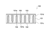
図1は本発明の一実施形態に係るコンデンサ100を示す斜視図であり、図2はコンデンサ100の断面図である。これらの図に示すように、コンデンサ100は、誘電体層101、第1外部電極層102、第2外部電極層103、第1内部電極104及び第2内部電極105を有する。
(Capacitor configuration)
FIG. 1 is a perspective view showing a
第1外部電極層102、誘電体層101及び第2外部電極層103はこの順で積層され、即ち誘電体層101は、第1外部電極層102及び第2外部電極層103によって挟まれている。第1内部電極104及び第2内部電極105は、図2に示すように誘電体層101に形成された貫通孔の内部に形成されている。なお、コンデンサ100には、ここに示す以外の構成、例えば、第1外部電極層102及び第2外部電極層103にそれぞれ接続された配線等が設けられていてもよい。
The first
誘電体層101は、コンデンサ100の誘電体として機能する層である。誘電体層101は、後述する貫通孔(ポーラス)を形成することが可能な誘電性材料からなるものとすることができ、特に陽極酸化されると自己組織化作用によってポーラスを生じる材料が好適である。このような材料としては、酸化アルミニウム(Al2O3)を挙げることができる。また、この他に誘電体層101は、弁金属(Al、Ta、Nb、Ti、Zr、Hf、Zn、W、Sb)の酸化物からなるものとすることが可能である。誘電体層101の厚みは特に限定されないが、例えば数μm〜数百μmとすることができる。
The
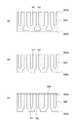
図3は、誘電体層101を示す斜視図である。同図に示すように、誘電体層101には、それぞれ複数の第1貫通孔101aと第2貫通孔101bが形成されている。誘電体層101の層面方向に平行な表面を第1の面101cとし、その反対側の面を第2の面101dとすると、第1貫通孔101a及び第2貫通孔101bは第1の面101c及び第2の面101dに垂直な方向(誘電体層101の厚み方向)に沿って形成され、第1の面101c及び第2の面101dに連通するように形成されている。なお、図3等に示す第1貫通孔101a及び第2貫通孔101bの数や大きさは便宜的なものであり、実際のものはより小さく、多数である。
FIG. 3 is a perspective view showing the
図4は、誘電体層101の断面図であり、図5は図4の拡大図である。これらの図に示すように、第1貫通孔101aは、孔径が異なる二つの部分、孔径d1を有する第1孔径部101eと、孔径d2を有する第2孔径部101fから構成されている。孔径d2は孔径d1より小さい孔径である。第1貫通孔101aにおいて、第1孔径部101eは第1の面101c側に形成され、第2孔径部101fは第2の面101d側に形成されている。第1孔径部101eと第2孔径部101fの割合(長さ比)は特に限定されないが、図5に示すように第1孔径部101eが大部分を占めるものが好適である。
4 is a cross-sectional view of the
また、図4及び図5に示すように、第2貫通孔101bも、孔径が異なる二つの部分、孔径d3を有する第3孔径部101gと、孔径d4を有する第4孔径部101hから構成されている。孔径d4は孔径d3より小さい孔径である。第2貫通孔101bにおいて、第3孔径部101gは第2の面101d側に形成され、第4孔径部101hは第1の面101c側に形成されている。第3孔径部101gと第4孔径部101hの割合(長さ比)は特に限定されないが、図5に示すように第3孔径部101gが大部分を占めるものが好適である。
Further, as shown in FIGS. 4 and 5, the second through
各孔径d1〜d4の関係については、上述のように孔径d1が孔径d2より大きく、孔径d3が孔径d4より大きければよい。孔径d1と孔径d3は同一でもよく、異なってもよい。同様に孔径d2と孔径d4も同一でもよく、異なってもよい。なお、後述する誘電体層101の形成方法に従えば、孔径d1と孔径d3、孔径d2と孔径d4はそれぞれほぼ同等となる。
As for the relationship between the respective hole diameters d1 to d4, it is sufficient that the hole diameter d1 is larger than the hole diameter d2 and the hole diameter d3 is larger than the hole diameter d4 as described above. The hole diameter d1 and the hole diameter d3 may be the same or different. Similarly, the hole diameter d2 and the hole diameter d4 may be the same or different. In addition, according to the formation method of the
第1貫通孔101a及び第2貫通孔101bの孔形状(断面形状)は、上述した孔径d1〜d4の大小関係を満たす限り特に限定されず、円形や楕円形、不規則な形状であってもよい。孔径d1〜d4の大きさは、例えば数十nm〜数百nm程度とすることができる。また、隣接する第1貫通孔101aと第2貫通孔101bの間隔は、例えば数十nm〜数百nm程度とすることができる。
The hole shape (cross-sectional shape) of the first through-
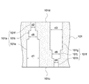
図2に示すように、第1貫通孔101a内には第1内部電極104が、第2貫通孔101b内には第2内部電極105がそれぞれ形成される。したがって、第1貫通孔101aと第2貫通孔101bの配列は第1内部電極104と第2内部電極105の配列に等しい。図4には、第1貫通孔101aと第2貫通孔101bは交互に配列されているように示されているが、ランダムに配列されていてもよい。第1貫通孔101aと第2貫通孔101bの数的割合は同数でなくてもよいが、同数に近い方が、第1内部電極104と第2内部電極105の数が同数に近くなり、コンデンサ100の容量が大きくなるため、好適である。
As shown in FIG. 2, a first
第1外部電極層102は図2に示すように、誘電体層101の第1の面101c上に配設されている。第1外部電極層102は導電性材料、例えば、Cu、Ni、Cr、Ag、Pd、Fe、Sn、Pb、Pt、Ir、Rh、Ru、Al、Ti等の純金属やこれらの合金であるものとすることができる。第1外部電極層102の厚さは例えば数十nm〜数μmであるものとすることができる。また、第1外部電極層102は、複数層の導電性材料が積層されるように配設されたものとすることも可能である。
As shown in FIG. 2, the first
第2外部電極層103は図2に示すように、誘電体層101の第2の面101d上に配設されている。第2外部電極層102は、第1外部電極層102と同様の導電性材料からなるものとすることができ、その厚さは例えば数nm〜数μmであるものとすることができる。第2外部電極層103の構成材料は第1外部電極層102の構成材料と同一でもよく異なっていてもよい。また、第2外部電極層102も、複数層の導電性材料が積層されるように配設されたものとすることが可能である。
As shown in FIG. 2, the second
第1内部電極104は、コンデンサ100の一方の対向電極として機能する。図2に示すように第1内部電極104は、第1貫通孔101aに形成され、第1外部電極層102に接続されている。図6は、第1内部電極104及び第2内部電極105の形状を示す拡大図である。同図に示すように第1内部電極104は、第1貫通孔101aの形状(2段階の孔径)にしたがって、2段階の径(電極径)を有し、第1外部電極層102から、第1貫通孔101aの第1孔径部101eを介して第2孔径部101fの途中まで形成されている。即ち、第1内部電極104は、一端が第1外部電極層102に接続され、他端すなわちその先端は第2孔径部101f内に位置して第2外部電極層103と離間している。第1内部電極104と第2外部電極層103の間は空間とすることができ、またこの間に絶縁体を配置することも可能である。
The first
第1内部電極104は、導電性材料、例えばCu、Ni、Co、Cr、Ag、Au、Pd、Fe、Sn、Pb、Pt等の純金属やこれらの合金からなるものとすることが可能である。
The first
第2内部電極105は、コンデンサ100の他方の対向電極として機能する。図2に示すように第2内部電極105は、第2貫通孔101bに形成され、第2外部電極層103に接続されている。図6に示すように第2内部電極105は、第2貫通孔101bの形状(2段階の孔径)にしたがって、2段階の径(電極径)を有し、第2外部電極層103から、第2貫通孔101bの第3孔径部101gを介して第4孔径部101hの途中まで形成されている。即ち、第2内部電極105は、一端が第2外部電極層103に接続され、他端すなわちその先端は第4孔径部101h内に位置して第1外部電極層102と離間している。第2内部電極105と第1外部電極層102の間は空間とすることができ、またこの間に絶縁体を配置することも可能である。
The second
第2内部電極105は、第1内部電極104と同様に導電性材料、例えばCu、Ni、Co、Cr、Ag、Au、Pd、Fe、Sn、Pb、Pt等の純金属やこれらの合金からなるものとすることが可能である。なお、第2内部電極105の材料は、第1内部電極104の材料と同一でもよく、異なってもよい。
Similar to the first
(コンデンサの効果)
コンデンサ100は以上のような構成を有する。図2に示すように、第1内部電極104と第2内部電極105が誘電体層101を介して互いに対向しており、これによりコンデンサが構成されている。第1内部電極104は第1外部電極層102に導通しており、第1外部電極層102を介して外部と接続される。第2内部電極105は第2外部電極層103に導通しており、第2外部電極層103を介して外部と接続される。
(Capacitor effect)
The
上述のように第1内部電極104と第2外部電極層103の間は絶縁されているが、第1内部電極104の先端に電界が集中する。このため、第1内部電極104と第2内部電極105の間の絶縁性は、第1内部電極104の先端を囲む誘電体層101の厚さ(壁厚)によって左右される。なお第1内部電極104と第2外部電極層103との間には空間(または絶縁体)が存在するため、容易に十分な絶縁性を確保することができる。ここで、本実施形態においては、第1内部電極104の先端近傍は第2孔径部101f内に形成され(図6参照)、厚い誘電体層101の壁に囲まれているため、第1内部電極104と第2内部電極105の間の絶縁性が向上している。
As described above, the first
一方、第1内部電極104の大部分は、第1孔径部101e内に形成されている。一般的に、コンデンサは、誘電体によって隔てられる対向電極間の距離が小さい方が容量が大きくなる。ここで、第1内部電極104の大部分と対向する第2内部電極105の間は、薄い誘電体層101の壁によって隔てられているため、コンデンサ100の容量は維持される。
On the other hand, most of the first
仮に、第1孔径部101eの孔径d1が第2孔径部101fの孔径d2と同一であり、即ち第1貫通孔101aが単一の孔径を有する場合には、対向電極間の距離が大きくなり、絶縁性が向上する替わりにコンデンサ容量が低下することになる。これに対し、本実施形態に係る誘電体層101では、電極先端部近傍だけに限定して対向電極間の距離が大きくなっているので、コンデンサ容量の低下がほとんど生じない。
If the hole diameter d1 of the first
このように、本実施形態に係る第1貫通孔101aにおいては、第2孔径部101fと第1孔径部101eが形成されていることにより、第1内部電極104と第2内部電極105の間の絶縁性の向上と、コンデンサ100の容量の維持を共に実現することが可能である。
As described above, in the first through
第2内部電極105の場合も同様である。即ち、第2内部電極105と第1内部電極104の間は絶縁されているが、第2内部電極105の先端に電界が集中する。このため、第2内部電極105と第1内部電極104の間の絶縁性は、第2内部電極105の先端を囲む誘電体層101の厚さ(壁厚)によって左右される。ここで、本実施形態においては、第2内部電極105の先端は第4孔径部101h内に形成され(図6参照)、厚い誘電体層101の壁に囲まれているため、第2内部電極105と第1内部電極104の間の絶縁性が向上している。
The same applies to the second
一方、第2内部電極105の大部分は、第3孔径部101g内に形成されている。これにより、第2内部電極105の大部分と対向する第1内部電極104の間は、薄い誘電体層101の壁によって隔てられているため、コンデンサ100の容量は維持される。このように、本実施形態に係る第2貫通孔101bにおいても、第4孔径部101hと第3孔径部101gが形成されていることにより、第2内部電極105と第1内部電極105の間の絶縁性の向上と、コンデンサ100の容量の維持を共に実現することが可能である。
On the other hand, most of the second
以上のように、本実施形態に係るコンデンサ100においては、誘電体層101にそれぞれ2段階の孔径を有する第1貫通孔101aと第2貫通孔101bが形成されていることにより、コンデンサ容量の維持と絶縁破壊耐圧の向上を同時に実現することが可能である。具体的には、本実施形態の構成を採用しないコンデンサ(貫通孔の孔径が均一)の絶縁破壊耐圧は10〜15Vであったが、本実施形態に係る構成を有するコンデンサ(大孔径の孔径部で前記孔径が同一となるコンデンサ)では絶縁破壊耐圧が20〜25Vに改善した実験結果が得られている。一方、本実施形態のコンデンサ容量値は2.3%の低下しかみられなかった。なお結果データはN=50の平均値を採用した。
As described above, in the
(コンデンサの製造方法)
上述したコンデンサ100の製造方法について説明する。なお、以下に示す製造方法は一例であり、コンデンサ100は、以下に示す製造方法とは異なる製造方法によって製造することも可能である。図7乃至12は、コンデンサ100の製造プロセスを示す模式図である。
(Capacitor manufacturing method)
A method for manufacturing the
図7(a)は、誘電体層101の元となる基材301を示す。誘電体層101を金属酸化物(例えば酸化アルミニウム)からなるものとする場合、基材301はその酸化前の金属(例えばアルミニウム)である。
FIG. 7A shows a
図7(b)に示すように、例えば15℃〜20℃に調整されたシュウ酸(0.1mol/l)溶液中で基材301を陽極として電圧を印加すると、基材301が酸化(陽極酸化)され、基材酸化物302が形成される。この際、基材酸化物302の自己組織化作用によって、基材酸化物302に孔Hが形成される。孔Hは酸化の進行方向、即ち基材301の厚み方向に向かって成長する。なお、孔Hの孔径が上述した孔径d1及び孔径d3(図5参照)に相当する。
As shown in FIG. 7B, for example, when a voltage is applied with the
なお、陽極酸化の前に基材301に規則的なピット(凹部)を形成しておき、このピットを基点として孔Hを成長させてもよい。ピットの配置により貫通孔(第1貫通孔101a及び第2貫通孔101b)の配列を制御することが可能となるからである。ピットは、例えば基材301にモールド(型)を押圧することによって形成することが可能である。
Note that regular pits (concave portions) may be formed in the
所定時間経過後、基材301に印加されている電圧を増加させる。自己組織化によって形成される孔Hのピッチは、印加電圧の大きさによって決定されるため、孔Hのピッチが拡大するように自己組織化が進行する。これにより、図7(c)に示すように一部の孔Hについて孔の形成が継続すると共に、孔径が拡大する。一方で、孔Hのピッチが拡大したことによって、他の孔Hについては孔の形成が停止する。以下、孔の形成が停止した孔Hを孔H1とし、孔の形成が継続した(拡大した)孔Hを孔H2とする。
After a predetermined time has elapsed, the voltage applied to the
陽極酸化の条件は適宜設定可能であり、例えば、図7(b)に示す1段階目の陽極酸化の印加電圧は数V〜数100V、処理時間は数分〜数日に設定することができる。図7(c)に示す2段階目の陽極酸化の印加電圧では、電圧値を1段階目の数倍とし、処理時間は数分〜数十分に設定することができる。 The anodizing conditions can be set as appropriate. For example, the applied voltage of the first stage anodizing shown in FIG. 7B can be set to several volts to several hundred volts, and the processing time can be set to several minutes to several days. . With the applied voltage of the second stage of anodic oxidation shown in FIG. 7C, the voltage value can be several times that of the first stage, and the processing time can be set to several minutes to several tens of minutes.
例えば、1段階目の印加電圧を40Vとすることにより孔径が100nmの孔Hが形成され、2段階目の印加電圧を80Vとすることにより孔H2の孔径が200nmに拡大される。2段階目の電圧値を上述した範囲内とすることにより、孔H1と孔H2の数を概ね同等とすることが可能である。また、2段階目の電圧印加の処理時間を上述の範囲内とすることにより、孔H2のピッチ変換が十分に完了しつつ、2段階目の電圧印加によって底部に形成される基材酸化物302の厚さを小さくすることができる。2段階目の電圧印加で形成される基材酸化物302は、後の工程で除去されるため、できるだけ薄いことが好ましい。
For example, a hole H having a hole diameter of 100 nm is formed by setting the applied voltage at the first stage to 40V, and a hole diameter of the hole H2 is expanded to 200 nm by setting the applied voltage at the second stage to 80V. By setting the voltage value of the second stage within the above-described range, the number of holes H1 and holes H2 can be made substantially equal. Further, by setting the processing time of the second stage voltage application within the above-mentioned range, the
続いて、図8(a)に示すように、酸化されていない基材301を除去する。基材301の除去は、例えばウェットエッチングによってすることができる。以降、基材酸化物302の孔H1及び孔H2が形成された側の面を表面302aとし、その反対側の面を裏面302bとする。
Subsequently, as shown in FIG. 8A, the
続いて、図8(b)に示すように基材酸化物302を裏面302b側から所定の厚さで除去する。これは反応性イオンエッチング(RIE:Reactive Ion Etching)によってすることができる。この際、孔H2が裏面302bに連通し、孔H1は裏面302bに連通しない程度の厚さで、基材酸化物302を除去する。
Subsequently, as shown in FIG. 8B, the
続いて、図8(c)に示すように、表面302aに導電性材料からなる第1導体層303を成膜する。第1導体層303は、スパッタ法、真空蒸着法等、任意の方法によって成膜することが可能である。
Subsequently, as shown in FIG. 8C, a
続いて、図9(a)に示すように、孔H2内に導電性材料からなる第1内部導体部分304を埋め込むする。第1内部導体部分304は、第1導体層303をシード層として基材酸化物302に電解めっきを施すことによって埋め込むことが可能である。孔H1にはめっき液が侵入しないため、孔H1内には第1内部導体部分304は形成されない。
Subsequently, as shown in FIG. 9A, a first
続いて、図9(b)に示すように、基材酸化物302を膨張させる。基材酸化物302を、沸騰水蒸気中に数秒から数分程度曝すことによって膨張させることが可能である。これにより、孔H2の孔径が、孔径d3から孔径d4に減少する(図5参照)。なお、孔H2において、既に第1内部導体部分304が埋め込まれる部分は、第1内部導体部分304が存在することによって孔径が減少せず、孔径d3のままとなる。
Subsequently, as shown in FIG. 9B, the
続いて、図9(c)に示すように孔H2内に導電性材料からなる第2内部導体部分305を埋め込む。第2内部導体部分305は、第1導体層303をシード層として基材酸化物302に電解めっきを施すことによって埋め込むことが可能である。上述のように孔H2は孔径が減少しているため、第2内部導体部分305の径は第1内部導体部分304の径より小さくなる。第2内部導体部分305は、孔H2において孔径d4の部分の途中まで形成する。以下、第1内部導体部分304と第2内部導体部分305を合わせて第1内部導体306とする。
Subsequently, as shown in FIG. 9C, a second
続いて、図10(a)に示すように、第1導体層303を除去する。第1導体層303の除去は、ウェットエッチング法、ドライエッチング法、イオンミリング法、CMP(Chemical Mechanical Polishing)法等によってすることができる。
Subsequently, as shown in FIG. 10A, the
続いて、図10(b)に示すように基材酸化物302を裏面302bから所定の厚さで、再度除去する。これは、反応性イオンエッチングによってすることができる。この際、孔H1が裏面302bに連通し、第1内部導体306が裏面302bに露出しない程度の厚さで、基材酸化物302を除去する。
Subsequently, as shown in FIG. 10B, the
ここで、孔H2において第1内部導体306が形成されていない空隙はそのままでもよく、絶縁体を封入してもよい。絶縁体は基材酸化物302と同様の金属酸化物、電着可能な樹脂材料(例えばポリイミド、エポキシ、アクリル等)、SiO等とすることができる。空隙の厚さは、コンデンサ100の素子容量、絶縁破壊耐圧等に応じて設定することができ、例えば数十nmから数十μmとすることができる。
Here, the gap in which the first
続いて、図10(c)に示すように、裏面302bに導電性材料からなる第2導体層307を成膜する。第2導体層307は、スパッタ法、真空蒸着法等、任意の方法によって成膜することが可能である。
Subsequently, as shown in FIG. 10C, a
続いて、図11(a)に示すように、孔H1内に導電性材料からなる第3内部導体部分308を埋め込む。第3内部導体部分308は、第2導体層307をシード層として基材酸化物302に電解めっきを施すことによって埋め込むことが可能である。なお、第1内部導体306は第2導体層307と離間し、絶縁されているため、電解めっきを受けない。
Subsequently, as shown in FIG. 11A, a third
続いて、図11(b)に示すように、再度基材酸化物302を膨張させる。基材酸化物302を、沸騰水蒸気中に数秒から数分程度曝すことによって膨張させることが可能である。これにより、孔H1の孔径が、孔径d1から孔径d2に減少する(図5参照)。なお、孔H1において、既に第3内部導体部分308が埋め込まれる領域は、第3内部導体部分308が存在することによって孔径が減少せず、孔径d1のままとなる。
Subsequently, as shown in FIG. 11B, the
続いて、図11(c)に示すように孔H1内に導電性材料からなる第4内部導体部分309を埋め込む。第4内部導体部分309は、第2導体層307をシード層として基材酸化物302に電解めっきを施すことによって埋め込むことが可能である。上述のように孔H1は孔径が減少しているため、第4内部導体部分309の径は第3内部導体部分308の径より小さくなる。第4内部導体部分309は、孔H1において孔径d2の部分の途中まで形成する。以下、第3内部導体部分308と第4内部導体部分309を合わせて第2内部導体310とする。
Subsequently, as shown in FIG. 11C, a fourth
ここで、孔H1において第2内部導体310が形成されていない空隙はそのままでもよく、絶縁体を封入してもよい。絶縁体は基材酸化物302と同様の金属酸化物、電着可能な樹脂材料(例えばポリイミド、エポキシ、アクリル等)、SiO等とすることができる。空隙の厚さは、コンデンサ100の素子容量、絶縁破壊耐圧等に応じて設定することができ、例えば数十nmから数十μmとすることができる。
Here, the gap in which the second
続いて、図12に示すように、表面302aに導電性材料からなる第3導体層311を成膜する。第3導体層311は、スパッタ法、真空蒸着法等、任意の方法によって第1内部導体306と導通するように成膜することが可能である。
Subsequently, as shown in FIG. 12, a
以上のようにして、図2に示すコンデンサ100を製造することが可能である。なお、基材酸化物302は誘電体層101に、第2導体層307は第1外部電極層102に、第3導体層311は第2外部電極層103にそれぞれ対応する。同様に第1内部導体306は第2内部電極105に、第2内部導体310は第1内部電極104にそれぞれ対応する。
As described above, the
(コンデンサの変形例)
図13は、本実施形態の変形例に係るコンデンサ100を示す模式図である。同図に示すように、変形例に係るコンデンサ100の誘電体層101において、第1貫通孔101aは、上記実施形態と同様に、大孔径の孔径部と小孔径の孔径部を有するものとすることができる。一方で、第2貫通孔101bは、上記実施形態と異なり、ほぼ均一な孔径を有するように形成されている。
(Capacitor variants)
FIG. 13 is a schematic diagram showing a
このような構成によっても、コンデンサ100の容量を維持しつつ、少なくとも第1内部電極104と第2内部電極104の絶縁性を向上させることが可能である。
Even with such a configuration, it is possible to improve the insulation of at least the first
このようなコンデンサ100は、上述した製造方法と類似の製造方法によって製造することが可能である。具体的には図11(b)(c)のプロセスをおこなわずに、上述した製造方法において2回ずつ実施した、基材酸化物302を膨張させる工程と内部導体を埋め込む工程を1回ずつとすればよい。
Such a
図14は、本実施形態の別の変形例に係るコンデンサ100を示す模式図である。図15は、同コンデンサ100の誘電体層101の拡大図である。これらの図に示すように、
第1貫通孔101aは、第1孔径部101e及び第2孔径部101fに加え、第5孔径部101iを有する。第5孔径部101iは、第1孔径部101eと第2孔径部101fの間に形成され、第5孔径部101iの孔径d5は、第1孔径部101eの孔径d1より小さく、第2孔径部101fの孔径d2より大きい。
FIG. 14 is a schematic diagram showing a
The first through
第2貫通孔101bも同様に、第3孔径部101g及び第4孔径部101hに加え、第6孔径部101jを有する。第6孔径部101jは、第3孔径部101gと第4孔径部101hの間に形成され、第6孔径部101jの孔径d6は、第3孔径部101gの孔径d3より小さく、第4孔径部101hの孔径d4より大きい。
Similarly, the second through
第1内部電極104は図14に示すように、第1貫通孔101aの形状に応じて形成され、第1外部電極層102から、第1孔径部101e及び第5孔径部101iを介して第2孔径部101fの途中まで形成されている(図15参照)。第2内部電極105も図14に示すように、第2貫通孔101bの形状に応じて形成され、第2外部電極層103から、第3孔径部101g及び第6孔径部101jを介して第4孔径部101hの途中まで形成されている(図15参照)。
As shown in FIG. 14, the first
上記実施形態のように、第1貫通孔101aに第2孔径部101fと第5孔径部101iを設けたことにより、段差コーナー部(孔径の段差)が2カ所となって該部への電界集中は分散される。したがって第1内部電極104の段差コーナー部を起点とした絶縁破壊を防止することができる。こうして第1内部電極104と第2内部電極105の間の絶縁性がさらに向上する。
As in the above embodiment, by providing the first through
第2貫通孔101bについても同様に、第2貫通孔101bに第4孔径部101hおよび第6孔径部101jを設けたことにより、段差コーナー部への電界集中をさらに分散させることができるので、第2内部電極105と第1内部電極104の絶縁性がさらに向上する。
Similarly, the second through
即ち、この変形例に係るコンデンサ100においては、コンデンサ容量を維持しつつ、絶縁破壊耐圧をさらに向上させることが可能である。また、第1貫通孔101a及び第2貫通孔101bの孔径はそれぞれ3段階としたがこれに限られず、さらに多段階の孔径部を有するものとすることが可能であり、要求されるコンデンサ容量と絶縁破壊耐圧のバランスによって決定することが可能である。
That is, in the
このような構成を有するコンデンサ100は、上述した製造方法と類似の製造方法によって製造することが可能である。即ち基材酸化物302を膨張させる工程と内部導体を埋め込む工程を、目的の孔径の段数に合わせて複数回実施すればよい。
以上、本発明の実施形態について説明したが、本発明は上述の実施形態にのみ限定されるものではなく、本発明の要旨を逸脱しない範囲内において種々変更を加え得ることは勿論である。 The embodiment of the present invention has been described above, but the present invention is not limited to the above-described embodiment, and it is needless to say that various modifications can be made without departing from the gist of the present invention.
100…コンデンサ
101…誘電体層
101a…第1貫通孔
101b…第2貫通孔
101c…第1の面
101d…第2の面
102…第1外部電極層
103…第2外部電極層
104…第1内部電極
105…第2内部電極
DESCRIPTION OF
Claims (5)
前記第1の面に配設された第1の外部電極層と、
前記第2の面に配設された第2の外部電極層と、
前記第1の貫通孔内に形成され、前記第1の外部電極層に接続し、先端が前記第2の孔径部に位置して前記第2の外部電極層と離間する第1の内部電極と、
前記第2の貫通孔内に形成され、前記第2の外部電極層に接続し、前記第1の外部電極層と離間する第2の内部電極と
を具備するコンデンサ。 A dielectric layer comprising a first surface, a second surface opposite to the first surface, and a plurality of through holes communicating with the first surface and the second surface, The through hole includes a first through hole and a second through hole, and the first through hole has a first hole diameter portion having a first hole diameter and the first hole diameter on the second surface side. A dielectric layer having a second hole diameter portion having a smaller second hole diameter;
A first external electrode layer disposed on the first surface;
A second external electrode layer disposed on the second surface;
A first internal electrode formed in the first through-hole, connected to the first external electrode layer and having a tip located at the second hole diameter portion and spaced apart from the second external electrode layer; ,
Wherein formed in the second through hole, the capacitor second connected to an external electrode layer, and second inner electrodes apart from the first external electrode layer.
前記第2の貫通孔は、第3の孔径を有する第3の孔径部と、前記第1の面側において前記第3の孔径より小さい第4の孔径を有する第4の孔径部とを有し、
前記第2の内部電極は、先端が前記第4の孔径部に位置する
コンデンサ。 The capacitor according to claim 1,
The second through hole has a third hole diameter portion having a third hole diameter, and a fourth hole diameter portion having a fourth hole diameter smaller than the third hole diameter on the first surface side. ,
The second internal electrode is a capacitor whose tip is located in the fourth hole diameter portion .
前記第1の貫通孔は、前記第1の孔径部と前記第2の孔径部の間において、前記第1の孔径より小さく前記第2の孔径より大きい第5の孔径を有する第5の孔径部をさらに有し、
前記第2の貫通孔は、前記第3の孔径部と前記第4の孔径部の間において、前記第3の孔径より小さく前記第4の孔径より大きい第6の孔径を有する第6の孔径部をさらに有する
コンデンサ。 The capacitor according to claim 2,
The first through-hole has a fifth hole diameter portion having a fifth hole diameter smaller than the first hole diameter and larger than the second hole diameter between the first hole diameter portion and the second hole diameter portion. Further comprising
The second through hole has a sixth hole diameter that is smaller than the third hole diameter and larger than the fourth hole diameter between the third hole diameter part and the fourth hole diameter part. Further having a capacitor.
前記誘電体層は、陽極酸化作用によって貫通孔を生じる材料からなる
コンデンサ。 The capacitor according to claim 1,
The dielectric layer is a capacitor made of a material that generates a through hole by an anodizing action.
前記誘電体層は、酸化アルミニウムからなる
コンデンサ。 The capacitor according to claim 4,
The dielectric layer is a capacitor made of aluminum oxide.
Priority Applications (4)
| Application Number | Priority Date | Filing Date | Title |
|---|---|---|---|
| JP2012191162A JP6043548B2 (en) | 2012-08-31 | 2012-08-31 | Capacitor |
| KR20130091889A KR20140029176A (en) | 2012-08-31 | 2013-08-02 | Capacitor |
| US14/013,341 US9076595B2 (en) | 2012-08-31 | 2013-08-29 | Capacitor |
| US14/742,241 US9230742B2 (en) | 2012-08-31 | 2015-06-17 | Capacitor |
Applications Claiming Priority (1)
| Application Number | Priority Date | Filing Date | Title |
|---|---|---|---|
| JP2012191162A JP6043548B2 (en) | 2012-08-31 | 2012-08-31 | Capacitor |
Publications (3)
| Publication Number | Publication Date |
|---|---|
| JP2014049600A JP2014049600A (en) | 2014-03-17 |
| JP2014049600A5 JP2014049600A5 (en) | 2015-07-23 |
| JP6043548B2 true JP6043548B2 (en) | 2016-12-14 |
Family
ID=50187280
Family Applications (1)
| Application Number | Title | Priority Date | Filing Date |
|---|---|---|---|
| JP2012191162A Active JP6043548B2 (en) | 2012-08-31 | 2012-08-31 | Capacitor |
Country Status (3)
| Country | Link |
|---|---|
| US (2) | US9076595B2 (en) |
| JP (1) | JP6043548B2 (en) |
| KR (1) | KR20140029176A (en) |
Families Citing this family (7)
| Publication number | Priority date | Publication date | Assignee | Title |
|---|---|---|---|---|
| JP6218558B2 (en) * | 2013-10-30 | 2017-10-25 | 太陽誘電株式会社 | Capacitor |
| JP2015179753A (en) * | 2014-03-19 | 2015-10-08 | 太陽誘電株式会社 | capacitor |
| CN106328376A (en) * | 2015-07-03 | 2017-01-11 | 华硕电脑股份有限公司 | Manufacturing method of capacitor |
| KR101811851B1 (en) * | 2016-06-09 | 2017-12-22 | (주)포인트엔지니어링 | Three-dimensional capacitor |
| JP7195866B2 (en) * | 2018-10-17 | 2022-12-26 | キヤノン株式会社 | LIQUID EJECTION HEAD AND MANUFACTURING METHOD THEREOF |
| DE112020006876T5 (en) * | 2020-03-12 | 2022-12-29 | Rohm Co., Ltd. | CAPACITOR AND METHOD OF MAKING A CAPACITOR |
| US11715594B2 (en) * | 2021-05-27 | 2023-08-01 | International Business Machines Corporation | Vertically-stacked interdigitated metal-insulator-metal capacitor for sub-20 nm pitch |
Family Cites Families (20)
| Publication number | Priority date | Publication date | Assignee | Title |
|---|---|---|---|---|
| JP2711618B2 (en) * | 1992-06-30 | 1998-02-10 | ティーディーケイ株式会社 | Dielectric composition, multilayer wiring board and multilayer ceramic capacitor |
| US6034864A (en) * | 1997-11-14 | 2000-03-07 | Murata Manufacturing Co., Ltd. | Multilayer capacitor |
| US6072690A (en) * | 1998-01-15 | 2000-06-06 | International Business Machines Corporation | High k dielectric capacitor with low k sheathed signal vias |
| JP2001189234A (en) * | 1999-12-28 | 2001-07-10 | Tdk Corp | Layered capacitor |
| JP3878439B2 (en) | 2001-06-27 | 2007-02-07 | シャープ株式会社 | Porous layer and device, and manufacturing method thereof |
| US6757152B2 (en) * | 2001-09-05 | 2004-06-29 | Avx Corporation | Cascade capacitor |
| US20040108134A1 (en) * | 2002-10-11 | 2004-06-10 | Borland William J. | Printed wiring boards having low inductance embedded capacitors and methods of making same |
| US7230316B2 (en) * | 2002-12-27 | 2007-06-12 | Semiconductor Energy Laboratory Co., Ltd. | Semiconductor device having transferred integrated circuit |
| JP4213978B2 (en) * | 2003-03-26 | 2009-01-28 | 京セラ株式会社 | Multilayer electronic component and manufacturing method thereof |
| JP3901697B2 (en) * | 2004-03-19 | 2007-04-04 | Tdk株式会社 | Multilayer capacitor |
| KR100674842B1 (en) * | 2005-03-07 | 2007-01-26 | 삼성전기주식회사 | Print Circuit Board Having the Embedded Multilayer Chip Capacitor |
| JP4907594B2 (en) | 2007-06-14 | 2012-03-28 | 太陽誘電株式会社 | Capacitor and manufacturing method thereof |
| JP4956405B2 (en) * | 2007-07-30 | 2012-06-20 | 太陽誘電株式会社 | Capacitor element and method of manufacturing capacitor element |
| US8027145B2 (en) * | 2007-07-30 | 2011-09-27 | Taiyo Yuden Co., Ltd | Capacitor element and method of manufacturing capacitor element |
| JP4382841B2 (en) * | 2007-08-20 | 2009-12-16 | 太陽誘電株式会社 | Capacitor and manufacturing method thereof |
| JP4493686B2 (en) * | 2007-09-27 | 2010-06-30 | 太陽誘電株式会社 | Capacitor and manufacturing method thereof |
| US7965492B2 (en) * | 2007-10-19 | 2011-06-21 | Oh Young Joo | Metal capacitor and manufacturing method thereof |
| JP2012114121A (en) * | 2010-11-19 | 2012-06-14 | Taiyo Yuden Co Ltd | Capacitor and method for manufacturing the same |
| JP5665617B2 (en) * | 2011-03-17 | 2015-02-04 | 太陽誘電株式会社 | Capacitor configuration unit and capacitor |
| JP5904765B2 (en) * | 2011-11-10 | 2016-04-20 | 太陽誘電株式会社 | Capacitor and manufacturing method thereof |
-
2012
- 2012-08-31 JP JP2012191162A patent/JP6043548B2/en active Active
-
2013
- 2013-08-02 KR KR20130091889A patent/KR20140029176A/en not_active Application Discontinuation
- 2013-08-29 US US14/013,341 patent/US9076595B2/en active Active
-
2015
- 2015-06-17 US US14/742,241 patent/US9230742B2/en active Active
Also Published As
| Publication number | Publication date |
|---|---|
| US20150287534A1 (en) | 2015-10-08 |
| US9076595B2 (en) | 2015-07-07 |
| KR20140029176A (en) | 2014-03-10 |
| JP2014049600A (en) | 2014-03-17 |
| US20140063690A1 (en) | 2014-03-06 |
| US9230742B2 (en) | 2016-01-05 |
Similar Documents
| Publication | Publication Date | Title |
|---|---|---|
| JP6043548B2 (en) | Capacitor | |
| JP6543622B2 (en) | Structure with improved capacitor | |
| JP5416840B2 (en) | Capacitor and manufacturing method thereof | |
| US8134826B2 (en) | Capacitor and method of manufacturing the same | |
| JP5432002B2 (en) | Capacitor and manufacturing method thereof | |
| KR100834833B1 (en) | Capacitor, circuit board with built-in capacitor and method for producting the same | |
| US8023249B2 (en) | Capacitor and method of manufacturing the same | |
| JP6840502B2 (en) | Manufacturing methods for microstructures, electronic components, circuit modules and electronic devices | |
| JP5931594B2 (en) | Capacitor | |
| JP5750092B2 (en) | Capacitor | |
| JP6343529B2 (en) | Electronic components, circuit modules and electronic equipment | |
| US20140009866A1 (en) | Capacitor, structure and method of forming capacitor | |
| KR101538538B1 (en) | Capacitor, structure and method of forming capacitor | |
| JP6218558B2 (en) | Capacitor | |
| JP6218660B2 (en) | Capacitor | |
| JP2013201318A (en) | Porous capacitor | |
| US20140226257A1 (en) | Capacitor and method of manufacturing capacitor | |
| JP2005093597A (en) | Thin film capacitor and its manufacturing method | |
| WO2015076079A1 (en) | Capacitor | |
| JP2016004827A (en) | Capacitor, circuit module, and mobile communication equipment | |
| JP2015122467A (en) | Capacitor | |
| WO2015141617A1 (en) | Capacitor | |
| JP2017188563A (en) | Capacitor and method of manufacturing capacitor | |
| US20160189874A1 (en) | Electrode structure for capacitor, electrolytic capacitor, and method of manufacturing the same |
Legal Events
| Date | Code | Title | Description |
|---|---|---|---|
| A521 | Request for written amendment filed |
Free format text: JAPANESE INTERMEDIATE CODE: A523 Effective date: 20150604 |
|
| A621 | Written request for application examination |
Free format text: JAPANESE INTERMEDIATE CODE: A621 Effective date: 20150622 |
|
| A977 | Report on retrieval |
Free format text: JAPANESE INTERMEDIATE CODE: A971007 Effective date: 20160316 |
|
| A131 | Notification of reasons for refusal |
Free format text: JAPANESE INTERMEDIATE CODE: A131 Effective date: 20160322 |
|
| A521 | Request for written amendment filed |
Free format text: JAPANESE INTERMEDIATE CODE: A523 Effective date: 20160520 |
|
| TRDD | Decision of grant or rejection written | ||
| A01 | Written decision to grant a patent or to grant a registration (utility model) |
Free format text: JAPANESE INTERMEDIATE CODE: A01 Effective date: 20161101 |
|
| A61 | First payment of annual fees (during grant procedure) |
Free format text: JAPANESE INTERMEDIATE CODE: A61 Effective date: 20161114 |
|
| R150 | Certificate of patent or registration of utility model |
Ref document number: 6043548 Country of ref document: JP Free format text: JAPANESE INTERMEDIATE CODE: R150 |
|
| R250 | Receipt of annual fees |
Free format text: JAPANESE INTERMEDIATE CODE: R250 |
|
| R250 | Receipt of annual fees |
Free format text: JAPANESE INTERMEDIATE CODE: R250 |
|
| R250 | Receipt of annual fees |
Free format text: JAPANESE INTERMEDIATE CODE: R250 |
|
| R250 | Receipt of annual fees |
Free format text: JAPANESE INTERMEDIATE CODE: R250 |
|
| R250 | Receipt of annual fees |
Free format text: JAPANESE INTERMEDIATE CODE: R250 |