JP5432002B2 - Capacitor and manufacturing method thereof - Google Patents
Capacitor and manufacturing method thereof Download PDFInfo
- Publication number
- JP5432002B2 JP5432002B2 JP2010041129A JP2010041129A JP5432002B2 JP 5432002 B2 JP5432002 B2 JP 5432002B2 JP 2010041129 A JP2010041129 A JP 2010041129A JP 2010041129 A JP2010041129 A JP 2010041129A JP 5432002 B2 JP5432002 B2 JP 5432002B2
- Authority
- JP
- Japan
- Prior art keywords
- hole
- electrode
- oxide
- capacitor
- internal electrode
- Prior art date
- Legal status (The legal status is an assumption and is not a legal conclusion. Google has not performed a legal analysis and makes no representation as to the accuracy of the status listed.)
- Active
Links
Images

Classifications
-
- H—ELECTRICITY
- H01—ELECTRIC ELEMENTS
- H01G—CAPACITORS; CAPACITORS, RECTIFIERS, DETECTORS, SWITCHING DEVICES, LIGHT-SENSITIVE OR TEMPERATURE-SENSITIVE DEVICES OF THE ELECTROLYTIC TYPE
- H01G9/00—Electrolytic capacitors, rectifiers, detectors, switching devices, light-sensitive or temperature-sensitive devices; Processes of their manufacture
- H01G9/145—Liquid electrolytic capacitors
-
- H—ELECTRICITY
- H01—ELECTRIC ELEMENTS
- H01G—CAPACITORS; CAPACITORS, RECTIFIERS, DETECTORS, SWITCHING DEVICES, LIGHT-SENSITIVE OR TEMPERATURE-SENSITIVE DEVICES OF THE ELECTROLYTIC TYPE
- H01G4/00—Fixed capacitors; Processes of their manufacture
- H01G4/002—Details
- H01G4/018—Dielectrics
- H01G4/06—Solid dielectrics
-
- H—ELECTRICITY
- H01—ELECTRIC ELEMENTS
- H01G—CAPACITORS; CAPACITORS, RECTIFIERS, DETECTORS, SWITCHING DEVICES, LIGHT-SENSITIVE OR TEMPERATURE-SENSITIVE DEVICES OF THE ELECTROLYTIC TYPE
- H01G13/00—Apparatus specially adapted for manufacturing capacitors; Processes specially adapted for manufacturing capacitors not provided for in groups H01G4/00 - H01G11/00
- H01G13/006—Apparatus or processes for applying terminals
Landscapes
- Engineering & Computer Science (AREA)
- Power Engineering (AREA)
- Microelectronics & Electronic Packaging (AREA)
- Manufacturing & Machinery (AREA)
- Fixed Capacitors And Capacitor Manufacturing Machines (AREA)
Description
本発明は、コンデンサ及びその製造方法に関し、更に具体的には、容量密度の向上,製造プロセスの簡略化,高周波特性の向上,誘電体材料の汎用性の向上に関するものである。 The present invention relates to a capacitor and a method for manufacturing the same, and more specifically to an improvement in capacitance density, simplification of a manufacturing process, improvement in high-frequency characteristics, and improvement in versatility of dielectric materials.
現在広く用いられているコンデンサとして、Al電解コンデンサや積層セラミックコンデンサが知られている。Al電解コンデンサでは、電解液を使うために、液漏れなどの問題がある。また、積層セラミックコンデンサでは焼成が必要であり、電極と誘電体間における熱収縮などの問題がある。これらを改善する技術として、例えば、下記特許文献1〜3には、ポーラスAl2O3を応用したコンデンサが提案されている。
Al capacitors and multilayer ceramic capacitors are known as capacitors that are currently widely used. Since an Al electrolytic capacitor uses an electrolytic solution, there are problems such as liquid leakage. In addition, the multilayer ceramic capacitor needs to be fired, and there is a problem such as heat shrinkage between the electrode and the dielectric. As a technique for improving these, for example,
特許文献1には、上述したポーラスAl2O3を利用し、正負電極がランダムに振り分けられたコンデンサ及びその製造方法が開示されている。当該技術によれば、弁金属の1段目の陽極酸化において所望の深さのホールを形成し(同公報の第2図(C))、引き続き、1段目よりも大きい電圧で陽極酸化を行う(第2図(D))。陽極酸化で発生するホールのピッチは電圧に比例するため、大きい電圧で処理されたホールはピッチが大きくなり、1段目で形成されたホールの一部と接続される。引き続き、2段目のホールの底を開口(第2図(E)及び(F))してメッキを埋め込むと、2段目に接続された1段目のホールのみに導体が埋め込まれ、2段目に接続されない1段目のホールには導体が埋め込まれない(第3図(A))。次いで、埋め込まれた導体の先端に、エアギャップ,電着絶縁体,あるいは、陽極酸化などの手法で絶縁キャップを形成する(第3図(B))。引き続き、余剰となる2段目の誘電体層(Al2O3)を除去して1段目のホールを開口し(第3図(C)及び(D))、反対面から同様の埋め込み手法を繰り返す(第4図(A))ことで、表裏面に内部電極が振り分けられたコンデンサ構造が形成される(第4図(C))。
次に、特許文献2には、ナノスケールリソグラフィの適用により、低ESLを達成するポーラスAl2O3コンデンサ構造が開示されている。当該技術によれば、陽極酸化に先立ち、Alの表面に一対の櫛型のラインパターンを形成する(同公報の第2図(A))。この状態で陽極酸化を行うと、孔がラインパターンに沿って形成される(第2図(B))。引き続き、孔内を導体で埋め込み(第2図(C)及び第3図(A))、表面側のラインパターンを導体で埋め込む(第3図(C))ことで、正負電極が表面のみに引出された構造が得られる。また、特許文献3では、前記特許文献2と同様の手順で表面側のラインパターンを導体で埋め込み(同公報の第10図(A)〜第11図(A))、その後、金属(表面電極及び内部電極)を残したままAl2O3を除去し(第11図(B))、空隙部にAl2O3以外の誘電体材料を充填する(第11図(C))。これらの構造によれば、隣接する正負の内部電極を流れる電流が互いに逆方向となるため、磁界相殺によってインダクタンスを低減することができる。 Next, Patent Document 2 discloses a porous Al 2 O 3 capacitor structure that achieves low ESL by applying nanoscale lithography. According to this technique, a pair of comb-shaped line patterns are formed on the surface of Al prior to anodic oxidation (FIG. 2A). When anodic oxidation is performed in this state, holes are formed along the line pattern (FIG. 2 (B)). Subsequently, by filling the hole with a conductor (Fig. 2 (C) and Fig. 3 (A)) and filling the surface side line pattern with a conductor (Fig. 3 (C)), the positive and negative electrodes are only on the surface. An extracted structure is obtained. In Patent Document 3, a line pattern on the surface side is embedded with a conductor in the same procedure as in Patent Document 2 (FIGS. 10 (A) to 11 (A)), and then metal (surface electrode) is used. Then, Al 2 O 3 is removed while leaving the internal electrode) (FIG. 11B), and a dielectric material other than Al 2 O 3 is filled in the gap (FIG. 11C). According to these structures, since currents flowing through adjacent positive and negative internal electrodes are in opposite directions, inductance can be reduced by magnetic field cancellation.
しかしながら、以上のような背景技術には、次のような不都合がある。まず、前記特許文献1に記載のコンデンサでは、誘電率の小さい誘電体層(Al2O3などの金属基材の酸化物など)に対し、容量取出し電極の表面積を大きくすることで高容量化が図られている。この容量取出し電極は、金属基材の陽極酸化で得られる高アスペクト比(AR)のナノホールアレイを鋳型として形成される。径が数10nmでARが数1000の金属ピラーが数10nmピッチで配列した構造が得られるため、高い表面積が達成される。その一方で、上述したようなサイズスケールを有する電極を用いているため、寄生インダクタンス(ESL)が大きくなってしまい、素子特性を劣化させてしまうという課題があった。前記ESLを低減する方策としては、前記特許文献2及び3に示すように、正負電極中の電流方向を反対にすることによる磁界相殺が有効である。しかし、この構造を得るためには、ナノスケールのパターン形成が必要であり、製法が複雑かつ高コストになるという不都合があった。また、上記の低ESL構造では、正負それぞれの電極がライン状に整列するため、ライン方向の電極間には容量が発生せず、容量を大きくできないという課題もあった。
However, the background art as described above has the following disadvantages. First, in the capacitor described in
本発明は、以上のような点に着目したもので、ナノスケールのパターン形成を必要とせずに、容量密度の向上,製造プロセスの簡略化,高周波特性の向上を図ることができるコンデンサ及びその製造方法を提供することを、その目的とする。他の目的は、前記コンデンサにおける誘電体材料の汎用性の向上を図ることである。 The present invention focuses on the above points, and a capacitor capable of improving the capacitance density, simplifying the manufacturing process, and improving the high-frequency characteristics without requiring nanoscale pattern formation, and the manufacturing thereof. Its purpose is to provide a method. Another object is to improve the versatility of the dielectric material in the capacitor.
本発明は、金属の基材を陽極酸化して得られる多孔質誘電体の孔内に、それぞれ複数の正極及び負極の内部電極が円柱状に略平行に形成された略直方体ないし略立方体形状のコンデンサであって、前記正極及び負極の内部電極がランダムに配置されており、前記コンデンサの一つの主面上に形成されており、前記孔内に形成された複数の一方極の内部電極と導通するとともに、複数の他方極の内部電極が絶縁状態で貫通する第1の外部電極層と、該第1の外部電極層上に形成されており、前記他方極の内部電極が貫通する絶縁層と、該絶縁層上に前記第1の外部電極層と平行に形成されており、前記他方極の内部電極と導通する第2の外部電極層と、を備えたことを特徴とする。主要な形態の一つは、前記多孔質誘電体の孔が、最密充填六方配列に形成されていることを特徴とする。
The present invention has a substantially rectangular parallelepiped or substantially cubic shape in which a plurality of positive electrode and negative electrode internal electrodes are formed in a columnar shape substantially in parallel in pores of a porous dielectric obtained by anodizing a metal substrate . A capacitor, wherein the positive and negative internal electrodes are randomly arranged , formed on one main surface of the capacitor, and electrically connected to the plurality of one-pole internal electrodes formed in the hole And a first external electrode layer through which the plurality of internal electrodes of the other electrode penetrate in an insulated state, and an insulating layer formed on the first external electrode layer and through which the internal electrode of the other electrode penetrates And a second external electrode layer formed on the insulating layer in parallel with the first external electrode layer and electrically connected to the internal electrode of the other electrode. One of the main forms, said porous dielectric holes, characterized that you have been formed in the close-packed hexagonal arrangement.
他の発明は、金属の基材を陽極酸化して得られる多孔質の酸化物基材を利用したコンデンサの製造方法であって、前記金属の基材に電圧を印加して陽極酸化し、酸化物基材の一方の主面で開口するとともに、電極材料を充填するための所定の深さを有する略円柱状の第1の孔を、前記酸化物基材の厚み方向に複数形成する工程1,前記金属基材を前記工程1よりも大きな印加電圧によって陽極酸化し、前記第1の孔よりもピッチが大きく、かつ、一部の前記第1の孔の先端と不規則に接続する第2の孔を複数形成する工程2,残存する金属の基材を除去するとともに、前記第2の孔の底面を、前記酸化物基材の一方の主面と対向する他方の主面側で開口する工程3,前記酸化物基材の一方の主面全体に、導電性のシード層を形成する工程4,前記第2の孔に接続された第1の孔に電極材料を埋め込み、第1の内部電極を形成する工程5,前記酸化物基材の他方の主面側を、前記第1の内部電極の端部を露出させ、かつ、該第1の内部電極が形成されていない第1の孔の底面を開口させる厚みで切除する工程6,前記酸化物基材の他方の主面に、前記工程6で開口した第1の孔に対応する位置に開口部を有し、かつ、前記第1の内部電極の露出した端部と導通する第1の外部電極層を形成する工程7,前記第1の外部電極層の開口部を、前記開口した第1の孔の径よりも大きく、かつ、前記第1の外部電極層と導通した第1の内部電極に達しない寸法に拡張する工程8,該工程8で開口部が拡張された第1の外部電極層上及びその側面に、絶縁層を形成する工程9,前記開口した第1の孔に、前記第1の外部電極層を超える深さとなるように電極材料を埋め込み、前記第1の孔と略同一の径を有する第2の内部電極を形成する工程10,前記絶縁層を切除し、前記第2の内部電極の端部を露出する工程11,前記シード層を除去するとともに、露出した前記第2の内部電極の端部と導通する第2の外部電極層を、前記絶縁層上に形成する工程12,を含むことを特徴とする。
Another invention is a method of manufacturing a capacitor using a porous oxide base material obtained by anodizing a metal base material, and anodizing by applying a voltage to the metal base material,
主要な形態の一つは、前記工程12の後に、前記酸化物基材を除去する工程13,該工程13によって前記第1及び第2の内部電極間に生じた空隙部に、除去した酸化物基材とは異なる誘電体材料を充填する工程14,を含むことを特徴とする。他の形態は、前記誘電体材料が、弁金属の酸化物,複合酸化物,樹脂のいずれかであることを特徴とする。更に他の形態は、前記誘電体材料が弁金属の酸化物であるとき、除去した酸化物基材よりも、誘電率が高い酸化物を充填することを特徴とする。
One of the main forms is that after the
本発明の前記及び他の目的,特徴,利点は、以下の詳細な説明及び添付図面から明瞭になろう。 The above and other objects, features and advantages of the present invention will become apparent from the following detailed description and the accompanying drawings.
本発明によれば、多孔質誘電体を利用し、その孔内に円柱状に複数形成された正極及び負極の内部電極をそれぞれ取出す外部電極層を、前記多孔質誘電体の同一主面側に平行に形成する構成としたので、ナノスケールのパターン形成を必要とせずに、容量密度の向上,製造プロセスの簡略化,高周波特性の向上(ESLの低減)を図ることができる。また、前記多孔質誘電体を除去し、他の誘電体材料を充填することによって、誘電体材料の選択肢が増すという効果も得られる。 According to the present invention, an external electrode layer is formed on the same main surface side of the porous dielectric by using a porous dielectric and taking out a plurality of positive and negative internal electrodes formed in a columnar shape in the hole. Since the structure is formed in parallel, it is possible to improve the capacity density, simplify the manufacturing process, and improve the high-frequency characteristics (reduce ESL) without the need for nanoscale pattern formation. Further, by removing the porous dielectric material and filling it with another dielectric material, the effect of increasing the choice of dielectric material can be obtained.
以下、本発明を実施するための最良の形態を、実施例に基づいて詳細に説明する。 Hereinafter, the best mode for carrying out the present invention will be described in detail based on examples.
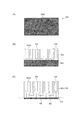
最初に、図1〜図4を参照しながら本発明の実施例1を説明する。図(A)は本実施例のコンデンサの断面図,図1(B)はコンデンサ素子の容量発生部を一部破断して示す外観斜視図である。図2〜図4は、本実施例の製造工程の一例を示す図である。本実施例のコンデンサ10は、図1(A)に示すように、コンデンサ素子12を中心に構成されている。コンデンサ素子12は、容量発生部(ないし内部電極充填領域)14と、その両側に形成された捨て部(ないし内部電極非充填領域)16A及び16Bからなり、前記容量発生部14は、図1(B)に示すように、誘電体層18と、該誘電体層18中に略円柱状に形成された複数の第1の内部電極20及び第2の内部電極22を含んでいる。また、前記コンデンサ素子12は、一方の主面側に形成された前記第1の内部電極20と導通する第1の外部電極24,該第1の外部電極24上に形成された絶縁層28,該絶縁層28上に形成されており前記第2の内部電極22と導通する第2の外部電極32を備えている。前記第1の外部電極24と第2の内部電極22の間には、前記絶縁層28が入り込んでおり、該絶縁層28によって第1の外部電極24と第2の内部電極22の絶縁が図られている。
First,
このようなコンデンサ素子12の外側には、保護層34が設けられている。該保護層34には、前記第1の外部電極24の一部が露出する露出部36と、第2の外部電極32の一部が露出する露出部38が形成されている。そして、前記露出部36及び38に導通するように、端子電極40,42がコンデンサ素子12の両側面に形成されている。前記第1の内部電極20及び第2の内部電極22は、縦横比が大きく(すなわち、アスペクト比(AR)が高く)なっており、図1(B)に示すように、ランダム配置となっている。本実施例では、前記第1の内部電極20を正極,第2の内部電極22を負極に振り分けているが、逆であってもよい。
A
前記誘電体層18を形成する材料としては、弁金属(Al,Ta,Nb,Ti,Zr,Hf,Zn,W,Sbなど)の酸化物が用いられる。また、第1の内部電極20,第2の内部電極22としては、メッキ可能な金属全般(Cu,Ni,Co,Cr,Ag,Au,Pd,Fe,Sn,Pb,Ptなど)やこれらの合金などが用いられる。前記第1の外部電極24及び第2の外部電極32としては、金属全般(Cu,Ni,Cr,Ag,Au,Pd,Fe,Sn,Pb,Pt,Ir,Rh,Ru,Alなど)が用いられる。また、前記保護層34としては、例えば、SiO2,SiN,樹脂,金属酸化物などの絶縁体が用いられる。前記端子電極40,42としては、例えば、Cu,Ni,Au,半田などや、これらを積層したものなどが用いられる。
As a material for forming the
また、前記容量発生部14の各部の寸法の一例を示すと、第1の外部電極24及び第2の外部電極32の厚さが数10nm〜数μm,第1の内部電極20及び第2の内部電極22の径が数10nm〜数100nm,これら内部電極20及び22の長さが数100nm〜数100μmである。また、隣接する内部電極間の間隔は、数10nm〜数100nm,内部電極と外部電極間の間隔(すなわち絶縁層28の厚み)が数10nm〜数10μm,誘電体層18の厚さが数100nm〜数100μmである。また、保護層34は、数10nm〜数10μm程度の厚さに形成されている。
An example of the dimensions of each part of the
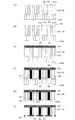
次に、図2〜図4も参照して、本実施例の製造方法を説明する。なお、図2〜図4には、コンデンサ素子12の容量発生部14に相当する部分のみが図示されているが、実際には、その両側に前記捨て部16A,16Bに相当する部分が形成されるものとする。まず、図2(A)に示すように、上述した弁金属からなる金属基材50を用意する。そして、必要に応じて、該金属基材50の表面50Aに、陽極酸化の基点となるピット(図示せず)を、最密充填六方配列で形成する。次に、電圧を印加して陽極酸化処理を施すことにより、図2(B)に示すように、一方の主面52A側で開口した所望の深さ(ないし長さ)の第1の孔54を、酸化物基材52の厚み方向に形成する。引き続き、前記第1の孔54を形成したときよりも大きな印加電圧で陽極酸化を施し、図2(C)に示すように、酸化物基材52に第2の孔56を形成する。陽極酸化で発生する孔のピッチ(孔同士の間隔)は電圧に比例するため、大きい電圧で処理された第2の孔56はピッチが大きくなり、前の工程で形成された第1の孔54の一部とランダムに接続される。本実施例では、前記酸化物基材52が誘電体層18として用いられる。
Next, the manufacturing method of a present Example is demonstrated with reference also to FIGS. 2 to 4 show only a portion corresponding to the
前記陽極酸化処理の条件は、図2(B)に示す1段階目の陽極酸化の印加電圧を数V〜数100V,処理時間を数分〜数日とする。図2(C)に示す2段階目の陽極酸化では、電圧値を1段階目の数倍とし、処理時間を数分〜数十分とする。例えば、1段階目の印加電圧を40Vとすることによりピッチが約100nmの第1の孔54が得られ、2段階目の印加電圧を80Vとすることによりピッチが約200nmの第2の孔56が得られる。2段階目の電圧値を上述した範囲内とすることにより、第2の孔56に接続された第1の孔54と、接続されていない第1の孔54の数を概ね同等とすることができる。これにより、前記第2の孔56に接続された第1の孔54の内側に形成される第1の内部電極20と、第2の孔56に接続されていない第1の孔54の内側に形成される第2の内部電極22の割合が同等となるため、効率的に容量を取り出すことが可能となる。また、前記2段階目の処理時間を上述の範囲内とすることで、孔のピッチ変換が十分に完了しつつ、2段階目で形成される酸化物基材の厚さを小さくすることができる。該2段階目で形成される酸化物基材は、後の工程で除去されるため、できるだけ薄いことが好ましいため都合がよい。
The conditions of the anodizing treatment are such that the applied voltage of the first stage anodizing shown in FIG. 2B is several volts to several hundred volts and the treatment time is several minutes to several days. In the second stage anodic oxidation shown in FIG. 2C, the voltage value is several times the first stage, and the treatment time is several minutes to several tens of minutes. For example, a
次に、前記図2(C)に示す状態から、同図に点線で示す位置で金属基材50の地金部分を除去するとともに、図3(A)に点線で示すように、前記第2の孔56の底面を、前記酸化物基材52の他方の主面52Bにおいて開口する(図3(B))。同工程の開口は、例えば、燐酸を用いたウェットエッチングや塩素系ガスを用いたドライエッチングなどの手法により行われる。そして、図3(C)に示すように、酸化物基材52の主面52Aに、PVDなどの適宜手法により、導電体からなるシード層58を形成する。次に、図3(D)に示すように、前記シード層58をシードとして前記第2の孔56と接続された第1の孔54の内側に電極材料であるメッキ導体を埋め込み、第1の内部電極20を形成する。このとき、前記第2の孔56に接続されていない第1の孔54の底部は開口していないため、前記メッキ導体が埋め込まれることがない。なお、前記メッキ導体は、第前記第1の孔54の端部近傍まで埋め込まれる。
Next, from the state shown in FIG. 2 (C), the
次に、図3(D)に点線で示す位置で酸化物基材52を切除し、図3(E)に示すように、前記第1の内部電極20の端部20Aを露出させるとともに、前記第1の内部電極20が形成されていない第1の孔54の底部を開口させる。ここでは、CMPスラリー砥粒の孔内への侵入を回避するため、固定砥粒CMP工法が好ましい。そして、図3(F)に示すように、前記酸化物基材52の主面52Bに、第1の外部電極24を形成する。該第1の外部電極24は、前記図3(E)で開口した第1の孔54に対応する位置に開口部26を有するとともに、前記第1の内部電極20の露出した端部20Aと導通する。前記第1の外部電極24は、開口した第1の孔54を塞がずに酸化物基材主面52Bのみに成膜することが必要であるため、PVD(蒸着やスパッタなど)による異方的な膜成長方法により、膜厚を薄く形成することが好ましい。次に、図4(A)に示すように、前記開口部26を、前記図3(E)で開口した第1の孔54の径よりも大きく、かつ、前記第1の内部電極20に達しないように拡張する。これは、後述する工程で形成する第2の内部電極22と前記第1の外部電極24の絶縁を図るためである。該工程においては、隣接する第1の内部電極20上の第1の外部電極24を残す必要があるため、等方的でマイルドなウェットエッチング処理が好ましい。
Next, the
続いて、図4(B)に示すように、前記第1の外部電極24上に絶縁層28を形成する。該絶縁層28は、前記第1の外部電極24上及びその側面に、前記第1の外部電極24の成膜方法と同様の手法により形成される。次に、前記図3(E)で開口した第1の孔54に、前記第1の外部電極24を超える深さ(長さ)となるように、電極材料であるメッキ導体を埋め込み、第2の内部電極22を形成する。
Subsequently, as shown in FIG. 4B, an insulating
そして、図4(C)に点線で示す位置で、前記絶縁層28を切除し、図4(D)に示すように前記第2の内部電極22の端部22Aを露出させる。次に、図4(E)に示すように前記シード層58を除去する。そして、図4(F)に示すように、前記図4(D)で露出させた第2の内部電極22の端部22Aと導通する第2の外部電極32を、前記絶縁層28上の全面に形成することにより、コンデンサ素子12が得られる。その後、前記保護層34や、端子電極40及び42を適宜手法で設けると、図1(A)に示すコンデンサ10が得られる。このようにして得られたコンデンサ10では、正負それぞれの内部電極20,22を流れる電流の方向が反対となり、磁界相殺効果によってESLが低減される。
Then, the insulating
このように、実施例1によれば、弁金属を陽極酸化して得られた多孔質の酸化物基材52を誘電体層18として利用し、その孔内に円柱状に形成された複数の第1の内部電極20及び第2の内部電極22をそれぞれ取出す外部電極24,32を、前記誘電体層18の同一主面側に平行に形成する構成としたので、次のような効果がある。
(1)第1の内部電極20及び第2の内部電極22を流れる電流の方向が反対となるため、磁界相殺効果によってESLが低減され、高周波特性の向上を図ることができる。
(2)第1の内部電極20及び第2の内部電極22を略円柱状とし、導電体の対向面積を大きくすることとしたので、高容量化を図ることができる。
(3)ナノスケールパターン形成が不要であり、製造プロセスの簡略及び低コスト化を図ることができる。
Thus, according to Example 1, the porous
(1) Since the directions of the currents flowing through the first
(2) Since the first
(3) Nanoscale pattern formation is unnecessary, and the manufacturing process can be simplified and the cost can be reduced.
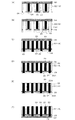
次に、図5を参照しながら本発明の実施例2を説明する。なお、上述した実施例1と同一ないし対応する構成要素には同一の符号を用いることとする。図5は、本実施例のコンデンサ素子60の製造工程の一例を示す斜視図である。前記実施例1のコンデンサ素子12では、誘電体層18として弁金属の酸化物のみが適用可能であるが、本実施例は、誘電体層の材料の選択性の幅の向上を図るためのものである。本実施例のコンデンサ素子60は、図5(C)に示すように、誘電体層62中に、前記実施例1と同様に複数の円柱状の第1の内部電極20及び第2の内部電極22が形成されており、それぞれ、誘電体層62の一方の主面側に形成された第1の外部電極24及び第2の外部電極32に接続されている。コンデンサ素子60を構成する各部の寸法は、実施例1と同様である。また、内部電極20及び22,外部電極24及び32,絶縁層28,保護層34,端子電極40及び42の材料は、上述した実施例1と同様のものが用いられる。一方、本実施例では、前記誘電体層62を形成する材料としては、上述した実施例1で用いた弁金属(Al,Ta,Nb,Ti,Zr,Hf,Zn,W,Sbなど)の酸化物のほか、複合酸化物(BaTiO3,SrTiO3などのペロブスカイト酸化物など)や樹脂が利用可能である。
Next, Embodiment 2 of the present invention will be described with reference to FIG. In addition, the same code | symbol shall be used for the component which is the same as that of Example 1 mentioned above, or respond | corresponds. FIG. 5 is a perspective view showing an example of the manufacturing process of the
本実施例のコンデンサ素子60の製造方法は、金属基材の陽極酸化処理を2段階で行ってから第2の外部電極32を形成するまでの工程は、上述した実施例1と同様である。図5(A)に示すように、第2の外部電極32を形成したのち、図5(B)に示すように酸化物基材52からなる誘電体層18を選択的に溶解除去して第1の内部電極20及び第2の内部電極22を露出させる。例えば、電極材料がNiであり、酸化物基材52がAl2O3の場合は、NaOHが選択除去に有効である。そして、空隙部64に他の誘電体材料を充填して、図5(C)に示す誘電体層62を形成する。内部電極20及び22のアスペクト比が大きいため、埋め込み性やデポレートを考慮すると、前記他の誘電体材料の充填手法は、塗布やディピング等のウェット手法が好ましい。前記他の誘電体材料は、コンデンサ素子60の用途に応じて選択が可能であるが、弁金属の酸化物を利用する場合には、除去した酸化物基材52よりも誘電率が高い酸化物を充填すると、より大きな容量値を得ることができ、素子の信頼性の向上を図ることができる。このように、実施例2によれば、上述した実施例1の効果に加え、誘電体層62を形成する材料の選択性が向上するという効果が得られる。
In the method of manufacturing the
なお、本発明は、上述した実施例に限定されるものではなく、本発明の要旨を逸脱しない範囲内において種々変更を加え得ることができる。例えば、以下のものも含まれる。
(1)前記実施例で示した形状,寸法は一例であり、必要に応じて適宜変更してよい。
(2)材料についても同様に、公知の各種の材料を利用してよい。例えば、前記実施例1では、誘電体層18を形成するための金属基材の具体例としてアルミニウムを挙げたが、陽極酸化が可能な金属であれば、公知の各種の金属が適用可能である。
(3)前記実施例1で示した電極引出構造も一例であり、同様の効果を奏するように適宜設計変更可能である。実施例2についても同様である。
In addition, this invention is not limited to the Example mentioned above, A various change can be added in the range which does not deviate from the summary of this invention. For example, the following are also included.
(1) The shapes and dimensions shown in the above embodiments are examples, and may be appropriately changed as necessary.
(2) Similarly, various known materials may be used for the material. For example, in the first embodiment, aluminum is given as a specific example of the metal base material for forming the
(3) The electrode lead-out structure shown in the first embodiment is also an example, and the design can be changed as appropriate so as to achieve the same effect. The same applies to the second embodiment.
本発明によれば、金属の陽極酸化により得られた多孔質誘電体を利用し、その孔内に円柱状に複数形成された正極及び負極の内部電極をそれぞれ取出す外部電極を、前記多孔質誘電体の同一主面側に平行に形成する構成とし、必要に応じて、前記多孔質誘電体を除去し、他の誘電体材料を充填する。これによって、ナノスケールのパターン形成を必要とせずに、容量密度の向上,製造プロセスの簡略化,高周波特性の向上(ESLの低減),誘電体材料の選択性の向上を図ることとしたので、コンデンサの用途に適用できる。特に、高周波向けコンデンサの用途に好適である。 According to the present invention, the porous dielectric obtained by anodic oxidation of metal is used, and external electrodes for taking out a plurality of positive and negative internal electrodes formed in a columnar shape in the holes are provided as the porous dielectric. The porous dielectric is removed and filled with another dielectric material, if necessary, so as to be formed parallel to the same main surface side of the body. As a result, it was decided to improve the capacitance density, simplify the manufacturing process, improve the high frequency characteristics (reduce ESL), and improve the selectivity of the dielectric material without requiring nanoscale pattern formation. Applicable to capacitor applications. In particular, it is suitable for high frequency capacitors.
10:コンデンサ
12:コンデンサ素子
14:容量発生部(内部電極充填領域)
16A,16B:捨て部(内部電極非充填領域)
18:誘電体層
20:第1の内部電極(正極)
20A:端部
22:第2の内部電極(負極)
22A:端部
24:第1の外部電極
26:開口部
28:絶縁層
32:第2の外部電極
34:保護層
36,38:露出部
40,42:端子電極
50:金属基材
50A:表面
52:酸化物基材
52A,52B:主面
54:第1の孔
56:第2の孔
58:シード層
60:コンデンサ素子
62:誘電体層
64:空隙部
10: Capacitor 12: Capacitor element 14: Capacitance generator (internal electrode filling region)
16A, 16B: Throwing part (internal electrode non-filling region)
18: Dielectric layer 20: First internal electrode (positive electrode)
20A: End 22: Second internal electrode (negative electrode)
22A: end 24: first external electrode 26: opening 28: insulating layer 32: second external electrode 34:
Claims (6)
前記正極及び負極の内部電極がランダムに配置されており、
前記コンデンサの一つの主面上に形成されており、前記孔内に形成された複数の一方極の内部電極と導通するとともに、複数の他方極の内部電極が絶縁状態で貫通する第1の外部電極層と、
該第1の外部電極層上に形成されており、前記他方極の内部電極が貫通する絶縁層と、
該絶縁層上に前記第1の外部電極層と平行に形成されており、前記他方極の内部電極と導通する第2の外部電極層と、
を備えたことを特徴とするコンデンサ。 A capacitor having a substantially rectangular parallelepiped shape or a substantially cubic shape, in which a plurality of positive and negative internal electrodes are respectively formed in a columnar shape in parallel in a hole of a porous dielectric obtained by anodizing a metal substrate. ,
The positive and negative internal electrodes are randomly arranged,
A first outer surface formed on one main surface of the capacitor and electrically connected to the plurality of one-pole internal electrodes formed in the hole and through which the plurality of other-pole internal electrodes penetrates in an insulated state. An electrode layer;
An insulating layer formed on the first external electrode layer, through which the internal electrode of the other electrode passes;
A second external electrode layer formed on the insulating layer in parallel with the first external electrode layer and electrically connected to the internal electrode of the other electrode;
A capacitor characterized by comprising.
前記金属の基材に電圧を印加して陽極酸化し、酸化物基材の一方の主面で開口するとともに、電極材料を充填するための所定の深さを有する略円柱状の第1の孔を、前記酸化物基材の厚み方向に複数形成する工程1,
前記金属基材を前記工程1よりも大きな印加電圧によって陽極酸化し、前記第1の孔よりもピッチが大きく、かつ、一部の前記第1の孔の先端と不規則に接続する第2の孔を複数形成する工程2,
残存する金属の基材を除去するとともに、前記第2の孔の底面を、前記酸化物基材の一方の主面と対向する他方の主面側で開口する工程3,
前記酸化物基材の一方の主面全体に、導電性のシード層を形成する工程4,
前記第2の孔に接続された第1の孔に電極材料を埋め込み、第1の内部電極を形成する工程5,
前記酸化物基材の他方の主面側を、前記第1の内部電極の端部を露出させ、かつ、該第1の内部電極が形成されていない第1の孔の底面を開口させる厚みで切除する工程6,
前記酸化物基材の他方の主面に、前記工程6で開口した第1の孔に対応する位置に開口部を有し、かつ、前記第1の内部電極の露出した端部と導通する第1の外部電極層を形成する工程7,
前記第1の外部電極層の開口部を、前記開口した第1の孔の径よりも大きく、かつ、前記第1の外部電極層と導通した第1の内部電極に達しない寸法に拡張する工程8,
該工程8で開口部が拡張された第1の外部電極層上及びその側面に、絶縁層を形成する工程9,
前記開口した第1の孔に、前記第1の外部電極層を超える深さとなるように電極材料を埋め込み、前記第1の孔と略同一の径を有する第2の内部電極を形成する工程10,
前記絶縁層を切除し、前記第2の内部電極の端部を露出する工程11,
前記シード層を除去するとともに、露出した前記第2の内部電極の端部と導通する第2の外部電極層を、前記絶縁層上に形成する工程12,
を含むことを特徴とするコンデンサの製造方法。 A method for producing a capacitor using a porous oxide substrate obtained by anodizing a metal substrate,
A substantially cylindrical first hole having a predetermined depth for filling the electrode material while applying an electric voltage to the metal base material, anodizing it, opening at one main surface of the oxide base material Forming a plurality of oxides in the thickness direction of the oxide substrate 1,
The metal substrate is anodized by an applied voltage larger than that in the step 1, and the pitch is larger than that of the first holes, and the second is connected irregularly to the tips of some of the first holes. Step 2 for forming a plurality of holes
Removing the remaining metal base material, and opening the bottom surface of the second hole on the other main surface side opposite to one main surface of the oxide base material;
Forming a conductive seed layer on one main surface of the oxide substrate;
A step of burying an electrode material in the first hole connected to the second hole to form a first internal electrode;
The thickness of the other main surface side of the oxide base is such that the end portion of the first internal electrode is exposed and the bottom surface of the first hole in which the first internal electrode is not formed is opened. Cutting process 6,
The second main surface of the oxide base material has an opening at a position corresponding to the first hole opened in the step 6 and is electrically connected to the exposed end of the first internal electrode. Forming an external electrode layer 1, 7;
Expanding the opening of the first external electrode layer to a size that is larger than the diameter of the opened first hole and does not reach the first internal electrode that is in conduction with the first external electrode layer; 8,
Forming an insulating layer on the first external electrode layer whose opening is expanded in step 8 and on its side surface,
Step 10 of embedding an electrode material in the opened first hole so as to have a depth exceeding the first external electrode layer, thereby forming a second internal electrode having substantially the same diameter as the first hole. ,
Removing the insulating layer and exposing an end of the second internal electrode;
Removing the seed layer and forming a second external electrode layer on the insulating layer, the conductive layer being electrically connected to the exposed end of the second internal electrode;
A method for producing a capacitor, comprising:
該工程13によって前記第1及び第2の内部電極間に生じた空隙部に、除去した酸化物基材とは異なる誘電体材料を充填する工程14,
を含むことを特徴とする請求項3記載のコンデンサの製造方法。 After the step 12, the step 13 of removing the oxide base material,
Filling the gap formed between the first and second internal electrodes in the step 13 with a dielectric material different from the removed oxide substrate;
The method of manufacturing a capacitor according to claim 3, comprising:
Priority Applications (3)
| Application Number | Priority Date | Filing Date | Title |
|---|---|---|---|
| JP2010041129A JP5432002B2 (en) | 2010-02-25 | 2010-02-25 | Capacitor and manufacturing method thereof |
| PCT/JP2011/053626 WO2011105312A1 (en) | 2010-02-25 | 2011-02-21 | Capacitor and method of manufacturing thereof |
| US13/594,517 US8767374B2 (en) | 2010-02-25 | 2012-08-24 | Capacitors and method for manufacturing the same |
Applications Claiming Priority (1)
| Application Number | Priority Date | Filing Date | Title |
|---|---|---|---|
| JP2010041129A JP5432002B2 (en) | 2010-02-25 | 2010-02-25 | Capacitor and manufacturing method thereof |
Publications (3)
| Publication Number | Publication Date |
|---|---|
| JP2011176245A JP2011176245A (en) | 2011-09-08 |
| JP2011176245A5 JP2011176245A5 (en) | 2013-06-06 |
| JP5432002B2 true JP5432002B2 (en) | 2014-03-05 |
Family
ID=44506720
Family Applications (1)
| Application Number | Title | Priority Date | Filing Date |
|---|---|---|---|
| JP2010041129A Active JP5432002B2 (en) | 2010-02-25 | 2010-02-25 | Capacitor and manufacturing method thereof |
Country Status (3)
| Country | Link |
|---|---|
| US (1) | US8767374B2 (en) |
| JP (1) | JP5432002B2 (en) |
| WO (1) | WO2011105312A1 (en) |
Families Citing this family (13)
| Publication number | Priority date | Publication date | Assignee | Title |
|---|---|---|---|---|
| JP5904765B2 (en) * | 2011-11-10 | 2016-04-20 | 太陽誘電株式会社 | Capacitor and manufacturing method thereof |
| JP6097540B2 (en) * | 2012-01-17 | 2017-03-15 | ローム株式会社 | Chip capacitor and manufacturing method thereof |
| KR20140138701A (en) * | 2012-03-22 | 2014-12-04 | 캘리포니아 인스티튜트 오브 테크놀로지 | Micro -and nanoscale capacitors that incorporate an array of conductive elements having elongated bodies |
| JP2014011419A (en) * | 2012-07-03 | 2014-01-20 | Taiyo Yuden Co Ltd | Capacitor |
| JP6218558B2 (en) * | 2013-10-30 | 2017-10-25 | 太陽誘電株式会社 | Capacitor |
| JP6343529B2 (en) * | 2014-09-11 | 2018-06-13 | 太陽誘電株式会社 | Electronic components, circuit modules and electronic equipment |
| US10313090B2 (en) * | 2015-04-20 | 2019-06-04 | Apple Inc. | Tone mapping signaling in a preamble |
| US10476639B2 (en) | 2015-05-05 | 2019-11-12 | Apple Inc. | User assignment of resource blocks in a preamble |
| US10431508B2 (en) | 2015-07-19 | 2019-10-01 | Vq Research, Inc. | Methods and systems to improve printed electrical components and for integration in circuits |
| US10242803B2 (en) * | 2015-07-19 | 2019-03-26 | Vq Research, Inc. | Methods and systems for geometric optimization of multilayer ceramic capacitors |
| US10607779B2 (en) * | 2016-04-22 | 2020-03-31 | Rohm Co., Ltd. | Chip capacitor having capacitor region directly below external electrode |
| KR102460748B1 (en) * | 2017-09-21 | 2022-10-31 | 삼성전기주식회사 | Capacitor Component |
| FR3120982A1 (en) * | 2021-03-18 | 2022-09-23 | Commissariat A L'energie Atomique Et Aux Energies Alternatives | HIGH DENSITY CAPACITIVE DEVICE AND METHOD FOR FABRICATING SUCH A DEVICE |
Family Cites Families (15)
| Publication number | Priority date | Publication date | Assignee | Title |
|---|---|---|---|---|
| JPS5577127A (en) * | 1978-12-06 | 1980-06-10 | Murata Manufacturing Co | Grain boundary insulating semiconductor porcelain capacitor |
| JPH11204372A (en) * | 1997-11-14 | 1999-07-30 | Murata Mfg Co Ltd | Monolithic capacitor |
| EP0917165B1 (en) | 1997-11-14 | 2007-04-11 | Murata Manufacturing Co., Ltd. | Multilayer capacitor |
| JP2001189234A (en) * | 1999-12-28 | 2001-07-10 | Tdk Corp | Multilayer capacitors |
| US8064188B2 (en) * | 2000-07-20 | 2011-11-22 | Paratek Microwave, Inc. | Optimized thin film capacitors |
| JP2003249417A (en) * | 2002-02-25 | 2003-09-05 | Tdk Corp | Capacitor structure and manufacturing method of the same |
| KR100534845B1 (en) * | 2003-12-30 | 2005-12-08 | 현대자동차주식회사 | Method for Manufacturing Nano-structured Electrode of Metal Oxide |
| KR100649579B1 (en) * | 2004-12-07 | 2006-11-28 | 삼성전기주식회사 | Stacked Capacitors and Stacked Capacitor Arrays |
| US7557013B2 (en) * | 2006-04-10 | 2009-07-07 | Micron Technology, Inc. | Methods of forming a plurality of capacitors |
| US8385046B2 (en) * | 2006-11-01 | 2013-02-26 | The Arizona Board Regents | Nano scale digitated capacitor |
| JP4357577B2 (en) | 2007-06-14 | 2009-11-04 | 太陽誘電株式会社 | Capacitor and manufacturing method thereof |
| JP4382841B2 (en) | 2007-08-20 | 2009-12-16 | 太陽誘電株式会社 | Capacitor and manufacturing method thereof |
| JP5270124B2 (en) * | 2007-09-03 | 2013-08-21 | ローム株式会社 | Capacitors and electronic components |
| JP4493686B2 (en) * | 2007-09-27 | 2010-06-30 | 太陽誘電株式会社 | Capacitor and manufacturing method thereof |
| JP2010033939A (en) * | 2008-07-30 | 2010-02-12 | Murata Mfg Co Ltd | Ion conductive membrane, manufacturing method for ion conductive membrane, fuel cell, and hydrogen sensor |
-
2010
- 2010-02-25 JP JP2010041129A patent/JP5432002B2/en active Active
-
2011
- 2011-02-21 WO PCT/JP2011/053626 patent/WO2011105312A1/en not_active Ceased
-
2012
- 2012-08-24 US US13/594,517 patent/US8767374B2/en active Active
Also Published As
| Publication number | Publication date |
|---|---|
| JP2011176245A (en) | 2011-09-08 |
| WO2011105312A1 (en) | 2011-09-01 |
| US8767374B2 (en) | 2014-07-01 |
| US20130083454A1 (en) | 2013-04-04 |
Similar Documents
| Publication | Publication Date | Title |
|---|---|---|
| JP5432002B2 (en) | Capacitor and manufacturing method thereof | |
| JP4493686B2 (en) | Capacitor and manufacturing method thereof | |
| JP4907594B2 (en) | Capacitor and manufacturing method thereof | |
| JP4382841B2 (en) | Capacitor and manufacturing method thereof | |
| TWI607463B (en) | Capacitor and capacitor manufacturing method | |
| JP4357577B2 (en) | Capacitor and manufacturing method thereof | |
| CN105706234A (en) | Structure with an improved capacitor | |
| JP5416840B2 (en) | Capacitor and manufacturing method thereof | |
| WO2015118902A1 (en) | Capacitor | |
| JP6043548B2 (en) | Capacitor | |
| JP6343529B2 (en) | Electronic components, circuit modules and electronic equipment | |
| JP2014011419A (en) | Capacitor | |
| JP6218558B2 (en) | Capacitor | |
| KR101555481B1 (en) | Capacitor and method of manufacturing the same | |
| JP6218660B2 (en) | Capacitor | |
| WO2017026294A1 (en) | Capacitor and capacitor production method | |
| WO2018021115A1 (en) | Capacitor and method for producing capacitor | |
| JP2016004827A (en) | Capacitor, circuit module, and mobile communication equipment |
Legal Events
| Date | Code | Title | Description |
|---|---|---|---|
| A621 | Written request for application examination |
Free format text: JAPANESE INTERMEDIATE CODE: A621 Effective date: 20130123 |
|
| A521 | Request for written amendment filed |
Free format text: JAPANESE INTERMEDIATE CODE: A523 Effective date: 20130418 |
|
| A131 | Notification of reasons for refusal |
Free format text: JAPANESE INTERMEDIATE CODE: A131 Effective date: 20130827 |
|
| A521 | Request for written amendment filed |
Free format text: JAPANESE INTERMEDIATE CODE: A523 Effective date: 20131015 |
|
| TRDD | Decision of grant or rejection written | ||
| A01 | Written decision to grant a patent or to grant a registration (utility model) |
Free format text: JAPANESE INTERMEDIATE CODE: A01 Effective date: 20131112 |
|
| A61 | First payment of annual fees (during grant procedure) |
Free format text: JAPANESE INTERMEDIATE CODE: A61 Effective date: 20131205 |
|
| R150 | Certificate of patent or registration of utility model |
Free format text: JAPANESE INTERMEDIATE CODE: R150 Ref document number: 5432002 Country of ref document: JP Free format text: JAPANESE INTERMEDIATE CODE: R150 |
|
| R250 | Receipt of annual fees |
Free format text: JAPANESE INTERMEDIATE CODE: R250 |
|
| R250 | Receipt of annual fees |
Free format text: JAPANESE INTERMEDIATE CODE: R250 |
|
| R250 | Receipt of annual fees |
Free format text: JAPANESE INTERMEDIATE CODE: R250 |
|
| R250 | Receipt of annual fees |
Free format text: JAPANESE INTERMEDIATE CODE: R250 |
|
| R250 | Receipt of annual fees |
Free format text: JAPANESE INTERMEDIATE CODE: R250 |
|
| R250 | Receipt of annual fees |
Free format text: JAPANESE INTERMEDIATE CODE: R250 |
|
| R250 | Receipt of annual fees |
Free format text: JAPANESE INTERMEDIATE CODE: R250 |
|
| R250 | Receipt of annual fees |
Free format text: JAPANESE INTERMEDIATE CODE: R250 |
|
| R250 | Receipt of annual fees |
Free format text: JAPANESE INTERMEDIATE CODE: R250 |
|
| R250 | Receipt of annual fees |
Free format text: JAPANESE INTERMEDIATE CODE: R250 |