JP6037300B2 - Circuit member joint structure - Google Patents
Circuit member joint structure Download PDFInfo
- Publication number
- JP6037300B2 JP6037300B2 JP2012059175A JP2012059175A JP6037300B2 JP 6037300 B2 JP6037300 B2 JP 6037300B2 JP 2012059175 A JP2012059175 A JP 2012059175A JP 2012059175 A JP2012059175 A JP 2012059175A JP 6037300 B2 JP6037300 B2 JP 6037300B2
- Authority
- JP
- Japan
- Prior art keywords
- circuit member
- metal
- solder
- electrode
- region
- Prior art date
- Legal status (The legal status is an assumption and is not a legal conclusion. Google has not performed a legal analysis and makes no representation as to the accuracy of the status listed.)
- Active
Links
Images


Classifications
-
- H—ELECTRICITY
- H01—ELECTRIC ELEMENTS
- H01L—SEMICONDUCTOR DEVICES NOT COVERED BY CLASS H10
- H01L2224/00—Indexing scheme for arrangements for connecting or disconnecting semiconductor or solid-state bodies and methods related thereto as covered by H01L24/00
- H01L2224/73—Means for bonding being of different types provided for in two or more of groups H01L2224/10, H01L2224/18, H01L2224/26, H01L2224/34, H01L2224/42, H01L2224/50, H01L2224/63, H01L2224/71
- H01L2224/732—Location after the connecting process
- H01L2224/73201—Location after the connecting process on the same surface
- H01L2224/73203—Bump and layer connectors
- H01L2224/73204—Bump and layer connectors the bump connector being embedded into the layer connector
-
- H—ELECTRICITY
- H01—ELECTRIC ELEMENTS
- H01L—SEMICONDUCTOR DEVICES NOT COVERED BY CLASS H10
- H01L2224/00—Indexing scheme for arrangements for connecting or disconnecting semiconductor or solid-state bodies and methods related thereto as covered by H01L24/00
- H01L2224/80—Methods for connecting semiconductor or other solid state bodies using means for bonding being attached to, or being formed on, the surface to be connected
- H01L2224/83—Methods for connecting semiconductor or other solid state bodies using means for bonding being attached to, or being formed on, the surface to be connected using a layer connector
- H01L2224/8319—Arrangement of the layer connectors prior to mounting
- H01L2224/83192—Arrangement of the layer connectors prior to mounting wherein the layer connectors are disposed only on another item or body to be connected to the semiconductor or solid-state body
Landscapes
- Electric Connection Of Electric Components To Printed Circuits (AREA)
- Structures For Mounting Electric Components On Printed Circuit Boards (AREA)
- Wire Bonding (AREA)
Description
本発明は、回路部材接合構造体に関する。さらに詳しくは、基板の電極と電子部品の電極、基板の電極同士、および電子部品の電極同士等を互いに接合した回路部材接合構造体に関する。 The present invention relates to a circuit member bonding structure. More specifically, the present invention relates to a circuit member bonding structure in which electrodes of a substrate and electrodes of an electronic component, electrodes of a substrate, electrodes of an electronic component, and the like are bonded to each other.
例えばプリント基板に電子部品を実装する場合のはんだ付けの工業的方法には、大きく分けて2つの方法がある。1つは、はんだをあらかじめ溶融してから、いずれかの電極に付着させるフロー方式であり、他の1つは、電極間にはんだを供給してから、はんだを加熱して溶融させるリフロー方式である。電子部品の小型化および高密度実装化の進展に伴って、リフロー方式が現在は主流となり、改良が行われている。 For example, there are two general methods of soldering when mounting electronic components on a printed circuit board. One is a flow method in which the solder is melted in advance and then adhered to one of the electrodes, and the other is a reflow method in which the solder is heated between the electrodes and then melted by heating. is there. With the progress of miniaturization and high-density mounting of electronic components, the reflow method is now mainstream and is being improved.
リフロー方式による接合方法の1つとして、熱硬化性樹脂等からなる接着剤に粒子状のはんだを混合し、その混合物を、接合される各電極の間と、プリント基板と電子部品本体との間に供給する方法についての研究および実用化が進んでいる(特許文献1および2参照)。この方法によれば、電極同士の接合と、プリント基板と電子部品本体との接合とを同時に行うことが可能となり、生産効率の向上が図れる。
As one of the joining methods by the reflow method, particulate solder is mixed with an adhesive made of a thermosetting resin and the mixture is mixed between each electrode to be joined and between the printed circuit board and the electronic component body. Research and practical application of a method for supplying the water to the liquid is progressing (see
そして、リフロー方式による電子部品の基板実装等においては、電子部品等が受ける熱ダメージを軽減するために、融点の低いはんだが使用されることが多い。 In the reflow method of mounting electronic components on a substrate, solder having a low melting point is often used in order to reduce thermal damage to the electronic components.
また、比較的小さな基板に1または複数の電子部品を実装してモジュール化した電子部品モジュールを、さらにマザーボード等の別の基板に実装することも一般的に行われる。この場合には、多段階のはんだ付け工程が実行されることになり、2段階目以降のはんだ付け工程も、リフロー方式で実行されることが多い。 In addition, it is generally performed that an electronic component module obtained by mounting one or a plurality of electronic components on a relatively small substrate to be modularized is further mounted on another substrate such as a mother board. In this case, a multi-step soldering process is executed, and the second and subsequent soldering processes are often executed by the reflow method.
ところが、2段階目以降のはんだ付け工程をリフロー方式で実行すると、それ以前のはんだ付け工程で形成されたはんだ接合部も一緒に加熱される。このため、再加熱されたはんだ接合部が溶融して、接続信頼性が低下したり、溶融はんだが、隣接する電極や配線と接触して、短絡が発生したりすることもあり得る。 However, when the second and subsequent soldering steps are executed by the reflow method, the solder joints formed in the previous soldering steps are also heated together. For this reason, the reheated solder joint may be melted and connection reliability may be lowered, or the molten solder may come into contact with adjacent electrodes or wirings, resulting in a short circuit.
このため、少なくとも、再加熱が予定されるはんだ接合部に対しては、高融点のはんだを使用することで、再溶融を防止することが好ましいといえる。ところが、そのような高融点のはんだを使用すると、はんだ付けの際に、より高温かつ長時間にわたって電子部品等を加熱する必要性が生じる。その結果、電子部品や基板に大きな熱ダメージが発生することが考えられる。さらに、はんだ付けに要する電力も大きくなるために、電子機器等の製造に要する電力量の増大を招く。 For this reason, it can be said that it is preferable to prevent remelting by using a high melting point solder at least for the solder joint portion where reheating is scheduled. However, when such a high-melting-point solder is used, it is necessary to heat an electronic component or the like at a higher temperature for a longer time during soldering. As a result, it is conceivable that large heat damage occurs in the electronic component or the substrate. Furthermore, since the electric power required for soldering also increases, the amount of electric power required for manufacturing electronic devices and the like is increased.
そこで、本発明は、各電極をはんだ付けするときの加熱温度を抑えることができるとともに、後ではんだ接合部が加熱されたときの再溶融を抑制することができる、回路部材接合構造体を提供することを目的とする。 Therefore, the present invention provides a circuit member joint structure that can suppress the heating temperature when soldering each electrode and can suppress remelting when the solder joint is heated later. The purpose is to do.
本発明の一局面は、第一接続用電極を有する第一回路部材と、前記第一接続用電極と対応する第二接続用電極を有する第二回路部材と、前記第一接続用電極と、前記第二接続用電極との間に介在し、前記第一接続用電極と、前記第二接続用電極とを電気的に接続するはんだ接合部と、を具備し、前記はんだ接合部が、金属部分を含み、前記金属部分は、第一金属元素を主成分として含む第一金属領域と、前記第一金属元素よりも融点の高い第二金属元素を主成分として含む第二金属領域と、を含み、前記第一金属領域は、前記はんだ接合部の外側で前記第一接続用電極と前記第二接続用電極とを接合し、前記第二金属領域は、前記はんだ接合部の中央側で前記第一接続用電極と前記第二接続用電極とを接合し、前記第一金属元素は前記二金属元素と合金を形成可能であり、かつ前記合金の融点は、前記第一金属領域の融点および前記第二金属領域の融点よりも低く、前記第一金属領域および前記第二金属領域は、いずれも前記合金の構成元素の偏析により生成した領域である、回路部材接合構造体に関する。 One aspect of the present invention includes a first circuit member having a first connection electrode, a second circuit member having a second connection electrode corresponding to the first connection electrode, the first connection electrode, A solder joint that is interposed between the second connection electrode and electrically connects the first connection electrode and the second connection electrode, wherein the solder joint is a metal A first metal region containing a first metal element as a main component, and a second metal region containing as a main component a second metal element having a melting point higher than that of the first metal element. The first metal region joins the first connection electrode and the second connection electrode outside the solder joint portion, and the second metal region is the center side of the solder joint portion. bonding the said the first connection electrode second connection electrode, wherein the first metal element said two metal It is capable of forming an element alloy, and melting point of the alloy, rather lower than the melting point of the melting point and the second metal region of the first metal region, wherein the first metal region and said second metal region, either The present invention also relates to a circuit member bonded structure, which is a region generated by segregation of constituent elements of the alloy .
上記回路部材接合構造体は、(i)第一電極を有する第一回路部材と、前記第一電極に対応する第二電極を有する第二回路部材と、熱硬化性樹脂を含むペーストとを準備する工程、ただし、前記第一電極、前記第二電極および前記ペーストの少なくとも一つが、はんだを含み、
(ii)前記第一電極および前記第二電極の少なくとも一方に、前記ペーストを供給する工程、
(iii)前記第一電極が前記第二電極に前記ペーストを介して着地するように、前記第一回路部材と前記第二回路部材とを近接配置する工程、
(iv)前記第一電極が前記第二電極に着地した状態で、少なくとも前記第一電極、前記第二電極および前記ペーストを含む接合領域を、前記はんだの融点以上の温度で、前記第一電極を前記第二電極に押圧しながら加熱して、前記はんだを溶融させるとともに、前記熱硬化性樹脂を硬化させる工程、
(v)前記接合領域を、前記はんだの融点以上の温度から徐冷する工程、を具備する、電極接合方法を適用することにより製造することができる。
The circuit member bonded structure includes (i) a first circuit member having a first electrode, a second circuit member having a second electrode corresponding to the first electrode, and a paste containing a thermosetting resin. A process wherein at least one of the first electrode, the second electrode, and the paste comprises solder,
(Ii) supplying the paste to at least one of the first electrode and the second electrode;
(Iii) placing the first circuit member and the second circuit member in proximity so that the first electrode lands on the second electrode via the paste;
(Iv) In a state where the first electrode is landed on the second electrode, a bonding region including at least the first electrode, the second electrode, and the paste is formed at a temperature equal to or higher than the melting point of the solder. Heating while pressing the second electrode to melt the solder and curing the thermosetting resin,
(V) The bonding region can be manufactured by applying an electrode bonding method including a step of gradually cooling the bonding region from a temperature equal to or higher than the melting point of the solder.
上記回路部材接合構造体は、第一電極を有する第一回路部材と、前記第一電極に対応する第二電極を有する第二回路部材とを、前記第一電極と前記第二電極との間に熱硬化性樹脂を含むペーストを介在させて接合する、前記第一電極、前記第二電極および前記ペーストの少なくとも一つが、はんだを含む、回路部材接合ラインであって、
前記第一電極および前記第二電極の少なくとも一方に、前記ペーストを供給するペースト供給装置と、
前記ペースト供給装置の下流に配置され、前記第一電極が前記第二電極に前記ペーストを介して着地するように、前記第一回路部材と前記第二回路部材とを近接配置するとともに、前記第一電極が前記第二電極に着地した状態で、少なくとも前記第一電極、前記第二電極および前記ペーストを含む接合領域を、前記はんだの融点以上の温度で加熱し、その後、徐冷することにより、前記熱硬化性樹脂を硬化させるとともに前記第一電極と前記第二電極とを接合する、実装ユニットと、を具備する、回路部材接合ラインにより製造することができる。
The circuit member bonded structure includes a first circuit member having a first electrode and a second circuit member having a second electrode corresponding to the first electrode, between the first electrode and the second electrode. A paste including a thermosetting resin is bonded to the first electrode, the second electrode, and at least one of the paste is a circuit member bonding line including solder,
A paste supply device for supplying the paste to at least one of the first electrode and the second electrode;
The first circuit member and the second circuit member are disposed close to each other so that the first electrode lands on the second electrode via the paste, and is disposed downstream of the paste supply device. In a state where one electrode is landed on the second electrode, at least the joining region including the first electrode, the second electrode, and the paste is heated at a temperature equal to or higher than the melting point of the solder, and then gradually cooled. And a mounting unit that cures the thermosetting resin and joins the first electrode and the second electrode to each other.
本発明によれば、溶融はんだを含む接合領域を徐冷することで、第一電極と第二電極とを接合するはんだ接合部が形成される。このとき、その徐冷の条件を、使用するはんだの組成に応じて適宜に設定することで、強度の低下を抑えつつ、より高融点のはんだ接合部を形成することが可能となる。したがって、各電極を、比較的低融点のはんだを使用して接合しても、高融点のはんだ接合部が形成される。その結果、各電極をはんだ付けするときの加熱温度を抑えることができるとともに、後ではんだ接合部が加熱されたときの再溶融を抑制することができる。 According to the present invention, a solder joint part that joins the first electrode and the second electrode is formed by slowly cooling the joint region containing the molten solder. At this time, by setting the slow cooling conditions appropriately according to the composition of the solder to be used, it becomes possible to form a solder joint having a higher melting point while suppressing a decrease in strength. Therefore, even if each electrode is joined using a relatively low melting point solder, a high melting point solder joint is formed. As a result, the heating temperature when soldering each electrode can be suppressed, and remelting when the solder joint is heated later can be suppressed.
本発明に係る電極接合方法は、第一回路部材の第一電極と、第二回路部材の第二電極とをはんだ付けにより接合する電極接合方法に関する。より具体的には、この接合方法においては、(i)第一電極を有する第一回路部材と、第一電極に対応する第二電極を有する第二回路部材と、熱硬化性樹脂を含むペーストとが準備される。ここで、接合に使用されるはんだは、第一電極に含まれていてもよいし、第二電極に含まれていてもよいし、上記のペーストに含まれていてもよい。 The electrode joining method according to the present invention relates to an electrode joining method for joining a first electrode of a first circuit member and a second electrode of a second circuit member by soldering. More specifically, in this joining method, (i) a first circuit member having a first electrode, a second circuit member having a second electrode corresponding to the first electrode, and a paste containing a thermosetting resin And are prepared. Here, the solder used for joining may be included in the first electrode, may be included in the second electrode, or may be included in the paste.
本接合方法は、さらに、(ii)第一電極および第二電極の少なくとも1方に、上記のペーストを供給する工程、(iii)第一電極が第二電極にペーストを介して着地するように、第一回路部材と第二回路部材とを近接配置する工程、(iv)第一電極が第二電極に着地した状態で、少なくとも第一電極、第二電極およびペーストを含む接合領域を、はんだの融点以上の温度で、第一電極を第二電極に押圧しながら加熱して、はんだを溶融させるとともに、熱硬化性樹脂を硬化させる工程、並びに、(v)その接合領域を、はんだの融点以上の温度から徐冷する工程、を含む。 The bonding method further includes (ii) supplying the paste to at least one of the first electrode and the second electrode, and (iii) so that the first electrode lands on the second electrode via the paste. A step of arranging the first circuit member and the second circuit member close to each other, (iv) in a state where the first electrode is landed on the second electrode, a bonding region including at least the first electrode, the second electrode and the paste is soldered Heating the first electrode against the second electrode at a temperature equal to or higher than the melting point of the solder to melt the solder and curing the thermosetting resin, and (v) the bonding area of the solder melting point A step of slow cooling from the above temperature.
上述した通り、本接合方法では、接合領域をはんだの融点以上の温度まで加熱することで、はんだが溶融する。その後、接合領域を冷却することで、溶融はんだが固化し、はんだ接合部が形成される。このとき、接合領域を徐冷することで、徐冷しない通常の場合に比べて、より融点の高いはんだ接合部を形成することが可能となる。 As described above, in this bonding method, the solder is melted by heating the bonding region to a temperature equal to or higher than the melting point of the solder. Thereafter, by cooling the joining region, the molten solder is solidified and a solder joint is formed. At this time, by gradually cooling the joining region, it becomes possible to form a solder joint having a higher melting point than in a normal case where the joining region is not gradually cooled.
その結果、比較的低融点のはんだを使用した場合にも、通常よりも高融点のはんだ接合部を形成できるので、特に高融点のはんだを使用する必要性がなくなる。その結果、リフロー方式ではんだ付けするときの第一回路部材および第二回路部材の加熱温度を低くすることができる。よって、各回路部材が大きな熱ダメージを受けるのを防止することができる。 As a result, even when a solder having a relatively low melting point is used, a solder joint having a higher melting point than usual can be formed, so that it is not necessary to use a solder having a particularly high melting point. As a result, the heating temperature of the first circuit member and the second circuit member when soldering by the reflow method can be lowered. Therefore, it is possible to prevent each circuit member from being greatly damaged by heat.
はんだは、いわゆるはんだバンプ、もしくは、はんだキャップとして第一電極および第二電極のいずれかに含ませることができる。または、はんだの微粒子を含むいわゆるクリームはんだを第一電極または第二電極に塗布することで、はんだを第一電極または第二電極のいずれかに含ませることができる。さらに、例えばはんだ接合部を封止するための、熱硬化性樹脂を含むペーストにはんだを含ませることで、電極間にはんだを供給し得る。 Solder can be included in either the first electrode or the second electrode as a so-called solder bump or solder cap. Alternatively, the solder can be included in either the first electrode or the second electrode by applying a so-called cream solder containing solder fine particles to the first electrode or the second electrode. Furthermore, for example, solder can be supplied between electrodes by including solder in a paste containing a thermosetting resin for sealing a solder joint.
なお、溶融はんだを含む接合領域を徐冷することで高融点のはんだ接合部を形成し得る理由は、必ずしも明らかではない。しかしながら、溶融はんだの冷却速度が偏析と関係することから、上記の理由は以下のように推測し得る。 The reason why a high melting point solder joint can be formed by slowly cooling the joint region containing the molten solder is not necessarily clear. However, since the cooling rate of the molten solder is related to segregation, the above reason can be estimated as follows.
一般に、はんだを溶融した後、冷却してはんだ接合部を形成すると、その接合部には、はんだに含まれる合金が偏析することが知られている。はんだ接合部の偏析が顕著になると、はんだ接合部の強度が低下すると考えられている。このため、偏析を抑えるように、一般的には、冷却ファン等の冷却装置を使用して、接合領域をできるだけ短い時間で冷却する運用が行われる。 In general, it is known that when a solder joint is formed by melting after melting the solder, an alloy contained in the solder is segregated at the joint. It is believed that when the segregation of the solder joint becomes significant, the strength of the solder joint decreases. For this reason, in order to suppress segregation, generally, an operation for cooling the joining region in as short a time as possible using a cooling device such as a cooling fan is performed.
これに対して、本発明者達は、接合領域を徐冷して合金を偏析させる場合でも、はんだ接合部の強度低下はそれほど問題にはならず、かつ、通常の場合よりも高融点のはんだ接合部を形成し得ることを見出した。その理由は、はんだ接合部に発生する偏析が適宜の程度であると、偏析による弊害(強度低下)が抑えられ、かつ、はんだ接合部の各領域の組成が通常の場合と異なることで、通常よりも融点の高いはんだ接合部を形成し得たものと考えられる。なお、本方法では、はんだ接合部による第一電極と第二電極との接合が、硬化樹脂により補強されるために、はんだ接合部自体の強度低下は、他の場合のようには大きな問題とはならない。 On the other hand, the inventors of the present invention do not pose a significant problem in strength reduction of the solder joint even when the alloy is segregated by gradually cooling the joint region, and a solder having a higher melting point than in a normal case. It has been found that joints can be formed. The reason for this is that if the segregation occurring in the solder joints is of an appropriate degree, the adverse effects (decrease in strength) due to segregation can be suppressed, and the composition of each region of the solder joints is different from the normal case. It is considered that a solder joint having a higher melting point could be formed. In this method, since the joining of the first electrode and the second electrode by the solder joint is reinforced by the cured resin, the strength reduction of the solder joint itself is a big problem as in other cases. Must not.
ここで、はんだが、第一融点を有する第一金属元素と、第一融点よりも高い第二融点を有する第二金属元素とを含むものとすれば、上記の接合領域の温度を、はんだの融点以上、かつ第二融点より低い所定温度以下の温度範囲TRに3〜60秒間留まらせるように、接合領域を徐冷するのが好ましい。これにより、より確実に、はんだ接合部の強度低下を抑えつつ、その高融点化を図ることができる。上記の時間範囲は、4.5〜40秒とするのがより好ましく、6〜20秒とするのがさらに好ましい。なお、上記の温度範囲TRは、はんだの融点以上、かつ第一融点より低い所定温度以下の温度範囲TRとするのがより好ましい。 Here, if the solder includes a first metal element having a first melting point and a second metal element having a second melting point higher than the first melting point, the temperature of the bonding region is set to It is preferable that the bonding region is gradually cooled so as to remain in a temperature range TR of not less than a melting point and not more than a predetermined temperature lower than the second melting point for 3 to 60 seconds. Thereby, it is possible to increase the melting point of the solder joint more reliably while suppressing the strength reduction of the solder joint. The above time range is more preferably 4.5 to 40 seconds, and further preferably 6 to 20 seconds. The temperature range TR is more preferably a temperature range TR that is not lower than a melting point of the solder and not higher than a predetermined temperature lower than the first melting point.
一方、上記の徐冷工程における接合領域の冷却速度は、0.1〜10℃/秒であるのが、はんだ接合部の強度低下を抑えながら、その高融点化を図る上で、より好ましい。接合領域の冷却速度は、0.5〜7℃/秒とするのがより好ましく、1〜4℃/秒とするのがさらに好ましい。なお、上記の冷却速度に関する条件は、少なくとも上記の温度範囲TRの平均の冷却速度について満足されていればよい。つまり、温度範囲TRにおいて、瞬間的に冷却速度が上記の範囲から外れてもよい。さらに、例えば、上記の温度範囲TRよりも高い温度領域では、平均的な冷却速度あるいは瞬間の冷却速度が上限(例えば10℃/秒)を超えていてもよいし、上記の温度範囲TRよりも低い温度領域では、平均的な冷却速度あるいは瞬間の冷却速度が下限(例えば0.1℃/秒)を下回っていてもよい。 On the other hand, the cooling rate of the joining region in the above-described slow cooling step is more preferably 0.1 to 10 ° C./second from the viewpoint of increasing the melting point while suppressing the strength reduction of the solder joint. The cooling rate of the joining region is more preferably 0.5 to 7 ° C./second, and further preferably 1 to 4 ° C./second. It should be noted that the above-described conditions relating to the cooling rate need only be satisfied for at least the average cooling rate in the temperature range TR. That is, in the temperature range TR, the cooling rate may instantaneously deviate from the above range. Further, for example, in a temperature range higher than the above temperature range TR, the average cooling rate or the instantaneous cooling rate may exceed an upper limit (for example, 10 ° C./second), or may be higher than the above temperature range TR. In the low temperature region, the average cooling rate or the instantaneous cooling rate may be lower than the lower limit (for example, 0.1 ° C./second).
ここで、第一金属元素がSnであり、第二金属元素がBiであるはんだ(以下、Sn−Bi系はんだという)は、低融点が容易に得られるので特に好ましい。このとき、上記の温度範囲TRを138〜200℃とすることで、より確実に、強度低下を抑えた、通常よりも高融点のはんだ接合部を実現し得る。なお、一般的なSn−Bi系はんだの融点は138℃であり、Snの融点は232℃であり、Biの融点は271℃である。したがって、SnとBiが偏析すると、はんだ接合部の耐熱性が向上する。 Here, a solder in which the first metal element is Sn and the second metal element is Bi (hereinafter referred to as Sn-Bi solder) is particularly preferable because a low melting point can be easily obtained. At this time, by setting the temperature range TR to 138 to 200 ° C., it is possible to more reliably realize a solder joint having a higher melting point than usual and suppressing a decrease in strength. Note that a general Sn—Bi solder has a melting point of 138 ° C., Sn has a melting point of 232 ° C., and Bi has a melting point of 271 ° C. Therefore, when Sn and Bi are segregated, the heat resistance of the solder joint is improved.
はんだを、熱硬化性樹脂のペーストに含ませる場合には、はんだの含有量は、4〜30質量%とするのが好ましい。熱硬化性樹脂は、特に限定されないが、エポキシ樹脂、フェノール樹脂、メラミン樹脂、ウレタン樹脂などを用いることができる。熱硬化性樹脂は、硬化剤、硬化促進剤などを含んでもよい。硬化剤としては、酸無水物、脂肪族または芳香族アミン、イミダゾールまたはその誘導体などが好ましく用いられ、硬化促進剤としては、ジシアンジアミドなどを例示できる。熱硬化性樹脂には、更に、反応性希釈剤、カーボンブラック、無機セラミックス粒子などの充填剤を含ませてもよい。熱硬化性樹脂の粘度は、例えば、反応性希釈剤や無機セラミックス粒子の含有量を変化させることにより制御してもよい。熱硬化性樹脂には、フラックスに含ませる活性剤などの成分を含ませてもよい。これにより、熱硬化性樹脂が回路部材の電極間に侵入しているような場合でも、溶融はんだと電極との濡れ性がより確実に確保される。 When the solder is included in the thermosetting resin paste, the content of the solder is preferably 4 to 30% by mass. Although a thermosetting resin is not specifically limited, An epoxy resin, a phenol resin, a melamine resin, a urethane resin etc. can be used. The thermosetting resin may contain a curing agent, a curing accelerator, and the like. As the curing agent, an acid anhydride, an aliphatic or aromatic amine, imidazole or a derivative thereof is preferably used, and examples of the curing accelerator include dicyandiamide. The thermosetting resin may further contain a filler such as a reactive diluent, carbon black, and inorganic ceramic particles. You may control the viscosity of a thermosetting resin by changing content of a reactive diluent or an inorganic ceramic particle, for example. Components such as an activator included in the flux may be included in the thermosetting resin. Thereby, even when the thermosetting resin penetrates between the electrodes of the circuit member, the wettability between the molten solder and the electrodes is more reliably ensured.
ここで、本発明に係る電極接合方法は、例えば少なくとも1つの第二回路部材に複数の第一回路部材を実装するときに、複数の第一回路部材の実装を、徐冷を含めて1つずつ完了する形態を取り得る。この場合には、上記工程(iii)、工程(iv)および工程(v)を含むフロー(X)は、少なくとも1つの第二回路部材に対して、複数の第一回路部材を、順次、近接配置し、第一回路部材毎に、接合領域を押圧しながら加熱し、徐冷するという工程により実行することができる。 Here, in the electrode joining method according to the present invention, for example, when mounting a plurality of first circuit members on at least one second circuit member, one mounting of the plurality of first circuit members including slow cooling is performed. Each form can be completed. In this case, the flow (X) including the step (iii), the step (iv), and the step (v) is performed by sequentially bringing a plurality of first circuit members close to at least one second circuit member. It arrange | positions and it can carry out by the process of heating and pressing down a joining area | region for every 1st circuit member.
他に、本発明に係る電極接合方法は、例えば少なくとも1つの第二回路部材に複数の第一回路部材を実装するときに、少なくとも1つの第二回路部材に対して複数の第一回路部材を順次に仮実装し、それにより形成されるはんだ接合部を一括して再加熱および徐冷する形態を取り得る。この場合には、上記工程(iii)と工程(iv)を含むフロー(Y)は、少なくとも1つの第二回路部材に対して、複数の第一回路部材を、順次、近接配置し、第一回路部材毎に接合領域を押圧しながら加熱する工程である。この加熱の後には、接合領域を急冷してもよい。一方、工程(v)は、フロー(Y)の後、複数の第一回路部材に対応する複数の接合領域を、同時に、はんだが溶融するまで再加熱し、徐冷する工程により実行することができる。これにより、第一回路部材の1個あたりの実装時間が短縮されるので、生産効率の向上が図れる。 In addition, in the electrode joining method according to the present invention, for example, when mounting a plurality of first circuit members on at least one second circuit member, a plurality of first circuit members are attached to at least one second circuit member. Temporary mounting can be performed sequentially, and the solder joints formed thereby can be reheated and gradually cooled. In this case, the flow (Y) including the step (iii) and the step (iv) includes a plurality of first circuit members arranged sequentially in proximity to at least one second circuit member. It is the process of heating while pressing the joining area for each circuit member. After this heating, the bonding region may be quenched. On the other hand, the step (v) may be performed by a step of reheating and gradually cooling the plurality of joining regions corresponding to the plurality of first circuit members after the flow (Y) until the solder is melted at the same time. it can. Thereby, since the mounting time per one 1st circuit member is shortened, the improvement of production efficiency can be aimed at.
さらに他に、本発明に係る電極接合方法は、例えば少なくとも1つの第二回路部材に複数の第一回路部材を実装するときに、全ての第一回路部材の実装を、徐冷を含めて一括して実行する形態を取り得る。この場合には、上記工程(iii)は、少なくとも1つの第二回路部材に対して、複数の第一回路部材を、順次、近接配置し、複数の第一回路部材の全てに対応する接合領域を形成する工程である。一方、工程(iv)と工程(v)を含むフロー(Z)は、複数の第一回路部材の全てに対応する接合領域を、同時に、押圧しながら加熱し、徐冷する工程である。これにより、さらに生産効率の向上が図れる。なお、上記の工程(iii)を複数の第二回路部材のそれぞれに対して繰り返し実行した後、上記のフロー(Z)を、全ての第二回路部材に対して一括して実行することができる。これにより、複数の第二回路部材に対する第一回路部材の実装を、一括して同時に実行することが可能となり、大幅な生産効率の向上が図れる。 Furthermore, in the electrode joining method according to the present invention, for example, when a plurality of first circuit members are mounted on at least one second circuit member, all the first circuit members are mounted at once, including annealing. And can be implemented. In this case, in the step (iii), a plurality of first circuit members are sequentially arranged in proximity to at least one second circuit member, and a bonding region corresponding to all of the plurality of first circuit members. Is a step of forming. On the other hand, the flow (Z) including the step (iv) and the step (v) is a step of heating and gradually cooling the bonding regions corresponding to all of the plurality of first circuit members while pressing them simultaneously. As a result, the production efficiency can be further improved. In addition, after repeating said process (iii) with respect to each of several 2nd circuit members, said flow (Z) can be performed collectively with respect to all the 2nd circuit members. . As a result, the mounting of the first circuit member on the plurality of second circuit members can be performed simultaneously in a lump, and the production efficiency can be greatly improved.
一例として、第一回路部材は半導体ベアチップであり得る。このとき、第二回路部材はインターポーザ基板であり得る。他の一例として、第一回路部材および第二回路部材はいずれも半導体ベアチップであり得る。さらに他の一例として、第一回路部材は電子部品モジュールであり得る。このとき、第二回路部材はマザーボードであり得る。さらに他の一例として、第一回路部材はBGA(ボール・グリッド・アレー:Ball Grid Array )パッケージであり得る。このとき、第二回路部材はマザーボードであり得る。 As an example, the first circuit member may be a semiconductor bare chip. At this time, the second circuit member may be an interposer substrate. As another example, both the first circuit member and the second circuit member may be semiconductor bare chips. As yet another example, the first circuit member may be an electronic component module. At this time, the second circuit member may be a mother board. As yet another example, the first circuit member may be a BGA (Ball Grid Array) package. At this time, the second circuit member may be a mother board.
一方、本発明に係る回路部材接合ラインは、第一電極を有する第一回路部材と、その第一電極に対応する第二電極を有する第二回路部材とを、第一電極と第二電極との間に熱硬化性樹脂を含むペーストを介在させて接合するための回路部材接合ラインに関する。上述したように、はんだは、第一電極、第二電極および上記のペーストの少なくとも1つに含まれている。本回路部材接合ラインは、ペースト供給装置と、実装ユニットと、を具備する。 On the other hand, the circuit member joining line according to the present invention comprises a first circuit member having a first electrode, a second circuit member having a second electrode corresponding to the first electrode, a first electrode and a second electrode. The present invention relates to a circuit member joining line for joining with a paste containing a thermosetting resin interposed therebetween. As described above, the solder is contained in at least one of the first electrode, the second electrode, and the paste. The circuit member joining line includes a paste supply device and a mounting unit.
ペースト供給装置は、第一電極および第二電極の少なくとも1方に、ペーストを供給する。実装ユニットは、ペースト供給装置の下流に配置され、第一電極が第二電極にペーストを介して着地するように、第一回路部材と第二回路部材とを近接配置するとともに、第一電極が第二電極に着地した状態で、少なくとも第一電極、第二電極およびペーストを含む接合領域を、はんだの融点以上の温度で加熱し、その後、徐冷することにより、熱硬化性樹脂を硬化させるとともに第一電極と第二電極とを接合する。 The paste supply device supplies paste to at least one of the first electrode and the second electrode. The mounting unit is disposed downstream of the paste supply device, and the first circuit member and the second circuit member are disposed close to each other so that the first electrode lands on the second electrode via the paste, and the first electrode is In a state where it is landed on the second electrode, at least the first electrode, the second electrode, and the bonding region including the paste are heated at a temperature equal to or higher than the melting point of the solder, and then gradually cooled to cure the thermosetting resin. At the same time, the first electrode and the second electrode are joined.
本発明に係る回路部材接合ラインは、実装ユニットが、少なくとも1つの第二回路部材に対して、複数の第一回路部材を、順次、近接配置し、第一回路部材毎に、接合領域を押圧しながら加熱し、徐冷する、回路部材搭載−接合装置、を具備する形態を取り得る。このとき、複数の第一回路部材の中の2つ以上の第一回路部材を一度に第二回路部材に近接配置することができる。そして、それらを同時に第二回路部材に向かって押圧しながら加熱した後、一括して徐冷する。つまり、この形態では、複数の第一回路部材の中の1または2つ以上の第一回路部材を第二回路部材に近接配置し、その度に、加圧・加熱、および徐冷のプロセスが行われる。 In the circuit member joining line according to the present invention, the mounting unit sequentially arranges a plurality of first circuit members with respect to at least one second circuit member, and presses the joining region for each first circuit member. While being heated and gradually cooled, the circuit member mounting-joining device may be included. At this time, two or more first circuit members among the plurality of first circuit members can be disposed close to the second circuit member at a time. And after heating them, pressing them toward the second circuit member at the same time, they are gradually cooled together. In other words, in this embodiment, one or two or more first circuit members among the plurality of first circuit members are arranged close to the second circuit member, and each time a process of pressurization / heating and slow cooling is performed. Done.
本発明に係る回路部材接合ラインは、実装ユニットが、少なくとも1つの第二回路部材に対して、複数の第一回路部材を、順次、近接配置し、第一回路部材毎に、接合領域を押圧しながら加熱する回路部材搭載−接合装置と、回路部材搭載−接合装置の下流に配置され、複数の第一回路部材の全てに対応する接合領域を、同時に、はんだが溶融するまで再加熱し、徐冷する加熱装置と、を具備する形態を取り得る。この場合、回路部材搭載−接合装置は、接合領域を加熱してはんだを溶融した後に、その接合領域を急冷するための手段(例えば冷却ファン)を具備することができる。また、回路部材搭載−接合装置は、複数の第一回路部材の中の2つ以上の第一回路部材を一度に第二回路部材に近接配置してもよい。 In the circuit member joining line according to the present invention, the mounting unit sequentially arranges a plurality of first circuit members with respect to at least one second circuit member, and presses the joining region for each first circuit member. Circuit member mounting-joining device to be heated while being placed downstream of the circuit member mounting-joining device, and rejoining the joint region corresponding to all of the plurality of first circuit members at the same time until the solder melts, And a heating device that gradually cools. In this case, the circuit member mounting-joining apparatus can include means (for example, a cooling fan) for rapidly cooling the joining region after the joining region is heated to melt the solder. In the circuit member mounting-joining device, two or more first circuit members among the plurality of first circuit members may be disposed close to the second circuit member at a time.
本発明に係る回路部材接合ラインは、実装ユニットが、少なくとも1つの第二回路部材に対して、複数の第一回路部材を、順次、近接配置し、複数の第一回路部材の全てに対応する接合領域を形成する回路部材搭載装置と、回路部材搭載装置の下流に配置され、複数の第一回路部材の全てに対応する接合領域を、同時に、押圧しながら加熱し、徐冷する加熱−接合装置と、を具備する形態を取り得る。また、回路部材搭載装置は、複数の第一回路部材の中の2つ以上の第一回路部材を一度に第二回路部材に近接配置してもよい。 In the circuit member joining line according to the present invention, the mounting unit sequentially arranges the plurality of first circuit members adjacent to at least one second circuit member, and corresponds to all of the plurality of first circuit members. A circuit member mounting device that forms a bonding region, and a heating-bonding that is arranged downstream of the circuit member mounting device and that simultaneously heats and gradually cools the bonding region corresponding to all of the plurality of first circuit members. And a device. In the circuit member mounting apparatus, two or more first circuit members among the plurality of first circuit members may be disposed close to the second circuit member at a time.
本発明に係る回路部材接合ラインは、実装ユニットが、接合領域を徐冷するときに、第一回路部材を保持する第一回路部材保持ユニットおよび第二回路部材を保持する第二回路部材保持ユニットを備えた形態を取り得る。このとき、第一回路部材保持ユニットおよび第二回路部材保持ユニットの少なくとも一方が、セラミックを含むのが好ましい。そして、セラミックは、第一回路部材および/または第二回路部材を良熱伝導体(例えば金属)と離隔するように、第一回路部材および/または第二回路部材と面接触しているのが好ましい。これにより、第一回路部材および/または第二回路部材の保温が容易となり、接合領域を適宜の条件で徐冷することが容易となる。 The circuit member joining line according to the present invention includes a first circuit member holding unit that holds the first circuit member and a second circuit member holding unit that holds the second circuit member when the mounting unit gradually cools the joining region. Can take the form of At this time, it is preferable that at least one of the first circuit member holding unit and the second circuit member holding unit contains ceramic. The ceramic is in surface contact with the first circuit member and / or the second circuit member so as to separate the first circuit member and / or the second circuit member from the good heat conductor (for example, metal). preferable. Thereby, the heat retention of the first circuit member and / or the second circuit member is facilitated, and it is easy to gradually cool the joining region under appropriate conditions.
上述した理由で、はんだが、第一融点を有する第一金属元素と、第一融点よりも高い第二融点を有する第二金属元素と、を含む場合には、実装ユニットは、接合領域の温度を、はんだの融点以上、かつ第二融点よりも低い所定温度以下の温度範囲TRに3〜60秒間留まらせるように、接合領域を徐冷するように構成することが好ましい。実装ユニットが接合領域を徐冷するときの冷却速度は、上述したとおり、0.1〜10℃/秒であるのが好ましい。上記の温度範囲TRは、Sn−Bi系はんだを用いるときは、138〜200℃とすることが好ましい。しかしながら、この温度範囲TRは、はんだの組成に応じて適宜設定すればよい。 For the reason described above, when the solder includes the first metal element having the first melting point and the second metal element having the second melting point higher than the first melting point, the mounting unit has the temperature of the joining region. It is preferable that the bonding region is gradually cooled so as to remain in the temperature range TR not lower than a predetermined temperature and not higher than the second melting point for 3 to 60 seconds. As described above, the cooling rate when the mounting unit gradually cools the bonding region is preferably 0.1 to 10 ° C./second. The temperature range TR is preferably 138 to 200 ° C. when Sn—Bi solder is used. However, this temperature range TR may be appropriately set according to the composition of the solder.
本発明に係る電極接合方法または回路部材接合ラインによれば、第一接続用電極を有する第一回路部材と、第一接続用電極と対応する第二接続用電極を有する第二回路部材と、第一接続用電極と、第二接続用電極とを電気的に接続するはんだ接合部と、を具備する回路部材接合構造体において、はんだ接合部に含まれる金属部分に、第一金属元素を主成分として含む第一金属領域と、第二金属元素を主成分として含む第二金属領域とを生成させることができる。ここで、第一金属元素は、二金属元素と合金(はんだ)を形成可能であり、合金の融点は、第一金属領域の融点および第二金属領域の融点よりも低くなる。第一金属領域は、第二金属元素を含み得るが、第二金属領域における第二金属元素の含有量より少なくなり、第二金属領域は、第一金属元素を含み得るが、第一金属領域における第一金属元素の含有量より少なくなる。従って、第一金属領域の融点は、第二金属領域の融点と異なった値となる。 According to the electrode joining method or the circuit member joining line according to the present invention, a first circuit member having a first connection electrode, a second circuit member having a second connection electrode corresponding to the first connection electrode, In a circuit member bonding structure including a first connection electrode and a solder joint that electrically connects the second connection electrode, the first metal element is mainly contained in the metal portion included in the solder joint. A first metal region containing the component and a second metal region containing the second metal element as the main component can be generated. Here, the first metal element can form an alloy (solder) with the bimetallic element, and the melting point of the alloy is lower than the melting point of the first metal region and the melting point of the second metal region. The first metal region can include a second metal element, but is less than the content of the second metal element in the second metal region, and the second metal region can include the first metal element, but the first metal region Less than the content of the first metal element. Therefore, the melting point of the first metal region is different from the melting point of the second metal region.
はんだ接合部の金属部分は、当然のことながら、第一金属領域および第二金属領域よりも融点の低いはんだ合金の領域を含んでもよい。ただし、より高融点な第一金属領域および第二金属領域による、はんだ接合部の耐熱性の向上効果を充分に得るためには、金属部分における第一金属領域と第二金属領域との合計割合は、80質量%以上であることが望ましく、90質量%以上、98質量%以下であることがより望ましい。 The metal portion of the solder joint may, of course, include a solder alloy region having a lower melting point than the first metal region and the second metal region. However, in order to sufficiently obtain the effect of improving the heat resistance of the solder joint by the higher melting point first metal region and second metal region, the total ratio of the first metal region and the second metal region in the metal part Is preferably 80% by mass or more, more preferably 90% by mass or more and 98% by mass or less.
なお、第一金属領域および第二金属領域は、いずれも、はんだ合金の構成元素の偏析により生成した領域であり、それぞれ第一金属元素または第二金属元素のみからなる領域であってもよく、それぞれ第一金属元素または第二金属元素以外の金属元素を含む領域であってもよい。ただし、第一金属領域が高融点を有するためには、例えばSn−Bi系はんだであれば、47質量%以上の第一金属元素を含むことが好ましく、第二金属領域が高融点を有するためには、63質量%以上の第二金属元素を含むことが好ましい。第一金属領域および第二金属領域の少なくとも一方は、第一金属元素と第二金属元素との合金または金属間化合物であってもよい。 The first metal region and the second metal region are both regions generated by segregation of the constituent elements of the solder alloy, and each may be a region composed of only the first metal element or the second metal element, Each of the regions may contain a metal element other than the first metal element or the second metal element. However, in order for the first metal region to have a high melting point, for example, in the case of Sn-Bi solder, it is preferable to contain 47 mass% or more of the first metal element, and the second metal region has a high melting point. It is preferable that 63 mass% or more of 2nd metal elements are included. At least one of the first metal region and the second metal region may be an alloy of the first metal element and the second metal element or an intermetallic compound.
偏析により生成した領域(偏析相)の最大径は、例えば、5μm以上であればよく、最大径を10μm以上にまで成長させることが好ましい。ただし、はんだ接合部の強度を確保する観点からは、偏析相の最大径は50μm以下であることが好ましい。 The maximum diameter of the region (segregation phase) generated by segregation may be, for example, 5 μm or more, and it is preferable to grow the maximum diameter to 10 μm or more. However, from the viewpoint of ensuring the strength of the solder joint, the maximum diameter of the segregation phase is preferably 50 μm or less.
上記のように、回路部材の実装に用いるはんだの融点は、回路部材に与える熱衝撃を軽くする観点から、低いことが望ましく、例えば150℃以下であることが望ましい。この場合、回路部材接合構造体が再加熱(再リフロー)される温度は、200℃前後が想定されることから、第一金属領域の融点および第二金属領域の融点がそれぞれ220℃超であれば、はんだの偏析による効果が大きくなると考えられる。 As described above, the melting point of the solder used for mounting the circuit member is desirably low, for example, 150 ° C. or less, from the viewpoint of reducing the thermal shock applied to the circuit member. In this case, the temperature at which the circuit member bonded structure is reheated (reflow) is assumed to be around 200 ° C. Therefore, the melting point of the first metal region and the melting point of the second metal region must be over 220 ° C., respectively. For example, the effect of solder segregation is considered to be increased.
第一金属元素としてSnを選択する場合には、第二金属元素として、Bi、Ag、Cu、Sb、In、Zn、Ni、Alなどを単独で、もしくは任意の複数種の組み合わせで選択し得る。例えば、第一金属元素が、少なくともSnを含み、前記第二金属元素が、少なくともBiを含む場合には、それぞれ220℃超の融点を有する第一金属領域および第二金属領域を生成させることができる。 When Sn is selected as the first metal element, Bi, Ag, Cu, Sb, In, Zn, Ni, Al, etc. can be selected as the second metal element, or any combination of a plurality of types can be selected. . For example, when the first metal element includes at least Sn and the second metal element includes at least Bi, the first metal region and the second metal region each having a melting point higher than 220 ° C. may be generated. it can.
はんだの具体例としては、Sn−Bi合金、Sn−Ag−Cu合金、Sn−Bi−Ag合金、Sn−Cu合金、Sn−Sb合金、Sn−Ag合金、Sn−Ag−Cu−Bi合金、Sn−Ag−Bi−In合金、Sn−Ag−Cu−Sb合金、Sn−Zn合金、Sn−Zn−Bi合金などが挙げられるが、特に限定されるものではない。上記のSnをベース材料とするはんだ以外では、例えば金はんだを用いてもよい。 Specific examples of solder include Sn—Bi alloy, Sn—Ag—Cu alloy, Sn—Bi—Ag alloy, Sn—Cu alloy, Sn—Sb alloy, Sn—Ag alloy, Sn—Ag—Cu—Bi alloy, Sn-Ag-Bi-In alloy, Sn-Ag-Cu-Sb alloy, Sn-Zn alloy, Sn-Zn-Bi alloy and the like can be mentioned, but are not particularly limited. Other than the solder using Sn as a base material, for example, gold solder may be used.
はんだ接合部が、さらに、金属部分を封止する樹脂部分を含んでもよい。樹脂部分は、熱硬化性樹脂を含むペーストに由来して生成する領域である。従って、樹脂部分は、熱硬化性樹脂の硬化物として得られることが一般的である。樹脂部分は、金属部分を封止するだけでなく、回路部材同士の接着強度を補強する役割を有する。 The solder joint may further include a resin portion that seals the metal portion. The resin portion is a region generated from a paste containing a thermosetting resin. Therefore, the resin portion is generally obtained as a cured product of a thermosetting resin. The resin portion not only seals the metal portion but also has a role of reinforcing the adhesive strength between the circuit members.
はんだ接合部において、金属部分と樹脂部分との合計に占める樹脂部分の割合は、上記封止や接着強度の向上効果を充分に得る観点からは、例えば60〜98質量%であればよい。 In the solder joint portion, the ratio of the resin portion in the total of the metal portion and the resin portion may be, for example, 60 to 98% by mass from the viewpoint of sufficiently obtaining the above-described sealing and adhesion strength improving effects.
以下、本発明の実施形態を、図面を参照して説明する。
(実施形態1)
図1に、本発明の一実施形態に係る回路部材接合ラインを、簡略化したブロック図により示す。図2に、接着剤塗布ユニットの概略構成を上面図により示す。図3に、実装ユニットの概略構成を上面図により示す。
Embodiments of the present invention will be described below with reference to the drawings.
(Embodiment 1)
In FIG. 1, the circuit member joining line which concerns on one Embodiment of this invention is shown with the simplified block diagram. FIG. 2 is a top view showing a schematic configuration of the adhesive application unit. FIG. 3 is a top view showing a schematic configuration of the mounting unit.
図示例の回路部材接合ライン(以下、単にラインという)1は、基板12(例えばインターポーザ基板)に複数の電子部品14(例えば半導体ベアチップ)を実装するためのラインである。なお、本発明の回路部材接合ラインは、電子部品(例えば半導体ベアチップ)同士の電極を接合するためのラインであり得る。または、本発明の回路部材接合ラインは、基板同士の電極、例えば、電子部品モジュールまたはBGAパッケージの電極を別の基板(例えばマザーボード)の電極と接合するためのラインであり得る。この点は、後で説明する各実施形態についても同様である。 A circuit member joining line (hereinafter simply referred to as a line) 1 in the illustrated example is a line for mounting a plurality of electronic components 14 (for example, semiconductor bare chips) on a substrate 12 (for example, an interposer substrate). In addition, the circuit member joining line of this invention may be a line for joining the electrodes of electronic components (for example, semiconductor bare chips). Or the circuit member joining line of this invention may be a line for joining the electrode of board | substrates, for example, the electrode of an electronic component module or a BGA package, and the electrode of another board | substrate (for example, motherboard). This also applies to the embodiments described later.
より具体的には、図示例のライン1は、投入ユニット2、クリーナ3、接着剤塗布ユニット4、実装ユニット(ボンダ)5、および回収ユニット6を含む。さらに、ライン1は、基板12を、投入ユニット2からクリーナ3、接着剤塗布ユニット4、および実装ユニット5を経て、回収ユニット6まで搬送するためのコンベア7を含む。
More specifically, the
コンベア7には、基板12を保持するステージ7aが取り付けられている。コンベア7は、基板12を保持したステージ7aを移動させることで、基板12を搬送する。なお、クリーナ3におけるクリーニング工程、接着剤塗布ユニット4における接着剤塗布工程、および実装ユニット5における実装工程等は、ステージ7aをそのまま使用して実行してもよいし、ステージ7aの上からそれらの工程の専用のステージの上に移し替えて実行してもよい。
A
ステージ7aまたは、実装工程における専用のステージは、セラミックを含むのが好ましい。このとき、ステージ7a等の基板12が載置される面(ステージ7a等の上面)をセラミックから形成するのが好ましい。これにより、セラミックが基板12と面接触することで、基板12を良熱伝導体から離隔することが可能となり、基板12の急冷を防止することができる。したがって、後で説明する徐冷工程において、溶融はんだを含むはんだ接合領域の保温が容易となり、はんだ接合領域を適宜の条件で徐冷することが容易となる。
The
投入ユニット2は、マガジンラック等に収納された状態で供給される基板12を、ステージ7aに載置するための、公知の真空ローダ(vacuum loader)等を含む。一方、回収ユニット6は、電子部品14が実装された基板12をラック等に収納するためのアンローダを含む。
The
クリーナ3は、基板12の電極が例えばCuを含むような場合に、電極表面の酸化被膜等を除去するようにプラズマ処理を実行する。より具体的には、クリーナ3は、例えば大気圧プラズマ(atmospheric-pressure plasma)を発生する図示しないプラズマ処理ヘッドを含み、それにより発生される大気圧プラズマを電極に照射することで、その電極の表面から酸化皮膜を除去する。これにより、基板電極が比較的安価なCu電極である場合にも、電極間の接合の信頼性をAu電極同士の接合に近いレベルに維持することが可能となる。したがって、高い品質の電極接合構造を、低コストで実現し得る。
When the electrode of the
図2に示すように、接着剤塗布ユニット4は、熱硬化性樹脂を含む接着剤を基板12に塗布して供給するための塗布ヘッド(ディスペンサ)16と、図示しない3軸移動機構とを含む。塗布ヘッド16および3軸移動機構の動作は、制御部4aにより制御される。
As shown in FIG. 2, the adhesive application unit 4 includes an application head (dispenser) 16 for applying and supplying an adhesive containing a thermosetting resin to the
接着剤塗布ユニット4の3軸移動機構は、制御部4aの位置決め制御により、塗布ヘッド16を、X軸方向(ライン1に沿う方向)、Y軸方向(ライン1と垂直な方向)およびZ軸方向(上下方向)の3軸方向に移動させる。塗布ヘッド16は、制御部4aの制御により、接着剤を、後の工程で電子部品が実装される基板12上の各電子部品実装位置MPに所定量だけ塗布する。これにより、接着剤が基板12の電極に供給される。
The three-axis moving mechanism of the adhesive application unit 4 controls the
なお、塗布ヘッド16は、次に説明する実装ユニット5に含ませることができる。これにより、実装ユニット5の内部で接着剤を基板12上に供給した後、直ちに、同じ位置で、基板12に対する電子部品14の実装を実行することができる。よって、生産効率の向上が図れる。
The
実装ユニット5においては、基板12の電極と電子部品14の電極とをはんだ付けにより接合する電極接合工程と、はんだ接合部を封止しながら基板12に電子部品14を接着する部品接着工程とが並行して実行される。
In the mounting
より具体的には、図3に示すように、実装ユニット5は、基板12に実装される電子部品14を供給するように、複数の電子部品14が載置された部品供給ステージ18と、実装ヘッド20と、図示しない3軸移動機構と、制御部5aとを備えている。実装ヘッド20は、電子部品14を保持するための吸着ノズル等の保持手段を有している。実装ヘッド20および3軸移動機構の動作は、制御部5aにより制御される。
More specifically, as shown in FIG. 3, the mounting
実装ユニット5の3軸移動機構は、制御部5aの位置決め制御により、実装ヘッド20を、X軸方向、Y軸方向およびZ軸方向の3軸方向に移動させる。実装ヘッド20は、制御部5aの制御により、部品供給ステージ18上の電子部品14をピックアップする。その状態で、実装ヘッド20は、3軸移動機構により、当該電子部品14と対応する電子部品実装位置MPの上方に移動されて、当該電子部品14の各電極が、対応する各基板電極とそれぞれ対向される。
The three-axis moving mechanism of the mounting
その状態で、3軸移動機構の動作、および/または実装ヘッド20自体の電子部品昇降動作により、電子部品14が基板12に向かって押し付けられる。このとき、対応する電子部品実装位置MPには、既に接着剤塗布ユニット4により接着剤が塗布されている。以下、はんだの供給態様により場合分けをして、実装ユニット5の動作を説明する。
In this state, the
(電子部品の電極がはんだを含む場合)
図4Aに示すように、はんだ22は、電極14aの先端に、はんだキャップを形成したり、いわゆるはんだバンプとして電極14aを形成したりすることで、電極14aに含ませることができる。ただし、はんだキャップとは、電子部品等の電極形成部分に例えば柱状の電極基部(例えばCu基部)を設けたような場合に、その電極基部の上に鍍金して設けたはんだ層(例えば、Sn−10AgまたはSn−3.5Ag等のはんだ層)をいう。
(When the electrodes of electronic parts contain solder)
As shown in FIG. 4A, the
実装ヘッド20は、図示しない加圧用アクチュエータ(例えば油圧シリンダ、エアシリンダ)と、加熱手段(例えばヒータ、誘導加熱装置)とを含んでいる。あるいは、実装ヘッド20を移動させる3軸移動機構自体が、上記の加圧用アクチュエータを含んでいてもよい。
The mounting
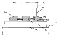
図4Aに示すように、ステージ7a(または専用のステージ)により保持された基板12に対して、各電極12aと、対応する各電極14aとが正対するように位置決めをし、その状態で、加圧用アクチュエータにより電子部品14を基板12に向かって押圧しながら、加熱手段により、電子部品14を介してはんだ22および接着剤24を加熱する。なお、ステージ7a(または専用のステージ)に加熱手段を含ませることで、はんだ22および接着剤24の加熱を補助してもよい。図4Bに、はんだ22が電極12aに押し付けられ、加熱されている状態を示す。
As shown in FIG. 4A, the
はんだ22および接着剤24の加熱が進むと、図4Cに示すように、はんだ22が溶融し、その溶融はんだ22aが電極14aおよび12aに濡れ拡がる。さらに加熱が進むと、接着剤24が硬化し、その硬化樹脂24aにより電子部品14と基板12との接合部が封止される。
As the heating of the
ここで、はんだ22の組成は特に限定されない。しかしながら、低温度でのはんだ付けを可能にして、電子部品14等に与える熱ダメージを低減するという観点からは、はんだ22には、できるだけ低融点のはんだを使用するのが好ましい。例えば、Sn(融点:232℃)およびBi(融点:271℃)の合金を含むSn−Bi系はんだ(例えば、Sn−Bi58はんだ、Sn−57Bi−1Agはんだ)を使用するのが好ましい。他に、Sn−Zn系はんだも比較的融点が低い点で好ましい。
Here, the composition of the
その後、実装ユニット5による、溶融はんだ22aを含む接合領域の徐冷が開始される。これにより、図4Dに示すように、溶融はんだ22aが固化して、はんだ接合部26が形成される。このとき、接合領域を、はんだ22の組成に応じた適宜の条件で徐冷すると、2つの領域AR1およびAR2を有するはんだ接合部26が形成される。
Thereafter, the mounting
このとき、はんだ接合部26の中央側の領域AR1には、例えばSn−Bi系はんだであれば、偏析により、元のはんだ22に比べて、融点が高い方の元素であるBiが多く含まれることになる。一方、はんだ接合部26の外側にある領域AR2には、例えばSn−Bi系はんだであれば、偏析により、元のはんだ22に比べて、融点が低い方の元素であるSnが多く含まれることになる。
At this time, the region AR1 on the center side of the solder
上記の例において、Biは脆さが大きい金属であることから、領域AR1のBiの量が多すぎると、はんだ接合部26全体の強度が低下する可能性がある。しかしながら、接合領域を徐冷する条件を適宜なものに設定することで、偏析の程度を適度に調節することが可能となり、はんだ接合部26の強度低下を抑えることができる。また、たとえ、はんだ接合部26の強度が低下しても、その低下分を、硬化樹脂の接合力により補うことができる。
In the above example, since Bi is a highly brittle metal, if the amount of Bi in the area AR1 is too large, the strength of the entire solder joint 26 may be reduced. However, it is possible to appropriately adjust the degree of segregation by setting the conditions for slowly cooling the joining region, and the strength reduction of the solder
その一方で、領域AR1およびAR2が元のはんだ22の濃度と異なる濃度のBiを含むことで、各領域が、接合領域を徐冷しないときに形成される通常のはんだ接合部に比べて高融点化される。これにより、例えば、232℃以上、かつ271℃以下の高融点を有し、かつ十分な強度を有するはんだ接合部26を形成することが可能となる。
On the other hand, since the regions AR1 and AR2 contain Bi having a concentration different from the concentration of the
以上の結果、例えば、基板12に電子部品14を実装することで作製された電子部品モジュールを他の基板等にリフロー方式で再実装しても、はんだ接合部26の信頼性が低下するのを防止することができる。
As a result of the above, for example, even when an electronic component module manufactured by mounting the
(基板の電極がはんだを含む場合)
基板12の電極12aがはんだを含む場合も基本的には電子部品14の電極14aがはんだを含む場合と同様のプロセスで、電極12aと電極14aとの間にはんだ接合部26を形成することができる。これにより、上の場合と同様に、通常のはんだ接合部よりも高融点のはんだ接合部26を形成することができる。なお、電極12aにクリームはんだを塗布することで電極12aにはんだ22を含ませる場合には、ライン1にスクリーン印刷装置等を付加することができる。
(When the electrode on the board contains solder)
Even when the
(接着剤がはんだを含む場合)
図5Aに示すように、はんだを、はんだ粒子22bとして接着剤24に含ませ、ペーストとすることで、電極12aおよび電極14aにはんだ22を供給することができる。そのようなはんだ粒子22bの融点は、上述のSn−Bi系はんだであれば例えば138℃である。上記ペーストに含まれるはんだ粒子22bの含有量は、例えば4〜30質量%とすることができる。はんだ粒子の平均粒径は、例えば2〜10μmであるが、特に限定されるものではない。
(When the adhesive contains solder)
As shown in FIG. 5A, the
そして、上述したのと同様の加圧および加熱のプロセスで電子部品14を基板12に向かって押圧することで、図5Bに示すように、電極12aと電極14aとの間にはんだ粒子22bが挟まれ、加熱される。そして、加熱によりはんだ粒子22bが溶融すると、図5Cに示すように、溶融はんだ22aが電極12aおよび電極14aに濡れ拡がる。さらに加熱が進むと、接着剤24が硬化し、その硬化樹脂24aにより電子部品14が基板12に接着される。なお、接着剤24には、はんだや電極の酸化物被膜を除去する作用を有する活性剤を含ませることができる。
Then, by pressing the
その後、溶融はんだ22aの徐冷が開始され、これにより、上述したのと同様のプロセスで、領域AR1および領域AR2を有するはんだ接合部26が形成される。これにより、十分な強度および、通常よりも高融点を有するはんだ接合部26を形成することが可能となる。
Thereafter, the slow cooling of the
このように、接着剤24にはんだ粒子22bを含ませる形態では、ライン1に、クリームはんだ等の低融点はんだを供給するための特別の機構(例えばスクリーン印刷装置)を付加する必要性がなくなる。これにより、ライン1をより安価に構築できる。また、クリームはんだ等の塗布工程が省略できることから、さらに生産効率を向上させることが容易となる。
Thus, in the form in which the
(実施形態2)
次に、図6を参照して、本発明の実施形態2を説明する。図6は、本実施形態に係る回路部材接合ラインの概略構成を示すブロック図である。
(Embodiment 2)
Next,
図示例のライン1Aは、図1のライン1と同様に、基板12に電子部品14を実装するためのラインとして構成されている。より具体的には、ライン1Aは、図1のライン1と同様の、投入ユニット2、クリーナ3、接着剤塗布ユニット4、実装機5A、回収ユニット6、およびコンベア7を含むとともに、実装機5Aと回収ユニット6との間に配置されたオーブン(またはリフロー炉)8を含んでいる。ライン1Aでは、実装機5Aとオーブン8との組み合わせが、電子部品14の基板12に対する実装工程を実行する実装ユニットとして機能する。以下、ライン1Aが図1のライン1と異なる点を主に説明する。
The
ライン1Aにおいては、実装機5Aは、図示しない冷却ファン等の冷却装置を備えている。実装機5Aにおいて、電極12aと電極14aとの間に溶融はんだ22aが形成されるまでのプロセス(図4A〜4Cまたは図5A〜5Cにより示すプロセス)は、図1のライン1におけるプロセスと同様である。ライン1Aにおいては、溶融はんだ22aを含む接合領域は徐冷されず、上記の冷却装置により急冷される。
In the line 1A, the mounting
以上の処理により、電極12aと電極14aとが、通常のはんだ接合部により接合されて、基板12に電子部品14が仮実装される。このとき、ここまでの処理には、徐冷のプロセスが含まれないために、図1の実装ユニット5における実装と比較して、短時間で基板12に全ての電子部品14が仮実装される。
Through the above processing, the
オーブン8は、電子部品14が仮実装された基板12(以下、そのような状態の基板を電子部品接合基板ともいう)を、再度、はんだ接合部が溶融するまで加熱する。これにより、電子部品接合基板は、再び、図4Cまたは図5Cに示したのと同じ状態となる。この電子部品接合基板の接合領域を、図1のライン1における条件と同じ条件で徐冷する。これにより、図1のライン1と同様に高融点かつ十分な強度を有するはんだ接合部26を形成することが可能となる。
The
そして、ライン1Aにおいては、徐冷のプロセスを基板12に実装される全ての電子部品14に対して一括して実行することができる。これにより、1つの基板12に実装される電子部品14の数が多数であるような場合には、電子部品接合基板の製造に要する時間を大幅に短縮することが可能となる。
In the
(実施形態3)
次に、図7〜図9を参照して、本発明の実施形態3を説明する。図7は、本実施形態に係る回路部材接合ラインの概略構成を示すブロック図である。図8は、プレス機のプレス台の上面図である。図9は、プレス機の動作を説明する説明図であって、プレス機の側面図である。
(Embodiment 3)
Next,
図示例のライン1Bは、図1のライン1と同様に、基板12に複数の電子部品14を実装するためのラインとして構成されている。より具体的には、ライン1Bは、図1のライン1と同様の、投入ユニット2、クリーナ3、接着剤塗布ユニット4、回収ユニット6、およびコンベア7を含む。ライン1Bにおいては、さらに、接着剤塗布ユニット4と回収ユニット6との間に、仮載せ機9およびプレス機10が配置されている。ライン1Bでは、仮載せ機9とプレス機10との組み合わせが、電子部品14の基板12に対する実装工程を実行する実装ユニットとして機能する。以下、ライン1Bが図1のライン1および図6のライン1Aと異なる点を主に説明する。
The line 1B in the illustrated example is configured as a line for mounting a plurality of
仮載せ機9は、接着剤塗布ユニット4の下流に配置されている。仮載せ機9も、図3に示した実装ユニット5と同様に、複数の電子部品14が載置される部品供給ステージ18と、図示しない3軸移動機構と、制御部9aとを備えている。仮載せ機9が実装ユニット5と異なるのは、実装ヘッド20の代わりに仮置きヘッド28を有する点である。仮置きヘッド28は、実装ヘッド20とは異なり、加熱手段を必須の構成要素として有していない。仮置きヘッド28および3軸移動機構の動作は、制御部9aにより制御される。
The
仮載せ機9の3軸移動機構が制御部9aの位置決め制御により制御され、これにより、仮置きヘッド28が、X軸方向、Y軸方向およびZ軸方向の3軸方向に移動される点、および、制御部9aの制御により、部品供給ステージ18上の電子部品14が仮置きヘッド28によりピックアップされる点は、実装ユニット5と同様である。さらに、電子部品14を保持した状態の仮置きヘッド28が、3軸移動機構により、当該電子部品14と対応する電子部品実装位置MPの上方に移動され、その電子部品実装位置MPで、各電極14aを、対応する各電極12aとそれぞれ対向させて、電子部品14を基板12に向かって押し付ける点も同様である。このとき、その電子部品実装位置MPに、既に接着剤塗布ユニット4により接着剤が塗布されている点も同様である。
The triaxial movement mechanism of the
仮載せ機9が実装ユニット5と異なるのは、仮載せ機9においては、仮置きヘッド28が、電子部品14を接着剤の上から基板12に向かって押し付けるようにして、電子部品14を基板12の上に置くだけの動作しかせず、電極同士を接合する動作をしない点である。このため、仮載せ機9における基板12の1個あたりの処理時間は、実装ユニット5のそれよりも格段に短くなっている。
The
仮載せ機9の下流に配されたプレス機10は、図8に示すように、それぞれが複数の電子部品14を仮置きされた複数の基板12を載置するためのプレス台30を有している。仮載せ機9で処理された各基板12は、プレス台30の上に順次載置されていく。
As shown in FIG. 8, the
プレス機10は、さらに、図9に示すように、各基板12の上に載置された複数の電子部品14を基板12に向かって同時に押圧するためのプレス板32を有している。プレス板32は、基板12毎に独立して設けてもよいし、複数の基板12に対して1つのプレス板32を設けてもよい。
As shown in FIG. 9, the
プレス板32およびプレス台30の少なくとも一方には、はんだ22(図9の例では、はんだ粒子22b)および接着剤24を加熱するための加熱手段を含ませることができる。それらの加熱手段により加熱しながら各電子部品14をプレス板32により基板12に向かって押圧する。これにより、図4Cまたは図5Cに示したように、はんだ22が溶融した溶融はんだ22aが、各電極14aと、対応する各電極12aとの間に濡れ拡がるとともに、各電子部品14と基板12とが硬化樹脂24aにより封止される。
At least one of the
その後、上記の各実施形態と同様の条件で各電子部品14の接合領域を一括して徐冷することで、上記の各実施形態と同様の高融点かつ十分な強度のはんだ接合部26により各電極12aに、対応する各電極14aを接合することが可能となる。なお、プレス板32の下面およびプレス台30の上面の少なくとも一方をセラミックにより形成することで、保温性を高めてもよい。
Thereafter, the joint region of each
以上により、徐冷のプロセスを複数の基板12に対して一括して実行することで、複数の基板12のそれぞれに複数の電子部品14を接合することが可能となり、生産効率を大幅に向上させることができる。
As described above, by performing the slow cooling process on the plurality of
次に、本発明の実施例を説明する。なお、本発明は、以下の実施例に限定されない。
(実施例1)
接着剤として、エポキシ樹脂、硬化剤、チキソ剤、顔料、カップリング剤を含む樹脂組成物を使用した。それに、Sn−Bi系はんだ(Sn−58Biはんだ)の微粒子(平均粒径:4.8μm、融点:138℃)を20重量%だけ混合することで、はんだ粒子含有接着剤(ペースト)を調製した。
Next, examples of the present invention will be described. In addition, this invention is not limited to a following example.
Example 1
As the adhesive, a resin composition containing an epoxy resin, a curing agent, a thixotropic agent, a pigment, and a coupling agent was used. A solder particle-containing adhesive (paste) was prepared by mixing only 20% by weight of Sn—Bi solder (Sn-58Bi solder) fine particles (average particle diameter: 4.8 μm, melting point: 138 ° C.). .
Cu電極を有する試験用基板を用意した。試験用基板の各Cu電極と対応する、それぞれが184個の電極を有する試験用電子部品を用意した。試験用基板の各Cu電極をパナソニック・ファクトリー・ソリューションズ株式会社製のプラズマ処理装置によりプラズマ処理した。その後、電子部品実装位置MPに上記のはんだ粒子含有接着剤を岩下エンジニアリング株式会社製の接着剤塗布ユニットにより適量ずつ塗布した。図1の実装ユニット5と同様の構成の、パナソニック ファクトリーソリューションズ株式会社製の実装機により、試験用電子部品を基板に搭載し、当該部品の各電極と、対応する各基板電極との間に、溶融はんだを形成した後、その溶融はんだを含む接合領域を徐冷した。実装条件は下記の通りである。
A test substrate having a Cu electrode was prepared. Test electronic components each having 184 electrodes corresponding to each Cu electrode of the test substrate were prepared. Each Cu electrode of the test substrate was subjected to plasma treatment using a plasma processing apparatus manufactured by Panasonic Factory Solutions Co., Ltd. Thereafter, an appropriate amount of the above solder particle-containing adhesive was applied to the electronic component mounting position MP by an adhesive application unit manufactured by Iwashita Engineering Co., Ltd. A mounting device manufactured by Panasonic Factory Solutions Co., Ltd. having a configuration similar to that of the mounting
実装ヘッドの温度:218℃
実装ヘッドによる荷重:電極1個あたり0.1N
加熱時間:15秒
接合領域が138〜200℃の温度領域に留まっていたと推定される時間(以下、徐冷時間という):20秒
冷却速度:3℃/秒(138〜200℃の温度範囲TRの平均冷却速度)
Mounting head temperature: 218 ° C
Load by mounting head: 0.1N per electrode
Heating time: 15 seconds Time when the bonding region is estimated to remain in the temperature region of 138 to 200 ° C. (hereinafter referred to as slow cooling time): 20 seconds Cooling rate: 3 ° C./second (temperature range TR of 138 to 200 ° C. Average cooling rate)
上記の条件により、1つの試験用基板に10個の電子部品を1つずつ実装した。 Under the above conditions, ten electronic components were mounted one by one on one test substrate.
(実施例2)
下記の条件が異なること以外は、実施例1と同様にして、10個の試験用電子部品を1つの試験用基板に実装した。
冷却速度:10℃/秒
徐冷時間:6秒
(Example 2)
Ten test electronic components were mounted on one test substrate in the same manner as in Example 1 except that the following conditions were different.
Cooling rate: 10 ° C./second Slow cooling time: 6 seconds
(実施例3)
下記の条件が異なること以外は、実施例1と同様にして、10個の試験用電子部品を1つの試験用基板に実装した。
冷却速度:1℃/秒
徐冷時間:60秒
Example 3
Ten test electronic components were mounted on one test substrate in the same manner as in Example 1 except that the following conditions were different.
Cooling rate: 1 ° C / second Annealing time: 60 seconds
(実施例4)
10個の試験用電子部品を1つの試験用基板に実施形態3と同様のプロセスで仮置きした。それを6回繰り返すことで、10個の試験用電子部品がそれぞれ仮置きされた6個の試験用基板(部品仮置き基板という)を得た。6個の部品仮置き基板の各試験用電子部品を、実施例1と同じ条件で各試験用基板に実装するように、エヌピーエーシステム株式会社製のプレス機を使用して加圧および加熱のプロセスを実行した後、接合領域を徐冷した。
Example 4
Ten test electronic components were temporarily placed on one test substrate in the same process as in the third embodiment. By repeating this six times, six test substrates (referred to as component temporary placement substrates) on which ten test electronic components were temporarily placed were obtained. In order to mount each test electronic component of the six component temporary placement substrates on each test substrate under the same conditions as in Example 1, pressurization and heating were performed using a press machine manufactured by NP System Co., Ltd. After performing the process, the bonded area was slowly cooled.
(比較例1)
下記条件に示すように、接合領域を冷却装置により急冷し、徐冷しなかったこと以外は、実施例1と同様にして、試験用電子部品を試験用基板に実装した。
(Comparative Example 1)
As shown in the following conditions, the test electronic component was mounted on the test substrate in the same manner as in Example 1 except that the bonding region was rapidly cooled by a cooling device and not slowly cooled.
冷却速度:25℃/秒
接合領域が138〜200℃の温度領域に留まっていたと推定される時間:2.5秒
Cooling rate: 25 ° C./second Estimated time that the bonding region remained in the temperature region of 138 to 200 ° C .: 2.5 seconds
実施例1〜4、比較例1で作製した電子部品実装基板を260℃で再加熱して、基板の配線抵抗を含む電子部品の接続抵抗値を測定した。初期の接続抵抗値から20%上昇する温度を確認したところ、実施例1〜4の各温度は、それぞれ、197℃、183℃、211℃、195℃であった。これに対して、比較例1の温度は、146℃であった。一方、実施例1〜4のはんだ接合部の1個あたりの強度は、それぞれ、0.51、0.50、0.54、0.50Nであった。これに対して、比較例1のはんだ接合部の1個あたりの強度は、0.49Nであった。 The electronic component mounting substrates produced in Examples 1 to 4 and Comparative Example 1 were reheated at 260 ° C., and the connection resistance values of the electronic components including the wiring resistance of the substrate were measured. When the temperature which rose 20% from the initial connection resistance value was confirmed, each temperature of Examples 1-4 was 197 degreeC, 183 degreeC, 211 degreeC, and 195 degreeC, respectively. On the other hand, the temperature of Comparative Example 1 was 146 ° C. On the other hand, the intensity | strength per piece of the solder joint part of Examples 1-4 was 0.51, 0.50, 0.54, and 0.50N, respectively. On the other hand, the strength per solder joint of Comparative Example 1 was 0.49N.
以上の結果によれば、実施例1〜4は、いずれも比較例1よりもはんだ接合部が高融点化していることが分かる。そして、実施例1〜4のはんだ接合部の1個あたりの強度はいずれも望ましい強度(0.10N)を上回っていることが分かる。なお、実施例1〜4の方が、比較例1よりも、若干ではあるが、はんだ接合部の強度がむしろ高くなっている。これは、実施例1〜4では接合領域が徐冷されたために、結果として熱硬化性樹脂の加熱時間が長くなり、これにより、比較例1よりも、樹脂の硬化反応が進んだものと考えられる。その結果、はんだ接合部による接合をより有効に補強し得たものと考えられる。 From the above results, it can be seen that in Examples 1 to 4, the solder joints have higher melting points than Comparative Example 1. And it turns out that the intensity | strength per one of the solder joint part of Examples 1-4 is over the desirable intensity | strength (0.10N). In Examples 1 to 4, the strength of the solder joint is rather higher than that of Comparative Example 1, although it is slightly higher. This is because the bonding region was gradually cooled in Examples 1 to 4, and as a result, the heating time of the thermosetting resin became longer, and as a result, the resin curing reaction proceeded more than in Comparative Example 1. It is done. As a result, it is considered that the joining by the solder joint portion could be reinforced more effectively.
さらに、実施例4においては、6つの試験用基板の全てに試験用電子部品を実装するのに要した時間が78秒であった。これに対して、実施例1では、6つの試験用基板の全てに試験用電子部品を実装するのに要した時間が393秒であった。この結果から、実施例4によれば、生産効率を格段に向上させ得ることが理解される。 Furthermore, in Example 4, the time required to mount the test electronic components on all six test substrates was 78 seconds. In contrast, in Example 1, the time required to mount the test electronic components on all six test substrates was 393 seconds. From this result, it is understood that according to Example 4, the production efficiency can be remarkably improved.
本発明によれば、比較的低温でのはんだ付けにより、高融点かつ十分な強度を有するはんだ接合部を形成できるので、本発明は、様々な回路部材接合構造体、特に、再リフローが予定される電子部品モジュールを含む構造体において有用である。 According to the present invention, a solder joint having a high melting point and sufficient strength can be formed by soldering at a relatively low temperature. Therefore, the present invention is intended for various circuit member joint structures, in particular, re-reflow. This is useful in a structure including an electronic component module.
1、1A、1B…ライン、
3…クリーナ、
4…接着剤塗布ユニット、
5…実装ユニット、
5A…実装機、
7…コンベア、
7a…ステージ、
8…オーブン、
9…仮載せ機、
10…プレス機、
12…基板、
12a…電極、
14…電子部品、
14a…電極、
16…塗布ヘッド、
18…部品供給ステージ、
22a…溶融はんだ、
20…実装ヘッド、
22b…はんだ粒子、
24…接着剤、
24a…硬化樹脂、
26…はんだ接合部、
28…仮置きヘッド、
30…プレス台、
32…プレス板、
1, 1A, 1B ... line,
3 ... Cleaner,
4 ... Adhesive application unit,
5 ... Mounting unit,
5A ... Mounting machine,
7 ... conveyor,
7a ... stage,
8 ... Oven,
9 ... Temporary loading machine,
10 ... Press machine,
12 ... substrate
12a ... electrodes,
14 ... electronic components,
14a ... electrodes,
16 ... coating head,
18 ... parts supply stage,
22a ... Molten solder,
20: Mounting head,
22b ... solder particles,
24. Adhesive,
24a ... cured resin,
26: Solder joint,
28 ... Temporary placement head,
30 ... Press stand,
32 ... press plate,
Claims (12)
前記第一接続用電極と対向する第二接続用電極を有する第二回路部材と、
前記第一接続用電極と、前記第二接続用電極との間に介在し、前記第一接続用電極と、前記第二接続用電極とを電気的に接続するはんだ接合部と、を具備し、
前記はんだ接合部が、金属部分を含み、
前記金属部分は、第一金属元素を主成分として含む第一金属領域と、前記第一金属元素よりも融点の高い第二金属元素を主成分として含む第二金属領域と、を含み、
前記第一金属領域は、前記はんだ接合部の外側で前記第一接続用電極と前記第二接続用電極とを接合し、
前記第二金属領域は、前記はんだ接合部の中央側で前記第一接続用電極と前記第二接続用電極とを接合し、
前記第一金属元素は前記第二金属元素と合金を形成可能であり、かつ前記合金の融点は、前記第一金属領域の融点および前記第二金属領域の融点よりも低く、
前記第一金属領域および前記第二金属領域は、いずれも前記合金の構成元素の偏析により生成した領域である、回路部材接合構造体。 A first circuit member having a first connection electrode;
A second circuit member having a second connection electrode facing the first connection electrode;
A solder joint interposed between the first connection electrode and the second connection electrode and electrically connecting the first connection electrode and the second connection electrode; ,
The solder joint includes a metal portion;
The metal portion includes a first metal region containing a first metal element as a main component, and a second metal region containing a second metal element having a melting point higher than that of the first metal element as a main component,
The first metal region joins the first connection electrode and the second connection electrode outside the solder joint,
The second metal region joins the first connection electrode and the second connection electrode on the center side of the solder joint,
The first metal element may be formed of the second metal elements and alloys, and the melting point of the alloy, rather lower than the melting point of the melting point and the second metal region of the first metal region,
Both said 1st metal area | region and said 2nd metal area | region are the area | regions produced | generated by segregation of the constituent element of the said alloy .
Priority Applications (1)
| Application Number | Priority Date | Filing Date | Title |
|---|---|---|---|
| JP2012059175A JP6037300B2 (en) | 2012-03-15 | 2012-03-15 | Circuit member joint structure |
Applications Claiming Priority (1)
| Application Number | Priority Date | Filing Date | Title |
|---|---|---|---|
| JP2012059175A JP6037300B2 (en) | 2012-03-15 | 2012-03-15 | Circuit member joint structure |
Publications (2)
| Publication Number | Publication Date |
|---|---|
| JP2013197111A JP2013197111A (en) | 2013-09-30 |
| JP6037300B2 true JP6037300B2 (en) | 2016-12-07 |
Family
ID=49395760
Family Applications (1)
| Application Number | Title | Priority Date | Filing Date |
|---|---|---|---|
| JP2012059175A Active JP6037300B2 (en) | 2012-03-15 | 2012-03-15 | Circuit member joint structure |
Country Status (1)
| Country | Link |
|---|---|
| JP (1) | JP6037300B2 (en) |
Families Citing this family (2)
| Publication number | Priority date | Publication date | Assignee | Title |
|---|---|---|---|---|
| JP2017037931A (en) * | 2015-08-07 | 2017-02-16 | 東レエンジニアリング株式会社 | Solder joint method of mounting component and solder joint device of mounting component |
| JP6508344B2 (en) * | 2015-08-28 | 2019-05-08 | 日立化成株式会社 | Composition for buffer sheet and buffer sheet |
Family Cites Families (5)
| Publication number | Priority date | Publication date | Assignee | Title |
|---|---|---|---|---|
| JP3348528B2 (en) * | 1994-07-20 | 2002-11-20 | 富士通株式会社 | Method for manufacturing semiconductor device, method for manufacturing semiconductor device and electronic circuit device, and electronic circuit device |
| JP4097813B2 (en) * | 1998-10-28 | 2008-06-11 | 内橋エステック株式会社 | Soldering method |
| JP2011077308A (en) * | 2009-09-30 | 2011-04-14 | Fujitsu Ltd | Method for mounting semiconductor device |
| JP6028449B2 (en) * | 2011-10-05 | 2016-11-16 | 富士通株式会社 | Semiconductor device, electronic device, and manufacturing method of semiconductor device |
| JP5853135B2 (en) * | 2012-03-15 | 2016-02-09 | パナソニックIpマネジメント株式会社 | Electrode joining method and circuit member joining line |
-
2012
- 2012-03-15 JP JP2012059175A patent/JP6037300B2/en active Active
Also Published As
| Publication number | Publication date |
|---|---|
| JP2013197111A (en) | 2013-09-30 |
Similar Documents
| Publication | Publication Date | Title |
|---|---|---|
| US6235996B1 (en) | Interconnection structure and process module assembly and rework | |
| JP6011887B2 (en) | Electronic component mounting method and electronic component mounting line | |
| JP6057224B2 (en) | Component mounting structure | |
| JP5519866B2 (en) | Electronic component mounting line and electronic component mounting method | |
| JP5719999B2 (en) | Electronic component mounting method, electronic component mounting apparatus, and electronic component mounting system | |
| JP5093766B2 (en) | Manufacturing method of semiconductor package substrate mounted with conductive balls, etc. | |
| JP2008109009A (en) | Method of manufacturing semiconductor device | |
| US9125329B2 (en) | Electronic component mounting line and electronic component mounting method | |
| US9439335B2 (en) | Electronic component mounting line and electronic component mounting method | |
| JP5853135B2 (en) | Electrode joining method and circuit member joining line | |
| JP6037300B2 (en) | Circuit member joint structure | |
| TWI453845B (en) | Method for manufacturing semiconductor device | |
| JP2018181939A (en) | Mounting structure of semiconductor component | |
| JP6135892B2 (en) | Electronic component mounting method and electronic component mounting line | |
| JP2006332354A (en) | Printed circuit board and manufacturing method thereof | |
| JP2014033084A (en) | Manufacturing method of lamination package structure, assembling device and manufacturing system | |
| JP6135891B2 (en) | Electronic component mounting method and electronic component mounting line | |
| JP5719997B2 (en) | Electronic component mounting method and mounting system | |
| JP2001185577A (en) | Electronic appliances | |
| JP5887547B2 (en) | Flux for solder joint and manufacturing method thereof | |
| JP5828095B2 (en) | Electronic component mounting structure manufacturing method and electronic component mounting apparatus | |
| KR101214683B1 (en) | Method for manufacturing semiconductor device | |
| JP2014049646A (en) | Part mounting method and part mounting system | |
| JP2022105279A (en) | Method and device (assembly of chip and substrate) | |
| JP5884088B2 (en) | Electronic component mounting method |
Legal Events
| Date | Code | Title | Description |
|---|---|---|---|
| A621 | Written request for application examination |
Free format text: JAPANESE INTERMEDIATE CODE: A621 Effective date: 20140710 |
|
| A711 | Notification of change in applicant |
Free format text: JAPANESE INTERMEDIATE CODE: A711 Effective date: 20141009 |
|
| RD03 | Notification of appointment of power of attorney |
Free format text: JAPANESE INTERMEDIATE CODE: A7423 Effective date: 20141028 |
|
| A977 | Report on retrieval |
Free format text: JAPANESE INTERMEDIATE CODE: A971007 Effective date: 20150624 |
|
| A131 | Notification of reasons for refusal |
Free format text: JAPANESE INTERMEDIATE CODE: A131 Effective date: 20150630 |
|
| A521 | Written amendment |
Free format text: JAPANESE INTERMEDIATE CODE: A523 Effective date: 20150824 |
|
| A131 | Notification of reasons for refusal |
Free format text: JAPANESE INTERMEDIATE CODE: A131 Effective date: 20160315 |
|
| A521 | Written amendment |
Free format text: JAPANESE INTERMEDIATE CODE: A523 Effective date: 20160421 |
|
| TRDD | Decision of grant or rejection written | ||
| A01 | Written decision to grant a patent or to grant a registration (utility model) |
Free format text: JAPANESE INTERMEDIATE CODE: A01 Effective date: 20161004 |
|
| A61 | First payment of annual fees (during grant procedure) |
Free format text: JAPANESE INTERMEDIATE CODE: A61 Effective date: 20161024 |
|
| R151 | Written notification of patent or utility model registration |
Ref document number: 6037300 Country of ref document: JP Free format text: JAPANESE INTERMEDIATE CODE: R151 |