JP6035132B2 - Liquid crystal display - Google Patents
Liquid crystal display Download PDFInfo
- Publication number
- JP6035132B2 JP6035132B2 JP2012267279A JP2012267279A JP6035132B2 JP 6035132 B2 JP6035132 B2 JP 6035132B2 JP 2012267279 A JP2012267279 A JP 2012267279A JP 2012267279 A JP2012267279 A JP 2012267279A JP 6035132 B2 JP6035132 B2 JP 6035132B2
- Authority
- JP
- Japan
- Prior art keywords
- calibration
- electrode
- detection
- voltage
- liquid crystal
- Prior art date
- Legal status (The legal status is an assumption and is not a legal conclusion. Google has not performed a legal analysis and makes no representation as to the accuracy of the status listed.)
- Active
Links
- 239000004973 liquid crystal related substance Substances 0.000 title claims description 82
- 238000001514 detection method Methods 0.000 claims description 181
- 239000000758 substrate Substances 0.000 claims description 48
- 239000003990 capacitor Substances 0.000 claims description 37
- 230000010354 integration Effects 0.000 claims description 36
- 238000000034 method Methods 0.000 claims description 14
- 230000008569 process Effects 0.000 claims description 12
- 239000011159 matrix material Substances 0.000 claims 5
- 230000007547 defect Effects 0.000 description 12
- 238000007689 inspection Methods 0.000 description 12
- 238000010586 diagram Methods 0.000 description 10
- 230000008859 change Effects 0.000 description 4
- 239000002184 metal Substances 0.000 description 3
- 230000035945 sensitivity Effects 0.000 description 3
- 239000004840 adhesive resin Substances 0.000 description 2
- 229920006223 adhesive resin Polymers 0.000 description 2
- 238000006243 chemical reaction Methods 0.000 description 2
- 239000004020 conductor Substances 0.000 description 2
- 230000007423 decrease Effects 0.000 description 2
- 238000005516 engineering process Methods 0.000 description 2
- 239000011521 glass Substances 0.000 description 2
- 239000000203 mixture Substances 0.000 description 2
- -1 polarizing plates Substances 0.000 description 2
- 101000633613 Homo sapiens Probable threonine protease PRSS50 Proteins 0.000 description 1
- 102100029523 Probable threonine protease PRSS50 Human genes 0.000 description 1
- 230000009471 action Effects 0.000 description 1
- 238000013459 approach Methods 0.000 description 1
- 230000003247 decreasing effect Effects 0.000 description 1
- 230000002950 deficient Effects 0.000 description 1
- 230000000694 effects Effects 0.000 description 1
- 230000005611 electricity Effects 0.000 description 1
- 238000000605 extraction Methods 0.000 description 1
- 238000004519 manufacturing process Methods 0.000 description 1
- 238000012986 modification Methods 0.000 description 1
- 230000004048 modification Effects 0.000 description 1
- 230000003071 parasitic effect Effects 0.000 description 1
- 229920001690 polydopamine Polymers 0.000 description 1
- 238000003825 pressing Methods 0.000 description 1
- 230000001681 protective effect Effects 0.000 description 1
- 230000009467 reduction Effects 0.000 description 1
- 229920006395 saturated elastomer Polymers 0.000 description 1
- 230000003068 static effect Effects 0.000 description 1
Images


Classifications
-
- G—PHYSICS
- G02—OPTICS
- G02F—OPTICAL DEVICES OR ARRANGEMENTS FOR THE CONTROL OF LIGHT BY MODIFICATION OF THE OPTICAL PROPERTIES OF THE MEDIA OF THE ELEMENTS INVOLVED THEREIN; NON-LINEAR OPTICS; FREQUENCY-CHANGING OF LIGHT; OPTICAL LOGIC ELEMENTS; OPTICAL ANALOGUE/DIGITAL CONVERTERS
- G02F1/00—Devices or arrangements for the control of the intensity, colour, phase, polarisation or direction of light arriving from an independent light source, e.g. switching, gating or modulating; Non-linear optics
- G02F1/01—Devices or arrangements for the control of the intensity, colour, phase, polarisation or direction of light arriving from an independent light source, e.g. switching, gating or modulating; Non-linear optics for the control of the intensity, phase, polarisation or colour
- G02F1/13—Devices or arrangements for the control of the intensity, colour, phase, polarisation or direction of light arriving from an independent light source, e.g. switching, gating or modulating; Non-linear optics for the control of the intensity, phase, polarisation or colour based on liquid crystals, e.g. single liquid crystal display cells
- G02F1/133—Constructional arrangements; Operation of liquid crystal cells; Circuit arrangements
- G02F1/1333—Constructional arrangements; Manufacturing methods
- G02F1/13338—Input devices, e.g. touch panels
-
- G—PHYSICS
- G09—EDUCATION; CRYPTOGRAPHY; DISPLAY; ADVERTISING; SEALS
- G09G—ARRANGEMENTS OR CIRCUITS FOR CONTROL OF INDICATING DEVICES USING STATIC MEANS TO PRESENT VARIABLE INFORMATION
- G09G3/00—Control arrangements or circuits, of interest only in connection with visual indicators other than cathode-ray tubes
- G09G3/20—Control arrangements or circuits, of interest only in connection with visual indicators other than cathode-ray tubes for presentation of an assembly of a number of characters, e.g. a page, by composing the assembly by combination of individual elements arranged in a matrix no fixed position being assigned to or needed to be assigned to the individual characters or partial characters
- G09G3/34—Control arrangements or circuits, of interest only in connection with visual indicators other than cathode-ray tubes for presentation of an assembly of a number of characters, e.g. a page, by composing the assembly by combination of individual elements arranged in a matrix no fixed position being assigned to or needed to be assigned to the individual characters or partial characters by control of light from an independent source
- G09G3/36—Control arrangements or circuits, of interest only in connection with visual indicators other than cathode-ray tubes for presentation of an assembly of a number of characters, e.g. a page, by composing the assembly by combination of individual elements arranged in a matrix no fixed position being assigned to or needed to be assigned to the individual characters or partial characters by control of light from an independent source using liquid crystals
-
- G—PHYSICS
- G02—OPTICS
- G02F—OPTICAL DEVICES OR ARRANGEMENTS FOR THE CONTROL OF LIGHT BY MODIFICATION OF THE OPTICAL PROPERTIES OF THE MEDIA OF THE ELEMENTS INVOLVED THEREIN; NON-LINEAR OPTICS; FREQUENCY-CHANGING OF LIGHT; OPTICAL LOGIC ELEMENTS; OPTICAL ANALOGUE/DIGITAL CONVERTERS
- G02F1/00—Devices or arrangements for the control of the intensity, colour, phase, polarisation or direction of light arriving from an independent light source, e.g. switching, gating or modulating; Non-linear optics
- G02F1/01—Devices or arrangements for the control of the intensity, colour, phase, polarisation or direction of light arriving from an independent light source, e.g. switching, gating or modulating; Non-linear optics for the control of the intensity, phase, polarisation or colour
- G02F1/13—Devices or arrangements for the control of the intensity, colour, phase, polarisation or direction of light arriving from an independent light source, e.g. switching, gating or modulating; Non-linear optics for the control of the intensity, phase, polarisation or colour based on liquid crystals, e.g. single liquid crystal display cells
- G02F1/1306—Details
- G02F1/1309—Repairing; Testing
-
- G—PHYSICS
- G02—OPTICS
- G02F—OPTICAL DEVICES OR ARRANGEMENTS FOR THE CONTROL OF LIGHT BY MODIFICATION OF THE OPTICAL PROPERTIES OF THE MEDIA OF THE ELEMENTS INVOLVED THEREIN; NON-LINEAR OPTICS; FREQUENCY-CHANGING OF LIGHT; OPTICAL LOGIC ELEMENTS; OPTICAL ANALOGUE/DIGITAL CONVERTERS
- G02F1/00—Devices or arrangements for the control of the intensity, colour, phase, polarisation or direction of light arriving from an independent light source, e.g. switching, gating or modulating; Non-linear optics
- G02F1/01—Devices or arrangements for the control of the intensity, colour, phase, polarisation or direction of light arriving from an independent light source, e.g. switching, gating or modulating; Non-linear optics for the control of the intensity, phase, polarisation or colour
- G02F1/13—Devices or arrangements for the control of the intensity, colour, phase, polarisation or direction of light arriving from an independent light source, e.g. switching, gating or modulating; Non-linear optics for the control of the intensity, phase, polarisation or colour based on liquid crystals, e.g. single liquid crystal display cells
- G02F1/133—Constructional arrangements; Operation of liquid crystal cells; Circuit arrangements
- G02F1/1333—Constructional arrangements; Manufacturing methods
- G02F1/1335—Structural association of cells with optical devices, e.g. polarisers or reflectors
- G02F1/133528—Polarisers
-
- G—PHYSICS
- G02—OPTICS
- G02F—OPTICAL DEVICES OR ARRANGEMENTS FOR THE CONTROL OF LIGHT BY MODIFICATION OF THE OPTICAL PROPERTIES OF THE MEDIA OF THE ELEMENTS INVOLVED THEREIN; NON-LINEAR OPTICS; FREQUENCY-CHANGING OF LIGHT; OPTICAL LOGIC ELEMENTS; OPTICAL ANALOGUE/DIGITAL CONVERTERS
- G02F1/00—Devices or arrangements for the control of the intensity, colour, phase, polarisation or direction of light arriving from an independent light source, e.g. switching, gating or modulating; Non-linear optics
- G02F1/01—Devices or arrangements for the control of the intensity, colour, phase, polarisation or direction of light arriving from an independent light source, e.g. switching, gating or modulating; Non-linear optics for the control of the intensity, phase, polarisation or colour
- G02F1/13—Devices or arrangements for the control of the intensity, colour, phase, polarisation or direction of light arriving from an independent light source, e.g. switching, gating or modulating; Non-linear optics for the control of the intensity, phase, polarisation or colour based on liquid crystals, e.g. single liquid crystal display cells
- G02F1/133—Constructional arrangements; Operation of liquid crystal cells; Circuit arrangements
- G02F1/1333—Constructional arrangements; Manufacturing methods
- G02F1/1343—Electrodes
- G02F1/134309—Electrodes characterised by their geometrical arrangement
-
- G—PHYSICS
- G02—OPTICS
- G02F—OPTICAL DEVICES OR ARRANGEMENTS FOR THE CONTROL OF LIGHT BY MODIFICATION OF THE OPTICAL PROPERTIES OF THE MEDIA OF THE ELEMENTS INVOLVED THEREIN; NON-LINEAR OPTICS; FREQUENCY-CHANGING OF LIGHT; OPTICAL LOGIC ELEMENTS; OPTICAL ANALOGUE/DIGITAL CONVERTERS
- G02F1/00—Devices or arrangements for the control of the intensity, colour, phase, polarisation or direction of light arriving from an independent light source, e.g. switching, gating or modulating; Non-linear optics
- G02F1/01—Devices or arrangements for the control of the intensity, colour, phase, polarisation or direction of light arriving from an independent light source, e.g. switching, gating or modulating; Non-linear optics for the control of the intensity, phase, polarisation or colour
- G02F1/13—Devices or arrangements for the control of the intensity, colour, phase, polarisation or direction of light arriving from an independent light source, e.g. switching, gating or modulating; Non-linear optics for the control of the intensity, phase, polarisation or colour based on liquid crystals, e.g. single liquid crystal display cells
- G02F1/133—Constructional arrangements; Operation of liquid crystal cells; Circuit arrangements
- G02F1/136—Liquid crystal cells structurally associated with a semi-conducting layer or substrate, e.g. cells forming part of an integrated circuit
- G02F1/1362—Active matrix addressed cells
- G02F1/136286—Wiring, e.g. gate line, drain line
-
- G—PHYSICS
- G02—OPTICS
- G02F—OPTICAL DEVICES OR ARRANGEMENTS FOR THE CONTROL OF LIGHT BY MODIFICATION OF THE OPTICAL PROPERTIES OF THE MEDIA OF THE ELEMENTS INVOLVED THEREIN; NON-LINEAR OPTICS; FREQUENCY-CHANGING OF LIGHT; OPTICAL LOGIC ELEMENTS; OPTICAL ANALOGUE/DIGITAL CONVERTERS
- G02F1/00—Devices or arrangements for the control of the intensity, colour, phase, polarisation or direction of light arriving from an independent light source, e.g. switching, gating or modulating; Non-linear optics
- G02F1/01—Devices or arrangements for the control of the intensity, colour, phase, polarisation or direction of light arriving from an independent light source, e.g. switching, gating or modulating; Non-linear optics for the control of the intensity, phase, polarisation or colour
- G02F1/13—Devices or arrangements for the control of the intensity, colour, phase, polarisation or direction of light arriving from an independent light source, e.g. switching, gating or modulating; Non-linear optics for the control of the intensity, phase, polarisation or colour based on liquid crystals, e.g. single liquid crystal display cells
- G02F1/133—Constructional arrangements; Operation of liquid crystal cells; Circuit arrangements
- G02F1/136—Liquid crystal cells structurally associated with a semi-conducting layer or substrate, e.g. cells forming part of an integrated circuit
- G02F1/1362—Active matrix addressed cells
- G02F1/1368—Active matrix addressed cells in which the switching element is a three-electrode device
-
- G—PHYSICS
- G06—COMPUTING; CALCULATING OR COUNTING
- G06F—ELECTRIC DIGITAL DATA PROCESSING
- G06F3/00—Input arrangements for transferring data to be processed into a form capable of being handled by the computer; Output arrangements for transferring data from processing unit to output unit, e.g. interface arrangements
- G06F3/01—Input arrangements or combined input and output arrangements for interaction between user and computer
- G06F3/03—Arrangements for converting the position or the displacement of a member into a coded form
- G06F3/041—Digitisers, e.g. for touch screens or touch pads, characterised by the transducing means
- G06F3/0412—Digitisers structurally integrated in a display
-
- G—PHYSICS
- G06—COMPUTING; CALCULATING OR COUNTING
- G06F—ELECTRIC DIGITAL DATA PROCESSING
- G06F3/00—Input arrangements for transferring data to be processed into a form capable of being handled by the computer; Output arrangements for transferring data from processing unit to output unit, e.g. interface arrangements
- G06F3/01—Input arrangements or combined input and output arrangements for interaction between user and computer
- G06F3/03—Arrangements for converting the position or the displacement of a member into a coded form
- G06F3/041—Digitisers, e.g. for touch screens or touch pads, characterised by the transducing means
- G06F3/0414—Digitisers, e.g. for touch screens or touch pads, characterised by the transducing means using force sensing means to determine a position
-
- G—PHYSICS
- G06—COMPUTING; CALCULATING OR COUNTING
- G06F—ELECTRIC DIGITAL DATA PROCESSING
- G06F3/00—Input arrangements for transferring data to be processed into a form capable of being handled by the computer; Output arrangements for transferring data from processing unit to output unit, e.g. interface arrangements
- G06F3/01—Input arrangements or combined input and output arrangements for interaction between user and computer
- G06F3/03—Arrangements for converting the position or the displacement of a member into a coded form
- G06F3/041—Digitisers, e.g. for touch screens or touch pads, characterised by the transducing means
- G06F3/0416—Control or interface arrangements specially adapted for digitisers
- G06F3/0418—Control or interface arrangements specially adapted for digitisers for error correction or compensation, e.g. based on parallax, calibration or alignment
- G06F3/04184—Synchronisation with the driving of the display or the backlighting unit to avoid interferences generated internally
-
- G—PHYSICS
- G06—COMPUTING; CALCULATING OR COUNTING
- G06F—ELECTRIC DIGITAL DATA PROCESSING
- G06F3/00—Input arrangements for transferring data to be processed into a form capable of being handled by the computer; Output arrangements for transferring data from processing unit to output unit, e.g. interface arrangements
- G06F3/01—Input arrangements or combined input and output arrangements for interaction between user and computer
- G06F3/03—Arrangements for converting the position or the displacement of a member into a coded form
- G06F3/041—Digitisers, e.g. for touch screens or touch pads, characterised by the transducing means
- G06F3/044—Digitisers, e.g. for touch screens or touch pads, characterised by the transducing means by capacitive means
- G06F3/0443—Digitisers, e.g. for touch screens or touch pads, characterised by the transducing means by capacitive means using a single layer of sensing electrodes
-
- G—PHYSICS
- G06—COMPUTING; CALCULATING OR COUNTING
- G06F—ELECTRIC DIGITAL DATA PROCESSING
- G06F3/00—Input arrangements for transferring data to be processed into a form capable of being handled by the computer; Output arrangements for transferring data from processing unit to output unit, e.g. interface arrangements
- G06F3/01—Input arrangements or combined input and output arrangements for interaction between user and computer
- G06F3/03—Arrangements for converting the position or the displacement of a member into a coded form
- G06F3/041—Digitisers, e.g. for touch screens or touch pads, characterised by the transducing means
- G06F3/044—Digitisers, e.g. for touch screens or touch pads, characterised by the transducing means by capacitive means
- G06F3/0446—Digitisers, e.g. for touch screens or touch pads, characterised by the transducing means by capacitive means using a grid-like structure of electrodes in at least two directions, e.g. using row and column electrodes
-
- G—PHYSICS
- G09—EDUCATION; CRYPTOGRAPHY; DISPLAY; ADVERTISING; SEALS
- G09G—ARRANGEMENTS OR CIRCUITS FOR CONTROL OF INDICATING DEVICES USING STATIC MEANS TO PRESENT VARIABLE INFORMATION
- G09G3/00—Control arrangements or circuits, of interest only in connection with visual indicators other than cathode-ray tubes
- G09G3/20—Control arrangements or circuits, of interest only in connection with visual indicators other than cathode-ray tubes for presentation of an assembly of a number of characters, e.g. a page, by composing the assembly by combination of individual elements arranged in a matrix no fixed position being assigned to or needed to be assigned to the individual characters or partial characters
- G09G3/34—Control arrangements or circuits, of interest only in connection with visual indicators other than cathode-ray tubes for presentation of an assembly of a number of characters, e.g. a page, by composing the assembly by combination of individual elements arranged in a matrix no fixed position being assigned to or needed to be assigned to the individual characters or partial characters by control of light from an independent source
- G09G3/36—Control arrangements or circuits, of interest only in connection with visual indicators other than cathode-ray tubes for presentation of an assembly of a number of characters, e.g. a page, by composing the assembly by combination of individual elements arranged in a matrix no fixed position being assigned to or needed to be assigned to the individual characters or partial characters by control of light from an independent source using liquid crystals
- G09G3/3611—Control of matrices with row and column drivers
- G09G3/3648—Control of matrices with row and column drivers using an active matrix
- G09G3/3655—Details of drivers for counter electrodes, e.g. common electrodes for pixel capacitors or supplementary storage capacitors
-
- G—PHYSICS
- G02—OPTICS
- G02F—OPTICAL DEVICES OR ARRANGEMENTS FOR THE CONTROL OF LIGHT BY MODIFICATION OF THE OPTICAL PROPERTIES OF THE MEDIA OF THE ELEMENTS INVOLVED THEREIN; NON-LINEAR OPTICS; FREQUENCY-CHANGING OF LIGHT; OPTICAL LOGIC ELEMENTS; OPTICAL ANALOGUE/DIGITAL CONVERTERS
- G02F1/00—Devices or arrangements for the control of the intensity, colour, phase, polarisation or direction of light arriving from an independent light source, e.g. switching, gating or modulating; Non-linear optics
- G02F1/01—Devices or arrangements for the control of the intensity, colour, phase, polarisation or direction of light arriving from an independent light source, e.g. switching, gating or modulating; Non-linear optics for the control of the intensity, phase, polarisation or colour
- G02F1/13—Devices or arrangements for the control of the intensity, colour, phase, polarisation or direction of light arriving from an independent light source, e.g. switching, gating or modulating; Non-linear optics for the control of the intensity, phase, polarisation or colour based on liquid crystals, e.g. single liquid crystal display cells
- G02F1/133—Constructional arrangements; Operation of liquid crystal cells; Circuit arrangements
- G02F1/1333—Constructional arrangements; Manufacturing methods
- G02F1/133302—Rigid substrates, e.g. inorganic substrates
-
- G—PHYSICS
- G02—OPTICS
- G02F—OPTICAL DEVICES OR ARRANGEMENTS FOR THE CONTROL OF LIGHT BY MODIFICATION OF THE OPTICAL PROPERTIES OF THE MEDIA OF THE ELEMENTS INVOLVED THEREIN; NON-LINEAR OPTICS; FREQUENCY-CHANGING OF LIGHT; OPTICAL LOGIC ELEMENTS; OPTICAL ANALOGUE/DIGITAL CONVERTERS
- G02F1/00—Devices or arrangements for the control of the intensity, colour, phase, polarisation or direction of light arriving from an independent light source, e.g. switching, gating or modulating; Non-linear optics
- G02F1/01—Devices or arrangements for the control of the intensity, colour, phase, polarisation or direction of light arriving from an independent light source, e.g. switching, gating or modulating; Non-linear optics for the control of the intensity, phase, polarisation or colour
- G02F1/13—Devices or arrangements for the control of the intensity, colour, phase, polarisation or direction of light arriving from an independent light source, e.g. switching, gating or modulating; Non-linear optics for the control of the intensity, phase, polarisation or colour based on liquid crystals, e.g. single liquid crystal display cells
- G02F1/133—Constructional arrangements; Operation of liquid crystal cells; Circuit arrangements
- G02F1/1333—Constructional arrangements; Manufacturing methods
- G02F1/1343—Electrodes
- G02F1/134309—Electrodes characterised by their geometrical arrangement
- G02F1/134318—Electrodes characterised by their geometrical arrangement having a patterned common electrode
-
- G—PHYSICS
- G02—OPTICS
- G02F—OPTICAL DEVICES OR ARRANGEMENTS FOR THE CONTROL OF LIGHT BY MODIFICATION OF THE OPTICAL PROPERTIES OF THE MEDIA OF THE ELEMENTS INVOLVED THEREIN; NON-LINEAR OPTICS; FREQUENCY-CHANGING OF LIGHT; OPTICAL LOGIC ELEMENTS; OPTICAL ANALOGUE/DIGITAL CONVERTERS
- G02F1/00—Devices or arrangements for the control of the intensity, colour, phase, polarisation or direction of light arriving from an independent light source, e.g. switching, gating or modulating; Non-linear optics
- G02F1/01—Devices or arrangements for the control of the intensity, colour, phase, polarisation or direction of light arriving from an independent light source, e.g. switching, gating or modulating; Non-linear optics for the control of the intensity, phase, polarisation or colour
- G02F1/13—Devices or arrangements for the control of the intensity, colour, phase, polarisation or direction of light arriving from an independent light source, e.g. switching, gating or modulating; Non-linear optics for the control of the intensity, phase, polarisation or colour based on liquid crystals, e.g. single liquid crystal display cells
- G02F1/133—Constructional arrangements; Operation of liquid crystal cells; Circuit arrangements
- G02F1/136—Liquid crystal cells structurally associated with a semi-conducting layer or substrate, e.g. cells forming part of an integrated circuit
- G02F1/1362—Active matrix addressed cells
- G02F1/136254—Checking; Testing
-
- G—PHYSICS
- G02—OPTICS
- G02F—OPTICAL DEVICES OR ARRANGEMENTS FOR THE CONTROL OF LIGHT BY MODIFICATION OF THE OPTICAL PROPERTIES OF THE MEDIA OF THE ELEMENTS INVOLVED THEREIN; NON-LINEAR OPTICS; FREQUENCY-CHANGING OF LIGHT; OPTICAL LOGIC ELEMENTS; OPTICAL ANALOGUE/DIGITAL CONVERTERS
- G02F2202/00—Materials and properties
- G02F2202/28—Adhesive materials or arrangements
-
- G—PHYSICS
- G06—COMPUTING; CALCULATING OR COUNTING
- G06F—ELECTRIC DIGITAL DATA PROCESSING
- G06F2203/00—Indexing scheme relating to G06F3/00 - G06F3/048
- G06F2203/041—Indexing scheme relating to G06F3/041 - G06F3/045
- G06F2203/04102—Flexible digitiser, i.e. constructional details for allowing the whole digitising part of a device to be flexed or rolled like a sheet of paper
-
- G—PHYSICS
- G09—EDUCATION; CRYPTOGRAPHY; DISPLAY; ADVERTISING; SEALS
- G09G—ARRANGEMENTS OR CIRCUITS FOR CONTROL OF INDICATING DEVICES USING STATIC MEANS TO PRESENT VARIABLE INFORMATION
- G09G2354/00—Aspects of interface with display user
Landscapes
- Engineering & Computer Science (AREA)
- Physics & Mathematics (AREA)
- Theoretical Computer Science (AREA)
- General Physics & Mathematics (AREA)
- General Engineering & Computer Science (AREA)
- Nonlinear Science (AREA)
- Crystallography & Structural Chemistry (AREA)
- Chemical & Material Sciences (AREA)
- Human Computer Interaction (AREA)
- Optics & Photonics (AREA)
- Mathematical Physics (AREA)
- Computer Hardware Design (AREA)
- Power Engineering (AREA)
- Microelectronics & Electronic Packaging (AREA)
- Geometry (AREA)
- Position Input By Displaying (AREA)
- Liquid Crystal (AREA)
- Liquid Crystal Display Device Control (AREA)
- Control Of Indicators Other Than Cathode Ray Tubes (AREA)
Description
本発明は、液晶表示装置に係わり、特に、タッチパネルを内蔵したインセル方式の液晶表示装置に適用して有効な技術に関する。 The present invention relates to a liquid crystal display device, and more particularly to a technique effective when applied to an in-cell type liquid crystal display device incorporating a touch panel.
表示画面に使用者の指またはペンなどを用いてタッチ操作(接触押圧操作、以下、単にタッチと称する)して情報を入力する装置(以下、タッチセンサ又はタッチパネルとも称する)を備えた表示装置は、PDAや携帯端末などのモバイル用電子機器、各種の家電製品、現金自動預け払い機(Automated Teller Machine)等に用いられている。
このようなタッチパネルとして、タッチされた部分の容量変化を検出する静電容量方式が知られている。
この静電容量方式タッチパネルとして、タッチパネル機能を液晶表示パネルに内蔵した、所謂、インセル方式の液晶表示装置が知られている。
インセル方式の液晶表示装置では、タッチパネルの走査電極として、液晶表示パネルを構成する第1基板(所謂、TFT基板)上に形成される対向電極(コモン電極ともいう)を分割して使用している。
A display device provided with a device (hereinafter also referred to as a touch sensor or a touch panel) for inputting information by performing a touch operation (contact pressing operation, hereinafter simply referred to as touch) using a user's finger or pen on a display screen. It is used in mobile electronic devices such as PDAs and portable terminals, various home appliances, and automated teller machines.
As such a touch panel, a capacitive system that detects a change in capacitance of a touched portion is known.
As this capacitance type touch panel, a so-called in-cell type liquid crystal display device in which a touch panel function is built in a liquid crystal display panel is known.
In an in-cell type liquid crystal display device, a counter electrode (also referred to as a common electrode) formed on a first substrate (so-called TFT substrate) constituting a liquid crystal display panel is divided and used as a scanning electrode of a touch panel. .
インセル方式の液晶表示装置におけるタッチパネルは相互容量検出方式であり、液晶表示パネルの第1基板上に形成される走査電極と、液晶表示パネルの第2基板上に形成される検出電極との間の交差容量(Cxy)を検出してタッチ位置を検出している。
交差容量(Cxy)は、液晶層、第1および第2の基板を構成するガラス基板、偏光板、接着樹脂などの誘電率や厚みのばらつき、また不均一性のため、個体差や面内ばらつきを持っており、キャリブレーションが必須である。
また、インセル方式の液晶表示装置におけるタッチパネルの出荷検査では、タッチパネル全面を覆うことができる面積の金属プレートを乗せて、走査電極と検出電極の全交点のRawデータにおける、金属プレートを乗せた前後の差分値が規定範囲内にあると良品と判定する。
この金属プレート検査は、短時間で判定できる一方、互いに隣接する2つの検出電極の隣接ショート不良の検出は困難である。この隣接ショート不良には、互いに隣接する2つの検出電極に接続される、フレキシブル配線基板上の配線の隣接ショート不良も含まれる。
互いに隣接する2つの検出電極の隣接ショート不良の検出は、走査電極と検出電極の各交点毎の打点検査で可能であるが、検査に時間を要するため生産効率が著しく低下する。また、フレキシブル配線基板上の検出電極に接続される配線に、テストパッドを設けオープンショート検査をする方法は、ノイズや静電気に弱くなる、あるいは、フレキシブル配線基板が大きくなる等のデメリットがある。
The touch panel in the in-cell type liquid crystal display device is a mutual capacitance detection type, and is between the scanning electrode formed on the first substrate of the liquid crystal display panel and the detection electrode formed on the second substrate of the liquid crystal display panel. The touch position is detected by detecting the cross capacitance (Cxy).
Cross capacitance (Cxy) is an individual difference or in-plane variation due to variations in dielectric constant and thickness of the liquid crystal layer, glass substrates constituting the first and second substrates, polarizing plates, adhesive resin, etc., and non-uniformity. And calibration is essential.
In addition, in the shipping inspection of the touch panel in the in-cell type liquid crystal display device, a metal plate having an area that can cover the entire surface of the touch panel is placed, and before and after the metal plate is placed in the raw data of all intersections of the scanning electrode and the detection electrode. If the difference value is within the specified range, it is determined as a non-defective product.
While this metal plate inspection can be determined in a short time, it is difficult to detect adjacent short-circuit defects between two adjacent detection electrodes. This adjacent short-circuit defect also includes an adjacent short-circuit defect of wiring on the flexible wiring board connected to two detection electrodes adjacent to each other.
Detection of adjacent short-circuit failure between two adjacent detection electrodes can be performed by a dot inspection at each intersection of the scanning electrode and the detection electrode. However, since the inspection takes time, the production efficiency is significantly reduced. In addition, the method of providing a test pad on the wiring connected to the detection electrode on the flexible wiring board and performing the open short inspection has disadvantages such as being weak against noise and static electricity or increasing the size of the flexible wiring board.
本発明は、前記従来技術の問題点を解決するためになされたものであり、本発明の目的は、タッチパネル機能を内蔵した液晶表示装置において、交差容量のキャリブレーションを効率的に実行することが可能となる技術を提供することにある。
また、本発明の他の目的は、タッチパネル機能を内蔵した液晶表示装置において、交差容量のキャリブレーション回路を利用して、互いに隣接する2つの検出電極の隣接ショート不良を検出することが可能となる技術を提供することにある。
本発明の前記ならびにその他の目的と新規な特徴は、本明細書の記述及び添付図面 によって明らかにする。
The present invention has been made to solve the above-described problems of the prior art, and an object of the present invention is to efficiently perform cross capacitance calibration in a liquid crystal display device incorporating a touch panel function. It is to provide a technology that becomes possible.
Another object of the present invention is to detect an adjacent short-circuit defect between two adjacent detection electrodes using a cross capacitance calibration circuit in a liquid crystal display device incorporating a touch panel function. To provide technology.
The above and other objects and novel features of the present invention will become apparent from the description of the present specification and the accompanying drawings.
本願において開示される発明のうち、代表的なものの概要を簡単に説明すれば、下記の通りである。
本発明は、検出電極のそれぞれに、他端にキャリブレーション電圧(VDAC)が印加されるキャリブレーション容量を配置し、キャリブレーション電圧(VDAC)を調整することで電荷引き抜き量を可変して、キャリブレーションを効率的に実行する。
さらに、本発明では、このキャリブレーション回路を利用して、フレキシブル配線基板上の配線を含めて、互いに隣接する2つの検出電極がショートしているか否かの隣接ショート不良の検査を行う。
隣接ショート不良の検査時、奇数番目の検出電極に接続されるキャリブレーション容量の他端に、電荷を引き抜かないキャリブレーション電圧(例えば、VREFの基準電圧)を印加し、偶数番目の検出電極には、十分に電荷を引き抜けるキャリブレーション電圧(例えば、GNDの電圧)を印加する。
これにより、互いに隣接する2つの検出電極がショートしていない場合は、奇数番目の検出電極から検出され、AD変換器で変換されたRawデータが、例えば、10ビットで[0]となり、互いに隣接する2つの検出電極がショートしている場合は、奇数番目の検出電極から検出され、AD変換器で変換されたRawデータが、例えば、10ビットで[1023]となるので、簡単かつ短時間に、検出電極の隣接ショート不良を検出することができる。
Of the inventions disclosed in this application, the outline of typical ones will be briefly described as follows.
In the present invention, a calibration capacitor to which a calibration voltage (VDAC) is applied is arranged at the other end of each detection electrode, and the amount of charge extraction is varied by adjusting the calibration voltage (VDAC). Efficient execution.
Furthermore, in the present invention, this calibration circuit is used to inspect adjacent short-circuit defects whether or not two adjacent detection electrodes including the wiring on the flexible wiring board are short-circuited.
When inspecting adjacent short-circuit defects, a calibration voltage (for example, a VREF reference voltage) that does not extract charge is applied to the other end of the calibration capacitor connected to the odd-numbered detection electrodes, and the even-numbered detection electrodes are applied to the even-numbered detection electrodes. Then, a calibration voltage (for example, GND voltage) that sufficiently pulls out the electric charge is applied.
As a result, when two adjacent detection electrodes are not short-circuited, Raw data detected from an odd-numbered detection electrode and converted by the AD converter becomes, for example, [0] in 10 bits and adjacent to each other. When the two detection electrodes are short-circuited, the raw data detected from the odd-numbered detection electrodes and converted by the AD converter becomes, for example, [1023] in 10 bits. , It is possible to detect adjacent short-circuit defects of the detection electrodes.
本願において開示される発明のうち代表的なものによって得られる効果を簡単に説明すれば、下記の通りである。
(1)本発明のタッチパネル機能を内蔵した液晶表示装置によれば、交差容量のキャリブレーションを効率的に実行することが可能となる。
(2)本発明のタッチパネル機能を内蔵した液晶表示装置によれば、交差容量のキャリブレーション回路を利用して、互いに隣接する2つの検出電極の隣接ショート不良を検出することが可能となる。
The effects obtained by the representative ones of the inventions disclosed in the present application will be briefly described as follows.
(1) According to the liquid crystal display device incorporating the touch panel function of the present invention, it is possible to efficiently execute the calibration of the cross capacitance.
(2) According to the liquid crystal display device with a built-in touch panel function of the present invention, it is possible to detect an adjacent short-circuit failure between two adjacent detection electrodes by using a calibration circuit of cross capacitance.
以下、図面を参照して本発明の実施例を詳細に説明する。
なお、実施例を説明するための全図において、同一機能を有するものは同一符号を付け、その繰り返しの説明は省略する。また、以下の実施例は、本発明の特許請求の範囲の解釈を限定するためのものではない。
図1(a)は、液晶表示パネルの内部にタッチパネルを内蔵したインセル方式の液晶表示装置の一例の概略構成を示す分解斜視図である。
図1(b)は、液晶表示パネルの内部にタッチパネルを内蔵したインセル方式の液晶表示装置の他の例の概略構成を示す分解斜視図である。
図1(b)に示すインセル方式の液晶表示装置は、低コスト化のために、図1(a)に示すメインフレキシブル配線基板(MFPC)と、接続用フレキシブル配線基板53とを一体化したものである。
図1(a),図1(b)において、2は第1基板(以下、TFT基板という)、3は第2基板(以下、CF基板という)と、21は対向電極(共通電極ともいう)、5は液晶ドライバIC、MFPCはメインフレキシブル配線基板、40はフロントウィンドウ、53は接続用フレキシブル配線基板である。
図1(a),図1(b)に示す液晶表示装置では、CF基板3上の裏面側透明導電膜(CD)を、帯状のパターンに分割して、タッチパネルの検出電極31となし、TFT基板2の内部に形成される対向電極21を帯状のパターンに分割、即ち、複数のブロックに分割して、タッチパネルの走査電極として兼用することにより、通常のタッチパネルで使用されるタッチパネル基板を削減している。また、図1に示す液晶表示装置では、タッチパネル駆動用の回路が、液晶ドライバIC(5)の内部に設けられる。
Hereinafter, embodiments of the present invention will be described in detail with reference to the drawings.
In all the drawings for explaining the embodiments, parts having the same functions are given the same reference numerals, and repeated explanation thereof is omitted. Also, the following examples are not intended to limit the interpretation of the scope of the claims of the present invention.
FIG. 1A is an exploded perspective view showing a schematic configuration of an example of an in-cell type liquid crystal display device in which a touch panel is built in a liquid crystal display panel.
FIG. 1B is an exploded perspective view showing a schematic configuration of another example of an in-cell type liquid crystal display device in which a touch panel is built in the liquid crystal display panel.
The in-cell type liquid crystal display device shown in FIG. 1B is obtained by integrating the main flexible wiring board (MFP) shown in FIG. 1A and the connecting
1A and 1B, 2 is a first substrate (hereinafter referred to as a TFT substrate), 3 is a second substrate (hereinafter referred to as a CF substrate), and 21 is a counter electrode (also referred to as a common electrode).
In the liquid crystal display device shown in FIG. 1A and FIG. 1B, the back side transparent conductive film (CD) on the
次に、図2を用いて、図1に示す液晶表示装置の対向電極21と検出電極31について説明する。
前述したように、対向電極21はTFT基板2上に設けられているが、複数本の(例えば32本程度)対向電極21が両端で共通に接続され、対向電極信号線22と接続されている。
図2に示す液晶表示装置では、帯状の対向電極21が走査電極(TX)を兼用し、また、検出電極31が検出電極(RX)を構成する。
したがって、対向電極信号には、画像表示に用いられる対向電圧と、タッチ位置の検出に用いられるタッチパネル走査電圧とが含まれる。タッチパネル走査電圧が対向電極21に印加されると、対向電極21と一定の間隔を持って配置され容量を構成する検出電極31に検出信号が生じる。この検出信号は検出電極用端子36を介して外部に取り出される。
なお、検出電極31の両側にはダミー電極33が形成されている。検出電極31は一方の端部でダミー電極33側に向かい広がりT字状の検出電極用端子36を形成している。また、TFT基板2には対向電極信号線22以外にも駆動回路用入力端子25のような様々な配線、端子等が形成される。
Next, the
As described above, the
In the liquid crystal display device shown in FIG. 2, the strip-shaped
Therefore, the counter electrode signal includes a counter voltage used for image display and a touch panel scanning voltage used for detecting the touch position. When the touch panel scanning voltage is applied to the
Note that
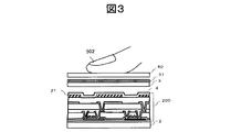
図1に示す液晶表示装置における、表示部の断面の一部を拡大した概略断面図を図3に示す。
図3に示すようにTFT基板2には画素部200が設けられており、対向電極21は画素の一部として画像表示に用いられる。また、TFT基板2とCF基板3との間には液晶組成物4が狭持されている。CF基板3に設けられた検出電極31とTFT基板に設けられた対向電極21とは容量を形成しており、対向電極21に駆動信号が印加されると検出電極31の電圧が変化する。
この時、図3に示すように、フロントウィンドウ40を介して指502等の導電体が近接または接触すると、容量に変化が生じ検出電極31に生じる電圧に、近接・接触が無い場合に比較して変化が生じる。
このように、液晶表示パネルに形成した対向電極21と検出電極31との間に生じる容量の変化を検出することで、液晶表示パネルにタッチパネルの機能を備えることが可能となる。
FIG. 3 shows a schematic cross-sectional view in which a part of the cross section of the display portion in the liquid crystal display device shown in FIG. 1 is enlarged.
As shown in FIG. 3, the
At this time, as shown in FIG. 3, when a conductor such as a
Thus, by detecting a change in capacitance generated between the
図4は、本発明の前提となるインセル方式の液晶表示装置における、タッチパネルの全体概略構成を示すブロック図である。
図4において、101はLCDドライバ、102はシーケンサ、103はタッチパネル走査電圧生成回路、106はデコーダ回路、107はタッチパネル、108は検出回路である。
タッチパネル107には、ユーザのタッチを検出するためのセンサ端子である電極パターン(TX0〜TX4の走査電極、RX0〜RX4の検出電極)が形成されている。
本発明の前提となるインセル方式の液晶表示装置は、タッチパネル機能が液晶表示パネルに内蔵されているため、図2に示す帯状の対向電極21が走査電極(TX)を兼用し、また、検出電極31が検出電極(RX)を構成する。
LCDドライバ101は、液晶表示パネルに画像を表示するための同期信号(垂直同期信号(Vsync)及び水平同期信号(Hsync))をシーケンサ102へ送出する。
シーケンサ102は、タッチパネル走査電圧生成回路103、デコーダ106、及び検出回路108を制御して、タッチ検出動作のタイミングを制御する。
タッチパネル走査電圧生成回路103は、TX0〜TX4の走査電極を駆動するためのタッチパネル走査電圧(Vstc)を生成して出力する。
デコーダ106は、シーケンサ102から入力される選択信号に基づいて、タッチパネル走査電圧(Vstc)を、TX0〜TX4の走査電極の中1つの走査電極へ出力するアナログスイッチ(デマルチプレクサ)である。
検出回路108は、TX0〜TX4の走査電極の中で、タッチパネル走査電圧(Vstc)が供給されている1つの走査電極と、RX0〜RX4の各検出電極との交点における電極間容量(相互容量)を検出する。
FIG. 4 is a block diagram showing an overall schematic configuration of the touch panel in the in-cell type liquid crystal display device as a premise of the present invention.
In FIG. 4, 101 is an LCD driver, 102 is a sequencer, 103 is a touch panel scanning voltage generation circuit, 106 is a decoder circuit, 107 is a touch panel, and 108 is a detection circuit.
On the
Since the in-cell type liquid crystal display device which is the premise of the present invention has a touch panel function built in the liquid crystal display panel, the strip-shaped
The
The
The touch panel scanning
The
The
図5は、本発明の前提となるインセル方式の液晶表示装置における、タッチパネルの検出原理を説明するための図である。
図6は、本発明の前提となるインセル方式の液晶表示装置における、タッチ検出動作のタイミング図である。
シーケンサ102は、タッチパネル走査電圧生成回路103等を制御し、垂直同期信号(Vsync)及び水平同期信号(Hsync)に同期しながら、TX0〜TX4の走査電極へ順次タッチパネル走査電圧(Vstc)を供給する。ここで、図5、図6に示すように、各走査電極には、タッチパネル走査電圧(Vstc)が複数回(図6では8回)供給される。
図6に示すように、検出回路108は、RX0〜RX4の各検出電極に流れる電流を積算し(図6では負方向への積算)、到達した電圧値(△Va,△Vb)を記録する。
走査電極(TX)と検出電極(RX)との交点付近を、指(導体)がタッチしている場合、指へも電流が流れるため、積算結果の電圧値に変化が生じる。
例えば、図6において、走査電極(TX0)と検出電極(RXn)との交点付近に指が存在しない場合(図6のNAに示すタッチ無しの状態)、検出電極に流れる電流を積算した電圧は、非タッチレベル(LA)となる。
これに対して、走査電極(TX2)と検出電極(RXn)との交点付近には指が存在する場合(図6のNBに示すタッチ有りの状態)、指へも電流が流れ、検出電極に流れる電流を積算した電圧は、非タッチレベル(LA)よりも高電位の電圧となる。この変化量(タッチ信号)によりタッチ位置を検出することができる。
FIG. 5 is a diagram for explaining the detection principle of the touch panel in the in-cell type liquid crystal display device as a premise of the present invention.
FIG. 6 is a timing chart of the touch detection operation in the in-cell type liquid crystal display device which is a premise of the present invention.
The
As shown in FIG. 6, the
When the finger (conductor) is touching the vicinity of the intersection of the scan electrode (TX) and the detection electrode (RX), a current flows also to the finger, so that the voltage value of the integration result changes.
For example, in FIG. 6, when a finger is not present near the intersection of the scan electrode (TX0) and the detection electrode (RXn) (without touch as indicated by NA in FIG. 6), the voltage obtained by integrating the current flowing through the detection electrode is It becomes a non-touch level (LA).
On the other hand, when a finger is present near the intersection of the scan electrode (TX2) and the detection electrode (RXn) (in a state with a touch indicated by NB in FIG. 6), a current also flows to the finger, The voltage obtained by integrating the flowing current is a voltage having a higher potential than the non-touch level (LA). The touch position can be detected from this change amount (touch signal).
図7は、本発明の前提となるインセル方式の液晶表示装置における、タッチパネル検出時と、画素書込み時のタイミングを説明するための図である。なお、図7において、T3は帰線期間、VSYNCは垂直同期信号、HSYNCは水平同期信号である
図7のAは、1フレームの画素書込み期間(T4)に、1番目の表示ラインから1280表示ラインまでの画素書込みタイミングを示し、図7のBが、20ブロックに分割された各ブロックの対向電極(CT1〜CT20)におけるタッチパネル検出タイミングを示す。
図7に示すように、任意の表示ラインの対向電極を走査電極(TX)として機能させ、タッチパネル検出時のスキャン動作は、画素書き込みを行うゲートスキャンとは異なる箇所で行う。
図7で説明したように、ゲートスキャンと、タッチパネル走査は異なる表示ラインで実施しているが、映像線と対向電極(CT)との間、および、走査線と対向電極(CT)との間には寄生容量があるため、映像線上の電圧(VDL)の変動、あるいは、走査電圧(VGL)の立ち上がり、あるいは、立ち下り時に生じるノイズにより、タッチパネル検出時の検出感度が低下する。
そこで、本発明の前提となるインセル方式の液晶表示装置では、タッチ位置検出動作は、映像線上の電圧(VDL)の変動、あるいは、走査電圧(VGL)の立ち上がり、あるいは、立ち下りがない期間に実行される。
FIG. 7 is a diagram for explaining the timing at the time of touch panel detection and pixel writing in the in-cell type liquid crystal display device as a premise of the present invention. In FIG. 7, T3 is a blanking period, VSYNC is a vertical synchronizing signal, and HSYNC is a horizontal synchronizing signal. FIG. 7A shows 1280 displays from the first display line in the pixel writing period (T4) of one frame. The pixel writing timing up to the line is shown, and B in FIG. 7 shows the touch panel detection timing in the counter electrodes (CT1 to CT20) of each block divided into 20 blocks.
As shown in FIG. 7, the counter electrode of an arbitrary display line is made to function as a scanning electrode (TX), and the scanning operation at the time of touch panel detection is performed at a location different from the gate scanning for pixel writing.
As described in FIG. 7, the gate scan and the touch panel scan are performed on different display lines, but between the video line and the counter electrode (CT) and between the scan line and the counter electrode (CT). Since there is a parasitic capacitance, the detection sensitivity at the time of touch panel detection decreases due to fluctuations in the voltage (VDL) on the video line, or noise generated at the rise or fall of the scanning voltage (VGL).
Therefore, in the in-cell type liquid crystal display device which is a premise of the present invention, the touch position detection operation is performed during a period when there is no fluctuation of the voltage (VDL) on the video line, or when the scanning voltage (VGL) rises or falls. Executed.
図8は、本発明の実施例のインセル方式の液晶表示装置の検出回路108のより具体的な回路構成を示す回路図である。
図9は、図8に示す回路の動作を説明するためのタイミングチャートである。
図8において、MPUはマイクロコンピュータ、CINTは積分容量、Cclbはキャリブレーション容量、10は積分回路、11はサンプルホールド回路、12は10ビットのAD変換器、13はAD変換器12から出力されるデータ(以下、Rawデータ)を格納する検出RAM、14はキャリブレーションRAM、15は8ビットのDA変換器、107はタッチパネル、108検出回路である。
以下、図9を用いて、本実施例の検出回路108の動作を説明する。なお、図9において、Hsyncは水平同期信号である。
(1)各検出電極(RX0〜RXn)に流れる電流を検出(積分)前に、スイッチ(S1)をオンして、積分回路10をリセットするとともに、スイッチ(S3)をオンとして、各検出電極(RX0〜RXn)をリセットする(図9のA1の期間)。基準電圧(VREF)を4V(VREF=4V)とすると、積分回路10の出力は4V、各検出電極(RX0〜RXn)は、4Vにプリチャージされる。
また、スイッチ(S5)は、基準電圧(VREF)側に接続されており、キャリブレーション容量(Cclb)の両端には、基準電圧(VREF)の4Vが印加されているため、キャリブレーション容量(Cclb)の電荷は「0」である。
FIG. 8 is a circuit diagram showing a more specific circuit configuration of the
FIG. 9 is a timing chart for explaining the operation of the circuit shown in FIG.
In FIG. 8, MPU is a microcomputer, CINT is an integration capacitor, Cclb is a calibration capacitor, 10 is an integration circuit, 11 is a sample and hold circuit, 12 is a 10-bit AD converter, and 13 is output from the
Hereinafter, the operation of the
(1) Before detecting (integrating) the current flowing through each detection electrode (RX0 to RXn), the switch (S1) is turned on to reset the
The switch (S5) is connected to the reference voltage (VREF) side, and 4 V of the reference voltage (VREF) is applied to both ends of the calibration capacitor (Cclb). ) Is “0”.
(2)次に、スイッチ(S1)とスイッチ(S3)をオフとした後、TX0〜TXmの走査電極の1つから、タッチパネル走査電圧(Vstc)を出力し、スイッチ(S5)を、DA変換器15側に切り替え、キャリブレーション容量(Cclb)の一端に、DA変換器15から出力されるキャリブレーション電圧(VDAC)を印加し、電荷の引き抜きを行った後に、スイッチ(S2)をオンとして残りの電荷を積分容量(CINT)に積分する(図9のB1の期間)。
これにより、TX0〜TXmの走査電極の1つ⇒交差容量(Cxy)⇒積分容量(CINT)の経路で電流が流れ、積分回路10の出力電圧(VINT)が低下する。
ここで、(交差容量(Cxy)の電荷)−(キャリブレーション容量(Cclb)の電荷)=積分容量(CINT)の電荷であり、
VINT=VREF−(Vstc*Cxy−Vclb*Cclb)/Cint
なお、Cintは積分容量(CINT)の容量値であり、また、Vclbは、キャリブレーション容量(Cclb)の両端に印加される電圧であり、(Vclb=VREF−VDAC)である。
(3)積分回路10での積分終了後、スイッチ(S2)をオフ、スイッチ(S3)をオンとし、かつ、スイッチ(S5)を基準電圧(VREF)側に接続して、各検出電極(RX0〜RXn)を4Vにプリチャージするとともに、キャリブレーション容量(Cclb)の電荷を「0」とする(図9のA2の期間)。
(2) Next, after turning off the switch (S1) and the switch (S3), the touch panel scanning voltage (Vstc) is output from one of the scanning electrodes TX0 to TXm, and the switch (S5) is converted to DA. After switching to the
As a result, a current flows through a path of one of the scan electrodes TX0 to TXm ⇒ cross capacitance (Cxy) ⇒ integration capacitance (CINT), and the output voltage (VINT) of the
Here, (the charge of the cross capacitor (Cxy)) − (the charge of the calibration capacitor (Cclb)) = the charge of the integration capacitor (CINT),
VINT = VREF− (Vstc * Cxy−Vclb * Cclb) / Cint
Cint is a capacitance value of the integration capacitor (CINT), and Vclb is a voltage applied to both ends of the calibration capacitor (Cclb), and is (Vclb = VREF−VDAC).
(3) After the integration in the integrating
(4)(2)の積分回路10での積分動作を繰り返し、電圧を積み上げる(図9のB2,…の期間)。
(5)積分回路10での積分完了後(図9のBnの期間後)、スイッチ(S4)をオンとして、サンプルホールド回路11でサンプル&ホールドし(図9のCの期間)、その後、スイッチ(S6)を順次オンとして、AD変換器13でAD変換し、検出RAM(13)に、RX0〜RXnの走査電極分のRawデータを格納する。
AD変換器12が、10bitのAD変換器の場合、Rawデータは0(積分0V)〜1023(積分4V)の範囲となる。
(6)(1)〜(5)の処理を、全ての走査電極(TX0〜TXm)について順次実行し、各走査電極(TX0〜TXm)と各検出電極(RX0〜RXn)の交点1面分のRawデータを検出RAM(13)に格納する。
(7)交差容量(Cxy)は非タッチ時>タッチ時であるので、図6のVa、Vbに示すように、積分回路10での積分出力電圧(VINT)の降下に差が生じ、ここにしきい値を設けて、タッチ検出する。
(4) The integration operation in the
(5) After the integration in the
When the
(6) The processes of (1) to (5) are sequentially executed for all the scan electrodes (TX0 to TXm), and one intersection point of each scan electrode (TX0 to TXm) and each detection electrode (RX0 to RXn). Are stored in the detection RAM (13).
(7) Since the cross capacitance (Cxy) is not touched> touched, as shown by Va and Vb in FIG. 6, a difference occurs in the drop in the integrated output voltage (VINT) in the integrating
図10は、本発明の実施例のインセル方式の液晶表示装置のタッチパネル107、検出RAM(13)、および、キャリブレーションRAM(14)のアドレスマップを示す図である。
同図(a)が、タッチパネル107のアドレスマップを、同図(b)が検出RAM(13)のアドレスマップを、同図(c)が後述するキャリブレーションRAM(14)のアドレスマップを示す。
図10に示すように、図10(a)に示す各走査電極(TX0〜TXm)と各検出電極(RX0〜RXn)の交点に対応する、積分回路10での積分出力電圧(VINT)をAD変換器12でAD変換し、交点1面分のRawデータを検出RAM(13)の当該交点のアドレス位置に格納する。
同様に、図10(a)に示す各走査電極(TX0〜TXm)と各検出電極(RX0〜RXn)の交点に対応するキャリブレーションデータを、キャリブレーションRAM(14)の当該交点のアドレス位置に格納する。
例えば、図10(a)に示すように、走査電極(TX0)と検出電極(RX0)の交点のアドレスが(0.0)の場合、走査電極(TX0)と検出電極(RX0)の交点の、積分回路10での積分出力電圧(VINT)は、検出RAM(13)の(0.0)のアドレス位置に格納され、走査電極(TX0)と検出電極(RX0)の交点のキャリブレーションデータは、キャリブレーションRAM(14)の(0.0)のアドレス位置に格納される。
FIG. 10 is a diagram showing an address map of the
3A shows an address map of the
As shown in FIG. 10, the integrated output voltage (VINT) in the integrating
Similarly, the calibration data corresponding to the intersections of the scanning electrodes (TX0 to TXm) and the detection electrodes (RX0 to RXn) shown in FIG. 10A are stored at the address position of the intersection of the calibration RAM (14). Store.
For example, as shown in FIG. 10A, when the address of the intersection of the scan electrode (TX0) and the detection electrode (RX0) is (0.0), the intersection of the scan electrode (TX0) and the detection electrode (RX0) The integration output voltage (VINT) in the
次に、キャリブレーションについて説明する。
前述したように、各走査電極(TX0〜TXm)と各検出電極(RX0〜RXn)の交点の交差容量(Cxy)は、液晶層、ガラス基板、偏光板、接着樹脂などの誘電率や厚みのばらつき、また不均一性のため、個体差や面内ばらつきを持つため、キャリブレーションが必須である。
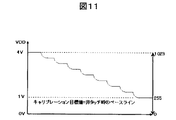
(7)図11に示すように、非タッチ時Rawデータ動作点を255とし、マイクロコンピュータ(MPU)は、これをキャリブレーション目標値として、キャリブレーションRAM(14)のキャリブレーションデータを書き換え、DA変換器15から出力されるキャリブレーション電圧(VDAC)を可変しながら収束させる。
なお、非タッチ時のRawデータ動作点とは、非タッチ時の積分回路10での積分出力電圧(VINT)を、サンプルホールド回路11でサンプル&ホールドし、10ビットのAD変換器12でAD変換したときのRawデータであることは言うまでもない。
(8)キャリブレーションは動作点を移動させる作用のみで、検出感度には影響しない。
検出感度=(△Cxy/Cint)*Vstc
△Cxy=Cxy_ut(非タッチ時の交差容量)−Cxy_t(タッチ時の交差容量)
なお、通常、キャリブレーション範囲が、8ビットで[8’h80]の付近、即ち、基準電圧(VREF;本実施例では、4V)とGND(0V)の電圧の中間付近の電圧となるように、キャリブレーション容量(Cclb)を決定する。また、通常、キャリブレーション容量(Cclb)は、ダイオード接続されたMOSトランジスタの接合容量を利用するので、キャリブレーション容量(Cclb)の増減は、ダイオード接続されたMOSトランジスタが、並列に接続される個数で調整する。
Next, calibration will be described.
As described above, the cross capacitance (Cxy) at the intersection of each scan electrode (TX0 to TXm) and each detection electrode (RX0 to RXn) is the dielectric constant or thickness of the liquid crystal layer, glass substrate, polarizing plate, adhesive resin, etc. Calibration is indispensable because there are individual differences and in-plane variations due to variations and non-uniformity.
(7) As shown in FIG. 11, the raw data operating point at the time of non-touch is set to 255, and the microcomputer (MPU) rewrites the calibration data of the calibration RAM (14) using this as a calibration target value, and DA The calibration voltage (VDAC) output from the
The raw data operating point at the time of non-touch means that the integration output voltage (VINT) at the
(8) Calibration is only an action of moving the operating point, and does not affect the detection sensitivity.
Detection sensitivity = (ΔCxy / Cint) * Vstc
ΔCxy = Cxy_ut (cross capacitance when not touched) −Cxy_t (cross capacitance when touched)
Normally, the calibration range is 8 bits and is in the vicinity of [8′h80], that is, a voltage in the vicinity of the middle between the reference voltage (VREF; 4V in this embodiment) and GND (0V). The calibration capacity (Cclb) is determined. In general, the calibration capacitor (Cclb) uses the junction capacitance of a diode-connected MOS transistor. Therefore, the calibration capacitor (Cclb) is increased or decreased by the number of diode-connected MOS transistors connected in parallel. Adjust with.
次に、互いに隣接する2つの検出電極がショートしているか否かの検査(以下、RX隣接ショート検査という)について説明する。
本実施例では、RX隣接ショート検査に、前述したキャリブレーション容量(Cclb)を利用する。
図12に示すように、RX隣接ショート検査時、キャリブレーションRAM(14)における、奇数番目の検出電極に対応するアドレス(図12のR0,R2,R4の列)には、電荷を引き抜かないキャリブレーションデータ(8ビットで[8’h00])を、キャリブレーションRAM(14)における、偶数番目の検出電極に対応するアドレス(図12のR1,R3,R5の列)には、十分に電荷を引き抜けるキャリブレーションデータ(8ビットで[8’hFF])を設定する。
キャリブレーションRAM(14)に、電荷を引き抜かないキャリブレーションデータ(8ビットで[8’h00])を設定すると、DA変換器15から出力されるキャリブレーション電圧(VDAC)は、基準電圧(VREF;本実施例では、4V)となり、キャリブレーションRAM(14)に、十分に電荷を引き抜けるキャリブレーションデータ(8ビットで[8’hFF])を設定すると、DA変換器15から出力されるキャリブレーション電圧(VDAC)は、GND(0V)付近の電圧となる。
Next, an inspection of whether or not two adjacent detection electrodes are short-circuited (hereinafter referred to as “RX adjacent short-circuit inspection”) will be described.
In the present embodiment, the above-described calibration capacitor (Cclb) is used for the RX adjacent short inspection.
As shown in FIG. 12, in the RX adjacent short inspection, the calibration RAM (14) does not extract charges at the addresses corresponding to the odd-numbered detection electrodes (rows R0, R2, and R4 in FIG. 12). To the address corresponding to the even-numbered detection electrodes (columns R1, R3, and R5 in FIG. 12) in the calibration RAM (14). Calibration data to be pulled out (8 bits [8′hFF]) is set.
When calibration data (8 bits [8'h00]) that does not extract charges is set in the calibration RAM (14), the calibration voltage (VDAC) output from the
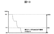
フレキシブル配線基板(図1(a)の53、図1(a)、(b)のMFPC)上の配線を含めて、互いに隣接する2つの検出電極が、RX隣接ショートしていない場合、奇数番目の検出電極(RX)に接続されるキャリブレーション容量(Cclb)の他端には、基準電圧(VREF)が印加されている。
そのため、走査電極(TX)から奇数番目の検出電極(RX)に流れる電流は、積分回路10に流れ、即ち、キャリブレーション容量(Cclb)での電荷の引き抜きがないので、積分回路10の積分容量(CINT)で積分され、図13に示すように、積分回路10の出力は、GNDに飽和する。
したがって、積分回路10での積分出力電圧(VINT)を、サンプルホールド回路11でサンプル&ホールドし、AD変換器12でAD変換したときのRawデータは、Raw=0となる。
また、互いに隣接する2つの検出電極が、RX隣接ショートしていない場合、偶数番目の検出電極(RX)に接続されるキャリブレーション容量(Cclb)の他端には、GND(0V)付近の電圧が印加されている。
そのため、走査電極(TX)から奇数番目の検出電極(RX)に流れる全ての電流はキャリブレーション容量(Cclb)に流れ、即ち、キャリブレーション容量(Cclb)により、全電荷が引き抜かれ、また、積分回路10の積分容量(CINT)からも電荷が移動し、積分回路10の積分出力電圧(VINT)は上昇し、図14に示すように、VDD(5V)に飽和する。
したがって、積分回路10での積分出力電圧(VINT)を、サンプルホールド回路11でサンプル&ホールドし、AD変換器12でAD変換したときのRawデータは、Raw=1023となる。
よって、図15(a)に示すように、検出RAM(13)に格納されるRawデータは、奇数番目の検出電極(RX)に対応する列が、10ビットで[1023]の値、偶数番目の検出電極(RX)に対応する列が、10ビットで[0]の値となる。
If the two adjacent detection electrodes including the wiring on the flexible wiring board (53 in FIG. 1 (a), MFPC in FIGS. 1 (a) and (b)) are not short adjacent to RX, the odd number A reference voltage (VREF) is applied to the other end of the calibration capacitor (Cclb) connected to the detection electrode (RX).
Therefore, the current that flows from the scan electrode (TX) to the odd-numbered detection electrode (RX) flows to the
Accordingly, the raw data when the integrated output voltage (VINT) in the integrating
In addition, when two adjacent detection electrodes are not short adjacent to RX, a voltage near GND (0 V) is applied to the other end of the calibration capacitor (Cclb) connected to the even-numbered detection electrode (RX). Is applied.
Therefore, all currents flowing from the scan electrode (TX) to the odd-numbered detection electrodes (RX) flow to the calibration capacitor (Cclb), that is, all charges are extracted by the calibration capacitor (Cclb), and integration is performed. The charge also moves from the integration capacitor (CINT) of the
Therefore, the raw data when the integrated output voltage (VINT) in the integrating
Therefore, as shown in FIG. 15A, the Raw data stored in the detection RAM (13) is 10 bits in the column corresponding to the odd-numbered detection electrode (RX), the value of [1023], the even-numbered number. The column corresponding to each detection electrode (RX) has a value of [0] with 10 bits.
一方、フレキシブル配線基板(図1(a)の53、図1(a)、(b)のMFPC)上の配線を含めて、互いに隣接する2つの検出電極が、RX隣接ショートしている場合、走査電極(TX)から奇数番目の検出電極(RX)に流れる全ての電流は、他端にGND(0V)付近の電圧が印加されている、偶数番目の検出電極(RX)に接続されるキャリブレーション容量(Cclb)に流れ、即ち、全電荷が引き抜かれ、また、積分回路10の積分容量(CINT)からも電荷が移動し、積分回路10の積分出力電圧(VINT)は上昇し、図14に示すように、VDD(5V)に飽和する。
したがって、積分回路10での積分出力電圧(VINT)を、サンプルホールド回路11でサンプル&ホールドし、AD変換器12でAD変換したときのRawデータは、Raw=1023となる。
よって、図15(b)に示すように、検出RAM(13)に格納されるRawデータの中で、RX隣接ショートしている、互いに隣接する2つの検出電極に対応する列のRawデータは、10ビットで[1023]の値となる。
このように、本実施例によれば、簡単かつ短時間にRX隣接ショート不良を検出することができる。
On the other hand, when two adjacent detection electrodes including the wiring on the flexible wiring board (53 in FIG. 1A, MFPC in FIG. 1A and FIG. 1B) are short adjacent to RX, All currents flowing from the scan electrode (TX) to the odd-numbered detection electrode (RX) are connected to the even-numbered detection electrode (RX), with the other end applied with a voltage in the vicinity of GND (0 V). 14, i.e., all charges are extracted, the charges are also transferred from the integration capacitor (CINT) of the
Therefore, the raw data when the integrated output voltage (VINT) in the integrating
Therefore, as shown in FIG. 15B, among the raw data stored in the detection RAM (13), the raw data in the columns corresponding to the two adjacent detection electrodes that are adjacent to each other in RX are short-circuited. The value of [1023] is 10 bits.
Thus, according to the present embodiment, it is possible to detect the RX adjacent short-circuit defect easily and in a short time.
なお、前述の説明から理解できるように、奇数番目の検出電極(RX)(または、偶数番目の検出電極(RX))に、スイッチ回路を介して、大きめの容量値を有する容量素子を接続し、かつ、GNDの電圧を出力する定電圧源を設け、RX隣接ショート検査に、スイッチ回路をオンとして、奇数番目の検出電極(RX)(または、偶数番目の検出電極(RX))に、他端に定電圧源からのGNDの電圧が印加されている容量素子を接続するようにしても、簡単かつ短時間にRX隣接ショート不良を検出することができる。
この時、フレキシブル配線基板(図1(a)の53、図1(a)、(b)のMFPC)上の配線を含めて、互いに隣接する2つの検出電極が、RX隣接ショートしていない場合は、検出RAM(13)に格納されるRawデータは、スイッチ回路を介して、大きめの容量値を有する容量素子を接続される検出電極(RX)に対応する列が、10ビットで[1023]の値、それ以外の検出電極(RX)に対応する列が、キャリブレーション終了後の非タッチレベルの、10ビットで[255]の値となる。
以上、本発明者によってなされた発明を、前記実施例に基づき具体的に説明したが、本発明は、前記実施例に限定されるものではなく、その要旨を逸脱しない範囲において種々変更可能であることは勿論である。
As can be understood from the above description, a capacitive element having a larger capacitance value is connected to the odd-numbered detection electrodes (RX) (or even-numbered detection electrodes (RX)) via a switch circuit. In addition, a constant voltage source that outputs the GND voltage is provided, the RX adjacent short test is performed, the switch circuit is turned on, the odd number detection electrode (RX) (or the even number detection electrode (RX)), etc. Even when a capacitive element to which the GND voltage from the constant voltage source is applied is connected to the end, the RX adjacent short circuit defect can be detected easily and in a short time.
At this time, when two adjacent detection electrodes including the wiring on the flexible wiring board (53 in FIG. 1A, MFPC in FIGS. 1A and 1B) are not short-circuited by RX In the Raw data stored in the detection RAM (13), the column corresponding to the detection electrode (RX) to which the capacitive element having a larger capacitance value is connected via the switch circuit is 10 bits [1023]. And the column corresponding to the other detection electrode (RX) have a value of [255] with 10 bits of the non-touch level after the calibration is completed.
As mentioned above, the invention made by the present inventor has been specifically described based on the above embodiments. However, the present invention is not limited to the above embodiments, and various modifications can be made without departing from the scope of the invention. Of course.
2 第1基板
3 第2基板
4 液晶組成物
5 液晶ドライバIC
10 積分回路
11 サンプルホールド回路
12 AD変換器
13 検出RAM
14 キャリブレーションRAM
15 DA変換器
21 対向電極
22 対向電極信号線
25 駆動回路用入力端子
31 検出電極
33 ダミー電極
36 検出電極用端子
40 フロントウィンドウ(又は、保護フィルム)
53 接続用フレキシブル配線基板
101 LCDドライバ
102 シーケンサ
103 タッチパネル走査電圧生成回路
106 デコーダ回路
107 タッチパネル
108 検出回路
200 画素部
502 指
MPU マイクロコンピュータ
MFPC メインフレキシブル配線基板
TX タッチパネルの走査電極
RX タッチパネルの検出電極
2
DESCRIPTION OF
14 Calibration RAM
15
53 Flexible wiring board for
Claims (6)
第2基板と、
前記第1基板と前記第2基板との間に狭持される液晶とを有する液晶表示パネルを備え、マトリクス状に配置された複数の画素を有する液晶表示装置であって、
前記第2基板は、タッチパネルの検出電極を有し、
前記各画素は、画素電極と対向電極とを有し、
前記対向電極には画像表示に用いられる対向電圧と、タッチ位置の検出に用いられるタッチパネル走査電圧が印加され、
前記対向電極は、複数のブロックに分割されており、
前記分割された各ブロックの対向電極は、連続する複数の表示ラインの各画素に対して共通に設けられており、
前記分割された各ブロックの対向電極は、前記タッチパネルの走査電極を兼用し、
前記各検出電極毎に設けられ、一端が前記各検出電極に接続されるキャリブレーション容量素子を有し、
タッチ位置検出処理前に、前記検出電極に基準電圧がプリチャージされて、キャリブレーション容量素子の前記一端に基準電圧が印加され、かつ、前記キャリブレーション容量素子の他端に基準電圧が印加され、
タッチ位置検出処理時に、前記タッチパネルの走査電極となる対向電極には、前記タッチパネル走査電圧が印加され、
かつ、前記各キャリブレーション容量素子の前記他端にキャリブレーション電圧を供給する手段を有することを特徴とする液晶表示装置。 A first substrate;
A second substrate;
A liquid crystal display device comprising a liquid crystal display panel having a liquid crystal sandwiched between the first substrate and the second substrate, and having a plurality of pixels arranged in a matrix,
The second substrate has a touch panel detection electrode;
Each of the pixels has a pixel electrode and a counter electrode,
A counter voltage used for image display and a touch panel scanning voltage used for detection of a touch position are applied to the counter electrode,
The counter electrode is divided into a plurality of blocks,
The counter electrode of each of the divided blocks is provided in common for each pixel of a plurality of continuous display lines,
The counter electrode of each divided block also serves as the scan electrode of the touch panel,
It is provided for each of the detection electrodes, and has a calibration capacitance element having one end connected to each of the detection electrodes,
Before the touch position detection process, a reference voltage is precharged to the detection electrode, a reference voltage is applied to the one end of the calibration capacitive element, and a reference voltage is applied to the other end of the calibration capacitive element,
During the touch position detection process, the touch panel scanning voltage is applied to the counter electrode that becomes the scanning electrode of the touch panel,
And, a liquid crystal display device characterized by having a means for supplying a calibration voltage to the other end of said each calibration capacitor element.
第2基板と、
前記第1基板と前記第2基板との間に教示される液晶とを有する液晶表示パネルを備え、マトリクス状に配置された複数の画素を有する液晶表示装置であって、
前記第2基板は、タッチパネルの検出電極を有し、
前記各画素は、画素電極と対向電極とを有し、
前記対向電極は、複数のブロックに分割されており、
前記分割された各ブロックの対向電極は、連続する複数の表示ラインの各画素に対して共通に設けられており、
前記分割された各ブロックの対向電極は、前記タッチパネルの走査電極を兼用し、前記各ブロックの対向電極には画像表示に用いられる対向電圧と、タッチ位置の検出に用いられるタッチパネル走査電圧が印加され、
前記各検出電極毎に設けられ、一端が前記各検出電極に接続されるキャリブレーション容量素子と、
前記各検出電極と前記分割された各ブロックの対向電極との交点毎のキャリブレーションデータを記憶するメモリ素子とを有し、
タッチ位置検出処理前に、前記検出電極に基準電圧がプリチャージされて、キャリブレーション容量素子の前記一端に基準電圧が印加され、かつ、前記キャリブレーション容量素子の他端に基準電圧が印加され、
タッチ位置検出処理時に、前記タッチパネルの走査電極となる対向電極には、前記タッチパネル走査電圧が印加され、前記メモリ素子に記憶されたキャリブレーションデータに対応するキャリブレーションデータ電圧を生成し、対応するキャリブレーション容量素子の前記他端に供給する手段とを有することを特徴とする液晶表示装置。 A first substrate;
A second substrate;
A liquid crystal display device comprising a liquid crystal display panel having a liquid crystal taught between the first substrate and the second substrate, and having a plurality of pixels arranged in a matrix,
The second substrate has a touch panel detection electrode;
Each of the pixels has a pixel electrode and a counter electrode,
The counter electrode is divided into a plurality of blocks,
The counter electrode of each of the divided blocks is provided in common for each pixel of a plurality of continuous display lines,
The counter electrode of each divided block also serves as the scan electrode of the touch panel, and a counter voltage used for image display and a touch panel scan voltage used for detection of the touch position are applied to the counter electrode of each block. ,
A calibration capacitance element provided for each of the detection electrodes, one end of which is connected to each of the detection electrodes;
And a memory device for storing calibration data for each intersection of the opposing electrode of each block the is the divided respective detection electrodes,
Before the touch position detection process, a reference voltage is precharged to the detection electrode, a reference voltage is applied to the one end of the calibration capacitive element, and a reference voltage is applied to the other end of the calibration capacitive element,
During the touch position detection process, the touch panel scanning voltage is applied to the counter electrode serving as the scanning electrode of the touch panel, and a calibration data voltage corresponding to the calibration data stored in the memory element is generated, and the corresponding calibration is performed. the liquid crystal display device characterized by having means for supplying to said other end of the Deployment capacitive element.
第2基板と、
前記第1基板と前記第2基板との間に狭持される液晶とを有する液晶表示パネルを備え、マトリクス状に配置された複数の画素を有する液晶表示装置であって、
前記第2基板は、タッチパネルの検出電極を有し、
前記各画素は、画素電極と対向電極とを有し、
前記対向電極は、複数のブロックに分割されており、
前記分割された各ブロックの対向電極は、連続する複数の表示ラインの各画素に対して共通に設けられており、
前記分割された各ブロックの対向電極は、前記タッチパネルの走査電極を兼用し、前記各ブロックの対向電極には画像表示に用いられる対向電圧と、タッチ位置の検出に用いられるタッチパネル走査電圧が印加され、
前記各検出電極毎に設けられ、一端が前記各検出電極に接続されるキャリブレーション容量素子を有し、
タッチ位置検出処理前に、
前記検出電極に基準電圧がプリチャージされて、キャリブレーション容量の前記一端に基準電圧が印加され、かつ、前記キャリブレーション容量の他端に基準電圧が印加され、
タッチ位置検出処理時に、
前記走査電極には、タッチパネル走査電圧が印加され、
かつ、前記各キャリブレーション容量素子の前記他端にキャリブレーション電圧を供給してタッチ位置を検出し、
互いに隣接する2つの検出電極の短絡試験時に、一端が奇数列の検出電極に接続されるキャリブレーション容量素子の他端に電荷が引き抜かれないキャリブレーション電圧Aを供給し、一端が偶数列の検出電極に接続されるキャリブレーション容量素子の他端に充分に電荷を引き抜けるキャリブレーション電圧Bを供給し、タッチ位置検出処理を実行する手段を有することを特徴とする液晶表示装置。 A first substrate;
A second substrate;
A liquid crystal display device comprising a liquid crystal display panel having a liquid crystal sandwiched between the first substrate and the second substrate, and having a plurality of pixels arranged in a matrix,
The second substrate has a touch panel detection electrode;
Each of the pixels has a pixel electrode and a counter electrode,
The counter electrode is divided into a plurality of blocks,
The counter electrode of each of the divided blocks is provided in common for each pixel of a plurality of continuous display lines,
The counter electrode of each divided block also serves as the scan electrode of the touch panel, and a counter voltage used for image display and a touch panel scan voltage used for detection of the touch position are applied to the counter electrode of each block. ,
It is provided for each of the detection electrodes, and has a calibration capacitance element having one end connected to each of the detection electrodes,
Before the touch position detection process
A reference voltage is precharged to the detection electrode, a reference voltage is applied to the one end of the calibration capacitor, and a reference voltage is applied to the other end of the calibration capacitor,
During the touch position detection process,
A touch panel scanning voltage is applied to the scanning electrode,
And, a calibration voltage is supplied to the other end of each calibration capacitive element to detect a touch position,
During a short-circuit test of two adjacent detection electrodes, a calibration voltage A is supplied to the other end of the calibration capacitor element, one end of which is connected to the odd number of detection electrodes, and one end of the even number detection A liquid crystal display device comprising means for performing a touch position detection process by supplying a calibration voltage B that sufficiently draws out charges to the other end of a calibration capacitor connected to an electrode.
第2基板と、
前記第1基板と前記第2基板との間に狭持される液晶とを有する液晶表示パネルを備え、マトリクス状に配置された複数の画素を有する液晶表示装置であって、
前記第2基板は、タッチパネルの検出電極を有し、
前記各画素は、画素電極と対向電極とを有し、
前記対向電極は、複数のブロックに分割されており、
前記分割された各ブロックの対向電極は、連続する複数の表示ラインの各画素に対して共通に設けられており、
前記分割された各ブロックの対向電極は、前記タッチパネルの走査電極を兼用し、前記各ブロックの対向電極には画像表示に用いられる対向電圧と、タッチ位置の検出に用いられるタッチパネル走査電圧が印加され、
前記各検出電極毎に設けられ、一端が前記各検出電極に接続されるキャリブレーション容量素子と、
前記各検出電極と前記分割された各ブロックの対向電極との交点毎のキャリブレーションデータを記憶するメモリ素子とを有し、
タッチ位置検出処理前に、
前記検出電極に基準電圧がプリチャージされて、キャリブレーション容量の前記一端に基準電圧が印加され、かつ、前記キャリブレーション容量の他端に基準電圧が印加され、
タッチ位置検出処理時に、
前記走査電極には、タッチパネル走査電圧が印加され、
かつ、前記各キャリブレーション容量素子の前記他端にキャリブレーション電圧を供給してタッチ位置を検出し、
互いに隣接する2つの検出電極の短絡試験時に、奇数列の検出電極と前記分割された各ブロックの対向電極との交点毎のキャリブレーションデータとして、電荷が引き抜かれないキャリブレーションデータAを記憶し、偶数列の検出電極と前記分割された各ブロックの対向電極との交点毎のキャリブレーションデータとして、充分に電荷を引き抜けるキャリブレーションデータBを記憶し、
前記互いに隣接する2つの検出電極の短絡試験時に、前記メモリ素子に記憶されたキャリブレーションデータAに対応するキャリブレーションデータ電圧Aを生成して、一端が奇数列の検出電極に接続されるキャリブレーション容量素子の他端に供給するとともに、
前記メモリ素子に記憶されたキャリブレーションデータBに対応するキャリブレーションデータ電圧Bを生成して、一端が偶数列の検出電極に接続されるキャリブレーション容量素子の他端に供給し、タッチ位置検出処理を実行する手段を有することを特徴とする液晶表示装置。 A first substrate;
A second substrate;
A liquid crystal display device comprising a liquid crystal display panel having a liquid crystal sandwiched between the first substrate and the second substrate, and having a plurality of pixels arranged in a matrix,
The second substrate has a touch panel detection electrode;
Each of the pixels has a pixel electrode and a counter electrode,
The counter electrode is divided into a plurality of blocks,
The counter electrode of each of the divided blocks is provided in common for each pixel of a plurality of continuous display lines,
The counter electrode of each divided block also serves as the scan electrode of the touch panel, and a counter voltage used for image display and a touch panel scan voltage used for detection of the touch position are applied to the counter electrode of each block. ,
A calibration capacitance element provided for each of the detection electrodes, one end of which is connected to each of the detection electrodes;
A memory element that stores calibration data for each intersection of the detection electrodes and the counter electrodes of the divided blocks;
Before the touch position detection process
A reference voltage is precharged to the detection electrode, a reference voltage is applied to the one end of the calibration capacitor, and a reference voltage is applied to the other end of the calibration capacitor,
During the touch position detection process,
A touch panel scanning voltage is applied to the scanning electrode,
And, a calibration voltage is supplied to the other end of each calibration capacitive element to detect a touch position,
In a short-circuit test between two detection electrodes adjacent to each other, calibration data A in which charges are not extracted is stored as calibration data for each intersection point between the odd-numbered detection electrodes and the counter electrode of each of the divided blocks. As calibration data for each intersection of the even number of detection electrodes and the counter electrode of each of the divided blocks, calibration data B for sufficiently extracting charges is stored,
A calibration data voltage A corresponding to the calibration data A stored in the memory element is generated at the time of a short circuit test of the two adjacent detection electrodes, and one end is connected to the odd number of detection electrodes. While supplying to the other end of the capacitive element,
A calibration data voltage B corresponding to the calibration data B stored in the memory element is generated, and one end is supplied to the other end of the calibration capacitor element connected to the detection electrode in the even-numbered column to perform touch position detection processing. A liquid crystal display device comprising means for executing
第2基板と、
前記第1基板と前記第2基板との間に狭持される液晶とを有する液晶表示パネルを備え、マトリクス状に配置された複数の画素を有する液晶表示装置であって、
前記第2基板は、タッチパネルの検出電極を有し、
前記各画素は、画素電極と対向電極とを有し、
前記対向電極は、複数のブロックに分割されており、
前記分割された各ブロックの対向電極は、連続する複数の表示ラインの各画素に対して共通に設けられており、
前記分割された各ブロックの対向電極は、前記タッチパネルの走査電極を兼用し、前記各ブロックの対向電極には画像表示に用いられる対向電圧と、タッチ位置の検出に用いられるタッチパネル走査電圧が印加され、
前記各検出電極毎に設けられ、前記各検出電極に接続される複数の積分回路と、
前記各検出電極毎に設けられ、一端が前記各検出電極に接続されるキャリブレーション容量素子と、
前記各検出電極と前記分割された各ブロックの対向電極との交点毎のキャリブレーションデータを記憶するメモリ素子とを有し、
タッチ位置検出処理前に、
前記検出電極に基準電圧がプリチャージされて、キャリブレーション容量の前記一端に基準電圧が印加され、かつ、前記キャリブレーション容量の他端に基準電圧が印加され、
タッチ位置検出処理時に、
前記走査電極には、タッチパネル走査電圧が印加され、
かつ、前記各キャリブレーション容量素子の前記他端にキャリブレーション電圧を供給してタッチ位置を検出し、
互いに隣接する2つの検出電極の短絡試験時に、奇数列の検出電極と前記分割された各ブロックの対向電極との交点毎のキャリブレーションデータとして、電荷が引き抜かれないキャリブレーションデータAを記憶し、偶数列の検出電極と前記分割された各ブロックの対向電極との交点毎のキャリブレーションデータとして、充分に電荷を引き抜けるキャリブレーションデータBを記憶し、
前記互いに隣接する2つの検出電極の短絡試験時に、前記メモリ素子に記憶されたキャリブレーションデータAに対応するキャリブレーションデータ電圧Aとして、VREFの基準電圧を生成して、一端が奇数列の検出電極に接続されるキャリブレーション容量素子の他端に供給するとともに、前記メモリ素子に記憶されたキャリブレーションデータBに対応するキャリブレーションデータ電圧Bとして、前記各積分回路に供給されるGNDの電圧を生成して、一端が偶数列の検出電極に接続されるキャリブレーション容量素子の他端に供給し、タッチ位置検出処理を実行する手段を有することを特徴とする液晶表示装置。 A first substrate;
A second substrate;
A liquid crystal display device comprising a liquid crystal display panel having a liquid crystal sandwiched between the first substrate and the second substrate, and having a plurality of pixels arranged in a matrix,
The second substrate has a touch panel detection electrode;
Each of the pixels has a pixel electrode and a counter electrode,
The counter electrode is divided into a plurality of blocks,
The counter electrode of each of the divided blocks is provided in common for each pixel of a plurality of continuous display lines,
The counter electrode of each divided block also serves as the scan electrode of the touch panel, and a counter voltage used for image display and a touch panel scan voltage used for detection of the touch position are applied to the counter electrode of each block. ,
A plurality of integration circuits provided for each of the detection electrodes and connected to the detection electrodes;
A calibration capacitance element provided for each of the detection electrodes, one end of which is connected to each of the detection electrodes;
A memory element that stores calibration data for each intersection of the detection electrodes and the counter electrodes of the divided blocks;
Before the touch position detection process
A reference voltage is precharged to the detection electrode, a reference voltage is applied to the one end of the calibration capacitor, and a reference voltage is applied to the other end of the calibration capacitor,
During the touch position detection process,
A touch panel scanning voltage is applied to the scanning electrode,
And, a calibration voltage is supplied to the other end of each calibration capacitive element to detect a touch position,
In a short-circuit test between two detection electrodes adjacent to each other, calibration data A in which charges are not extracted is stored as calibration data for each intersection point between the odd-numbered detection electrodes and the counter electrode of each of the divided blocks. As calibration data for each intersection of the even number of detection electrodes and the counter electrode of each of the divided blocks, calibration data B for sufficiently extracting charges is stored,
During a short-circuit test of the two adjacent detection electrodes, a reference voltage of VREF is generated as a calibration data voltage A corresponding to the calibration data A stored in the memory element, and one end of the detection electrode is an odd number column Is supplied to the other end of the calibration capacitor element connected to, and generates a GND voltage supplied to each integration circuit as a calibration data voltage B corresponding to the calibration data B stored in the memory element. Then, a liquid crystal display device having means for supplying one end to the other end of the calibration capacitive element connected to the detection electrode in the even-numbered column and executing touch position detection processing.
前記各検出電極にVREFの基準電圧を供給する第2のスイッチ回路と、
前記各キャリブレーション容量素子の他端に、キャリブレーションデータ電圧あるいはVREFの基準電圧を供給する第3のスイッチ回路とを有し、
前記分割された各ブロックの対向電極にタッチパネル走査電圧を供給する前に、前記第1のスイッチ回路をオフ、前記第2のスイッチ回路をオンとし、前記第3のスイッチ回路により前記各キャリブレーション容量素子の他端に前記VREFの基準電圧を供給し、
前記分割された各ブロックの対向電極にタッチパネル走査電圧を供給している時に、前記第1のスイッチ回路をオン、前記第2のスイッチ回路をオフとし、前記第3のスイッチ回路により前記各キャリブレーション容量素子の他端に前記キャリブレーションデータ電圧を供給することを特徴とする請求項5に記載の液晶表示装置。 A first switch circuit connected between each detection electrode and each integration circuit;
A second switch circuit for supplying a reference voltage of VREF to each of the detection electrodes;
A third switch circuit for supplying a calibration data voltage or a VREF reference voltage to the other end of each calibration capacitor;
Before supplying the touch panel scanning voltage to the counter electrode of each of the divided blocks, the first switch circuit is turned off, the second switch circuit is turned on, and each calibration capacitor is turned on by the third switch circuit. Supplying the reference voltage of VREF to the other end of the element;
When the touch panel scanning voltage is supplied to the counter electrode of each of the divided blocks, the first switch circuit is turned on, the second switch circuit is turned off, and each calibration is performed by the third switch circuit. The liquid crystal display device according to claim 5, wherein the calibration data voltage is supplied to the other end of the capacitive element.
Priority Applications (9)
| Application Number | Priority Date | Filing Date | Title |
|---|---|---|---|
| JP2012267279A JP6035132B2 (en) | 2012-12-06 | 2012-12-06 | Liquid crystal display |
| TW102141321A TWI533186B (en) | 2012-12-06 | 2013-11-13 | Liquid crystal display device |
| TW105106547A TWI604365B (en) | 2012-12-06 | 2013-11-13 | Touch panel detection circuit |
| EP13195526.2A EP2741185A3 (en) | 2012-12-06 | 2013-12-03 | Liquid crystal display device |
| US14/094,991 US9535278B2 (en) | 2012-12-06 | 2013-12-03 | Liquid crystal display device |
| KR1020130149143A KR101545061B1 (en) | 2012-12-06 | 2013-12-03 | Liquid crystal display device |
| CN201310652179.4A CN103852921B (en) | 2012-12-06 | 2013-12-05 | Liquid crystal display device |
| CN201710333145.7A CN106932946B (en) | 2012-12-06 | 2013-12-05 | Display device |
| US15/178,846 US10180590B2 (en) | 2012-12-06 | 2016-06-10 | Liquid crystal display device |
Applications Claiming Priority (1)
| Application Number | Priority Date | Filing Date | Title |
|---|---|---|---|
| JP2012267279A JP6035132B2 (en) | 2012-12-06 | 2012-12-06 | Liquid crystal display |
Related Child Applications (1)
| Application Number | Title | Priority Date | Filing Date |
|---|---|---|---|
| JP2016212716A Division JP6255461B2 (en) | 2016-10-31 | 2016-10-31 | Liquid crystal display |
Publications (3)
| Publication Number | Publication Date |
|---|---|
| JP2014115708A JP2014115708A (en) | 2014-06-26 |
| JP2014115708A5 JP2014115708A5 (en) | 2016-01-21 |
| JP6035132B2 true JP6035132B2 (en) | 2016-11-30 |
Family
ID=49683611
Family Applications (1)
| Application Number | Title | Priority Date | Filing Date |
|---|---|---|---|
| JP2012267279A Active JP6035132B2 (en) | 2012-12-06 | 2012-12-06 | Liquid crystal display |
Country Status (6)
| Country | Link |
|---|---|
| US (2) | US9535278B2 (en) |
| EP (1) | EP2741185A3 (en) |
| JP (1) | JP6035132B2 (en) |
| KR (1) | KR101545061B1 (en) |
| CN (2) | CN106932946B (en) |
| TW (2) | TWI533186B (en) |
Families Citing this family (26)
| Publication number | Priority date | Publication date | Assignee | Title |
|---|---|---|---|---|
| JP6037327B2 (en) * | 2012-09-24 | 2016-12-07 | 株式会社ジャパンディスプレイ | Liquid crystal display |
| KR101681305B1 (en) * | 2014-08-01 | 2016-12-02 | 주식회사 하이딥 | Touch input device |
| KR101452302B1 (en) | 2013-07-29 | 2014-10-22 | 주식회사 하이딥 | Touch sensor panel |
| KR101712346B1 (en) | 2014-09-19 | 2017-03-22 | 주식회사 하이딥 | Touch input device |
| JP6205312B2 (en) | 2014-06-18 | 2017-09-27 | 株式会社ジャパンディスプレイ | Liquid crystal display |
| JP6527343B2 (en) | 2014-08-01 | 2019-06-05 | 株式会社 ハイディープHiDeep Inc. | Touch input device |
| WO2016136293A1 (en) * | 2015-02-27 | 2016-09-01 | シャープ株式会社 | Touch panel control substrate inspection method, and touch panel controller |
| TWI576735B (en) * | 2015-06-08 | 2017-04-01 | 群創光電股份有限公司 | Touch display panel and test method thereof |
| CN105068695A (en) * | 2015-09-11 | 2015-11-18 | 京东方科技集团股份有限公司 | Touch display panel with pressure detection function, display device and driving method |
| TWI684118B (en) * | 2015-09-22 | 2020-02-01 | 瀚宇彩晶股份有限公司 | Display device with pressure sensing |
| CN106610750B (en) * | 2015-10-21 | 2019-04-09 | 敦泰电子股份有限公司 | Touch control display device and its driving method |
| JP2017097551A (en) * | 2015-11-20 | 2017-06-01 | 株式会社ジャパンディスプレイ | Display device and manufacturing method of the same |
| CN108475154B (en) * | 2016-01-20 | 2022-04-05 | 谱瑞科技股份有限公司 | Integrated touch sensing and force sensing in touch detection device |
| TWI610207B (en) * | 2016-09-01 | 2018-01-01 | 凌巨科技股份有限公司 | Inspection method |
| JP6652901B2 (en) | 2016-09-16 | 2020-02-26 | 株式会社ジャパンディスプレイ | Display device and method of manufacturing the same |
| CN106484190A (en) * | 2016-11-18 | 2017-03-08 | 业成科技(成都)有限公司 | Touch module |
| KR102573208B1 (en) * | 2016-11-30 | 2023-08-30 | 엘지디스플레이 주식회사 | Display panel |
| KR102634473B1 (en) | 2016-12-23 | 2024-02-06 | 주식회사 엘엑스세미콘 | Panel driving device and display device |
| US10671214B2 (en) * | 2017-04-12 | 2020-06-02 | Synaptics Incorporated | Global coarse baseline correction charge injection |
| CN107561760A (en) * | 2017-09-19 | 2018-01-09 | 惠科股份有限公司 | Embedded touch display device |
| TWI626579B (en) * | 2017-12-06 | 2018-06-11 | 友達光電股份有限公司 | Display panel |
| US10521045B2 (en) * | 2018-02-14 | 2019-12-31 | Microchip Technology Incorporated | Reference noise rejection improvement based on sample and hold circuitry |
| CN110471225B (en) * | 2019-08-21 | 2022-06-21 | 合肥联宝信息技术有限公司 | Screen and liquid crystal calibration method |
| US11327602B2 (en) * | 2020-05-15 | 2022-05-10 | Chengdu Boe Optoelectronics Technology Co., Ltd. | Touch driving method, touch display device, and electronic device |
| JP7423428B2 (en) * | 2020-06-05 | 2024-01-29 | シャープ株式会社 | touch panel input device |
| CN113514673B (en) * | 2021-09-14 | 2022-01-28 | 苏州华兴源创科技股份有限公司 | Touch channel switching circuit, device and detection system |
Family Cites Families (23)
| Publication number | Priority date | Publication date | Assignee | Title |
|---|---|---|---|---|
| KR100494685B1 (en) * | 2000-12-30 | 2005-06-13 | 비오이 하이디스 테크놀로지 주식회사 | Method for testing defect of lcd panel wiring |
| GB2419950A (en) * | 2004-11-09 | 2006-05-10 | Sharp Kk | Capacitance measuring apparatus for LCD touch screen |
| KR101213102B1 (en) * | 2006-04-28 | 2012-12-18 | 엘지디스플레이 주식회사 | reflective and transflective liquid crystal display |
| KR101371604B1 (en) * | 2007-11-26 | 2014-03-06 | 삼성디스플레이 주식회사 | Liquid crystal display |
| JP4881331B2 (en) * | 2008-01-29 | 2012-02-22 | 株式会社東海理化電機製作所 | Touch switch |
| JP5481040B2 (en) * | 2008-04-11 | 2014-04-23 | 株式会社ジャパンディスプレイ | Display device and driving method thereof |
| JP5379790B2 (en) * | 2008-04-28 | 2013-12-25 | シャープ株式会社 | Active matrix substrate, liquid crystal display panel including the same, and method of manufacturing active matrix substrate |
| CN101308306B (en) | 2008-07-15 | 2011-03-16 | 友达光电股份有限公司 | Liquid crystal display device possessing testing structure and related test method |
| KR20100015225A (en) * | 2008-08-04 | 2010-02-12 | 삼성전자주식회사 | Liquid crystal display apparatus and touch sensing method thereof |
| JP5033078B2 (en) * | 2008-08-06 | 2012-09-26 | 株式会社ジャパンディスプレイイースト | Display device |
| KR101322957B1 (en) * | 2008-10-10 | 2013-10-29 | 엘지디스플레이 주식회사 | Touch sensor and driving method thereof |
| JP2010108501A (en) | 2008-10-30 | 2010-05-13 | Samsung Electronics Co Ltd | Touch screen controller having increased sensing sensitivity, and display driving circuit and display device and system having the touch screen controller |
| KR100935503B1 (en) * | 2009-01-28 | 2010-01-06 | 이성호 | Touch panel |
| JP5334197B2 (en) * | 2009-12-15 | 2013-11-06 | 株式会社ジャパンディスプレイ | Capacitance input device, inspection method for capacitance input device, drive device for capacitance input device |
| KR20110091380A (en) * | 2010-02-05 | 2011-08-11 | 삼성전자주식회사 | Method and apparatus for noise compensation in touch panel |
| JP5454267B2 (en) * | 2010-03-18 | 2014-03-26 | ソニー株式会社 | Detection device and display device |
| US9391607B2 (en) * | 2010-04-22 | 2016-07-12 | Qualcomm Technologies, Inc. | Use of random sampling technique to reduce finger-coupled noise |
| US8599167B2 (en) * | 2010-04-22 | 2013-12-03 | Maxim Integrated Products, Inc. | Method and apparatus for improving dynamic range of a touchscreen controller |
| JP5523191B2 (en) * | 2010-04-30 | 2014-06-18 | 株式会社ジャパンディスプレイ | Display device with touch detection function |
| US8860432B2 (en) | 2011-02-25 | 2014-10-14 | Maxim Integrated Products, Inc. | Background noise measurement and frequency selection in touch panel sensor systems |
| JP5822526B2 (en) * | 2011-05-09 | 2015-11-24 | シナプティクス・ディスプレイ・デバイス合同会社 | Touch detection device and semiconductor device |
| JP5685512B2 (en) * | 2011-09-29 | 2015-03-18 | 株式会社ジャパンディスプレイ | Display device, touch detection device, driving method, and electronic device |
| US9921691B2 (en) * | 2012-05-18 | 2018-03-20 | Atmel Corporation | Burst-mode self-capacitance measurement with compensated capacitance |
-
2012
- 2012-12-06 JP JP2012267279A patent/JP6035132B2/en active Active
-
2013
- 2013-11-13 TW TW102141321A patent/TWI533186B/en active
- 2013-11-13 TW TW105106547A patent/TWI604365B/en active
- 2013-12-03 EP EP13195526.2A patent/EP2741185A3/en not_active Withdrawn
- 2013-12-03 US US14/094,991 patent/US9535278B2/en active Active
- 2013-12-03 KR KR1020130149143A patent/KR101545061B1/en active IP Right Grant
- 2013-12-05 CN CN201710333145.7A patent/CN106932946B/en active Active
- 2013-12-05 CN CN201310652179.4A patent/CN103852921B/en active Active
-
2016
- 2016-06-10 US US15/178,846 patent/US10180590B2/en active Active
Also Published As
| Publication number | Publication date |
|---|---|
| US20140160371A1 (en) | 2014-06-12 |
| EP2741185A2 (en) | 2014-06-11 |
| KR20140073431A (en) | 2014-06-16 |
| TW201626198A (en) | 2016-07-16 |
| TW201423543A (en) | 2014-06-16 |
| CN103852921B (en) | 2017-05-24 |
| TWI604365B (en) | 2017-11-01 |
| EP2741185A3 (en) | 2016-07-20 |
| US10180590B2 (en) | 2019-01-15 |
| TWI533186B (en) | 2016-05-11 |
| CN106932946B (en) | 2021-03-30 |
| KR101545061B1 (en) | 2015-08-17 |
| CN103852921A (en) | 2014-06-11 |
| CN106932946A (en) | 2017-07-07 |
| US20160283039A1 (en) | 2016-09-29 |
| JP2014115708A (en) | 2014-06-26 |
| US9535278B2 (en) | 2017-01-03 |
Similar Documents
| Publication | Publication Date | Title |
|---|---|---|
| JP6035132B2 (en) | Liquid crystal display | |
| KR101350874B1 (en) | Display device and driving method thereof | |
| US9727163B2 (en) | Touch detection device, display device with touch detection function, and electronic apparatus | |
| JP6211409B2 (en) | Display device | |
| JP4957597B2 (en) | Sensing circuit, driving method thereof, display device, and electronic device | |
| JP6037327B2 (en) | Liquid crystal display | |
| US20140132526A1 (en) | Display device including integrated touch panel | |
| US8928599B2 (en) | Touch sensor using capacitance detection and liquid crystal display having the same | |
| JP2009301545A (en) | Touch screen display device | |
| KR20100008668A (en) | Touch sensor and liquid crystal display having the same | |
| JP6022320B2 (en) | Liquid crystal display | |
| JP5243069B2 (en) | Display device and electronic device | |
| KR102440812B1 (en) | Touch sensing apparatus and driving method thereof | |
| JP6255461B2 (en) | Liquid crystal display | |
| JP2009301006A (en) | Liquid crystal display device, and driving method and electronic device thereof | |
| JP2012168571A (en) | Capacitance change detection circuit and display device | |
| KR20170003806A (en) | Touch sensing apparatus | |
| KR101427627B1 (en) | Touch panel input apparatus and touch panel input detection method thereof |
Legal Events
| Date | Code | Title | Description |
|---|---|---|---|
| A521 | Request for written amendment filed |
Free format text: JAPANESE INTERMEDIATE CODE: A523 Effective date: 20151130 |
|
| A621 | Written request for application examination |
Free format text: JAPANESE INTERMEDIATE CODE: A621 Effective date: 20151130 |
|
| A977 | Report on retrieval |
Free format text: JAPANESE INTERMEDIATE CODE: A971007 Effective date: 20160912 |
|
| TRDD | Decision of grant or rejection written | ||
| A01 | Written decision to grant a patent or to grant a registration (utility model) |
Free format text: JAPANESE INTERMEDIATE CODE: A01 Effective date: 20161004 |
|
| A61 | First payment of annual fees (during grant procedure) |
Free format text: JAPANESE INTERMEDIATE CODE: A61 Effective date: 20161031 |
|
| R150 | Certificate of patent or registration of utility model |
Ref document number: 6035132 Country of ref document: JP Free format text: JAPANESE INTERMEDIATE CODE: R150 |
|
| R250 | Receipt of annual fees |
Free format text: JAPANESE INTERMEDIATE CODE: R250 |
|
| R250 | Receipt of annual fees |
Free format text: JAPANESE INTERMEDIATE CODE: R250 |
|
| R250 | Receipt of annual fees |
Free format text: JAPANESE INTERMEDIATE CODE: R250 |
|
| R250 | Receipt of annual fees |
Free format text: JAPANESE INTERMEDIATE CODE: R250 |
|
| R250 | Receipt of annual fees |
Free format text: JAPANESE INTERMEDIATE CODE: R250 |