JP6018692B2 - インセルタッチ液晶ディスプレイ装置及びその製造方法 - Google Patents
インセルタッチ液晶ディスプレイ装置及びその製造方法 Download PDFInfo
- Publication number
- JP6018692B2 JP6018692B2 JP2015248466A JP2015248466A JP6018692B2 JP 6018692 B2 JP6018692 B2 JP 6018692B2 JP 2015248466 A JP2015248466 A JP 2015248466A JP 2015248466 A JP2015248466 A JP 2015248466A JP 6018692 B2 JP6018692 B2 JP 6018692B2
- Authority
- JP
- Japan
- Prior art keywords
- protective layer
- contact portion
- liquid crystal
- electrode
- common electrode
- Prior art date
- Legal status (The legal status is an assumption and is not a legal conclusion. Google has not performed a legal analysis and makes no representation as to the accuracy of the status listed.)
- Active
Links
Images


Classifications
-
- G—PHYSICS
- G06—COMPUTING; CALCULATING OR COUNTING
- G06F—ELECTRIC DIGITAL DATA PROCESSING
- G06F3/00—Input arrangements for transferring data to be processed into a form capable of being handled by the computer; Output arrangements for transferring data from processing unit to output unit, e.g. interface arrangements
- G06F3/01—Input arrangements or combined input and output arrangements for interaction between user and computer
- G06F3/03—Arrangements for converting the position or the displacement of a member into a coded form
- G06F3/041—Digitisers, e.g. for touch screens or touch pads, characterised by the transducing means
- G06F3/0412—Digitisers structurally integrated in a display
-
- G—PHYSICS
- G02—OPTICS
- G02F—OPTICAL DEVICES OR ARRANGEMENTS FOR THE CONTROL OF LIGHT BY MODIFICATION OF THE OPTICAL PROPERTIES OF THE MEDIA OF THE ELEMENTS INVOLVED THEREIN; NON-LINEAR OPTICS; FREQUENCY-CHANGING OF LIGHT; OPTICAL LOGIC ELEMENTS; OPTICAL ANALOGUE/DIGITAL CONVERTERS
- G02F1/00—Devices or arrangements for the control of the intensity, colour, phase, polarisation or direction of light arriving from an independent light source, e.g. switching, gating or modulating; Non-linear optics
- G02F1/01—Devices or arrangements for the control of the intensity, colour, phase, polarisation or direction of light arriving from an independent light source, e.g. switching, gating or modulating; Non-linear optics for the control of the intensity, phase, polarisation or colour
- G02F1/13—Devices or arrangements for the control of the intensity, colour, phase, polarisation or direction of light arriving from an independent light source, e.g. switching, gating or modulating; Non-linear optics for the control of the intensity, phase, polarisation or colour based on liquid crystals, e.g. single liquid crystal display cells
- G02F1/133—Constructional arrangements; Operation of liquid crystal cells; Circuit arrangements
- G02F1/1333—Constructional arrangements; Manufacturing methods
- G02F1/13338—Input devices, e.g. touch panels
-
- G—PHYSICS
- G02—OPTICS
- G02F—OPTICAL DEVICES OR ARRANGEMENTS FOR THE CONTROL OF LIGHT BY MODIFICATION OF THE OPTICAL PROPERTIES OF THE MEDIA OF THE ELEMENTS INVOLVED THEREIN; NON-LINEAR OPTICS; FREQUENCY-CHANGING OF LIGHT; OPTICAL LOGIC ELEMENTS; OPTICAL ANALOGUE/DIGITAL CONVERTERS
- G02F1/00—Devices or arrangements for the control of the intensity, colour, phase, polarisation or direction of light arriving from an independent light source, e.g. switching, gating or modulating; Non-linear optics
- G02F1/01—Devices or arrangements for the control of the intensity, colour, phase, polarisation or direction of light arriving from an independent light source, e.g. switching, gating or modulating; Non-linear optics for the control of the intensity, phase, polarisation or colour
- G02F1/13—Devices or arrangements for the control of the intensity, colour, phase, polarisation or direction of light arriving from an independent light source, e.g. switching, gating or modulating; Non-linear optics for the control of the intensity, phase, polarisation or colour based on liquid crystals, e.g. single liquid crystal display cells
- G02F1/133—Constructional arrangements; Operation of liquid crystal cells; Circuit arrangements
- G02F1/136—Liquid crystal cells structurally associated with a semi-conducting layer or substrate, e.g. cells forming part of an integrated circuit
- G02F1/1362—Active matrix addressed cells
- G02F1/136227—Through-hole connection of the pixel electrode to the active element through an insulation layer
-
- G—PHYSICS
- G02—OPTICS
- G02F—OPTICAL DEVICES OR ARRANGEMENTS FOR THE CONTROL OF LIGHT BY MODIFICATION OF THE OPTICAL PROPERTIES OF THE MEDIA OF THE ELEMENTS INVOLVED THEREIN; NON-LINEAR OPTICS; FREQUENCY-CHANGING OF LIGHT; OPTICAL LOGIC ELEMENTS; OPTICAL ANALOGUE/DIGITAL CONVERTERS
- G02F1/00—Devices or arrangements for the control of the intensity, colour, phase, polarisation or direction of light arriving from an independent light source, e.g. switching, gating or modulating; Non-linear optics
- G02F1/01—Devices or arrangements for the control of the intensity, colour, phase, polarisation or direction of light arriving from an independent light source, e.g. switching, gating or modulating; Non-linear optics for the control of the intensity, phase, polarisation or colour
- G02F1/13—Devices or arrangements for the control of the intensity, colour, phase, polarisation or direction of light arriving from an independent light source, e.g. switching, gating or modulating; Non-linear optics for the control of the intensity, phase, polarisation or colour based on liquid crystals, e.g. single liquid crystal display cells
- G02F1/133—Constructional arrangements; Operation of liquid crystal cells; Circuit arrangements
- G02F1/136—Liquid crystal cells structurally associated with a semi-conducting layer or substrate, e.g. cells forming part of an integrated circuit
- G02F1/1362—Active matrix addressed cells
- G02F1/1368—Active matrix addressed cells in which the switching element is a three-electrode device
-
- G—PHYSICS
- G02—OPTICS
- G02F—OPTICAL DEVICES OR ARRANGEMENTS FOR THE CONTROL OF LIGHT BY MODIFICATION OF THE OPTICAL PROPERTIES OF THE MEDIA OF THE ELEMENTS INVOLVED THEREIN; NON-LINEAR OPTICS; FREQUENCY-CHANGING OF LIGHT; OPTICAL LOGIC ELEMENTS; OPTICAL ANALOGUE/DIGITAL CONVERTERS
- G02F1/00—Devices or arrangements for the control of the intensity, colour, phase, polarisation or direction of light arriving from an independent light source, e.g. switching, gating or modulating; Non-linear optics
- G02F1/01—Devices or arrangements for the control of the intensity, colour, phase, polarisation or direction of light arriving from an independent light source, e.g. switching, gating or modulating; Non-linear optics for the control of the intensity, phase, polarisation or colour
- G02F1/13—Devices or arrangements for the control of the intensity, colour, phase, polarisation or direction of light arriving from an independent light source, e.g. switching, gating or modulating; Non-linear optics for the control of the intensity, phase, polarisation or colour based on liquid crystals, e.g. single liquid crystal display cells
- G02F1/133—Constructional arrangements; Operation of liquid crystal cells; Circuit arrangements
- G02F1/1333—Constructional arrangements; Manufacturing methods
- G02F1/1343—Electrodes
- G02F1/134309—Electrodes characterised by their geometrical arrangement
- G02F1/134372—Electrodes characterised by their geometrical arrangement for fringe field switching [FFS] where the common electrode is not patterned
-
- G—PHYSICS
- G02—OPTICS
- G02F—OPTICAL DEVICES OR ARRANGEMENTS FOR THE CONTROL OF LIGHT BY MODIFICATION OF THE OPTICAL PROPERTIES OF THE MEDIA OF THE ELEMENTS INVOLVED THEREIN; NON-LINEAR OPTICS; FREQUENCY-CHANGING OF LIGHT; OPTICAL LOGIC ELEMENTS; OPTICAL ANALOGUE/DIGITAL CONVERTERS
- G02F1/00—Devices or arrangements for the control of the intensity, colour, phase, polarisation or direction of light arriving from an independent light source, e.g. switching, gating or modulating; Non-linear optics
- G02F1/01—Devices or arrangements for the control of the intensity, colour, phase, polarisation or direction of light arriving from an independent light source, e.g. switching, gating or modulating; Non-linear optics for the control of the intensity, phase, polarisation or colour
- G02F1/13—Devices or arrangements for the control of the intensity, colour, phase, polarisation or direction of light arriving from an independent light source, e.g. switching, gating or modulating; Non-linear optics for the control of the intensity, phase, polarisation or colour based on liquid crystals, e.g. single liquid crystal display cells
- G02F1/133—Constructional arrangements; Operation of liquid crystal cells; Circuit arrangements
- G02F1/136—Liquid crystal cells structurally associated with a semi-conducting layer or substrate, e.g. cells forming part of an integrated circuit
- G02F1/1362—Active matrix addressed cells
- G02F1/136286—Wiring, e.g. gate line, drain line
- G02F1/136295—Materials; Compositions; Manufacture processes
-
- G—PHYSICS
- G06—COMPUTING; CALCULATING OR COUNTING
- G06F—ELECTRIC DIGITAL DATA PROCESSING
- G06F2203/00—Indexing scheme relating to G06F3/00 - G06F3/048
- G06F2203/041—Indexing scheme relating to G06F3/041 - G06F3/045
- G06F2203/04103—Manufacturing, i.e. details related to manufacturing processes specially suited for touch sensitive devices
Landscapes
- Physics & Mathematics (AREA)
- Nonlinear Science (AREA)
- Engineering & Computer Science (AREA)
- General Physics & Mathematics (AREA)
- Mathematical Physics (AREA)
- Crystallography & Structural Chemistry (AREA)
- Chemical & Material Sciences (AREA)
- Optics & Photonics (AREA)
- General Engineering & Computer Science (AREA)
- Theoretical Computer Science (AREA)
- Microelectronics & Electronic Packaging (AREA)
- Human Computer Interaction (AREA)
- Liquid Crystal (AREA)
- Devices For Indicating Variable Information By Combining Individual Elements (AREA)
Description
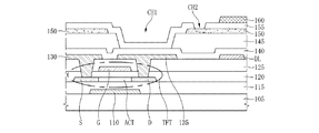
105 グラス基板
110 遮光層
115 バッファー層
120 ゲート絶縁層
125 層間絶縁層
130 ソースコンタクト部
135 ドレインコンタクト部
140 第1保護層
145 第2保護層
150 共通電極
155 第3保護層
160 伝導性ライン
170 画素電極
175 ブリッジコンタクト部
190 ドライブIC
TFT Thin Film Transistor
G ゲート電極
ACT アクティブ層
S ソース電極
D ドレイン電極
Claims (7)
- 複数の画素領域のそれぞれに配置されたTFT(Thin Film Transistor)と、
前記TFTのソース電極と接続されたソースコンタクト部及びドレイン電極と接続されたドレインコンタクト部と、
前記ソースコンタクト部及びドレインコンタクト部上に配置された第1保護層及び第2保護層と、
前記第2保護層上に配置された共通電極と、
前記共通電極上に配置された第3保護層と、
前記共通電極と重畳されるように前記第3保護層上に配置された伝導性ラインと、
第1コンタクトホールにおいて前記ドレインコンタクト部と接続され前記第3保護層上に配置された画素電極及び、
第1側が前記伝導性ラインと直接接続し、第2側が前記第3保護層を貫通して前記共通電極と接続されたブリッジコンタクト部と、を含むインセルタッチ液晶ディスプレイ装置。 - 前記共通電極を露出させる第2コンタクトホールに前記ブリッジコンタクト部が配置され、前記ブリッジコンタクト部と前記共通電極が接続された請求項1に記載のインセルタッチ液晶ディスプレイ装置。
- データラインと重畳された領域に、前記伝導性ラインと前記ブリッジコンタクト部の第1側が配置された請求項1に記載のインセルタッチ液晶ディスプレイ装置。
- 複数の画素領域のそれぞれにTFT(Thin Film Transistor)を形成する段階と、
前記TFTのソース電極と接続されるソースコンタクト部及びドレイン電極と接続されるドレインコンタクト部を形成する段階と、
前記ソースコンタクト部及びドレインコンタクト部上に第1保護層及び第2保護層を形成する段階と、
前記第2保護層上に共通電極を形成する段階と、
前記共通電極上に第3保護層を形成する段階と、
前記第3保護層上の前記共通電極と重畳された領域に伝導性ラインを形成する段階と、
前記ドレインコンタクト部を露出させる第1コンタクトホールを形成し、前記第1コンタクトホール内部及び前記第3保護層上に画素電極を形成する段階及び、
第1側が前記伝導性ラインと直接接続し、第2側が前記第3保護層を貫通して前記共通電極と接続されるブリッジコンタクト部を形成する段階と、を含むインセルタッチ液晶ディスプレイ装置の製造方法。 - 前記ドレインコンタクト部と重畳された領域の前記第1保護層乃至前記第3保護層を除去して前記第1コンタクトホールを形成し、
前記共通電極と重畳された領域の前記第3保護層を除去して第2コンタクトホールを形成する請求項4に記載のインセルタッチ液晶ディスプレイ装置の製造方法。 - 前記第2コンタクトホールに前記ブリッジコンタクト部の第2側が配置され、前記ブリッジコンタクト部と前記共通電極が接続される請求項5に記載のインセルタッチ液晶ディスプレイ装置の製造方法。
- 同一物質及び同一マスクを利用した製造工程で、前記画素電極と前記ブリッジコンタクト部を形成し、
前記ブリッジコンタクト部がアイランドパターンで形成されて前記画素電極と接続されない請求項4に記載のインセルタッチ液晶ディスプレイ装置の製造方法。
Applications Claiming Priority (2)
| Application Number | Priority Date | Filing Date | Title |
|---|---|---|---|
| KR1020140195970A KR101727108B1 (ko) | 2014-12-31 | 2014-12-31 | 인셀 터치 액정 디스플레이 장치와 이의 제조방법 |
| KR10-2014-0195970 | 2014-12-31 |
Publications (3)
| Publication Number | Publication Date |
|---|---|
| JP2016126336A JP2016126336A (ja) | 2016-07-11 |
| JP2016126336A5 JP2016126336A5 (ja) | 2016-09-15 |
| JP6018692B2 true JP6018692B2 (ja) | 2016-11-02 |
Family
ID=56163966
Family Applications (1)
| Application Number | Title | Priority Date | Filing Date |
|---|---|---|---|
| JP2015248466A Active JP6018692B2 (ja) | 2014-12-31 | 2015-12-21 | インセルタッチ液晶ディスプレイ装置及びその製造方法 |
Country Status (5)
| Country | Link |
|---|---|
| US (1) | US9454052B2 (ja) |
| JP (1) | JP6018692B2 (ja) |
| KR (1) | KR101727108B1 (ja) |
| CN (1) | CN105739739B (ja) |
| TW (1) | TWI571783B (ja) |
Families Citing this family (18)
| Publication number | Priority date | Publication date | Assignee | Title |
|---|---|---|---|---|
| US9910530B2 (en) * | 2015-02-27 | 2018-03-06 | Panasonic Liquid Crystal Display Co., Ltd. | Display panel with touch detection function |
| US20170017327A1 (en) * | 2015-07-17 | 2017-01-19 | Innolux Corporation | Touch display device |
| WO2018150988A1 (ja) * | 2017-02-15 | 2018-08-23 | シャープ株式会社 | 位置入力機能付き表示装置 |
| TWI691045B (zh) | 2017-02-20 | 2020-04-11 | 友達光電股份有限公司 | 電子組件、電子組件的製造方法及微元件的轉置方法 |
| JP6857563B2 (ja) | 2017-07-04 | 2021-04-14 | 株式会社ジャパンディスプレイ | 検出装置及び表示装置 |
| CN109407869B (zh) * | 2017-08-15 | 2021-11-09 | 京东方科技集团股份有限公司 | 触控结构及其制备方法、显示装置 |
| JP2019074684A (ja) | 2017-10-18 | 2019-05-16 | シャープ株式会社 | 表示パネル用基板の製造方法 |
| US10928691B2 (en) | 2019-02-15 | 2021-02-23 | Sharp Kabushiki Kaisha | Active matrix substrate comprising a first contact hole that overlaps with a counter electrode control line and passes through a flattening film and liquid crystal display with the same |
| CN110187800A (zh) * | 2019-05-17 | 2019-08-30 | 深圳市华星光电半导体显示技术有限公司 | 一种彩膜基板及其制备方法 |
| US11079636B2 (en) | 2019-10-25 | 2021-08-03 | Sharp Kabushiki Kaisha | Active matrix substrate, liquid crystal display device with touch sensor using active matrix substrate, and method for manufacturing active matrix substrate |
| US11243646B2 (en) | 2019-12-04 | 2022-02-08 | Sharp Kabushiki Kaisha | Display device |
| JP7299834B2 (ja) | 2019-12-26 | 2023-06-28 | シャープ株式会社 | アクティブマトリクス基板、アクティブマトリクス基板を備えたインセルタッチパネル型液晶表示装置、およびアクティブマトリクス基板の製造方法 |
| JP6800355B2 (ja) * | 2020-01-24 | 2020-12-16 | 株式会社ジャパンディスプレイ | 表示装置及びその製造方法 |
| US11637132B2 (en) | 2020-02-07 | 2023-04-25 | Sharp Kabushiki Kaisha | Active matrix substrate and method for manufacturing same |
| JP7383869B2 (ja) | 2020-02-13 | 2023-11-21 | シャープ株式会社 | タッチパネル及び表示装置 |
| US11557679B2 (en) | 2020-03-02 | 2023-01-17 | Sharp Kabushiki Kaisha | Active matrix substrate and display device |
| JP7463636B2 (ja) | 2020-08-17 | 2024-04-09 | シャープ株式会社 | タッチパネルおよび表示装置 |
| JP2022167632A (ja) | 2021-04-23 | 2022-11-04 | シャープディスプレイテクノロジー株式会社 | アクティブマトリクス基板、アクティブマトリクス基板の製造方法、およびアクティブマトリクス基板を用いたタッチセンサ付き液晶表示装置 |
Family Cites Families (24)
| Publication number | Priority date | Publication date | Assignee | Title |
|---|---|---|---|---|
| KR20050112878A (ko) * | 2004-05-28 | 2005-12-01 | 삼성전자주식회사 | 전기 영동 표시 장치 |
| KR20080052836A (ko) * | 2006-12-08 | 2008-06-12 | 삼성전자주식회사 | 액정 표시 장치 및 그 제조 방법 |
| KR101284714B1 (ko) * | 2010-09-20 | 2013-07-17 | 엘지디스플레이 주식회사 | 액정 표시장치와 이의 제조방법 |
| KR101320109B1 (ko) * | 2010-10-26 | 2013-10-18 | 엘지디스플레이 주식회사 | 평판 표시장치용 인-셀 터치 패널 |
| KR101295533B1 (ko) * | 2010-11-22 | 2013-08-12 | 엘지디스플레이 주식회사 | 액정표시장치 및 그 제조방법 |
| US9720295B2 (en) * | 2011-09-27 | 2017-08-01 | Lg Display Co., Ltd. | Liquid crystal display device and method for manufacturing the same |
| KR20130037072A (ko) * | 2011-10-05 | 2013-04-15 | 삼성전자주식회사 | 광터치 스크린 장치 및 그 제조 방법 |
| KR101524449B1 (ko) * | 2011-12-22 | 2015-06-02 | 엘지디스플레이 주식회사 | 액정표시장치 및 그 제조방법 |
| US9214501B2 (en) * | 2012-03-13 | 2015-12-15 | Mei, Inc. | In-cell OLED touch display panel structure |
| JP5922984B2 (ja) * | 2012-05-02 | 2016-05-24 | 株式会社ジャパンディスプレイ | 液晶表示装置 |
| KR101484022B1 (ko) * | 2012-05-31 | 2015-01-19 | 엘지디스플레이 주식회사 | 액정표시장치용 어레이 기판 및 이의 제조 방법 |
| KR101936773B1 (ko) | 2012-07-03 | 2019-01-09 | 엘지디스플레이 주식회사 | 액정 디스플레이 장치의 제조방법 |
| KR20140023492A (ko) * | 2012-08-16 | 2014-02-27 | 삼성코닝정밀소재 주식회사 | 스퍼터링 타겟 및 이에 의해 증착된 블랙 매트릭스를 포함하는 유기 발광 디스플레이 장치 |
| JP6022320B2 (ja) * | 2012-11-20 | 2016-11-09 | 株式会社ジャパンディスプレイ | 液晶表示装置 |
| TWI584028B (zh) * | 2012-12-28 | 2017-05-21 | 鴻海精密工業股份有限公司 | 液晶顯示面板及薄膜電晶體基板 |
| KR101690600B1 (ko) | 2012-12-28 | 2016-12-28 | 엘지디스플레이 주식회사 | 터치 스크린 일체형 표시장치 및 그 제조 방법 |
| US9213441B2 (en) * | 2013-09-06 | 2015-12-15 | Shenzhen China Star Optoelectronics Technology Co., Ltd. | In-cell touch panel and liquid crystal device |
| CN103699269B (zh) * | 2013-12-27 | 2017-02-01 | 京东方科技集团股份有限公司 | 一种双面触摸显示装置 |
| JP6400935B2 (ja) * | 2014-04-17 | 2018-10-03 | 株式会社ジャパンディスプレイ | 表示装置 |
| JP2015206829A (ja) * | 2014-04-17 | 2015-11-19 | 株式会社ジャパンディスプレイ | 表示装置 |
| US9753590B2 (en) * | 2014-06-13 | 2017-09-05 | Lg Display Co., Ltd. | Display device integrated with touch screen panel and method of fabricating the same |
| KR101655410B1 (ko) * | 2014-08-26 | 2016-09-07 | 엘지디스플레이 주식회사 | 인셀 터치 방식 액정표시장치 |
| TW201616323A (zh) * | 2014-10-17 | 2016-05-01 | 瑞鼎科技股份有限公司 | 內嵌式互電容觸控面板及其佈局 |
| KR102236460B1 (ko) * | 2014-10-31 | 2021-04-06 | 엘지디스플레이 주식회사 | 인셀 터치 액정 표시 장치와 이의 제조 방법, 박막트랜지스터 어레이 기판의 제조 방법 및 컬러필터 어레이 기판의 제조 방법 |
-
2014
- 2014-12-31 KR KR1020140195970A patent/KR101727108B1/ko active IP Right Grant
-
2015
- 2015-10-22 TW TW104134719A patent/TWI571783B/zh active
- 2015-11-05 US US14/933,498 patent/US9454052B2/en active Active
- 2015-11-19 CN CN201510800624.6A patent/CN105739739B/zh active Active
- 2015-12-21 JP JP2015248466A patent/JP6018692B2/ja active Active
Also Published As
| Publication number | Publication date |
|---|---|
| KR101727108B1 (ko) | 2017-04-17 |
| US9454052B2 (en) | 2016-09-27 |
| CN105739739A (zh) | 2016-07-06 |
| CN105739739B (zh) | 2018-01-23 |
| JP2016126336A (ja) | 2016-07-11 |
| US20160187690A1 (en) | 2016-06-30 |
| TWI571783B (zh) | 2017-02-21 |
| KR20160083626A (ko) | 2016-07-12 |
| TW201626191A (zh) | 2016-07-16 |
Similar Documents
| Publication | Publication Date | Title |
|---|---|---|
| JP6018692B2 (ja) | インセルタッチ液晶ディスプレイ装置及びその製造方法 | |
| JP6417311B2 (ja) | インセルタッチ液晶ディスプレイ装置及びその製造方法 | |
| US9971181B2 (en) | In-cell touch liquid crystal display device and method for manufacturing the same | |
| US10310345B2 (en) | In-cell touch liquid crystal display apparatus, method of manufacturing the same, method of manufacturing thin film transistor array substrate, and method of manufacturing color filter array substrate | |
| US9470923B2 (en) | In-cell touch liquid crystal display device and method of manufacturing the same | |
| US10151947B2 (en) | In-cell touch liquid crystal display device and method of manufacturing the same | |
| US8743301B2 (en) | Liquid crystal display device provided with an electrode for sensing a touch of a user | |
| CN102566171B (zh) | 液晶显示设备和制造该液晶显示设备的方法 | |
| KR101749146B1 (ko) | 터치 스크린이 내장된 액정 표시장치와 이의 제조방법 | |
| KR101608637B1 (ko) | 터치 스크린이 내장된 액정 표시장치와 이의 제조방법 | |
| CN102411237A (zh) | 液晶显示装置及其制造方法 |
Legal Events
| Date | Code | Title | Description |
|---|---|---|---|
| A521 | Request for written amendment filed |
Free format text: JAPANESE INTERMEDIATE CODE: A523 Effective date: 20160725 |
|
| A871 | Explanation of circumstances concerning accelerated examination |
Free format text: JAPANESE INTERMEDIATE CODE: A871 Effective date: 20160725 |
|
| A975 | Report on accelerated examination |
Free format text: JAPANESE INTERMEDIATE CODE: A971005 Effective date: 20160822 |
|
| TRDD | Decision of grant or rejection written | ||
| A01 | Written decision to grant a patent or to grant a registration (utility model) |
Free format text: JAPANESE INTERMEDIATE CODE: A01 Effective date: 20160906 |
|
| A61 | First payment of annual fees (during grant procedure) |
Free format text: JAPANESE INTERMEDIATE CODE: A61 Effective date: 20160930 |
|
| R150 | Certificate of patent or registration of utility model |
Ref document number: 6018692 Country of ref document: JP Free format text: JAPANESE INTERMEDIATE CODE: R150 |
|
| R250 | Receipt of annual fees |
Free format text: JAPANESE INTERMEDIATE CODE: R250 |
|
| R250 | Receipt of annual fees |
Free format text: JAPANESE INTERMEDIATE CODE: R250 |
|
| R250 | Receipt of annual fees |
Free format text: JAPANESE INTERMEDIATE CODE: R250 |
|
| R250 | Receipt of annual fees |
Free format text: JAPANESE INTERMEDIATE CODE: R250 |
|
| R250 | Receipt of annual fees |
Free format text: JAPANESE INTERMEDIATE CODE: R250 |