JP6012689B2 - Electrochromic element, optical filter, lens unit, imaging device - Google Patents
Electrochromic element, optical filter, lens unit, imaging device Download PDFInfo
- Publication number
- JP6012689B2 JP6012689B2 JP2014219767A JP2014219767A JP6012689B2 JP 6012689 B2 JP6012689 B2 JP 6012689B2 JP 2014219767 A JP2014219767 A JP 2014219767A JP 2014219767 A JP2014219767 A JP 2014219767A JP 6012689 B2 JP6012689 B2 JP 6012689B2
- Authority
- JP
- Japan
- Prior art keywords
- electrochromic
- max
- molecules
- types
- molecule
- Prior art date
- Legal status (The legal status is an assumption and is not a legal conclusion. Google has not performed a legal analysis and makes no representation as to the accuracy of the status listed.)
- Active
Links
Images


Classifications
-
- G—PHYSICS
- G02—OPTICS
- G02F—OPTICAL DEVICES OR ARRANGEMENTS FOR THE CONTROL OF LIGHT BY MODIFICATION OF THE OPTICAL PROPERTIES OF THE MEDIA OF THE ELEMENTS INVOLVED THEREIN; NON-LINEAR OPTICS; FREQUENCY-CHANGING OF LIGHT; OPTICAL LOGIC ELEMENTS; OPTICAL ANALOGUE/DIGITAL CONVERTERS
- G02F1/00—Devices or arrangements for the control of the intensity, colour, phase, polarisation or direction of light arriving from an independent light source, e.g. switching, gating or modulating; Non-linear optics
- G02F1/01—Devices or arrangements for the control of the intensity, colour, phase, polarisation or direction of light arriving from an independent light source, e.g. switching, gating or modulating; Non-linear optics for the control of the intensity, phase, polarisation or colour
- G02F1/15—Devices or arrangements for the control of the intensity, colour, phase, polarisation or direction of light arriving from an independent light source, e.g. switching, gating or modulating; Non-linear optics for the control of the intensity, phase, polarisation or colour based on an electrochromic effect
- G02F1/1503—Devices or arrangements for the control of the intensity, colour, phase, polarisation or direction of light arriving from an independent light source, e.g. switching, gating or modulating; Non-linear optics for the control of the intensity, phase, polarisation or colour based on an electrochromic effect caused by oxidation-reduction reactions in organic liquid solutions, e.g. viologen solutions
-
- G—PHYSICS
- G02—OPTICS
- G02F—OPTICAL DEVICES OR ARRANGEMENTS FOR THE CONTROL OF LIGHT BY MODIFICATION OF THE OPTICAL PROPERTIES OF THE MEDIA OF THE ELEMENTS INVOLVED THEREIN; NON-LINEAR OPTICS; FREQUENCY-CHANGING OF LIGHT; OPTICAL LOGIC ELEMENTS; OPTICAL ANALOGUE/DIGITAL CONVERTERS
- G02F1/00—Devices or arrangements for the control of the intensity, colour, phase, polarisation or direction of light arriving from an independent light source, e.g. switching, gating or modulating; Non-linear optics
- G02F1/01—Devices or arrangements for the control of the intensity, colour, phase, polarisation or direction of light arriving from an independent light source, e.g. switching, gating or modulating; Non-linear optics for the control of the intensity, phase, polarisation or colour
- G02F1/15—Devices or arrangements for the control of the intensity, colour, phase, polarisation or direction of light arriving from an independent light source, e.g. switching, gating or modulating; Non-linear optics for the control of the intensity, phase, polarisation or colour based on an electrochromic effect
- G02F1/163—Operation of electrochromic cells, e.g. electrodeposition cells; Circuit arrangements therefor
-
- G—PHYSICS
- G09—EDUCATION; CRYPTOGRAPHY; DISPLAY; ADVERTISING; SEALS
- G09G—ARRANGEMENTS OR CIRCUITS FOR CONTROL OF INDICATING DEVICES USING STATIC MEANS TO PRESENT VARIABLE INFORMATION
- G09G3/00—Control arrangements or circuits, of interest only in connection with visual indicators other than cathode-ray tubes
- G09G3/20—Control arrangements or circuits, of interest only in connection with visual indicators other than cathode-ray tubes for presentation of an assembly of a number of characters, e.g. a page, by composing the assembly by combination of individual elements arranged in a matrix no fixed position being assigned to or needed to be assigned to the individual characters or partial characters
- G09G3/34—Control arrangements or circuits, of interest only in connection with visual indicators other than cathode-ray tubes for presentation of an assembly of a number of characters, e.g. a page, by composing the assembly by combination of individual elements arranged in a matrix no fixed position being assigned to or needed to be assigned to the individual characters or partial characters by control of light from an independent source
- G09G3/38—Control arrangements or circuits, of interest only in connection with visual indicators other than cathode-ray tubes for presentation of an assembly of a number of characters, e.g. a page, by composing the assembly by combination of individual elements arranged in a matrix no fixed position being assigned to or needed to be assigned to the individual characters or partial characters by control of light from an independent source using electrochromic devices
-
- H—ELECTRICITY
- H04—ELECTRIC COMMUNICATION TECHNIQUE
- H04N—PICTORIAL COMMUNICATION, e.g. TELEVISION
- H04N23/00—Cameras or camera modules comprising electronic image sensors; Control thereof
- H04N23/70—Circuitry for compensating brightness variation in the scene
- H04N23/75—Circuitry for compensating brightness variation in the scene by influencing optical camera components
-
- G—PHYSICS
- G02—OPTICS
- G02F—OPTICAL DEVICES OR ARRANGEMENTS FOR THE CONTROL OF LIGHT BY MODIFICATION OF THE OPTICAL PROPERTIES OF THE MEDIA OF THE ELEMENTS INVOLVED THEREIN; NON-LINEAR OPTICS; FREQUENCY-CHANGING OF LIGHT; OPTICAL LOGIC ELEMENTS; OPTICAL ANALOGUE/DIGITAL CONVERTERS
- G02F1/00—Devices or arrangements for the control of the intensity, colour, phase, polarisation or direction of light arriving from an independent light source, e.g. switching, gating or modulating; Non-linear optics
- G02F1/01—Devices or arrangements for the control of the intensity, colour, phase, polarisation or direction of light arriving from an independent light source, e.g. switching, gating or modulating; Non-linear optics for the control of the intensity, phase, polarisation or colour
- G02F1/15—Devices or arrangements for the control of the intensity, colour, phase, polarisation or direction of light arriving from an independent light source, e.g. switching, gating or modulating; Non-linear optics for the control of the intensity, phase, polarisation or colour based on an electrochromic effect
- G02F1/1514—Devices or arrangements for the control of the intensity, colour, phase, polarisation or direction of light arriving from an independent light source, e.g. switching, gating or modulating; Non-linear optics for the control of the intensity, phase, polarisation or colour based on an electrochromic effect characterised by the electrochromic material, e.g. by the electrodeposited material
- G02F1/1516—Devices or arrangements for the control of the intensity, colour, phase, polarisation or direction of light arriving from an independent light source, e.g. switching, gating or modulating; Non-linear optics for the control of the intensity, phase, polarisation or colour based on an electrochromic effect characterised by the electrochromic material, e.g. by the electrodeposited material comprising organic material
- G02F1/15165—Polymers
-
- G—PHYSICS
- G02—OPTICS
- G02F—OPTICAL DEVICES OR ARRANGEMENTS FOR THE CONTROL OF LIGHT BY MODIFICATION OF THE OPTICAL PROPERTIES OF THE MEDIA OF THE ELEMENTS INVOLVED THEREIN; NON-LINEAR OPTICS; FREQUENCY-CHANGING OF LIGHT; OPTICAL LOGIC ELEMENTS; OPTICAL ANALOGUE/DIGITAL CONVERTERS
- G02F1/00—Devices or arrangements for the control of the intensity, colour, phase, polarisation or direction of light arriving from an independent light source, e.g. switching, gating or modulating; Non-linear optics
- G02F1/01—Devices or arrangements for the control of the intensity, colour, phase, polarisation or direction of light arriving from an independent light source, e.g. switching, gating or modulating; Non-linear optics for the control of the intensity, phase, polarisation or colour
- G02F1/15—Devices or arrangements for the control of the intensity, colour, phase, polarisation or direction of light arriving from an independent light source, e.g. switching, gating or modulating; Non-linear optics for the control of the intensity, phase, polarisation or colour based on an electrochromic effect
- G02F1/153—Constructional details
- G02F1/157—Structural association of cells with optical devices, e.g. reflectors or illuminating devices
-
- G—PHYSICS
- G02—OPTICS
- G02F—OPTICAL DEVICES OR ARRANGEMENTS FOR THE CONTROL OF LIGHT BY MODIFICATION OF THE OPTICAL PROPERTIES OF THE MEDIA OF THE ELEMENTS INVOLVED THEREIN; NON-LINEAR OPTICS; FREQUENCY-CHANGING OF LIGHT; OPTICAL LOGIC ELEMENTS; OPTICAL ANALOGUE/DIGITAL CONVERTERS
- G02F1/00—Devices or arrangements for the control of the intensity, colour, phase, polarisation or direction of light arriving from an independent light source, e.g. switching, gating or modulating; Non-linear optics
- G02F1/01—Devices or arrangements for the control of the intensity, colour, phase, polarisation or direction of light arriving from an independent light source, e.g. switching, gating or modulating; Non-linear optics for the control of the intensity, phase, polarisation or colour
- G02F1/15—Devices or arrangements for the control of the intensity, colour, phase, polarisation or direction of light arriving from an independent light source, e.g. switching, gating or modulating; Non-linear optics for the control of the intensity, phase, polarisation or colour based on an electrochromic effect
- G02F1/163—Operation of electrochromic cells, e.g. electrodeposition cells; Circuit arrangements therefor
- G02F2001/1635—Operation of electrochromic cells, e.g. electrodeposition cells; Circuit arrangements therefor the pixel comprises active switching elements, e.g. TFT
Landscapes
- Physics & Mathematics (AREA)
- Nonlinear Science (AREA)
- General Physics & Mathematics (AREA)
- Engineering & Computer Science (AREA)
- Optics & Photonics (AREA)
- Chemical & Material Sciences (AREA)
- Chemical Kinetics & Catalysis (AREA)
- Signal Processing (AREA)
- Multimedia (AREA)
- Computer Hardware Design (AREA)
- Theoretical Computer Science (AREA)
- Electrochromic Elements, Electrophoresis, Or Variable Reflection Or Absorption Elements (AREA)
- Optical Elements Other Than Lenses (AREA)
Description
本発明は、エレクトロクロミック素子、光学フィルタ、レンズユニット、撮像装置に関する。 The present invention relates to an electrochromic element, an optical filter, a lens unit, and an imaging device.
電気化学的な酸化還元反応により、物質の光学吸収の性質(吸収波長、吸光度)が変化するエレクトロクロミック材料を利用したエレクトロクロミック素子は、表示装置、可変反射率ミラー、透過率可変窓等に応用されている。 Electrochromic devices using electrochromic materials whose optical absorption properties (absorption wavelength, absorbance) change due to electrochemical redox reactions can be applied to display devices, variable reflectance mirrors, variable transmittance windows, etc. Has been.
このようなエレクトロクロミック素子のうちの有機エレクトロクロミック素子として、特許文献1には、吸収波長の異なる複数の有機低分子エレクトロクロミック分子が溶媒に溶解した溶液を有機エレクトロクロミック層として有する有機エレクトロクロミック素子が記載されている。
As an organic electrochromic element among such electrochromic elements,
しかしながら、特許文献1に記載の有機エレクトロクロミック素子では、有機エレクトロクロミック層のエレクトロクロミック分子の拡散係数の違いにより、着色動作時の色バランスが変化する領域があると考えられる。
However, in the organic electrochromic element described in
このような色バランスの変化は、有機エレクトロクロミック素子を、例えば、撮像装置における光量調整手段(たとえばNDフィルタ)や表示装置のカラーフィルタなどとして利用する場合などにおいて好ましくないため、低減する必要がある。 Such a change in color balance is not preferable when the organic electrochromic element is used as, for example, a light amount adjusting means (for example, an ND filter) in an imaging apparatus or a color filter in a display apparatus, and thus needs to be reduced. .
そこで、本発明では、一対の電極と、前記一対の電極の間に配置され、複数種類の同極性のエレクトロクロミック分子を有するエレクトロクロミック層と、を有し、前記複数種類の同極性のエレクトロクロミック分子から前記エレクトロクロミック層の着色時の最大吸光度が大きい順に2種類の分子を選択した場合に、前記2種類の分子各々の前記エレクトロクロミック層の着色時における拡散係数のうち、小さい方の拡散係数D2min、大きい方の拡散係数D2max、及び前記2種類の分子のうち拡散係数が前記D2maxである分子の前記エレクトロクロミック層の着色時の最大吸光度H2が、下記式(5)を満たすことを特徴とするエレクトロクロミック素子を提供する。
1≦D2max/D2min≦(1+0.146/H2)2 (5)
Therefore, in the present invention, a pair of electrodes, disposed between the pair of electrodes has a electrochromic layer having the electrochromic molecules of a plurality of types of the same polarity, the previous SL plurality of types of the same polarity of electro when the chromic molecules were selected two molecules in order maximum absorbance is large at the time of coloring the electrochromic layer, of the diffusion coefficient at the time of coloring before Symbol electrochromic layer of the two kinds of molecules each smaller Diffusion coefficient D 2 min, the larger diffusion coefficient D 2 max, and the maximum absorbance H 2 when coloring the electrochromic layer of the molecule of which the diffusion coefficient is D 2 max among the two types of molecules is expressed by the following formula: An electrochromic element characterized by satisfying (5) is provided.
1 ≦ D 2 max / D 2 min ≦ (1 + 0.146 / H 2 ) 2 (5)
また、別の本発明では、一対の電極と、前記一対の電極の間に配置され、複数種類の同極性のエレクトロクロミック分子を有するエレクトロクロミック層と、有し、前記複数種類の同極性のエレクトロクロミック分子として3種類以上の同極性のエレクトロクロミック分子を前記エレクトロクロミック層に有し、前記複数種類の同極性のエレクトロクロミック分子から前記エレクトロクロミック層の着色時の最大吸光度が大きい順に3種類の分子を選択した場合に、前記3種類の分子各々の前記エレクトロクロミック層の着色時における拡散係数のうち、最も小さな拡散係数D 3 min、最も大きな拡散係数をD 3 max、及び前記3種類の分子のうち拡散係数が前記D3maxである分子の前記エレクトロクロミック層の着色時の最大吸光度H3が、下記式(5a)を満たすことを特徴とするエレクトロクロミック素子を提供する。
1≦D3max/D3min≦(1+0.146/H3)2 (5a)
さらに、別の本発明では、一対の電極と、前記一対の電極の間に配置され、複数種類の同極性のエレクトロクロミック分子を有するエレクトロクロミック層と、を有し、前記複数種類の同極性のエレクトロクロミック分子から前記エレクトロクロミック層の着色時の最大吸光度が最も大きい分子と該最大吸光度が最も大きい分子の最大吸光度の1/10以上の最大吸光度を有する分子群のうちの任意の一つの分子との各々の拡散係数のうち、小さい方の拡散係数DNmin、大きい方の拡散係数DNmax、及び前記分子のうち拡散係数が前記DNmaxである分子の前記エレクトロクロミック層の着色時の最大吸光度HNが、下記式(5b)を満たすことを特徴とするエレクトロクロミック素子を提供する。
1≦DNmax/DNmin≦(1+0.146/HN)2 (5b)
In another aspect of the present invention, the electrochromic layer includes a pair of electrodes and an electrochromic layer disposed between the pair of electrodes and having a plurality of types of electrochromic molecules having the same polarity. Three or more types of electrochromic molecules having the same polarity as the chromic molecule in the electrochromic layer, and the three types of molecules in descending order of the maximum absorbance when coloring the electrochromic layer from the plurality of types of electrochromic molecules having the same polarity Of the three types of molecules when coloring the electrochromic layer, the smallest diffusion coefficient D 3 min, the largest diffusion coefficient D 3 max, and the three types of molecules maximum out diffusion coefficient at the time of coloring the electrochromic layer of the molecule which is the D 3 max Luminous intensity H 3, provides an electrochromic device characterized by satisfying the following formula (5a).
1 ≦ D 3 max / D 3 min ≦ (1 + 0.146 / H 3 ) 2 (5a)
Further, in another aspect of the present invention, the electrochromic layer has a pair of electrodes and an electrochromic layer disposed between the pair of electrodes and having a plurality of types of electrochromic molecules, and the plurality of types of the same polarity. A molecule having the largest maximum absorbance when coloring the electrochromic layer from an electrochromic molecule, and any one molecule in a group of molecules having a maximum absorbance of 1/10 or more of the maximum absorbance of the molecule having the largest maximum absorbance; Among the respective diffusion coefficients, a smaller diffusion coefficient D N min, a larger diffusion coefficient D N max, and a molecule having a diffusion coefficient of D N max among the molecules at the time of coloring the electrochromic layer maximum absorbance H N, provides an electrochromic device characterized by satisfying the following formula (5b).
1 ≦ D N max / D N min ≦ (1 + 0.146 / H N ) 2 (5b)
本発明によれば、着色動作時の有機エレクトロクロミック素子の色バランス変化を抑制した有機エレクトロクロミック素子を提供することができる。 ADVANTAGE OF THE INVENTION According to this invention, the organic electrochromic element which suppressed the color balance change of the organic electrochromic element at the time of coloring operation can be provided.
はじめに、本実施形態の有機エレクトロクロミック素子の前提となる物質輸送の拡散プロセスについて説明する。なお、以下、「エレクトロクロミック」を「EC」と略記する場合がある。 First, a diffusion process of material transport, which is a premise of the organic electrochromic device of this embodiment, will be described. Hereinafter, “electrochromic” may be abbreviated as “EC”.
溶媒とそれに溶解したエレクトロクロミック分子を有する溶液がエレクトロクロミック層である「タイプI」と呼ばれる形式のエレクトロクロミック素子の着色時には、電極間に、分子が着色する酸化反応、もしくは還元反応を進行させるのに十分な電位差を与える。その際、着色プロセスは、未着色のエレクトロクロミック分子が電極に移動する物質輸送が律速となるプロセスとなる。一般に攪拌等の外部要因のない溶液中における電極への物質輸送によって与えられる電解電流は、下に示すコットレルの式で記述される。 When coloring an electrochromic device of the type called “type I” in which a solution having a solvent and an electrochromic molecule dissolved in the solvent is an electrochromic layer, an oxidation reaction or a reduction reaction in which a molecule is colored proceeds between electrodes. Give a sufficient potential difference. In this case, the coloring process is a process in which the material transport in which the uncolored electrochromic molecules move to the electrode is rate-determined. In general, the electrolytic current given by the material transport to the electrode in a solution free from external factors such as stirring is described by the Cottrell equation shown below.

ここで、i(t):電解電流、n:一分子反応時にかかわる電子数、F:ファラデー定数、c:EC分子のバルク濃度(すなわち、溶液の初期濃度)、A:電極面積、D:拡散係数、t:時間 Here, i (t): electrolytic current, n: number of electrons involved in a single molecule reaction, F: Faraday constant, c: bulk concentration of EC molecule (ie, initial concentration of solution), A: electrode area, D: diffusion Coefficient, t: time
これを時間積分した電荷量Q(t)は、以下の式で与えられる。 The charge amount Q (t) obtained by integrating this over time is given by the following equation.
ここで、溶液中に複数種類のエレクトロクロミック材料n、mを混合した場合においてはこれらの材料間の吸光度の比(Absn(t)/Absm(t))は、以下の式で与えられる。 Here, when a plurality of types of electrochromic materials n and m are mixed in the solution, the ratio of absorbance between these materials (Abs n (t) / Abs m (t)) is given by the following equation. .
(ここで、ε:エレクトロクロミック分子の着色体のモル吸光係数、l:光路長) (Where ε: molar extinction coefficient of colored body of electrochromic molecule, l: optical path length)
ここから、吸光度の比は、時間によって変化することはないことがわかる。そして、分子間の拡散係数、モル吸光係数の違いは、バルク濃度で補償することが可能であることがわかる。 From this, it can be seen that the absorbance ratio does not change with time. And it turns out that the difference in the diffusion coefficient between molecules and the molar extinction coefficient can be compensated by the bulk concentration.
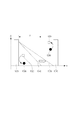
図1に、薄層のエレクトロクロミック層を有する有機エレクトロクロミック素子の着色メカニズムを示す。図中縦軸(c)は、着色したエレクトロクロミック分子の濃度、横軸(x)は、着色反応に必要な電位が印加される電極からの距離を示す。1000は、エレクトロクロミック分子が着色する反応がおこなわれる電極であり、1010はその対向電極である。 FIG. 1 shows a coloring mechanism of an organic electrochromic device having a thin electrochromic layer. In the figure, the vertical axis (c) indicates the concentration of colored electrochromic molecules, and the horizontal axis (x) indicates the distance from the electrode to which a potential necessary for the coloring reaction is applied. 1000 is an electrode in which a reaction for coloring the electrochromic molecule is performed, and 1010 is the counter electrode.
図1において、未着色のエレクトロクロミック分子1020は、着色反応に必要な電位が電極1000に印加されると、着色したエレクトロクロミック分子1030となる。これにより、有機エレクトロクロミック層には、1040で表されるような着色したエレクトロクロミック分子の濃度プロファイルが形成される。この濃度プロファイルが形成される領域においては、エレクトロクロミック素子における複数のエレクトロクロミック材料が一定比率で着色するというメカニズムは有効に機能し、エレクトロクロミック素子の色バランスは、時間に対して変動しないと考えられる。
In FIG. 1, uncolored
しかしながら、薄層のエレクトロクロミック層において、Xで示す着色したエレクトロクロミック分子の拡散層が対向電極に達し、1050のような濃度プロファイルとなった場合には、対向電極は、1000の電極と逆の反応が進行する電位となっているため、着色したエレクトロクロミック分子1060から未着色のエレクトロクロミック分子1070への反応がおこなわれる。そのため、その時点以降ではセル全体の着色体の濃度は変化しない、または、変化するとしてもその濃度の増大の程度は小さくなる。
However, in the thin electrochromic layer, when the colored electrochromic molecular diffusion layer indicated by X reaches the counter electrode and has a concentration profile such as 1050, the counter electrode is the opposite of 1000 electrodes. Since the potential is such that the reaction proceeds, the reaction from the colored
エレクトロクロミック層における同極性の複数種類のエレクトロクロミック分子(アノード性の複数種類のエレクトロクロミック分子、またはカソード性の複数種類のエレクトロクロミック分子)を共存させた場合には、それぞれのエレクトロクロミック分子の着色体の拡散層が対向電極へ到達するタイミングが異なる。 When multiple types of electrochromic molecules of the same polarity in the electrochromic layer (multiple types of anodic electrochromic molecules or multiple types of cathodic electrochromic molecules) coexist, coloring of each electrochromic molecule The timing at which the body diffusion layer reaches the counter electrode is different.
電気化学反応における拡散層の厚み(δ(t))は、下式(4)で表されるように、拡散係数と時間の積の平方根に比例することが予想される。 The thickness (δ (t)) of the diffusion layer in the electrochemical reaction is expected to be proportional to the square root of the product of the diffusion coefficient and time, as represented by the following equation (4).
![]()
![]()
したがって、有機エレクトロクロミック層に複数種類の同極性のエレクトロクロミック材料が存在すると、式(4)に示したように、着色体(着色したエレクトロクロミック材料)の拡散層が対向電極へ到達する時間が異なり、その結果として色バランスの変化が生じる。 Therefore, when a plurality of types of electrochromic materials having the same polarity exist in the organic electrochromic layer, as shown in the formula (4), the time for the diffusion layer of the colored body (colored electrochromic material) to reach the counter electrode Differently, the result is a change in color balance.
この前提に基づき、本実施形態のエレクトロクロミック素子について以下に記載する。 Based on this premise, the electrochromic device of this embodiment will be described below.
(第1の実施形態)
本実施形態のエレクトロクロミック素子は、一対の電極と、前記一対の電極の間に配置されているエレクトロクロミック層と、を有するエレクトロクロミック素子であって、
前記エレクトロクロミック層は、複数種類の同極性のエレクトロクロミック分子を有し、
前記エレクトロクロミック層の着色時に前記複数種類の同極性のエレクトロクロミック分子のうち最大吸光度が大きい順に2種類の分子を選択した時に、前記2種類の分子各々の、前記エレクトロクロミック層の着色時における拡散係数のうち、小さい方の拡散係数D2min、大きい方の拡散係数D2max、前記2種類の分子のうち拡散係数が前記D2maxである分子の前記エレクトロクロミック層の着色時の最大吸光度H2が、下記式(5)を満たすエレクトロクロミック素子である。
1≦D2max/D2min≦(1+0.146/H2)2 (5)
(First embodiment)
The electrochromic device of the present embodiment is an electrochromic device having a pair of electrodes and an electrochromic layer disposed between the pair of electrodes,
The electrochromic layer has a plurality of types of electrochromic molecules of the same polarity,
When two types of molecules are selected in descending order of maximum absorbance among the plurality of types of electrochromic molecules of the same polarity when coloring the electrochromic layer, diffusion of the two types of molecules during coloring of the electrochromic layer Among the coefficients, the smaller diffusion coefficient D 2 min, the larger diffusion coefficient D 2 max, and the maximum absorbance at the time of coloring of the electrochromic layer of the molecules having the diffusion coefficient D 2 max among the two kinds of molecules H 2 is an electrochromic element that satisfies the following formula (5).
1 ≦ D 2 max / D 2 min ≦ (1 + 0.146 / H 2 ) 2 (5)
図2に、本実施形態の有機エレクトロクロミック素子の断面の模式図を示す。 In FIG. 2, the schematic diagram of the cross section of the organic electrochromic element of this embodiment is shown.
図2において、2000および2010は電極であり、2020は、それらの電極間に存在する有機エレクトロクロミック層である。有機エレクトロクロミック層2020は、シール材2030によって外部と隔離されて保持されている。
In FIG. 2, 2000 and 2010 are electrodes, and 2020 is an organic electrochromic layer existing between the electrodes. The organic
以下に、本実施形態の有機エレクトロクロミック素子が有する構成要素について、以下に項目に分けて説明を記載する。 Below, the component which the organic electrochromic element of this embodiment has is divided into items and described below.
(1)電極
本実施形態の有機エレクトロクロミック素子が有する一対の電極(2000、2010)のうちの一方の電極は、透明電極であることが好ましい。
(1) Electrode It is preferable that one electrode of a pair of electrodes (2000, 2010) which the organic electrochromic element of this embodiment has is a transparent electrode.
ここで、透明とは、光を透過することを意味し、光の透過率が、50%以上100%以下であることが好ましい。これは、少なくとも一方の電極が透明電極であることによって、有機エレクトロクロミック素子の外部より効率的に光を取り込み、エレクトロクロミック分子と相互作用させて、エレクトロクロミック分子の光学的特性を出射光に反映させることができるからである。また、ここにおいて、透過する光とは、エレクトロクロミック素子の対象とする波長領域における光のことである。例えば、エレクトロクロミック素子を可視光領域の撮像装置のフィルタとして使用するのであれば、可視光領域の光、赤外線領域の撮像装置のフィルタとして使用するのであれば、赤外線領域の光である。 Here, the term “transparent” means that light is transmitted, and the light transmittance is preferably 50% or more and 100% or less. This is because when at least one of the electrodes is a transparent electrode, light is efficiently captured from the outside of the organic electrochromic device and interacts with the electrochromic molecule to reflect the optical characteristics of the electrochromic molecule in the emitted light. It is because it can be made. In addition, here, the transmitted light is light in a wavelength region targeted by the electrochromic element. For example, if an electrochromic element is used as a filter for an imaging device in the visible light region, light in the visible light region is used, and if used as a filter for an imaging device in the infrared region, the light is in the infrared region.
このような透明電極としては、ガラスもしくは高分子化合物の基板に透明導電性酸化物の層が形成された透明導電性酸化物電極が好ましい。透明導電性酸化物の例としては、スズドープ酸化インジウム(ITO)、酸化亜鉛、ガリウムドープ酸化亜鉛(GZO)、アルミニウムドープ酸化亜鉛(AZO)、酸化スズ、アンチモンドープ酸化スズ(ATO)、フッ素ドープ酸化スズ(FTO)、ニオビウムドープ酸化チタン(TNO)が挙げられる。これらのうちでも、透明導電性酸化物の層は、膜厚10nm〜10000nmのFTOまたはITOの層であることが好ましい。これにより、高透過性と化学的安定性を両立することが可能となるからである。 As such a transparent electrode, a transparent conductive oxide electrode in which a transparent conductive oxide layer is formed on a glass or polymer compound substrate is preferable. Examples of transparent conductive oxides include tin-doped indium oxide (ITO), zinc oxide, gallium-doped zinc oxide (GZO), aluminum-doped zinc oxide (AZO), tin oxide, antimony-doped tin oxide (ATO), and fluorine-doped oxidation. Examples thereof include tin (FTO) and niobium-doped titanium oxide (TNO). Among these, the transparent conductive oxide layer is preferably an FTO or ITO layer having a thickness of 10 nm to 10000 nm. This is because it is possible to achieve both high permeability and chemical stability.
なお、透明導電性酸化物の層は、透明導電性酸化物のサブレイヤーが積み重なった構成をなしていても良い。これにより、高導電性と高透明性を実現しやすくなる。 The transparent conductive oxide layer may have a structure in which transparent conductive oxide sublayers are stacked. Thereby, it becomes easy to realize high conductivity and high transparency.
一対の電極のうちの他方の電極は、EC素子の用途に応じて好ましいものが選択される。例えば、本実施形態の有機エレクトロクロミック素子を透過型エレクトロミック素子とする場合には、他方の電極も透明電極であることが好ましく、よりこのましくは前述した透明導電性酸化物電極である。 As the other electrode of the pair of electrodes, a preferable electrode is selected according to the use of the EC element. For example, when the organic electrochromic element of this embodiment is a transmissive electromic element, the other electrode is also preferably a transparent electrode, more preferably the above-described transparent conductive oxide electrode.
一方、本実施形態の有機エレクトロクロミック素子を反射型エレクトロミック素子とする場合には、他方の電極には、入射光を反射する電極を用いることが好ましい。 On the other hand, when the organic electrochromic element of the present embodiment is a reflective electromic element, it is preferable to use an electrode that reflects incident light as the other electrode.
本実施形態の有機エレクトロクロミック素子が、いずれの形態の素子であっても、一対の電極の材料には、有機エレクトロクロミック素子の動作環境において安定に存在し、外部からの電圧の印加に応じて速やかに酸化還元反応を進行させることのできる材料が好ましく用いられる。 Even if the organic electrochromic element of this embodiment is an element of any form, the material of the pair of electrodes is stably present in the operating environment of the organic electrochromic element, and according to the application of an external voltage. A material capable of promptly proceeding the oxidation-reduction reaction is preferably used.
なお、本実施形態の有機エレクトロクロミック素子は、必要に応じて、これら一対の電極以外の電極を有していても良い。例えば、有機エレクトロクロミック層の電位についての情報を得るために、参照電極を有していても良い。また、例えば、分割着色の目的等で、一対の電極のうちの一方または両方を複数の電極から構成してもよい。 In addition, the organic electrochromic element of this embodiment may have electrodes other than these pair of electrodes as needed. For example, in order to obtain information on the potential of the organic electrochromic layer, a reference electrode may be provided. Further, for example, one or both of the pair of electrodes may be composed of a plurality of electrodes for the purpose of division coloring.
一対の電極(2000、2010)は、電極面を対向させた配置でシール材2030によって接合されている。
A pair of electrodes (2000, 2010) are joined by a
シール材2030としては、化学的に安定で、気体および液体を透過せず、エレクトロクロミック材料の酸化還元反応を阻害しない材料であることが好ましく、例えばガラスフリット等の無機材料、エポキシ樹脂等の有機材料、金属等を用いることができる。なお、シール材2030は、一対の電極の電極間距離を保持する機能を有していても良い。シール材2030が一対の電極の電極間距離を規定する機能を有していない場合には、別途スペーサーを配置して一対の電極の電極間距離を保持しても良い。このような場合のスペーサーの素材としては、シリカビーズ、ガラスファイバー、のような無機材料や、ポリイミド、ポリテトラフルオロエチレン、フッ素ゴム、エポキシ樹脂等の有機材料を用いることができる。このスペーサーにより、EC素子の電極間距離を規定、保持することが可能である。
The
一対の電極の電極間距離は、0.6μm以上130μm以下であることが好ましい。電極間距離が0.6μm以上であることにより、有機エレクトロミック素子として有効に機能させるために十分な量のエレクトロクロミック材料を配置することができる空間となる。また、電極間距離が130μm以下であることにより、速い応答速度を達成することができる。これは、130μm以下であることにより、自然対流による物質輸送に対して拡散による物質輸送の影響が大きくすることができるからである。 The distance between the pair of electrodes is preferably 0.6 μm or more and 130 μm or less. When the distance between the electrodes is 0.6 μm or more, a space in which a sufficient amount of electrochromic material can be disposed to effectively function as an organic electromic element is provided. Further, when the distance between the electrodes is 130 μm or less, a fast response speed can be achieved. This is because when the thickness is 130 μm or less, the effect of material transport by diffusion can be increased with respect to material transport by natural convection.
0.6μmを算出した具体的な計算方法は以下である。 A specific calculation method for calculating 0.6 μm is as follows.
ランベルトベールの法則より、吸光度は、エレクトロクロミック分子の着色体の濃度、モル吸光係数、光路長(ここでは一対の電極の電極間距離)に比例して増大する。このため、最小の電極間距離は、エレクトロクロミック素子の必要な吸光度、エレクトロクロミック分子の着色体の溶媒への溶解度、モル吸光係数によって決定される。ここで必要な電極間距離を見積もると、必要な吸光度を0.3(透過率50%)、モル吸光係数を4x10⁴M−1cm−1、未着色の分子の濃度を0.25Mとして、エレクトロクロミック分子の着色率を50%とした時の、電極間距離が0.6μmとなる。 From the Lambert-Beer law, the absorbance increases in proportion to the concentration of the colored body of electrochromic molecules, the molar extinction coefficient, and the optical path length (here, the distance between the electrodes of a pair of electrodes). For this reason, the minimum distance between electrodes is determined by the required absorbance of the electrochromic device, the solubility of the electrochromic molecule in the solvent of the colored body, and the molar extinction coefficient. When the required interelectrode distance is estimated here, the required absorbance is 0.3 (transmittance 50%), the molar extinction coefficient is 4 × 10 4 M −1 cm −1 , and the concentration of uncolored molecules is 0.25 M. The distance between the electrodes when the coloring rate of the electrochromic molecules is 50% is 0.6 μm.
130μmを算出した具体的な計算方法は以下である。 A specific calculation method for calculating 130 μm is as follows.
吸光度が最大に達する時間(後述の拡散係数の項、(iii)の領域の開始時間に対応)を基に、電極間距離を見積もると、エレクトロクロミック分子の拡散係数を1.7×10⁻⁶cm2s−1、時間を20秒として、電極間距離は130μmとなる。 Based on the time when the absorbance reaches the maximum (corresponding to the start time of the region (iii) described later, the diffusion coefficient), the distance between the electrodes is estimated, and the diffusion coefficient of the electrochromic molecule is 1.7 × 10 −6. cm 2 s −1 , time is 20 seconds, and the distance between electrodes is 130 μm.
電極間距離が小さければ、より対流による物質輸送が低減され、応答速度が向上するという意味では好ましい。一方で、エレクトロクロミック分子の選択性(吸光度、溶解度の使用可能範囲の拡大)、より吸光度の高い(透過率の低い)フィルタをつくる観点からは電極間距離は大きいほうが好ましい。より具体的には、2μm(透過率10%に対応)以上120μm以下が好ましく、さらには、4μm(透過率1%に対応)以上100μm以下がさらに好ましい。 A small distance between the electrodes is preferable in the sense that the material transport by convection is further reduced and the response speed is improved. On the other hand, it is preferable that the distance between the electrodes is larger from the viewpoint of producing a filter having a higher absorbance (lower transmittance) and selectivity of electrochromic molecules (expansion of usable range of absorbance and solubility). More specifically, it is preferably 2 μm (corresponding to a transmittance of 10%) or more and 120 μm or less, more preferably 4 μm (corresponding to a transmittance of 1%) or more and 100 μm or less.
(2)エレクトロクロミック層
本実施形態のエレクトロクロミック素子は、前述した一対の電極の間に、複数種類の同極性のエレクトロクロミック分子を含む組成物を含むエレクトロクロミック層を有する。
(2) Electrochromic layer The electrochromic element of this embodiment has an electrochromic layer containing a composition containing a plurality of types of electrochromic molecules of the same polarity between the pair of electrodes described above.
ここで、種類が異なるエレクトロクロミック分子とは化学構造が異なるエレクトロクロミック分子であり、種類が異なるエレクトロクロミック分子とは化学構造が同一のエレクトロクロミック分子である。 Here, different types of electrochromic molecules are electrochromic molecules having different chemical structures, and different types of electrochromic molecules are electrochromic molecules having the same chemical structure.
このような複数種類の同極性のエレクトロクロミック分子を含む組成物の溶媒は、エレクトロクロミック分子をはじめとする溶質の溶解性、蒸気圧、粘性、電位窓等を考慮して、用途に応じて選択されるが、極性を有する溶媒であることが好ましく、具体的には水、メタノール、エタノール、プロピレンカーボネート、エチレンカーボネート、ジメチルスルホキシド、ジメトキシエタン、γ−ブチロラクトン、γ−バレロラクトン、スルホラン、ジメチルホルムアミド、ジメトキシエタン、テトラヒドロフラン、アセトニトリル、プロピオンニトリル、ベンゾニトリル、ジメチルアセトアミド、メチルピロリジノン、ジオキソラン等の有機極性溶媒が挙げられる。 The solvent for the composition containing a plurality of types of electrochromic molecules of the same polarity is selected according to the application in consideration of the solubility of solutes including electrochromic molecules, vapor pressure, viscosity, potential window, etc. However, it is preferably a solvent having polarity, specifically water, methanol, ethanol, propylene carbonate, ethylene carbonate, dimethyl sulfoxide, dimethoxyethane, γ-butyrolactone, γ-valerolactone, sulfolane, dimethylformamide, Examples thereof include organic polar solvents such as dimethoxyethane, tetrahydrofuran, acetonitrile, propiononitrile, benzonitrile, dimethylacetamide, methylpyrrolidinone, dioxolane and the like.
さらに、複数種類の同極性のエレクトロクロミック分子を含む組成物は、上記溶媒とエレクトロクロミック分子に、さらにポリマーやゲル化剤を含有させて粘稠性が高いもの若しくはゲル状としたものとしても良い。このようなポリマーとしては、特に限定されず、例えば、ポリアクリロニトリル、カルボキシメチルセルロース、ポリ塩化ビニル、ポリエチレンオキサイド、ポリプロピレンオキサイド、ポリウレタン、ポリアクリレート、ポリメタクリレート、ポリアミド、ポリアクリルアミド、ポリエステル、ナフィオン(商品名)が挙げられる。 Furthermore, the composition containing a plurality of types of electrochromic molecules of the same polarity may be made into a highly viscous or gelled material by further adding a polymer or gelling agent to the solvent and the electrochromic molecule. . Such a polymer is not particularly limited. For example, polyacrylonitrile, carboxymethylcellulose, polyvinyl chloride, polyethylene oxide, polypropylene oxide, polyurethane, polyacrylate, polymethacrylate, polyamide, polyacrylamide, polyester, Nafion (trade name) Is mentioned.
エレクトロクロミック組成物が有する複数種類の同極性のエレクトロクロミック分子は、複数種類のアノード性エレクトロクロミック分子もしくはカソード性エレクトロクロミック分子である。なお、エレクトロクロミック組成物は、複数種類のアノード性エレクトロクロミック分子もしくは複数種類のカソード性エレクトロクロミック分子を有していれば、複数種類のアノード性エレクトロクロミック分子および複数種類のカソード性エレクトロクロミック分子を有していてもよい。 The plurality of types of electrochromic molecules having the same polarity possessed by the electrochromic composition are a plurality of types of anodic electrochromic molecules or cathodic electrochromic molecules. In addition, if the electrochromic composition has a plurality of types of anodic electrochromic molecules or a plurality of types of cathodic electrochromic molecules, a plurality of types of anodic electrochromic molecules and a plurality of types of cathodic electrochromic molecules may be used. You may have.
ここで、アノード性エレクトロクロミック分子とは、分子から電子が取り去られる酸化反応によって着色する分子のことであり、カソード性エレクトロクロミック分子とは、これとは逆に、分子に電子が与えられる還元反応によって着色する分子のことを指す。なお、ここで記載した同極性とは、アノード性エレクトロクロミック分子とアノード性エレクトロクロミック分子のこと、または、カソード性エレクトロクロミック分子とカソード性エレクトロクロミック分子のことである。 Here, an anodic electrochromic molecule is a molecule colored by an oxidation reaction in which electrons are removed from the molecule, and a cathodic electrochromic molecule is a reduction reaction in which electrons are given to the molecule, on the contrary. Refers to a molecule colored by. In addition, the same polarity described here is an anodic electrochromic molecule and an anodic electrochromic molecule, or a cathodic electrochromic molecule and a cathodic electrochromic molecule.
アノード性エレクトロクロミック分子の例としては、チオフェン誘導体、芳香族アミン誘導体(例えばフェナジン誘導体、トリアリルアミン誘導体)、ピロール誘導体、チアジン誘導体、トリアリルメタン誘導体、ビスフェニルメタン誘導体、フェロセン誘導体、キサンテン誘導体、フルオラン誘導体、スピロピラン誘導体が挙げられる。これらの中でも、アノード性エレクトロクロミック分子としては、低分子チオフェン誘導体(例えばモノチオフェン誘導体、オリゴチオフェン誘導体、チエノアセン誘導体)、低分子の芳香環を有するアミン類(例えばフェナジン誘導体、トリアリルアミン誘導体)であることが好ましい。 Examples of anodic electrochromic molecules include thiophene derivatives, aromatic amine derivatives (eg phenazine derivatives, triallylamine derivatives), pyrrole derivatives, thiazine derivatives, triallylmethane derivatives, bisphenylmethane derivatives, ferrocene derivatives, xanthene derivatives, fluoranes. Derivatives and spiropyran derivatives. Among these, anodic electrochromic molecules include low-molecular thiophene derivatives (for example, monothiophene derivatives, oligothiophene derivatives, and thienoacene derivatives) and amines having a low-molecular aromatic ring (for example, phenazine derivatives and triallylamine derivatives). It is preferable.
これは、これらの分子をエレクトロクロミック層に用いることにより、所望の吸収波長プロファイルを持つエレクトロクロミック素子を提供しやすいからである。これらの分子は、中性状態で紫外領域に吸収ピークを有し、可視光領域には吸収を有さず、可視光領域の透過率が高い消色状態を取る。そして、酸化反応によりこれらの分子がラジカルカチオンとなり、可視光領域に吸収がシフトすることで着色状態となる。これらの分子は、そのπ共役長を拡大縮小させること、また置換基を変更してπ共役系に変化を加えることで、その吸収波長を設計することができる。 This is because it is easy to provide an electrochromic device having a desired absorption wavelength profile by using these molecules in the electrochromic layer. These molecules have an absorption peak in the ultraviolet region in a neutral state, no absorption in the visible light region, and a decolored state with high transmittance in the visible light region. These molecules become radical cations by the oxidation reaction, and the absorption state shifts to the visible light region, resulting in a colored state. The absorption wavelength of these molecules can be designed by enlarging or reducing the π-conjugate length and changing the substituent to change the π-conjugated system.
ここで低分子とは、分子量で2000以下、好ましくは1000以下である。また、オリゴチオフェンとは、一分子中にチオフェン環が2以上9以下含まれたものであり、より好ましい範囲としては、2以上5以下含まれたものである。チエノアセンは、チエノチオフェン、ジチエノチオフェンのような多環縮環化合物である。 Here, the low molecule is 2000 or less, preferably 1000 or less in terms of molecular weight. Oligothiophene is one in which 2 or more and 9 or less thiophene rings are contained in one molecule, and more preferably 2 or more and 5 or less. Thienoacene is a polycyclic fused ring compound such as thienothiophene and dithienothiophene.
モノチオフェン誘導体、オリゴチオフェン誘導体、チエノアセン誘導体の置換基は、特に限定されるものではないが、例えば、炭素原子数1以上20以下のアルキル基、炭素原子数1以上20以下のアルコキシ基、炭素原子数1以上20以下アルキルエステル基、置換基を有していてもよいアリール基、置換基を有していても良いアミノ基、またはシアノ基が挙げられる。 Substituents of monothiophene derivatives, oligothiophene derivatives, and thienoacene derivatives are not particularly limited, and examples thereof include alkyl groups having 1 to 20 carbon atoms, alkoxy groups having 1 to 20 carbon atoms, and carbon atoms. An alkyl ester group having a number of 1 or more and 20 or less, an aryl group which may have a substituent, an amino group which may have a substituent, or a cyano group may be mentioned.
モノチオフェン誘導体、オリゴチオフェン誘導体、チエノアセン誘導体は、特に限定されるものではないが、下記一般式(S)で示される化合物が好ましい。これらのモノチオフェン誘導体、オリゴチオフェン誘導体、チエノアセン誘導体は、発色団(クロモファー)として、有機エレクトロクロミック層に存在することが好ましい。 The monothiophene derivative, oligothiophene derivative, and thienoacene derivative are not particularly limited, but a compound represented by the following general formula (S) is preferable. These monothiophene derivatives, oligothiophene derivatives, and thienoacene derivatives are preferably present in the organic electrochromic layer as chromophores (chromophores).
(式(S)中、A1およびA2は、水素原子、炭素原子数1以上20以下のアルキル基、炭素原子数1以上20以下のアルコキシ基、および置換基を有していてもよいアリール基、からそれぞれ独立に選ばれる。ただし、A1およびA2のうち、少なくとも一方はアルキル基、アルコキシ基またはアリール基である。R1は水素原子、ハロゲン原子、炭素原子数1以上20以下のアルキル基、炭素原子数1以上20以下のアルコキシ基、炭素原子数1以上20以下のアルキルエステル基、炭素原子数1以上4以下のアルキル基を置換基を有していてもよいアリール基、置換基を有していても良いアミノ基、またはシアノ基を表す。Xは、式(a)、(b)、(c)、(d)からチオフェン環の数が1以上5以下の範囲となるよう、選ばれ、*1〜*4の箇所で互いに、または式(S)の両端のベンゼン環に結合している。) (In Formula (S), A 1 and A 2 are a hydrogen atom, an alkyl group having 1 to 20 carbon atoms, an alkoxy group having 1 to 20 carbon atoms, and an aryl optionally having a substituent. Each of which is independently selected from the group wherein at least one of A 1 and A 2 is an alkyl group, an alkoxy group, or an aryl group, and R 1 is a hydrogen atom, a halogen atom, or a carbon atom number of 1-20. An alkyl group, an alkoxy group having 1 to 20 carbon atoms, an alkyl ester group having 1 to 20 carbon atoms, an aryl group optionally having an alkyl group having 1 to 4 carbon atoms, substituted X represents an amino group or cyano group which may have a group, and X represents a range of 1 to 5 thiophene rings from formulas (a), (b), (c) and (d). You are chosen * 1 - * together with 4 locations or bonded to both ends of a benzene ring of the formula (S),.)
(式(a)において、R2およびR3は、水素原子、ハロゲン原子、炭素原子数1以上20以下のアルキル基、炭素原子数1以上20以下のアルコキシ基、置換基を有していてもよいアリール基、炭素原子数1以上20以下アルキルエステル基、置換基を有していても良いアミノ基、およびシアノ基からそれぞれ独立に選ばれる。また、*1は式(S)の両端のベンゼン環、または他の一般式(a)、(b)、(c)、(d)で記載される部位との結合箇所を示す。) (In Formula (a), R 2 and R 3 may have a hydrogen atom, a halogen atom, an alkyl group having 1 to 20 carbon atoms, an alkoxy group having 1 to 20 carbon atoms, or a substituent. Each independently selected from a good aryl group, an alkyl ester group having 1 to 20 carbon atoms, an amino group which may have a substituent, and a cyano group, and * 1 represents benzene at both ends of the formula (S). (It shows the bonding position with a ring or other sites described in the general formulas (a), (b), (c) and (d).)
(式(b)において、R8は、炭素原子数1以上20以下の分岐していても良いアルキレン基を表わす。また、*2は式(S)の両端のベンゼン環、または他の一般式(a)、(b)、(c)、(d)で記載される部位との結合箇所を示す。) (In the formula (b), R 8 represents an optionally branched alkylene group having 1 to 20 carbon atoms. * 2 represents a benzene ring at both ends of the formula (S), or other general formula. (A), (b), (c), (d) shows the bonding site with the site described in (d).)
(式(c)において、R4およびR5は、水素原子、ハロゲン原子、炭素原子数1以上20以下のアルキル基、炭素原子数1以上20以下のアルコキシ基、置換基を有していてもよいアリール基、炭素原子数1以上20以下アルキルエステル基、置換基を有していても良いアミノ基、およびシアノ基からそれぞれ独立に選ばれる。*3は式(S)の両端のベンゼン環、または他の一般式(a)、(b)、(c)、(d)で記載される部位との結合箇所を示す。) (In the formula (c), R 4 and R 5 may have a hydrogen atom, a halogen atom, an alkyl group having 1 to 20 carbon atoms, an alkoxy group having 1 to 20 carbon atoms, or a substituent. Each independently selected from a good aryl group, an alkyl ester group having 1 to 20 carbon atoms, an optionally substituted amino group, and a cyano group, * 3 is a benzene ring at both ends of the formula (S), Or the coupling | bond part with the site | part described by other general formula (a), (b), (c), (d) is shown.)
(式(d)において、R6およびR7は、水素原子、ハロゲン原子、炭素原子数1以上20以下のアルキル基、炭素原子数1以上20以下のアルコキシ基、置換基を有していてもよいアリール基、炭素原子数1以上20以下アルキルエステル基、置換基を有していても良いアミノ基、およびシアノ基からそれぞれ独立に選ばれる。*4は式(S)の両端のベンゼン環、または他の一般式(a)、(b)、(c)、(d)で記載される部位との結合箇所を示す。) (In the formula (d), R 6 and R 7 may have a hydrogen atom, a halogen atom, an alkyl group having 1 to 20 carbon atoms, an alkoxy group having 1 to 20 carbon atoms, or a substituent. Each independently selected from a good aryl group, an alkyl ester group having 1 to 20 carbon atoms, an optionally substituted amino group, and a cyano group, * 4 is a benzene ring at both ends of the formula (S), Or the coupling | bond part with the site | part described by other general formula (a), (b), (c), (d) is shown.)
なお、式(S)において、(a)〜(d)の結合の順番は、(a)〜(d)の順に制限されるものではない。また、チオフェン環の数は、チオフェン環骨格の数であり、A個のチオフェン環が縮環した構造である場合には、チオフェン環の数がAであると数えるものとする。したがって、式(a)、式(b)ではチオフェン環の数は1であり、式(c)では2、式(d)では3と数える。 In the formula (S), the order of coupling (a) to (d) is not limited to the order (a) to (d). Further, the number of thiophene rings is the number of thiophene ring skeletons, and when the thiophene ring has a condensed structure, the number of thiophene rings is counted as A. Therefore, the number of thiophene rings is 1 in formula (a) and formula (b), 2 in formula (c), and 3 in formula (d).
式(S)におけるアリール基は、炭素原子数1以上4以下のアルキル基または炭素原子数1以上4以下のアルコキシ基を置換基として有していてもよい。 The aryl group in formula (S) may have an alkyl group having 1 to 4 carbon atoms or an alkoxy group having 1 to 4 carbon atoms as a substituent.
一般式(S)で示される構造は、光吸収部位となるコアのチオフェン骨格からなる構造(コア部位)と、前記コア骨格にオルト位に置換基を有するフェニル基が導入された構造(ケージ部位)とから構成されている。このような構造を有することにより、ラジカルカチオンを生成するコア部位を、ケージ部位の、フェニル基がオルト位に有する置換基(A1およびA2)による立体障害により保護することができる。 The structure represented by the general formula (S) includes a structure composed of a core thiophene skeleton serving as a light absorption site (core site) and a structure in which a phenyl group having a substituent at the ortho position is introduced into the core skeleton (cage site). ). By having such a structure, the core site that generates the radical cation can be protected by steric hindrance due to the substituent (A 1 and A 2 ) of the phenyl group in the ortho position of the cage site.
ラジカルカチオンの不安定性は、ラジカルの高い反応性によるラジカル同士の再結合や、ラジカルによる他分子の水素引き抜き等に起因する。つまり、ラジカルと他分子との接触によりラジカルが反応することに起因する。そのため、コア部位と結合するフェニル基のオルト位に有する置換基(A1およびA2)による立体障害が、コア部位の他分子との接触を抑制し、コア部位のラジカルカチオンの安定性を高める作用が高い。 The instability of radical cations results from recombination of radicals due to high radical reactivity, hydrogen abstraction of other molecules by radicals, and the like. That is, it is caused by the reaction of radicals by contact between radicals and other molecules. Therefore, the steric hindrance due to the substituents (A 1 and A 2 ) at the ortho position of the phenyl group that binds to the core site suppresses contact with other molecules in the core site, and increases the stability of the radical cation at the core site. High effect.
この立体障害性基A1およびA2を持つフェニル基(ケージ部位)の構造は、酸化着色部位(コア部位)を他のエレクトロクロミック材料分子や不純物などとして存在する他の基質による攻撃から守る役割を持つので、コア部分を包摂するような分子形状がより望ましい。従って、フェニル基に導入する置換基すなわち、A1およびA2はより嵩高いことが望ましい。 The structure of the phenyl group (cage site) having the sterically hindered groups A 1 and A 2 protects the oxidation coloring site (core site) from attack by other substrates existing as other electrochromic material molecules or impurities. Therefore, a molecular shape that encompasses the core portion is more desirable. Therefore, it is desirable that the substituents introduced into the phenyl group, that is, A 1 and A 2 are more bulky.
カソード性エレクトロクロミック分子の例としては、ビオロゲン等のピリジン誘導体、キノン化合物等が挙げられる。 Examples of cathodic electrochromic molecules include pyridine derivatives such as viologen, quinone compounds, and the like.
エレクトロクロミック層には、必要に応じて、支持電解質が含まれていてよい。電解質としては、イオン解離性の塩であり、かつ溶媒に対して良好な溶解性、固体電解質においては高い相溶性を示すもので、エレクトロクロミック素子の動作電位において安定な物質あれば特に限定されない。支持電解質としては、各種陽イオン、陰イオンから好適なものを組み合わせて使用することができる。陽イオンの例としては、各種のアルカリ金属、アルカリ土類金属イオン、4級アンモニウムイオンがあげられる。具体的にはLi、Na、K、Ca、Ba、テトラメチルアンモニウム、テトラエチルアンモニウム、テトラブチルアンモニウムの各イオンを挙げることができる。陰イオンの例としては、各種のフッ素化合物の陰イオン、ハロゲン化物イオン等が挙げられる。具体的にはClO4 −、SCN−、BF4 −、AsF6 −、CF3SO3 −、CF3SO2NSO2CF3 −、PF6 −、I−、Br−、Cl−が挙げられる。 The electrochromic layer may contain a supporting electrolyte as necessary. The electrolyte is not particularly limited as long as it is an ion dissociable salt and exhibits good solubility in a solvent and high compatibility in a solid electrolyte, and is a substance that is stable at the operating potential of the electrochromic device. As the supporting electrolyte, a combination of suitable ones from various cations and anions can be used. Examples of cations include various alkali metals, alkaline earth metal ions, and quaternary ammonium ions. Specific examples include Li, Na, K, Ca, Ba, tetramethylammonium, tetraethylammonium, and tetrabutylammonium ions. Examples of the anion include anions and halide ions of various fluorine compounds. Specific examples include ClO 4 − , SCN − , BF 4 − , AsF 6 − , CF 3 SO 3 − , CF 3 SO 2 NS0 2 CF 3 − , PF 6 − , I − , Br − and Cl −. .
エレクトロクロミック層は、例えば、一対の電極、またはシール材の一部に開口部を形成して接合した後に、真空注入法、大気注入法、メニスカス法等によって開口部を通してエレクトロクロミック組成物を注入、封止することなどにより形成することができる。 The electrochromic layer is formed by, for example, injecting an electrochromic composition through the opening by a vacuum injection method, an atmospheric injection method, a meniscus method, or the like after an opening is formed and bonded to a part of a pair of electrodes or a sealing material. It can be formed by sealing or the like.
(3)拡散係数
本実施形態の有機エレクトロクロミック素子では、エレクトロクロミック層の着色時に、エレクトロクロミック層に含まれる複数種類の同極性のエレクトロクロミック分子のうち最大吸光度が大きい順に2種類の分子を選択した時に、前記2種類の分子各々の、前記エレクトロクロミック層の着色時の拡散係数のうち、小さい方の拡散係数をD2min、大きい方の拡散係数をD2max、前記2種類の分子のうち拡散係数が前記D2maxである分子の前記エレクトロクロミック層の着色時の最大吸光度H2が、下記式(5)を満たす。
1≦D2max/D2min≦(1+0.146/H2)2 (5)
(3) Diffusion coefficient In the organic electrochromic device of the present embodiment, when coloring the electrochromic layer, two types of molecules are selected in descending order of maximum absorbance among a plurality of types of electrochromic molecules of the same polarity contained in the electrochromic layer. Of the two types of molecules, among the diffusion coefficients when coloring the electrochromic layer, the smaller diffusion coefficient is D 2 min, the larger diffusion coefficient is D 2 max, Among them, the maximum absorbance H 2 at the time of coloring the electrochromic layer of a molecule having a diffusion coefficient of D 2 max satisfies the following formula (5).
1 ≦ D 2 max / D 2 min ≦ (1 + 0.146 / H 2 ) 2 (5)
なお、ここで記載する最大吸光度とは、エレクトロクロミック分子が有する極大吸収波長の吸光度のうちの最も大きいものであり、通常、エレクトロクロミック素子の対象とする波長領域における最大吸光度を示す。例えば、エレクトロクロミック素子を可視光領域の撮像装置のフィルタとして使用するのであれば、可視光領域の最大吸光度であり、赤外線領域の撮像装置のフィルタとして使用するのであれば、赤外線領域の最大吸光度である。 The maximum absorbance described here is the largest absorbance among the maximum absorption wavelengths of the electrochromic molecule, and usually indicates the maximum absorbance in the wavelength region targeted by the electrochromic device. For example, if the electrochromic element is used as a filter for an imaging device in the visible light region, the maximum absorbance in the visible light region is used, and if used as a filter for an imaging device in the infrared region, the maximum absorbance in the infrared region is used. is there.
また、ここで選択される分子A、Bは、同極性のエレクトロクロミック分子(アノードエレクトロクロミック分子とエレクトロクロミック分子、または、カソードエレクトロクロミック分子とカソードエレクトロクロミック分子)である。 The molecules A and B selected here are electrochromic molecules having the same polarity (anode electrochromic molecule and electrochromic molecule, or cathode electrochromic molecule and cathode electrochromic molecule).
エレクトロクロミック層の着色時に、複数種類のエレクトロクロミック分子のうちの最大吸光度が最も大きい順に2種類選択した分子の組み合わせを(X,Y)とする。この際、X、Y分子の拡散係数をそれぞれDX、DY(DX≧DY)とする。なお、ここでは、最大吸光度が最も大きい順に2種類選択した分子の組み合わせが(X,Y)であるので、Xの最大吸光度がYの最大吸光度より大きい場合、Yの最大吸光度がXの最大吸光度より大きい場合、Xの最大吸光度とYの最大吸光度が同じである場合がある。 When the electrochromic layer is colored, a combination of two types of molecules selected in descending order of maximum absorbance among a plurality of types of electrochromic molecules is defined as (X, Y). At this time, the diffusion coefficients of the X and Y molecules are set to D X and D Y (D X ≧ D Y ), respectively. Here, since the combination of two kinds of molecules selected in the order of the largest maximum absorbance is (X, Y), when the maximum absorbance of X is larger than the maximum absorbance of Y, the maximum absorbance of Y is the maximum absorbance of X. If it is larger, the maximum absorbance of X and the maximum absorbance of Y may be the same.
エレクトロクロミック素子に電極反応を生じるのに十分な電圧を印加した場合の初期の反応分子数N(t)の時間依存性は、式(2)から、式(6)と記述することができる。 The time dependency of the initial number of reactive molecules N (t) when a voltage sufficient to cause an electrode reaction is applied to the electrochromic device can be described as Equation (6) from Equation (2).
また、エレクトロクロミック素子の最大着色時のN、Nmaxは、下記式(7)で与えられる。 Further, N and N max at the time of maximum coloring of the electrochromic element are given by the following formula (7).
ここで、有機エレクトロクロミック素子が単極型エレクトロクロミック素子(有機エレクトロクロミック層がアノード性のエレクトロクロミック分子のみまたはカソード性のエレクトロクロミック分子のみの素子)である場合には、dは一対の電極の電極間距離とする。 Here, when the organic electrochromic device is a unipolar electrochromic device (the organic electrochromic layer is a device having only an anodic electrochromic molecule or a cathodic electrochromic molecule), d is a pair of electrodes. The distance between the electrodes.
一方、有機エレクトロクロミック素子が相補型エレクトロクロミック素子(有機エレクトロクロミック層がアノード性のエレクトロクロミック分子とカソード性のエレクトロクロミック分子の双方を用いたエレクトロクロミック素子)である場合には、アノード性の複数のエレクトロクロミック分子に関してはアノードから、着色したアノード性のエレクトロクロミック分子と着色したカソード性のエレクトロクロミック分子との反応消色面までの距離とする。同様に、カソード性の複数のエレクトロクロミック分子に関してはカソードから、着色したカソード性のエレクトロクロミック分子と着色したアノード性のエレクトロクロミック分子との反応消色面までの距離である。 On the other hand, when the organic electrochromic device is a complementary electrochromic device (the organic electrochromic layer is an electrochromic device using both an anodic electrochromic molecule and a cathodic electrochromic molecule), an anodic plural The distance from the anode to the reaction decoloring surface between the colored anodic electrochromic molecule and the colored cathodic electrochromic molecule. Similarly, for a plurality of cathodic electrochromic molecules, the distance from the cathode to the reaction decoloring surface of the colored cathodic electrochromic molecule and the colored anodic electrochromic molecule.
なお、以降の説明では単極型エレクトロクロミック素子について記載するが、相補型エレクトロクロミック素子についても、対向電極が着色したアノード性のエレクトロクロミック分子と着色したカソード性のエレクトロクロミック分子との反応消色面である2つのエレクトロクロミック素子と考えると同様の理論が成立する。 In the following description, a unipolar electrochromic device will be described. However, in the case of a complementary electrochromic device, the reaction-discoloration between the anodic electrochromic molecule colored on the counter electrode and the colored cathodic electrochromic molecule is also shown. The same theory holds true when considering two electrochromic elements as surfaces.
エレクトロクロミック層のX、Yそれぞれのラジカル分子の量は、以下の3つの領域(i)−(iii)に分けて考えることができる。 The amount of radical molecules of X and Y in the electrochromic layer can be considered by dividing into the following three regions (i) to (iii).
(i) X、Y双方の着色エレクトロクロミック分子の拡散層が対向電極に到達する前(t<πd2/16DX)
この場合、反応分子数は(6)式に従うので、X、Y間の吸光度の比(Abs(Y)/Abs(X))は、以下のように記述される。
(I) Before the diffusion layers of the colored electrochromic molecules of both X and Y reach the counter electrode (t <πd 2 / 16D X )
In this case, since the number of reaction molecules follows the equation (6), the ratio of absorbance between X and Y (Abs (Y) / Abs (X)) is described as follows.
(8)式より、(i)の領域のみにおいて、エレクトロクロミック子を使用する場合には、モル吸光係数、拡散係数の違いによる色バランスへの影響は、初期濃度によって制御することができる。 From the equation (8), when the electrochromic element is used only in the region (i), the influence on the color balance due to the difference in molar extinction coefficient and diffusion coefficient can be controlled by the initial density.
(ii) Xの着色エレクトロクロミック分子の拡散層が対向電極に到達してから、Yの着色エレクトロクロミック分子の拡散層が対向電極に到達する前(πd2/16DX≦t<πd2/16DY)
この場合、Yの反応分子数は引き続き(6)式に従い増大する一方、Xの反応分子数は、(7)式で与えられて停止し、色バランスが変化する。
(Ii) After the diffusion layer of the colored electrochromic molecule of X reaches the counter electrode and before the diffusion layer of the colored electrochromic molecule of Y reaches the counter electrode (πd 2 / 16D X ≦ t <πd 2 / 16D Y )
In this case, the number of reactive molecules of Y continues to increase according to equation (6), while the number of reactive molecules of X stops as given by equation (7), and the color balance changes.
(iii) X、Y双方の着色エレクトロクロミック分子の拡散層が対向電極に到達した後(t≧πd2/16DY)
(i)の領域において、色バランスが保たれるように初期濃度を設定する場合には、この領域において、色バランスの違いが最大となる。この領域におけるX、Y間の吸光度の比(Abs(Y)/Abs(X))、透過率の比(T(Y)/T(X))は、(7)式より以下のように記述される。
(Iii) After the diffusion layers of the colored electrochromic molecules of both X and Y reach the counter electrode (t ≧ πd 2 / 16D Y )
When the initial density is set so that the color balance is maintained in the area (i), the difference in color balance is maximized in this area. The ratio of absorbance between X and Y in this region (Abs (Y) / Abs (X)) and the ratio of transmittance (T (Y) / T (X)) are described as follows from equation (7). Is done.
通常、(i)の領域において、色バランスが保たれるように初期濃度を設定するために、(7)式が1となるように、初期濃度で拡散係数、モル吸光係数の差を補償する。そのため下記条件が導かれる。 Usually, in the area (i), in order to set the initial density so that the color balance is maintained, the difference between the diffusion coefficient and the molar extinction coefficient is compensated at the initial density so that the expression (7) becomes 1. . Therefore, the following conditions are derived.
![]()
![]()
これを(10)式に代入すると Substituting this into equation (10)
(12)式中 (12) In formula
の項は、(7)式とランベルトベールの法則より、Xの最大吸光度に対応し、これをAbsmaxとおくと、(12)式は、下式のように整理される。 This term corresponds to the maximum absorbance of X according to Eq. (7) and Lambert-Beer's law, and when this is set to Abs max , Eq. (12) is arranged as shown in the following equation.
本実施形態の有機エレクトロクロミック素子を可視光領域の撮像装置における光量調整手段(NDフィルタ)として用いる場合には、透過率比の変化は、±20%の範囲であることが好ましく、さらに高度なNDフィルタに用いる場合には、±10%の範囲にあることが好ましい。 When the organic electrochromic element of this embodiment is used as a light amount adjusting means (ND filter) in an imaging device in the visible light region, the change in the transmittance ratio is preferably in the range of ± 20%, and more advanced When used for an ND filter, it is preferably in the range of ± 10%.
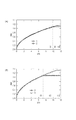
図3に、(13)式で示される拡散係数の比(DX/DY)とAbsmaxの透過率比(T(X)/T(Y))の関係を示す。図3において、縦軸は拡散係数の比(DX/DY)、横軸はXの最大吸光度(Absmax)、また白黒の濃淡は透過率比(T(X)/T(Y))を表す。エレクトロクロミック素子の透過率比の変化が±20%以内の範囲は、図3の1.4で示された白線より下の領域であり、±10%以内の範囲は、図3の1.2で示された白線より下の領域である。 FIG. 3 shows the relationship between the diffusion coefficient ratio (D X / D Y ) expressed by the expression (13) and the transmittance ratio of Abs max (T (X) / T (Y)). In FIG. 3, the vertical axis is the diffusion coefficient ratio (D X / D Y ), the horizontal axis is the maximum X absorbance (Abs max ), and the black and white shade is the transmittance ratio (T (X) / T (Y)). Represents. The range where the change in transmittance ratio of the electrochromic element is within ± 20% is a region below the white line indicated by 1.4 in FIG. 3, and the range within ± 10% is 1.2 in FIG. It is an area below the white line indicated by.
したがって、(13)式と図3より、X、Y分子うち、小さな拡散係数(Dmin(DY))をもつ分子と、大きな拡散係数(Dmax(DX))をもつ分子との拡散係数の関係、Dmaxをもつ分子の与える最大の吸光度Hの関係が、下記式(5)を満たす場合に、透過率は式(14)となり、エレクトロクロミック素子の透過率変化が小さく、下記式(15)を満たす場合に、透過率は式(16)となり、エレクトロクロミック素子の透過率変化がより小さいことがわかる。
1≦D2max/D2min≦(1+0.146/H2) (5)
T(X)/T(Y)≦1.4 (14)
1≦D2max/D2min≦(1+0.0792/H2) (15)
T(X)/T(Y)≦1.2 (16)
Therefore, from the equation (13) and FIG. 3, the diffusion coefficient of a molecule having a small diffusion coefficient (Dmin (D Y )) and a molecule having a large diffusion coefficient (Dmax (D X )) among the X and Y molecules. When the relationship between the relationship and the maximum absorbance H given by the molecule having Dmax satisfies the following formula (5), the transmittance becomes formula (14), and the change in transmittance of the electrochromic device is small. When the above condition is satisfied, the transmittance is expressed by Equation (16), which indicates that the change in transmittance of the electrochromic element is smaller.
1 ≦ D 2 max / D 2 min ≦ (1 + 0.146 / H 2 ) (5)
T (X) / T (Y) ≦ 1.4 (14)
1 ≦ D 2 max / D 2 min ≦ (1 + 0.0792 / H 2 ) (15)
T (X) / T (Y) ≦ 1. 2 (16)
上記の記載では、エレクトロクロミック層に含まれる分子のうち、吸光度への影響が大きい分子である最大吸光度が大きい順に2種類選択した分子、X、Yの関係が式(1)を満たす場合にエレクトロクロミック素子の透過率変化が小さいことを示した。 In the above description, among the molecules contained in the electrochromic layer, two types of molecules selected in descending order of the maximum absorbance, which is a molecule having a large influence on the absorbance, and when the relationship between X and Y satisfies the formula (1), It was shown that the change in transmittance of the chromic element is small.
エレクトロクロミック層に含まれる複数種類の同極性のエレクトロクロミック分子が3種類以上である場合には、エレクトロクロミック層の着色時に、エレクトロクロミック層に含まれる複数種類の同極性のエレクトロクロミック分子のうちの最大吸光度が大きい順に3種類の分子を選択し、それらの分子が各々有する拡散係数のうち、最も小さい拡散係数をDy、最も大きい拡散係数をDx、前記3種類の分子のうちの前記Dxを有する分子の最大吸光度をHとした時に、Dx、Dy、Hが上記式(5)を満たすことが好ましく、より好ましくはそれらが(15)を満たすことである。 When there are three or more types of electrochromic molecules of the same polarity contained in the electrochromic layer, when coloring the electrochromic layer, the electrochromic layer includes a plurality of types of electrochromic molecules of the same polarity contained in the electrochromic layer. Three kinds of molecules are selected in descending order of maximum absorbance, and among these diffusion coefficients, the smallest diffusion coefficient is Dy, the largest diffusion coefficient is Dx, and the three kinds of molecules are Dx. When the maximum absorbance of the molecule is H, Dx, Dy, and H preferably satisfy the above formula (5), and more preferably they satisfy (15).
これは、すなわち、エレクトロクロミック層に複数種類の同極性のエレクトロクロミック分子として3種類以上の同極性のエレクトロクロミック分子を有し、前記エレクトロクロミック層の着色時に前記複数種類の同極性のエレクトロクロミック分子のうち最大吸光度が大きい順に3種類の分子を選択した時に、前記3種類の分子各々の、前記エレクトロクロミック層の着色時における拡散係数のうち、最も小さな拡散係数D3min、最も大きな拡散係数D3max、前記3種類の分子のうち拡散係数が前記D3maxである分子の前記エレクトロクロミック層の着色時の最大吸光度をH3が、下記式(5a)を満たすことが好ましく、より好ましくは、下記式(15a)を満たすということである。
1≦D3max/D3min≦(1+0.146/H3)2 (5a)
1≦D3max/Dmin≦(1+0.0792/H3) (15a)
That is, the electrochromic layer has three or more types of electrochromic molecules having the same polarity as the plurality of types of electrochromic molecules having the same polarity, and the plurality of types of electrochromic molecules having the same polarity are colored when the electrochromic layer is colored. When the three types of molecules are selected in descending order of the maximum absorbance, the smallest diffusion coefficient D 3 min and the largest diffusion coefficient D among the diffusion coefficients of the three kinds of molecules when coloring the electrochromic layer are shown. 3 max, it is preferable that the maximum absorbance at the time of coloring of the electrochromic layer of the molecule having a diffusion coefficient of D 3 max among the three kinds of molecules, H 3 satisfies the following formula (5a), more preferably In other words, the following equation (15a) is satisfied.
1 ≦ D 3 max / D 3 min ≦ (1 + 0.146 / H 3 ) 2 (5a)
1 ≦ D 3 max / Dmin ≦ (1 + 0.0792 / H 3 ) (15a)
さらに、エレクトロクロミック層の着色時に、エレクトロクロミック層に含まれる複数種類の同極性のエレクトロクロミック分子のうちの最大吸光度が最も大きい分子、最大吸光度が最も大きい分子の最大吸光度の1/10以上の最大吸光度を有する分子群のうちの任意の一つの分子、の各々の拡散係数のうちの小さい方の拡散係数をDy、大きい方の拡散係数をDx、前記分子のうちの前記Dxを有する分子のエレクトロクロミック層の着色時の最大吸光度をHとした時に、Dx、Dy、Hが上記式(5)を満たすことが好ましく、より好ましくはそれらが式(15)を満たすことである。 Furthermore, at the time of coloring the electrochromic layer, a molecule having the largest maximum absorbance among the plurality of types of electrochromic molecules of the same polarity contained in the electrochromic layer, a maximum of 1/10 or more of the maximum absorbance of the molecule having the largest maximum absorbance. The smaller diffusion coefficient of each diffusion coefficient of any one molecule in the molecular group having absorbance is Dy, the larger diffusion coefficient is Dx, and the electro of the molecule having the Dx of the molecules When the maximum absorbance at the time of coloring the chromic layer is H, Dx, Dy, and H preferably satisfy the above formula (5), and more preferably they satisfy the formula (15).
これは、すなわち、エレクトロクロミック層に複数種類の同極性のエレクトロクロミック分子のうちの最大吸光度が最も大きい分子、該最大吸光度が最も大きい分子の最大吸光度の1/10以上の最大吸光度を有する分子群のうちの任意の一つの分子、の各々の拡散係数のうちの小さい方の拡散係数をDNmin、大きい方の拡散係数をDNmax、前記分子のうちの前記DNmaxを有する分子のエレクトロクロミック層の着色時の最大吸光度をHNとした時に、下記式(5b)を満たすことが好ましく、より好ましくは、下記式(15b)を満たすということである。
1≦DNmax/DNmin≦(1+0.146/HN)2 (5b)
1≦DNmax/DNmin≦(1+0.0792/HN) (15b)
That is, a molecule group having a maximum absorbance in the electrochromic layer having a maximum maximum absorbance among a plurality of types of electrochromic molecules of the same polarity, and a maximum absorbance of 1/10 or more of the maximum absorbance of the molecule having the maximum maximum absorbance. The smaller diffusion coefficient of each of the numerators of one of the molecules is DN min, the larger diffusion coefficient is DN max, and the molecules having the DN max of the molecules the maximum absorbance of the colored state of the electrochromic layer when the H N, it is preferable to satisfy the following formula (5b), more preferably, is that satisfies the following formula (15b).
1 ≦ D N max / D N min ≦ (1 + 0.146 / H N ) 2 (5b)
1 ≦ D N max / D N min ≦ (1 + 0.0792 / H N ) (15b)
このようにすることにより、エレクトロクロミック層における吸光度に影響を与える分子間の拡散性の差異を小さくすることができ、エレクトロクロミック素子の色バランスを良好にすることができるからである。 By doing in this way, the difference in the diffusibility between the molecules which affects the light absorbency in an electrochromic layer can be made small, and the color balance of an electrochromic element can be made favorable.
なお、このような場合、D2minとD2max、D3minとD3maxが等しい、DNminとDNmaxが等しい場合が含まれる。 In such a case, a case where D 2 min and D 2 max are equal, D 3 min and D 3 max are equal, and D N min and D N max are equal is included.
エレクトロクロミック分子の拡散係数は、既知の電気化学的手法で測定することができる。測定法の例としては、ポテンシャルステップ法による測定を挙げることができる。以下にポシャルステップ法の測定例としてクロノアンペロメトリーによる拡散係数の測定方法について記述する。 The diffusion coefficient of electrochromic molecules can be measured by known electrochemical techniques. As an example of the measurement method, measurement by the potential step method can be mentioned. In the following, a measurement method of the diffusion coefficient by chronoamperometry will be described as an example of measurement of the potential step method.
支持塩を含んだ溶液(例えば0.2Mテトラブチルアンモニウムヘキサフルオロフォスフェートの炭酸プロピレン溶液)に1mM程度のエレクトロクロミック分子を溶解させ、不活性ガスでバブリングし溶存酸素を除く。作用電極(例えばグラッシーカーボン電極)、対電極(例えば白金電極)、参照電極(例えばAg/Ag+電極)を用いた三極セルに先の溶液を導入する。作用電極に、あらかじめサイクリックボルタンモグラム等で決定しておいた、着色体を生成させるのに十分な電位を印加し、流れる電流を数十秒程度測定する。流れた電流の時間応答は、式(5)に従うので、測定した過渡電流を経過時間の平方根の逆数に対してプロットし、その傾きから拡散係数を算出することができる。 About 1 mM electrochromic molecules are dissolved in a solution containing a supporting salt (for example, 0.2 M tetrabutylammonium hexafluorophosphate in propylene carbonate), and the dissolved oxygen is removed by bubbling with an inert gas. The previous solution is introduced into a triode cell using a working electrode (for example, a glassy carbon electrode), a counter electrode (for example, a platinum electrode), and a reference electrode (for example, an Ag / Ag + electrode). A potential sufficient to generate a colored body, which has been previously determined by a cyclic voltammogram or the like, is applied to the working electrode, and the flowing current is measured for several tens of seconds. Since the time response of the flowing current follows equation (5), the measured transient current is plotted against the reciprocal of the square root of the elapsed time, and the diffusion coefficient can be calculated from the slope.
本実施形態のエレクトロクロミック素子を可視光領域の撮像装置における光量調整手段(NDフィルタ)として使用する場合を想定した場合のDmax/Dminの好ましい範囲を以下に具体的に示す。なお、本実施形態において、消色状態の透過率と比較して、6分の1の透過率にすることを6段の透過率と表現する。すなわち、n段の透過率とは消色状態と比較して、n分の1の透過率とすることである。 The preferable range of Dmax / Dmin when the case where the electrochromic element of this embodiment is used as a light amount adjusting means (ND filter) in an imaging device in the visible light region is specifically shown below. Note that, in this embodiment, setting the transmittance to 1/6 compared with the transmittance in the decolored state is expressed as six-stage transmittance. In other words, the n-stage transmittance means that the transmittance is 1 / n compared with the decolored state.
半値全幅160nm、ピーク波長300、400、500、600、700、800の6種の正規分布の吸収スペクトルを用いて425nm〜700nm間に6段(T=0.0156)の透過率を成立させる最大吸光度(Absmax)を計算すると、1.08となる。この条件における透過率比の変化が±20%以内となるDmax/Dminは、(12)式より、
Dmax/Dmin≦1.29 (17)
を満たし、
透過率比の変化が±10%以内となるDmax/Dminは、
Dmax/Dmin≦1.15 (18)
を満たす。
Maximum to establish a transmittance of 6 steps (T = 0.0156) between 425 nm and 700 nm using six types of normal distribution absorption spectra of full width at half maximum of 160 nm and peak wavelengths of 300, 400, 500, 600, 700, 800 The absorbance (Abs max ) is calculated to be 1.08. Dmax / Dmin at which the change in the transmittance ratio under these conditions is within ± 20% is obtained from the equation (12):
Dmax / Dmin ≦ 1.29 (17)
The filling,
Dmax / Dmin at which the change in transmittance ratio is within ± 10% is
Dmax / Dmin ≦ 1.15 (18)
Meet.
すなわち、X、Y分子うち、小さな拡散係数(Dmin(DY))をもつ分子と、大きな拡散係数(Dmax(DX))をもつ分子との拡散係数の関係を上記範囲とすることで、各々、透過率比の変化が±20%以内、±10%以内のエレクトロクロミック素子とすることができる。 That is, among the X and Y molecules, by setting the relationship between the diffusion coefficient of a molecule having a small diffusion coefficient (Dmin (D Y )) and a molecule having a large diffusion coefficient (Dmax (D X )) within the above range, Each can be an electrochromic element having a change in transmittance ratio within ± 20% and within ± 10%.
この際、前述した場合と同様、DmaxおよびDminは、
(i)エレクトロクロミック層の着色時に前記複数種類の同極性のエレクトロクロミック分子のうち最大吸光度が大きい順に2種類の分子を選択した時に、前記2種類の分子各々の、前記エレクトロクロミック層の着色時における拡散係数のうち、小さい方の拡散係数D2minおよび大きい方の拡散係数D2maxであっても良い。
At this time, as in the case described above, Dmax and Dmin are
(I) When the electrochromic layer is colored, when two types of molecules are selected in descending order of the maximum absorbance among the plurality of types of electrochromic molecules having the same polarity, the electrochromic layer is colored for each of the two types of molecules. The smaller diffusion coefficient D 2 min and the larger diffusion coefficient D 2 max may be used.
(ii)また、エレクトロクロミック層の着色時に前記複数種類の同極性のエレクトロクロミック分子のうち最大吸光度が大きい順に3種類の分子を選択した時に、前記3種類の分子各々の、前記エレクトロクロミック層の着色時における拡散係数のうち、最も小さな拡散係数D3minおよび最も大きな拡散係数D3maxであっても良い。 (Ii) In addition, when three types of molecules are selected in descending order of maximum absorbance among the plurality of types of electrochromic molecules having the same polarity when the electrochromic layer is colored, each of the three types of molecules has the electrochromic layer Of the diffusion coefficients during coloring, the smallest diffusion coefficient D 3 min and the largest diffusion coefficient D 3 max may be used.
更に、
(iii)大吸光度が最も大きい分子の最大吸光度の1/10以上の最大吸光度を有する分子群のうちの任意の一つの分子、の各々の拡散係数のうちの小さい方の拡散係数をDNmin、大きい方の拡散係数をDNmaxおよび前記分子のうちの前記DNmaxでも良い。
Furthermore,
(Iii) D N min is the smaller diffusion coefficient of each diffusion coefficient of any one molecule in the molecule group having the maximum absorbance of 1/10 or more of the maximum absorbance of the molecule having the largest large absorbance. good diffusion coefficients larger even the D N max of the D N max and the molecule.
すなわち、そのような場合、
(i)では、透過率比の変化が±20%以内では、
1≦D2max/D2min≦1.29 (17)
を満たし、透過率比の変化が±10%以内では
1≦D2max/D2min≦1.15 (18)
を満たすことになる。
That is, in such a case,
In (i), if the change in transmittance ratio is within ± 20%,
1 ≦ D 2 max / D 2 min ≦ 1.29 (17)
1 ≦ D 2 max / D 2 min ≦ 1.15 when the change in transmittance ratio is within ± 10% (18)
Will be satisfied.
また、(ii)では、透過率比の変化が±20%以内では、
1≦D3max/D3min≦1.29 (17a)
を満たし、透過率比の変化が±10%以内では
1≦D3max/D3min≦1.15 (18a)
を満たすことになる。
In (ii), if the change in transmittance ratio is within ± 20%,
1 ≦ D 3 max / D 3 min ≦ 1.29 (17a)
1 ≦ D 3 max / D 3 min ≦ 1.15 (18a) when the change in transmittance ratio is within ± 10%.
Will be satisfied.
更に、(iii)では、透過率比の変化が±20%以内では、
1≦DNmax/DNmin≦1.29 (17b)
を満たし、透過率比の変化が±10%以内では
1≦DNmax/DNmin≦1.15 (18b)
を満たすことになる。
Furthermore, in (iii), if the change in transmittance ratio is within ± 20%,
1 ≦ D N max / D N min ≦ 1.29 (17b)
1 ≦ DN max / DN min ≦ 1.15 (18b) when the change in transmittance ratio is within ± 10%.
Will be satisfied.
(4)用途等
本実施形態のエレクトロクロミック素子は、光学フィルタ、レンズユニット、撮像装置に用いることができる。具体的には、エレクトロクロミック素子を撮像素子につながる撮像光学系の光路内に設けることにより、撮像素子が受光する光量もしくは入射光の波長分布特性を制御することができる。この撮像光学系は、レンズ系ともいうことができる。撮像光学系の例としては、複数のレンズを有するレンズユニット等が挙げられる。
(4) Use etc. The electrochromic element of this embodiment can be used for an optical filter, a lens unit, and an imaging device. Specifically, by providing the electrochromic element in the optical path of the imaging optical system connected to the imaging element, the light quantity received by the imaging element or the wavelength distribution characteristic of incident light can be controlled. This imaging optical system can also be called a lens system. Examples of the imaging optical system include a lens unit having a plurality of lenses.
また、本実施形態のエレクトロクロミック素子は、トランジスタ等と接続することによって、電気的に制御された光学フィルタとして機能する。トランジスタとしては、例えば、TFT素子やMIM素子等が挙げられる。 Moreover, the electrochromic element of this embodiment functions as an electrically controlled optical filter by being connected to a transistor or the like. Examples of the transistor include a TFT element and an MIM element.
ここで記載する撮像装置は、撮像素子と光学フィルタを有する撮像光学系とを有するものである。また、本実施形態のエレクトロクロミック素子が撮像装置に用いられる場合、エレクトロクロミック素子の配置される位置は問われない。例えば、撮像光学系の前であっても、撮像素子の直前であってもよい。 The imaging apparatus described here includes an imaging element and an imaging optical system having an optical filter. Moreover, when the electrochromic element of this embodiment is used for an imaging device, the position where an electrochromic element is arrange | positioned is not ask | required. For example, it may be in front of the imaging optical system or immediately before the imaging element.
エレクトロクロミック素子が消色状態では高透明性を発揮できるので、入射光に対して充分な透過光量が得られ、また着色状態では入射光を確実に遮光及び変調した光学的特性が得られる。 Since the electrochromic element can exhibit high transparency when it is decolored, a sufficient amount of transmitted light can be obtained with respect to the incident light, and in the colored state, optical characteristics can be obtained in which the incident light is reliably blocked and modulated.
以下、実施例により本発明をさらに具体的に説明していくが、本発明はこれらに限定されるものではない。 EXAMPLES Hereinafter, the present invention will be described more specifically with reference to examples, but the present invention is not limited to these examples.
実施例のエレクトロクロミック分子の合成について記述する。 The synthesis of the electrochromic molecules of the examples is described.
なお、以降の実施例においては、エレクトロクロミック分子をEC分子、エレクトロクロミック素子をEC素子、エレクトロクロミック層をEC層と表記する場合がある。 In the following examples, electrochromic molecules may be referred to as EC molecules, electrochromic elements as EC elements, and electrochromic layers as EC layers.
[合成例1]
例示化合物1(EC分子1)の合成
[Synthesis Example 1]
Synthesis of exemplary compound 1 (EC molecule 1)
(1)100mlの反応容器で、XX−1(3,4−ジメチルチオフェン):2.55g(22.7mmol)をジエチルエーテル30mlに溶解し、−78℃に冷却した。 (1) In a 100 ml reaction vessel, XX-1 (3,4-dimethylthiophene): 2.55 g (22.7 mmol) was dissolved in 30 ml of diethyl ether and cooled to -78 ° C.
この溶液にn−ブチルリチウム(1.62Mヘキサン溶液)18.2mlを滴下し−78℃で1時間攪拌した。 To this solution, 18.2 ml of n-butyllithium (1.62 M hexane solution) was added dropwise and stirred at -78 ° C for 1 hour.
次いで、2−イソプロポキシ−4,4,5,5−テトラメチル−1,3,2−ジオキサボロラン5.92g(31.8mmol)を添加し、さらに30分後、反応溶液を室温に戻し、そのまま室温で2時間撹拌した。 Subsequently, 2-isopropoxy-4,4,5,5-tetramethyl-1,3,2-dioxaborolane (5.92 g, 31.8 mmol) was added, and after another 30 minutes, the reaction solution was returned to room temperature and left as it was. Stir at room temperature for 2 hours.
塩化アンモニウム水溶液を加え反応を停止した後、ジイソプロピルエーテルで抽出・水洗し、エーテル層を減圧濃縮し粗生成物を得た。 An aqueous ammonium chloride solution was added to stop the reaction, followed by extraction with diisopropyl ether and washing with water. The ether layer was concentrated under reduced pressure to obtain a crude product.
シリカゲルクロマトグラフィー(移動相:ヘプタン/トルエン=1/1)により分離精製し、無色液体のXX−2を得た。 Separation and purification by silica gel chromatography (mobile phase: heptane / toluene = 1/1) gave colorless liquid XX-2.
(2)200ml反応容器に、XX−2:4.62g(ca.10mmol)、XX−3:2.96g(15.5mmol)をトルエン/エタノール/蒸留水(25ml/13ml/25ml)混合溶媒で混合し、窒素で溶存酸素を除去した。 (2) In a 200 ml reaction vessel, XX-2: 4.62 g (ca. 10 mmol) and XX-3: 2.96 g (15.5 mmol) were mixed with toluene / ethanol / distilled water (25 ml / 13 ml / 25 ml) mixed solvent. Mix and remove dissolved oxygen with nitrogen.
次いで、Pd(PPh3)4:0.27g(0.233mmol)および炭酸ナトリウム:2.5g(23.3mmol)を窒素雰囲気下添加した後、90℃で21時間、加熱反応を行った。 Next, Pd (PPh 3 ) 4 : 0.27 g (0.233 mmol) and sodium carbonate: 2.5 g (23.3 mmol) were added under a nitrogen atmosphere, and a heating reaction was performed at 90 ° C. for 21 hours.
反応溶液を室温まで冷却後、減圧濃縮し、シリカゲルクロマトグラフィー(移動相:ヘプタン)により分離精製し、XX−4を得た(1.0g)。 The reaction solution was cooled to room temperature, concentrated under reduced pressure, and separated and purified by silica gel chromatography (mobile phase: heptane) to obtain XX-4 (1.0 g).
(3)100mLの反応容器で、XX−4:1.30g(5.86mmol)をDMF40mlに溶解した。次いで、N−ブロモスクシンイミド:2.71g(15.2mmol)を加え、室温で6時間撹拌した。 (3) In a 100 mL reaction vessel, 1.30 g (5.86 mmol) of XX-4 was dissolved in 40 ml of DMF. Next, N-bromosuccinimide: 2.71 g (15.2 mmol) was added, and the mixture was stirred at room temperature for 6 hours.
反応溶液に水を加え、析出物をメタノールで分散洗浄を行った後、濾別し、XX−5を得た(1.97g)
(4)100ml反応容器に、XX−5:464mg(1.22mmol),2−イソプロポキシ−6−メトキシフェニルボロン酸:771mg(3.67mmol)を、トルエン/テトラヒドロフラン(6ml/6ml)混合溶媒中で混合し、窒素で溶存酸素を除去した。
Water was added to the reaction solution, and the precipitate was dispersed and washed with methanol and then filtered to obtain XX-5 (1.97 g).
(4) XX-5: 464 mg (1.22 mmol), 2-isopropoxy-6-methoxyphenylboronic acid: 771 mg (3.67 mmol) in a 100 ml reaction vessel in a toluene / tetrahydrofuran (6 ml / 6 ml) mixed solvent And dissolved oxygen was removed with nitrogen.
次にPd(OAc)2:11.0mg(0.049mmol)、2−ジシクロヘキシルフォスフィノ−2’,6’−ジメトキシビフェニル(S−Phos):50mg(0.122mmol)、りん酸三カリウム:1.41g(6.12mmol)を窒素雰囲気下添加し、110℃にて加熱還流し13時間反応を行った。 Next, Pd (OAc) 2 : 11.0 mg (0.049 mmol), 2-dicyclohexylphosphino-2 ′, 6′-dimethoxybiphenyl (S-Phos): 50 mg (0.122 mmol), tripotassium phosphate: 1 .41 g (6.12 mmol) was added under a nitrogen atmosphere, and the mixture was heated to reflux at 110 ° C. and reacted for 13 hours.
反応溶液を室温まで冷却後、減圧濃縮し、シリカゲルクロマトグラフィー(移動相:ヘキサン/クロロホルム=1/3)により分離精製し、白色固体粉末の1を得た(29mg)。 The reaction solution was cooled to room temperature, concentrated under reduced pressure, and separated and purified by silica gel chromatography (mobile phase: hexane / chloroform = 1/3) to obtain a white solid powder 1 (29 mg).
MALDI−MS測定により、この化合物のM+である524を確認した。またNMRスペクトルの測定結果を以下に示す。
1H−NMR(CDCl3)σ(ppm):7.24(t,2H),6.64(d,2H),6.61(d,2H),4.35(sept,2H),3.79(s,6H),2.14(s,6H),1.94(s,6H),1.23(d,6H),1.18(d,6H).
524 which is M <+> of this compound was confirmed by the MALDI-MS measurement. Moreover, the measurement result of a NMR spectrum is shown below.
1 H-NMR (CDCl 3 ) σ (ppm): 7.24 (t, 2H), 6.64 (d, 2H), 6.61 (d, 2H), 4.35 (sept, 2H), 3 79 (s, 6H), 2.14 (s, 6H), 1.94 (s, 6H), 1.23 (d, 6H), 1.18 (d, 6H).
[合成例2]
例示化合物2(EC分子2)の合成
[Synthesis Example 2]
Synthesis of exemplary compound 2 (EC molecule 2)
(1)50mLの反応容器で、XX−6:300mg(1.24mmol)、XX−7:1.10g(3.72mmol)をトルエン/テトラヒドロフラン(8ml/4ml)混合溶媒中で混合し、窒素で溶存酸素を除去した。次にPd(OAc)2:8.4mg(0.037mmol)、2−ジシクロヘキシルフォスフィノ−2’,6’−ジメトキシビフェニル(S−Phos):40.7mg(0.0992mmol)およびりん酸三カリウム:1.43g(6.2mmol)を窒素雰囲気下添加し、110℃にて加熱還流し7時間反応を行った。反応溶液を室温まで冷却後、減圧濃縮し、シリカゲルクロマトグラフィー(移動相:ヘキサン)により分離精製し、無色粘調液体のXX−8を得た(360mg、収率70%)。 (1) In a 50 mL reaction vessel, XX-6: 300 mg (1.24 mmol) and XX-7: 1.10 g (3.72 mmol) were mixed in a toluene / tetrahydrofuran (8 ml / 4 ml) mixed solvent, and nitrogen was added. Dissolved oxygen was removed. Next, Pd (OAc) 2 : 8.4 mg (0.037 mmol), 2-dicyclohexylphosphino-2 ′, 6′-dimethoxybiphenyl (S-Phos): 40.7 mg (0.0992 mmol) and tripotassium phosphate : 1.43 g (6.2 mmol) was added under a nitrogen atmosphere, and the mixture was heated to reflux at 110 ° C. and reacted for 7 hours. The reaction solution was cooled to room temperature, concentrated under reduced pressure, and separated and purified by silica gel chromatography (mobile phase: hexane) to obtain a colorless viscous liquid XX-8 (360 mg, yield 70%).
(2)100mLの反応容器で、(1)で得られたXX−8:355mg(0.852mmol)をDMF(N,N−ジメチルフォルムアミド)25mlに溶解した。次いで、N−ブロモスクシンイミド:333mg(1.87mmol)を加え、室温で8時間撹拌した。反応溶液に水を加え、クロロホルムで抽出・水洗後、減圧濃縮し、XX−9を得た(470mg、収率96%)。 (2) XX-8: 355 mg (0.852 mmol) obtained in (1) was dissolved in 25 ml of DMF (N, N-dimethylformamide) in a 100 mL reaction vessel. Next, N-bromosuccinimide: 333 mg (1.87 mmol) was added, and the mixture was stirred at room temperature for 8 hours. Water was added to the reaction solution, extracted with chloroform, washed with water, and concentrated under reduced pressure to obtain XX-9 (470 mg, yield 96%).
(3)50mlの反応容器で、XX−9:470mg(0.818mmol)、2−イソプロポキシ−6−メトキシフェニルボロン酸:515mg(2.45mmol)をトルエン/テトラヒドロフラン(5ml/2.5ml)混合溶媒中で混合し、窒素で溶存酸素を除去した。次にPd(OAc)2:5.5mg(0.0245mmol)、2−ジシクロヘキシルフォスフィノ−2’,6’−ジメトキシビフェニル(S−Phos):27mg(0.065mmol)およびりん酸三カリウム:942mg(4.09mmol)を窒素雰囲気下添加し、加熱還流し7時間反応を行った。反応溶液を室温まで冷却後、減圧濃縮し、シリカゲルクロマトグラフィー(移動相:ヘキサン/クロロホルム=1/2)により分離精製し、淡黄色固体の2を得た(520mg、収率85%)。 (3) XX-9: 470 mg (0.818 mmol), 2-isopropoxy-6-methoxyphenylboronic acid: 515 mg (2.45 mmol) in toluene / tetrahydrofuran (5 ml / 2.5 ml) in a 50 ml reaction vessel Mix in solvent and remove dissolved oxygen with nitrogen. Next, Pd (OAc) 2 : 5.5 mg (0.0245 mmol), 2-dicyclohexylphosphino-2 ′, 6′-dimethoxybiphenyl (S-Phos): 27 mg (0.065 mmol) and tripotassium phosphate: 942 mg (4.09 mmol) was added under a nitrogen atmosphere, and the mixture was heated to reflux and reacted for 7 hours. The reaction solution was cooled to room temperature, concentrated under reduced pressure, and separated and purified by silica gel chromatography (mobile phase: hexane / chloroform = 1/2) to obtain 2 as a pale yellow solid (520 mg, yield 85%).
実施例1と同様にNMRおよびMALDI−MS測定により、この化合物の構造確認を行った。MALDI−MS測定により、この化合物のM+である744を確認した。またNMRスペクトルの測定結果を以下に示す。
1H−NMR(CDCl3)σ(ppm):7.27(t,2H),7.06(s,2H),7.01(s,2H),6.62(d,2H),6.59(d,2H),4.43(m,2H),3.77(s,6H),2.31(t,4H),1.53(m,4H),1.32−1.10(m,24H),0.84(t,6H).
13C−NMR(CDCl3)σ(ppm):159.15,157.53,141.83,136.37,135.99,129.51,128.33,124.36,123.29,112.85,107.51,103.63,71.09,55.86,31.74,29.97,29.21,29.11,22.61,22.13,22.08,14.13.
The structure of this compound was confirmed by NMR and MALDI-MS measurements in the same manner as in Example 1. 744 which is M <+> of this compound was confirmed by the MALDI-MS measurement. Moreover, the measurement result of a NMR spectrum is shown below.
1 H-NMR (CDCl 3 ) σ (ppm): 7.27 (t, 2H), 7.06 (s, 2H), 7.01 (s, 2H), 6.62 (d, 2H), 6 .59 (d, 2H), 4.43 (m, 2H), 3.77 (s, 6H), 2.31 (t, 4H), 1.53 (m, 4H), 1.32-1. 10 (m, 24H), 0.84 (t, 6H).
13 C-NMR (CDCl 3 ) σ (ppm): 159.15, 157.53, 141.83, 136.37, 135.99, 129.51, 128.33, 124.36, 123.29, 112 85, 107.51, 103.63, 71.09, 55.86, 31.74, 29.97, 29.21, 29.11, 22.61, 22.21, 22.08, 14.13 .
[合成例3]
例示化合物3(EC分子3)の合成
[Synthesis Example 3]
Synthesis of exemplary compound 3 (EC molecule 3)
50mlの反応容器で、XX−10(2,5−ジブロモエチレンジオキシチオフェン):500mg(1.67mmol)、2−イソプロポキシ−6−メトキシフェニルボロン酸:1.05g(5.0mmol)を、トルエン/テトラヒドロフラン(10ml/5ml)混合溶媒中で混合し、窒素で溶存酸素を除去した。 In a 50 ml reaction vessel, XX-10 (2,5-dibromoethylenedioxythiophene): 500 mg (1.67 mmol), 2-isopropoxy-6-methoxyphenylboronic acid: 1.05 g (5.0 mmol), The mixture was mixed in a toluene / tetrahydrofuran (10 ml / 5 ml) mixed solvent, and dissolved oxygen was removed with nitrogen.
次にPd(OAc)2:19mg(0.083mmol)、2−ジシクロヘキシルフォスフィノ−2’,6’−ジメトキシビフェニル(S−Phos):89mg(0.22mmol)およびりん酸三カリウム:1.92g(8.35mmol)を窒素雰囲気下添加し、110℃にて加熱還流し7時間反応を行った。 Next, Pd (OAc) 2 : 19 mg (0.083 mmol), 2-dicyclohexylphosphino-2 ′, 6′-dimethoxybiphenyl (S-Phos): 89 mg (0.22 mmol) and tripotassium phosphate: 1.92 g (8.35 mmol) was added under a nitrogen atmosphere, and the mixture was heated to reflux at 110 ° C. and reacted for 7 hours.
反応溶液を室温まで冷却後、減圧濃縮し、シリカゲルクロマトグラフィー(移動相:ヘキサン/酢酸エチル=4/3)により分離精製し、白色固体粉末の3を得た(420mg、収率54%)。 The reaction solution was cooled to room temperature, concentrated under reduced pressure, and separated and purified by silica gel chromatography (mobile phase: hexane / ethyl acetate = 4/3) to obtain a white solid powder 3 (420 mg, yield 54%).
合成例1と同様にMALDI−MS測定により、この化合物のM+である470を確認した。またNMRスペクトルの測定結果を以下に示す。
1H−NMR(CDCl3)σ(ppm):7.21(t,2H),6.63(d,2H),6.60(d,2H),4.41(m,2H),4.20(s,4H),3.81(s,6H),1.25(s,6H),1.24(s,6H).
470 which is M + of this compound was confirmed by MALDI-MS measurement in the same manner as in Synthesis Example 1. Moreover, the measurement result of a NMR spectrum is shown below.
1 H-NMR (CDCl 3 ) σ (ppm): 7.21 (t, 2H), 6.63 (d, 2H), 6.60 (d, 2H), 4.41 (m, 2H), 4 .20 (s, 4H), 3.81 (s, 6H), 1.25 (s, 6H), 1.24 (s, 6H).
[合成例4]
例示化合物4(EC分子4)の合成
[Synthesis Example 4]
Synthesis of exemplary compound 4 (EC molecule 4)
50mlの反応容器で、XX−11:177.05mg(0.50mmol)、2−イソプロポキシ−6−メトキシフェニルボロン酸:420mg(2.0mmol)を、トルエン/テトラヒドロフラン(6ml/3ml)混合溶媒中で混合し、窒素で溶存酸素を除去した。 In a 50 ml reaction vessel, XX-11: 177.05 mg (0.50 mmol), 2-isopropoxy-6-methoxyphenylboronic acid: 420 mg (2.0 mmol) in a toluene / tetrahydrofuran (6 ml / 3 ml) mixed solvent And dissolved oxygen was removed with nitrogen.
次にPd(OAc)2:2.3mg(0.01mmol)、2−ジシクロヘキシルフォスフィノ−2’,6’−ジメトキシビフェニル(S−Phos):10.3mg(0.025mmol)およびりん酸三カリウム:575.7mg(2.5mmol)を窒素雰囲気下添加し、110℃にて加熱還流し8時間反応を行った。 Next, Pd (OAc) 2 : 2.3 mg (0.01 mmol), 2-dicyclohexylphosphino-2 ′, 6′-dimethoxybiphenyl (S-Phos): 10.3 mg (0.025 mmol) and tripotassium phosphate : 575.7 mg (2.5 mmol) was added under a nitrogen atmosphere, and the mixture was heated to reflux at 110 ° C. and reacted for 8 hours.
反応溶液を室温まで冷却後、減圧濃縮し、シリカゲルクロマトグラフィー(移動相:ヘキサン/クロロホルム=1/2)により分離精製し、白色固体粉末の4を得た(187mg、収率71%)。MALDI−MS測定により、この化合物のM+である524を確認した。 The reaction solution was cooled to room temperature, concentrated under reduced pressure, and separated and purified by silica gel chromatography (mobile phase: hexane / chloroform = 1/2) to obtain white solid powder 4 (187 mg, yield 71%). 524 which is M <+> of this compound was confirmed by the MALDI-MS measurement.
素子の作製について記述する。 The device fabrication is described.
例示化合物5(EC分子5)の合成 Synthesis of exemplary compound 5 (EC molecule 5)
(1)300mLの反応容器で、XX−1(3,4−ジメチルチオフェン):5.0g(44.6mmol)をDMF(N,N−ジメチルフォルムアミド)80mlに溶解した。次いで、N−ブロモスクシンイミド:31.7g(178mmol)を加え、室温で1時間撹拌した。反応溶液に水を加え、ジエチルエーテル/ヘキサン(1/1)で抽出・水洗後、減圧濃縮し、XX−11を得た。 (1) XX-1 (3,4-dimethylthiophene): 5.0 g (44.6 mmol) was dissolved in 80 ml of DMF (N, N-dimethylformamide) in a 300 mL reaction vessel. Next, N-bromosuccinimide: 31.7 g (178 mmol) was added, and the mixture was stirred at room temperature for 1 hour. Water was added to the reaction solution, extracted with diethyl ether / hexane (1/1), washed with water, and concentrated under reduced pressure to obtain XX-11.
(2)50ml反応容器に、XX−11:500mg(1.85mmol),2−イソプロポキシ−6−メトキシフェニルボロン酸:1.17g(5.56mmol)を、トルエン/テトラヒドロフラン(5ml/5ml)混合溶媒中で混合し、窒素で溶存酸素を除去した。 (2) XX-11: 500 mg (1.85 mmol), 2-isopropoxy-6-methoxyphenylboronic acid: 1.17 g (5.56 mmol) in toluene / tetrahydrofuran (5 ml / 5 ml) mixed in a 50 ml reaction vessel Mix in solvent and remove dissolved oxygen with nitrogen.
次にPd(OAc)2:16.6mg(0.074mmol)、2−ジシクロヘキシルフォスフィノ−2’,6’−ジメトキシビフェニル(S−Phos):76mg(0.185mmol)、りん酸三カリウム:2.13g(9.26mmol)を窒素雰囲気下添加し、100℃にて加熱還流し6時間反応を行った。 Next, Pd (OAc) 2 : 16.6 mg (0.074 mmol), 2-dicyclohexylphosphino-2 ′, 6′-dimethoxybiphenyl (S-Phos): 76 mg (0.185 mmol), tripotassium phosphate: 2 .13 g (9.26 mmol) was added under a nitrogen atmosphere, and the mixture was heated to reflux at 100 ° C. and reacted for 6 hours.
反応溶液を室温まで冷却後、減圧濃縮し、シリカゲルクロマトグラフィー(移動相:ヘキサン/酢酸エチル=5/2)により分離精製し、無色粘調液体の2を得た。
The reaction solution was cooled to room temperature, concentrated under reduced pressure, and separated and purified by silica gel chromatography (mobile phase: hexane / ethyl acetate = 5/2) to obtain colorless
1と同様にマススペクトル(MS)測定及び核磁気共鳴スペクトル(NMR)測定の測定により、化合物5の構造確認を行った結果、分子量およびNMRピーク積分値の比がその構造と良く一致した。
As in Example 1, the structure of
[作製例]
厚さ1.1mmのガラス基板上に膜厚200nmのフッ素ドープ酸化スズ(FTO)薄膜を形成した透明電極を準備した。このFTO透明電極の可視光平均透過率は85%、またシート抵抗は40Ω/□であった。
[Production example]
A transparent electrode in which a fluorine-doped tin oxide (FTO) thin film having a thickness of 200 nm was formed on a glass substrate having a thickness of 1.1 mm was prepared. This FTO transparent electrode had an average visible light transmittance of 85% and a sheet resistance of 40Ω / □.
次に、平均粒径21nmの酸化スズナノ粒子スラリーと平均粒径34nmの酸化亜鉛ナノ粒子スラリーを酸化スズと酸化亜鉛の体積比が2:1になるように混合調整したものを同じFTO透明電極上に塗布形成し、500℃で30分焼成した後、希塩酸により酸化亜鉛のみをエッチングし多孔質酸化スズナノ粒子膜を得た。この多孔質膜の厚さは、約5.0μmであった。 Next, a tin oxide nanoparticle slurry having an average particle diameter of 21 nm and a zinc oxide nanoparticle slurry having an average particle diameter of 34 nm mixed and adjusted so that the volume ratio of tin oxide and zinc oxide is 2: 1 are mixed on the same FTO transparent electrode. Then, after baking at 500 ° C. for 30 minutes, only zinc oxide was etched with dilute hydrochloric acid to obtain a porous tin oxide nanoparticle film. The thickness of this porous film was about 5.0 μm.
こうして作製したFTO透明電極と多孔質酸化スズナノ粒子膜を、導電面を向かい合わせて溶液の注入口を残し、エポキシ樹脂により接合した。このとき厚さの異なるフィルムまたはビーズをスペーサーとして用い、電極間距離を調整した。この後、素子については、FTO透明電極の方を作用電極として記述する。 The FTO transparent electrode thus produced and the porous tin oxide nanoparticle film were joined together with an epoxy resin with the conductive surfaces facing each other, leaving a solution inlet. At this time, films or beads having different thicknesses were used as spacers to adjust the distance between the electrodes. After this, for the element, the FTO transparent electrode is described as the working electrode.
次に、EC分子と、支持電解質として0.2Mのテトラブチルアンモニウムヘキサフルオロフォスフェートとを炭酸プロピレン溶解し、EC組成物を調製した。 Next, EC molecules and 0.2 M tetrabutylammonium hexafluorophosphate as a supporting electrolyte were dissolved in propylene carbonate to prepare an EC composition.
先に準備した開口部を残して接合した空素子に、真空注入法により開口部からEC組成物を注入してEC層を形成し、さらに開口部をエポキシ樹脂により封止してエレクトロクロミック素子を作製した。 An EC element is formed by injecting an EC composition from the opening by vacuum injection to the empty element that has been prepared while leaving the opening, and the opening is sealed with an epoxy resin to form an electrochromic element. Produced.
本実施例の測定について記載する。 It describes about the measurement of a present Example.
[測定例1]
EC分子の拡散係数の測定について記述する。
[Measurement Example 1]
Describes the measurement of the diffusion coefficient of EC molecules.
EC分子の拡散係数は、クロノアンペロメトリーで測定をおこなった。0.2Mテトラブチルアンモニウムヘキサフルオロフォスフェートの炭酸プロピレン(PC)溶液に、1mMのEC分子を溶解させ、窒素ガスでバブリングし溶存酸素を除いた。直径3mmの平面グラッシーカーボン電極を作用電極、白金を対電極、Ag/Ag+(PF6,PC)を参照電極として用い、EC分子の溶液を導入して測定セルとした。測定は窒素を満たしたグローブボックス中、25℃で行った。最初にサイクリックボルタンモグラムで各EC材料の酸化(カソードEC材料では還元)ピークを与える電位を記録した。クロノアンペロメトリー測定では、酸化(カソードEC材料では還元)電流が流れ始めるより負(カソードEC材料では正)の電位から、先に記録したピーク電位より0.2−0.25V程度さらに正(カソードEC材料では負)側の電位(第一酸化還元電位を十分に超え、第二酸化還元電位を超えない電位)を印加して測定を行った。電流を60秒記録し、その過渡電流を経過時間の平方根の逆数に対してプロットし、その傾きから拡散係数を算出した。 The diffusion coefficient of EC molecules was measured by chronoamperometry. 1 mM EC molecules were dissolved in 0.2 M tetrabutylammonium hexafluorophosphate in propylene carbonate (PC) solution, and dissolved oxygen was removed by bubbling with nitrogen gas. Using a 3 mm diameter planar glassy carbon electrode as a working electrode, platinum as a counter electrode, and Ag / Ag + (PF 6 , PC) as a reference electrode, an EC molecule solution was introduced to form a measurement cell. The measurement was performed at 25 ° C. in a glove box filled with nitrogen. First, the potential giving the oxidation (reduction for cathode EC material) peak of each EC material was recorded in a cyclic voltammogram. In the chronoamperometry measurement, from the negative potential (positive in the cathode EC material) to the beginning of the oxidation (reduction in the cathode EC material) current, it is about 0.2 to 0.25 V more positive than the previously recorded peak potential ( Measurement was performed by applying a potential on the negative side of the cathode EC material (potential that sufficiently exceeded the first oxidation-reduction potential and did not exceed the second oxidation-reduction potential). The current was recorded for 60 seconds, the transient current was plotted against the reciprocal of the square root of the elapsed time, and the diffusion coefficient was calculated from the slope.
表1には、合成例で記述したEC分子1−5に加え、4−ブロモ−4’,4’’−ジメチルトリフェニルアミン(EC分子6)、1−n−ヘプチル−1’−フェニル−4,4’−ビピリジニウムジヘキサフルオロフェスフェート(EC分子7)、ヘプチルビオロゲンジヘキサフルオロフェスフェート(EC分子8)の測定された拡散係数を示す。 In Table 1, in addition to EC molecule 1-5 described in the synthesis example, 4-bromo-4 ′, 4 ″ -dimethyltriphenylamine (EC molecule 6), 1-n-heptyl-1′-phenyl- The measured diffusion coefficients of 4,4′-bipyridinium dihexafluorophosphate (EC molecule 7) and heptyl viologen dihexafluorophosphate (EC molecule 8) are shown.
[測定例2]
EC素子の測定方法について記述する。
[Measurement Example 2]
The measurement method of EC element is described.
作製例に記載した方法で作製したEC素子の電極をポテンショスタットに接続し、着色部に紫外から近赤外にわたる波長領域光を照射、透過光強度を分光器で測定する。実施例1乃至9、11および比較例1および2においては、ポテンショスタットを用いて作用電極に0.32V vs Ag/Ag+(PF6,PC)の電位を印加し、その際の吸収スペクトルを記録する。実施例10においては、作用電極に−1.25Vを印加した以外は他の実施例と同様に測定した。複数のEC材料を用いて作製したEC素子の吸収スペクトルは、あらかじめ各EC材料について単独で測定しておいた吸収スペクトルを用いて分割することで、どのEC材料が着色しているかを計算することができる。 The electrode of the EC element manufactured by the method described in the manufacturing example is connected to a potentiostat, the colored region is irradiated with light in the wavelength region from ultraviolet to near infrared, and the transmitted light intensity is measured with a spectroscope. In Examples 1 to 9, 11 and Comparative Examples 1 and 2, a potential of 0.32 V vs Ag / Ag + (PF 6 , PC) was applied to the working electrode using a potentiostat, and the absorption spectrum at that time was measured. Record. In Example 10, the measurement was performed in the same manner as in the other examples except that -1.25 V was applied to the working electrode. Calculate which EC material is colored by dividing the absorption spectrum of an EC device made using multiple EC materials by using the absorption spectrum that was previously measured independently for each EC material. Can do.
[実施例1]
実施例1では、EC素子の電極間を100μmとした。第一のEC分子としてEC分子1を有し、第二のEC分子として、EC分子2を有している。第一のEC分子および第二のEC分子の拡散係数、モル吸光係数ε、濃度は表に記載した通りである。
[Example 1]
In Example 1, the distance between the electrodes of the EC element was set to 100 μm. It has
EC素子のプロファイルのシミュレーション結果について、以下に示す。 The simulation results of the EC element profile are shown below.
表2、表3には、シミュレーションに用いたEC素子の条件の一覧を示す。 Tables 2 and 3 show a list of conditions for the EC elements used in the simulation.
本発明に係るEC素子のプロファイルについて、典型的な例を用いて以下に説明する。 The profile of the EC device according to the present invention will be described below using a typical example.
図4Aには、実施例1のEC素子中に含まれる各EC分子に由来する吸収スペクトルの最大吸光度(縦軸)の時間変化の様子を示す。以下、同図中三角の凡例で示すEC分子1に起因する吸光度(ピーク波長:436nm)は、同図中丸の凡例で示すEC分子2に起因する吸光度(ピーク波長:638nm)との関係について記述する。
FIG. 4A shows how the maximum absorbance (vertical axis) of the absorption spectrum derived from each EC molecule contained in the EC element of Example 1 changes with time. Hereinafter, the absorbance (peak wavelength: 436 nm) attributed to the
発明を実施するための形態の(3)拡散係数の項で記載したように、同図中、縦点線で区切られる時間(i)の領域では、EC分子1、2それぞれに由来する最大吸光度の値は揃って増大し、その色バランスは変化しない。しかし、時間(ii)の領域では、拡散係数の比較的に大きなEC分子1の着色体が先に対向電極に到達し、その吸光度の上昇が停止する。一方で、比較的に拡散係数の小さなEC分子2は、この領域においてもその吸光度が増大するため、結果として両者の吸光度比(色バランス)は変化することになる。その後、時間(iii)の領域では、両者の吸光度の差が最も大きくなる。しかし、実施例1のEC素子では、これら両者のEC分子の拡散係数を近しい値(Dmax/Dmin=1.1)としているため、その差は小さく抑えられた。
As described in the section of (3) Diffusion coefficient in the embodiment for carrying out the invention, in the figure, in the region of time (i) divided by the vertical dotted line, the maximum absorbance derived from each of
図4Bには、比較例1のEC素子について、図3Aと同様のプロファイルを示す。ここでは、図中丸の凡例で示すEC分子2に起因する吸光度(ピーク波長:638nm)と、四角の凡例で示すEC分子3に起因する吸光度(ピーク波長:456nm)との関係について記述する。
FIG. 4B shows a profile similar to FIG. 3A for the EC element of Comparative Example 1. Here, the relationship between the absorbance (peak wavelength: 638 nm) attributed to the
図4Aと同様に、時間(i)の領域では、EC分子2、3それぞれに由来する最大吸光度の値は揃って増大し、その色バランスは変化しない。しかし、時間(ii)の領域では、拡散係数の比較的に大きなEC分子3の着色体が先に対向電極に到達し、その吸光度の上昇が停止する。一方で、比較的に拡散係数の小さなEC分子2は、この領域においてもその吸光度が増大するため、結果として両者の吸光度比(色バランス)は変化することになる。その後、時間(iii)の領域では、両者の吸光度の差が最も大きくなる。この比較例1のEC素子では、これら両者のEC分子の拡散係数の値の違いが実施例1と比較して大きい(Dmax/Dmin=1.5)ため、この差が大きく現れることとなった。
As in FIG. 4A, in the time (i) region, the maximum absorbance values derived from the
実施例1と比較例1のEC素子における、各EC分子に由来する透過スペクトルの極小透過率の比(波長は、上述の最大吸光度と同じ)を図5に示す。ここから、同図中丸の凡例で示される実施例1の透過率比の変化量は、20%(±10%)以内に収められ、高度な波長制御を行ったEC素子に適用可能であるのに対して、比較例1の透過率比の変化量は、40%(±20%)に収まらず、比較的に制御されていない状態にあることが確認できた。 FIG. 5 shows the ratio of the minimum transmittance of the transmission spectrum derived from each EC molecule (the wavelength is the same as the above-mentioned maximum absorbance) in the EC elements of Example 1 and Comparative Example 1. From here, the amount of change in the transmittance ratio of Example 1 shown in the legend of the circle in the figure is within 20% (± 10%), and can be applied to an EC element with advanced wavelength control. On the other hand, the amount of change in the transmittance ratio in Comparative Example 1 was not within 40% (± 20%), and it was confirmed that the amount was not relatively controlled.
図6Aには、実施例3のEC素子の時間領域(i)または時間領域(iii)における吸収スペクトルを、比較しやすいように吸光度の値を規格化して示す。同図において、縦軸は、規格化した吸光度、横軸は波長である。同図において、太い点線で示される吸収スペクトルは、時間領域(i)のものであり、太い実線で示されるのは、時間領域(iii)のものである。また同図においては、素子を構成するEC分子の分析スペクトル(時間領域(i)のもの)も同時に示す。粗い細点線で示されるのはEC分子1、粗い細一点鎖線で示されるのはEC分子2、細かい細点線で示されるのはEC分子3に由来する分析されたスペクトルである。同様に図6Bには、比較例1のEC素子の時間領域(i)または時間領域(iii)における規格化した吸収スペクトルを示す。同図の素子を構成するEC分子の分析スペクトル(時間領域(i)のもの)については、細かい細点線で示されるのはEC分子2、粗い細点線で示されるのはEC分子3に由来する分析されたスペクトルである。
In FIG. 6A, the absorbance value in the time domain (i) or the time domain (iii) of the EC element of Example 3 is normalized and shown so as to be easily compared. In the figure, the vertical axis represents normalized absorbance, and the horizontal axis represents wavelength. In the figure, the absorption spectrum indicated by a thick dotted line is that in the time domain (i), and that indicated by a thick solid line is that in the time domain (iii). In the same figure, an analysis spectrum of EC molecules constituting the device (in time domain (i)) is also shown. A rough thin dotted line shows the analyzed spectrum derived from the
同様に図6Cには、実施例10のEC素子の時間領域(i)または時間領域(iii)における規格化吸収スペクトルを示す。同図の素子を構成するEC分子の分析スペクトル(時間領域(i)のもの)も同時に示す。粗い細点線で示されるのはEC分子5、粗い細一点鎖線で示されるのはEC分子6に由来する分析されたスペクトルである。
Similarly, FIG. 6C shows a normalized absorption spectrum in the time domain (i) or time domain (iii) of the EC element of Example 10. An analysis spectrum (in the time domain (i)) of EC molecules constituting the element of FIG. A rough thin dotted line shows the analyzed spectrum derived from the
同様に図6Dには、実施例11のEC素子の時間領域(i)または時間領域(iii)における規格化吸収スペクトルを示す。同図の素子を構成するEC分子の分析スペクトル(時間領域(i)のもの)も同時に示す。粗い細点線で示されるのはEC分子7、粗い細一点鎖線で示されるのはEC分子8に由来する分析されたスペクトルである。
Similarly, FIG. 6D shows a normalized absorption spectrum in the time domain (i) or time domain (iii) of the EC element of Example 11. An analysis spectrum (in the time domain (i)) of EC molecules constituting the element of FIG. A rough thin dotted line shows the analyzed spectrum derived from the
図6AとBの比較より、実施例のEC素子の吸収スペクトルの時間領域(i)から時間領域(iii)における変化は小さく抑えられているのに対して、比較例1のEC素子においては、大きいことが確認された。 6A and 6B, while the change in the time domain (i) to the time domain (iii) of the absorption spectrum of the EC element of the example is suppressed to be small, in the EC element of Comparative Example 1, It was confirmed to be large.
また、図6C、Dより、素子に使用されるEC分子の拡散係数を小さくすることにより、EC素子の吸収スペクトルの時間領域(i)から時間領域(iii)における変化を高度に小さくすることができることが確認された。またこの手法は、アノード材料として芳香環を有するアミン類を用いた場合や、カソード材料に適用した場合にも有効であることが示された。 Further, from FIGS. 6C and 6D, the change in the absorption spectrum of the EC element from the time domain (i) to the time domain (iii) can be greatly reduced by reducing the diffusion coefficient of the EC molecule used in the element. It was confirmed that it was possible. This technique has also been shown to be effective when amines having aromatic rings are used as the anode material and when applied to the cathode material.
上記のような傾向を示す、表2に記載の実施例、比較例のEC素子のDmaxをもつ分子の与える最大の吸光度(H)、Dmax/Dmin比、時間領域(iii)においてDmax、DminをもつEC分子の与える透過率比(Tmax/Tmin)を表4にまとめる。同表中、(2分子A、B)と記載する欄は、同実施例の素子中、最大吸光度が最大となる分子をAと吸光度がAと同じまたは、二番目の大きさとなる分子Bとの関係を意味する。また、同表中(3分子A、B、C)と記載する欄は、分子の与える最大吸光度が大きい3種類の分子A、B、Cの関係を意味する。また(Aと群G)と記載する欄は、それら分子の与える最大吸光度が最大となる分子Aを選択し、Aの1/10以上の最大吸光度を与えるエレクトロクロミック分子の群をGとした場合において、AとGから選択される一の分子の関係を意味する。 Dmax and Dmin in the maximum absorbance (H), Dmax / Dmin ratio, and time domain (iii) given by the molecules having the Dmax of the EC elements of the examples and comparative examples showing the above-described tendency are shown in Table 2. Table 4 summarizes the transmittance ratio (Tmax / Tmin) given by the EC molecules. In the table, the column described as (2 molecules A, B) indicates that the molecule having the maximum absorbance is the same as A and the molecule B having the same absorbance as A or the second size in the device of the example. Means the relationship. Moreover, the column described as (3 molecules A, B, C) in the same table means the relationship between the three types of molecules A, B, and C having the largest maximum absorbance given by the molecule. In the column (A and group G), when the molecule A that maximizes the maximum absorbance given by these molecules is selected, and the group of electrochromic molecules that give the maximum absorbance of 1/10 or more of A is G Means a relationship between one molecule selected from A and G.
ここから以下のことを確認することができた。 From here, we were able to confirm the following.
拡散係数の関係がDmax/Dmin≦1.11である場合には、時間領域(iii)において、Tmax/Tmin≦1.14となること。また、このことにより、拡散係数の関係が、この範囲を満たしたEC素子は、高度に透過率変化を抑制(±10%以下)されたEC素子となること(実施例1、実施例2、実施例3(2分子))。 When the relationship between the diffusion coefficients is Dmax / Dmin ≦ 1.11, Tmax / Tmin ≦ 1.14 in the time domain (iii). In addition, by this, an EC element whose diffusion coefficient relationship satisfies this range becomes an EC element in which a change in transmittance is highly suppressed (± 10% or less) (Example 1, Example 2, Example 3 (2 molecules)).
拡散係数の関係がDmax/Dmin≦1.23である場合には、時間領域(iii)において、Tmax/Tmin≦1.31となること。また、このことにより、拡散係数の関係が、この範囲を満たしたEC素子は、透過率変化を抑制(±20%以下)されたEC素子となること(実施例3(3分子、またはAと群G)、実施例4)。 When the relationship between the diffusion coefficients is Dmax / Dmin ≦ 1.23, Tmax / Tmin ≦ 1.31 in the time domain (iii). In addition, as a result, an EC element whose diffusion coefficient relationship satisfies this range becomes an EC element in which the change in transmittance is suppressed (± 20% or less) (Example 3 (3 molecules or A and Group G), Example 4).
拡散係数の関係がDmax/Dmin=1.5である場合には、時間領域(iii)において、Tmax/Tmin=1.75となること。また、このことにより、拡散係数の関係が、このEC素子は、透過率変化が比較的に抑制されていないEC素子となること(比較例1)。 When the relationship between the diffusion coefficients is Dmax / Dmin = 1.5, Tmax / Tmin = 1.75 in the time domain (iii). In addition, as a result, the relationship between the diffusion coefficients makes this EC element an EC element in which a change in transmittance is relatively suppressed (Comparative Example 1).
同様に、表3に記載の実施例、比較例のEC素子のDmaxをもつ分子の与える最大の吸光度(H)、Dmax/Dmin比、時間領域(iii)において、Dmax、DminをもつEC分子の与える透過率比(Tmax/Tmin)を表5にまとめる。 Similarly, EC molecules having Dmax and Dmin in the maximum absorbance (H), Dmax / Dmin ratio, and time domain (iii) given by the molecules having Dmax of the EC elements of Examples and Comparative Examples shown in Table 3 are shown. Table 5 summarizes the transmittance ratio (Tmax / Tmin).
ここから以下のことを確認することができた。 From here, we were able to confirm the following.
拡散係数の関係がDmax/Dmin≦(1+0.0792/H)2である場合には、時間領域(iii)において、Tmax/Tmin≦1.20となること。また、このことにより、拡散係数の関係が、この範囲を満たしたEC素子は、高度に透過率変化を抑制(±10%以下)されたEC素子となること(実施例5、実施例6(2分子)、実施例7(2分子)、実施例8、実施例9、実施例10、実施例11)。 When the relationship between the diffusion coefficients is Dmax / Dmin ≦ (1 + 0.0792 / H) 2 , Tmax / Tmin ≦ 1.20 in the time domain (iii). In addition, as a result, EC elements whose diffusion coefficient relationship satisfies this range become EC elements in which the change in transmittance is highly suppressed (± 10% or less) (Examples 5 and 6 ( 2 molecules), Example 7 (2 molecules), Example 8, Example 9, Example 10, Example 11).
拡散係数の関係がDmax/Dmin≦(1+0.146/H)2である場合には、時間領域(iii)において、Tmax/Tmin≦1.37となること。また、このことにより、拡散係数の関係が、この範囲を満たしたEC素子は、透過率変化を抑制(±20%以下)されたEC素子となること(実施例6(3分子、またはAと群G)、実施例7(3分子、またはAと群G))。 When the relationship between the diffusion coefficients is Dmax / Dmin ≦ (1 + 0.146 / H) 2 , Tmax / Tmin ≦ 1.37 in the time domain (iii). In addition, as a result, the EC element whose diffusion coefficient relationship satisfies this range becomes an EC element in which the change in transmittance is suppressed (± 20% or less) (Example 6 (3 molecules or A and Group G), Example 7 (3 molecules, or A and Group G)).
最大吸光度が最大となる分子をAと吸光度がAと同じまたは、二番目の大きさとなる分子Bとの拡散係数の関係がDmax/Dmin=1.5である場合には、時間領域(iii)において、Tmax/Tmin=1.44となること。また、このことにより、拡散係数の関係が、このEC素子は、透過率変化を十分には抑制されていないEC素子となること(比較例2)。 When the relationship of the diffusion coefficient between a molecule having the maximum absorbance A and the molecule B having the same absorbance as A or the second largest molecule is Dmax / Dmin = 1.5, the time domain (iii) In this case, Tmax / Tmin = 1.44. This also makes the EC element an EC element whose transmittance change is not sufficiently suppressed because of the diffusion coefficient relationship (Comparative Example 2).
1000 着色反応が行われる電極
1010 対向電極
1020 未着色のエレクトロクロミック分子
1030 着色したエレクトロクロミック分子
1040 着色したエレクトロクロミック分子の濃度プロファイル
1050 着色したエレクトロクロミック分子の濃度プロファイル
1060 着色したエレクトロクロミック分子
1070 未着色のエレクトロクロミック分子
2000 電極
2010 電極
2020 エレクトロクロミック層
2030 シール材
1000 Electrode in which the coloring reaction takes
Claims (21)
前記一対の電極の間に配置され、複数種類の同極性のエレクトロクロミック分子を有するエレクトロクロミック層と、を有し、
前記複数種類の同極性のエレクトロクロミック分子から前記エレクトロクロミック層の着色時の最大吸光度が大きい順に2種類の分子を選択した場合に、前記2種類の分子各々の前記エレクトロクロミック層の着色時における拡散係数のうち、小さい方の拡散係数D2min、大きい方の拡散係数D2max、及び前記2種類の分子のうち拡散係数が前記D2maxである分子の前記エレクトロクロミック層の着色時の最大吸光度H2が、下記式(5)を満たすことを特徴とするエレクトロクロミック素子。
1≦D2max/D2min≦(1+0.146/H2)2 (5) A pair of electrodes;
An electrochromic layer disposed between the pair of electrodes and having a plurality of types of electrochromic molecules of the same polarity;
When two types of molecules are selected in descending order of the maximum absorbance at the time of coloring the electrochromic layer from the plurality of types of electrochromic molecules having the same polarity , diffusion of the two types of molecules at the time of coloring the electrochromic layer Among the coefficients, the smaller diffusion coefficient D 2 min, the larger diffusion coefficient D 2 max, and the maximum when coloring the electrochromic layer of the molecule of which the diffusion coefficient is D 2 max among the two types of molecules An electrochromic device, wherein the absorbance H 2 satisfies the following formula (5).
1 ≦ D 2 max / D 2 min ≦ (1 + 0.146 / H 2 ) 2 (5)
前記一対の電極の間に配置され、複数種類の同極性のエレクトロクロミック分子を有するエレクトロクロミック層と、を有し、
前記複数種類の同極性のエレクトロクロミック分子として3種類以上の同極性のエレクトロクロミック分子を前記エレクトロクロミック層に有し、
前記複数種類の同極性のエレクトロクロミック分子から前記エレクトロクロミック層の着色時の最大吸光度が大きい順に3種類の分子を選択した場合に、前記3種類の分子各々の前記エレクトロクロミック層の着色時における拡散係数のうち、最も小さな拡散係数D3min、最も大きな拡散係数D3max、及び前記3種類の分子のうち拡散係数が前記D3maxである分子の前記エレクトロクロミック層の着色時の最大吸光度H3が、下記式(5a)を満たすことを特徴とするエレクトロクロミック素子。
1≦D3max/D3min≦(1+0.146/H3)2 (5a) A pair of electrodes;
An electrochromic layer disposed between the pair of electrodes and having a plurality of types of electrochromic molecules of the same polarity;
The electrochromic layer has three or more types of electrochromic molecules having the same polarity as the plurality of types of electrochromic molecules having the same polarity,
When three types of molecules are selected from the plurality of types of electrochromic molecules having the same polarity in descending order of the maximum absorbance at the time of coloring the electrochromic layer, diffusion of the three types of molecules at the time of coloring the electrochromic layer Among the coefficients, the smallest diffusion coefficient D 3 min, the largest diffusion coefficient D 3 max, and the maximum absorbance H at the time of coloring of the electrochromic layer of the molecules of which the diffusion coefficient is D 3 max among the three types of molecules 3 satisfies the following formula (5a).
1 ≦ D 3 max / D 3 min ≦ (1 + 0.146 / H 3 ) 2 (5a)
前記一対の電極の間に配置され、複数種類の同極性のエレクトロクロミック分子を有するエレクトロクロミック層と、を有し、
前記複数種類の同極性のエレクトロクロミック分子から前記エレクトロクロミック層の着色時の最大吸光度が最も大きい分子と該最大吸光度が最も大きい分子の最大吸光度の1/10以上の最大吸光度を有する分子群のうちの任意の一つの分子との各々の拡散係数のうち、小さい方の拡散係数DNmin、大きい方の拡散係数DNmax、及び前記分子のうち拡散係数が前記DNmaxである分子の前記エレクトロクロミック層の着色時の最大吸光度HNが、下記式(5b)を満たすことを特徴とするエレクトロクロミック素子。
1≦DNmax/DNmin≦(1+0.146/HN)2 (5b) A pair of electrodes;
An electrochromic layer disposed between the pair of electrodes and having a plurality of types of electrochromic molecules of the same polarity;
Among the plurality of types of electrochromic molecules having the same polarity, the molecule having the maximum absorbance at the time of coloring of the electrochromic layer and the maximum absorbance of 1/10 or more of the maximum absorbance of the molecule having the maximum maximum absorbance. Among the diffusion coefficients with any one molecule of the above, the smaller diffusion coefficient D N min, the larger diffusion coefficient D N max, and the molecule of which diffusion coefficient is the D N max maximum absorbance H N on coloration of the electrochromic layer, the electrochromic element and satisfies the following formula (5b).
1 ≦ D N max / D N min ≦ (1 + 0.146 / H N ) 2 (5b)
1≦D2max/D2min≦(1+0.0792/H2)2 (15) 2. The electrochromic device according to claim 1, wherein the D 2 min, the D 2 max, and the H 2 satisfy the following formula (15).
1 ≦ D 2 max / D 2 min ≦ (1 + 0.0792 / H 2 ) 2 (15)
1≦D3max/D3min≦(1+0.0792/H3)2 (15a) The electrochromic device according to claim 2, wherein the D 3 min, the D 3 max, and the H 3 satisfy the following formula (15a).
1 ≦ D 3 max / D 3 min ≦ (1 + 0.0792 / H 3 ) 2 (15a)
1≦DNmax/DNmin≦(1+0.0792/HN)2 (15b) The D N min, wherein D N max and the H N is electrochromic device according to claim 3, characterized by satisfying the following formula (15b).
1 ≦ D N max / D N min ≦ (1 + 0.0792 / H N ) 2 (15b)
1≦D2max/D2min≦1.29 (17) The electrochromic device according to claim 1, wherein the D 2 min and the D 2 max satisfy the following formula (17).
1 ≦ D 2 max / D 2 min ≦ 1.29 (17)
1≦D3max/D3min≦1.29 (17a) Wherein D 3 min and the D 3 max is electrochromic device according to claim 2, characterized in that satisfies the following following formula (17a).
1 ≦ D 3 max / D 3 min ≦ 1.29 (17a)
1≦DNmax/DNmin≦1.29 (17b) The electrochromic device according to claim 3, wherein the DN min and the DN max satisfy the following formula (17b).
1 ≦ D N max / D N min ≦ 1.29 (17b)
1≦D2max/D2min≦1.15 (18) The electrochromic device according to claim 10, wherein the D 2 min and the D 2 max satisfy the following formula (18).
1 ≦ D 2 max / D 2 min ≦ 1.15 (18)
1≦D3max/D3min≦1.15 (18a) The electrochromic device according to claim 11, wherein the D 3 min and the D 3 max satisfy the following formula (18a).
1 ≦ D 3 max / D 3 min ≦ 1.15 (18a)
1≦DNmax/DNmin≦1.15 (18b) The electrochromic device according to claim 12, wherein the DN min and the DN max satisfy the following formula (18b).
1 ≦ D N max / D N min ≦ 1.15 (18b)
前記エレクトロクロミック素子を制御するトランジスタと、を有することを特徴とする光学フィルタ。 The electrochromic device according to any one of claims 1 to 18,
An optical filter comprising: a transistor that controls the electrochromic element.
複数のレンズと、を有することを特徴とするレンズユニット。 The electrochromic device according to any one of claims 1 to 18,
A lens unit comprising a plurality of lenses.
前記撮像光学系からの光を受光する撮像素子と、
前記撮像素子につながる光の光路に配置されている、請求項1から18のいずれか一項に記載のエレクトロクロミック素子と、
前記エレクトロクロミック素子を制御するトランジスタと、を有することを特徴とする撮像装置。 An imaging optical system;
An image sensor for receiving light from the imaging optical system;
The electrochromic device according to any one of claims 1 to 18, wherein the electrochromic device is disposed in an optical path of light connected to the imaging device.
An imaging device comprising: a transistor that controls the electrochromic element.
Priority Applications (5)
| Application Number | Priority Date | Filing Date | Title |
|---|---|---|---|
| JP2014219767A JP6012689B2 (en) | 2013-12-13 | 2014-10-28 | Electrochromic element, optical filter, lens unit, imaging device |
| EP14868862.5A EP3080660B1 (en) | 2013-12-13 | 2014-12-08 | Electrochromic device, optical filter, lens unit, and imaging apparatus |
| PCT/JP2014/083063 WO2015088033A1 (en) | 2013-12-13 | 2014-12-08 | Electrochromic device, optical filter, lens unit, and imaging apparatus |
| US15/102,248 US9977306B2 (en) | 2013-12-13 | 2014-12-08 | Electrochromic device, optical filter, lens unit, and imaging apparatus |
| CN201480067846.5A CN105814482B (en) | 2013-12-13 | 2014-12-08 | Electrochromic device, optical filter, lens unit and imaging device |
Applications Claiming Priority (3)
| Application Number | Priority Date | Filing Date | Title |
|---|---|---|---|
| JP2013258422 | 2013-12-13 | ||
| JP2013258422 | 2013-12-13 | ||
| JP2014219767A JP6012689B2 (en) | 2013-12-13 | 2014-10-28 | Electrochromic element, optical filter, lens unit, imaging device |
Related Child Applications (1)
| Application Number | Title | Priority Date | Filing Date |
|---|---|---|---|
| JP2016179920A Division JP2016218481A (en) | 2013-12-13 | 2016-09-14 | Electrochromic element, optical filter, lens unit, and imaging device |
Publications (3)
| Publication Number | Publication Date |
|---|---|
| JP2015132809A JP2015132809A (en) | 2015-07-23 |
| JP2015132809A5 JP2015132809A5 (en) | 2016-05-19 |
| JP6012689B2 true JP6012689B2 (en) | 2016-10-25 |
Family
ID=53371330
Family Applications (1)
| Application Number | Title | Priority Date | Filing Date |
|---|---|---|---|
| JP2014219767A Active JP6012689B2 (en) | 2013-12-13 | 2014-10-28 | Electrochromic element, optical filter, lens unit, imaging device |
Country Status (5)
| Country | Link |
|---|---|
| US (1) | US9977306B2 (en) |
| EP (1) | EP3080660B1 (en) |
| JP (1) | JP6012689B2 (en) |
| CN (1) | CN105814482B (en) |
| WO (1) | WO2015088033A1 (en) |
Cited By (3)
| Publication number | Priority date | Publication date | Assignee | Title |
|---|---|---|---|---|
| JP2016218481A (en) * | 2013-12-13 | 2016-12-22 | キヤノン株式会社 | Electrochromic element, optical filter, lens unit, and imaging device |
| US9977306B2 (en) | 2013-12-13 | 2018-05-22 | Canon Kabushiki Kaisha | Electrochromic device, optical filter, lens unit, and imaging apparatus |
| US11630364B2 (en) | 2019-07-12 | 2023-04-18 | Canon Kabushiki Kaisha | Electrochromic element, optical apparatus, light control window, and image pickup apparatus |
Families Citing this family (7)
| Publication number | Priority date | Publication date | Assignee | Title |
|---|---|---|---|---|
| US10294415B2 (en) | 2014-06-09 | 2019-05-21 | iGlass Technology, Inc. | Electrochromic composition and electrochromic device using same |
| US10344208B2 (en) | 2014-06-09 | 2019-07-09 | iGlass Technology, Inc. | Electrochromic device and method for manufacturing electrochromic device |
| JP6812135B2 (en) | 2015-07-10 | 2021-01-13 | キヤノン株式会社 | Electrochromic element |
| WO2017010360A1 (en) | 2015-07-10 | 2017-01-19 | Canon Kabushiki Kaisha | Electrochromic element, optical filter, lens unit, imaging apparatus, and window member |
| EP3332288B1 (en) * | 2015-08-07 | 2020-10-07 | Kinestral Technologies, Inc. | Electrochromic device assemblies |
| JP7098281B2 (en) * | 2016-09-05 | 2022-07-11 | キヤノン株式会社 | Electrochromic element unit |
| US11079647B2 (en) * | 2018-03-22 | 2021-08-03 | Ricoh Company, Ltd. | Electrochromic display element, optical filter, lens unit, and imaging device |
Family Cites Families (11)
| Publication number | Priority date | Publication date | Assignee | Title |
|---|---|---|---|---|
| US5274493A (en) * | 1989-07-13 | 1993-12-28 | Elf Atochem North America, Inc. | Electrochromic element, materials for use in such element, processes for making such element and such materials and use of such element in an electrochromic glass device |
| US5086351A (en) * | 1989-07-13 | 1992-02-04 | M&T Chemicals, Inc. | Electrochromic elements, materials for use in such element, processes for making such elements and such materials and use of such element in an electrochromic glass device |
| US6020987A (en) * | 1997-04-02 | 2000-02-01 | Gentex Corporation | Electrochromic medium capable of producing a pre-selected color |
| US6614578B2 (en) * | 1999-12-03 | 2003-09-02 | Gentex Corporation | Ultraviolet stabilizing materials having a solublizing moiety |
| US6700693B2 (en) | 1999-12-03 | 2004-03-02 | Gentex Corporation | Electrochromic devices having an electron shuttle |
| US6710906B2 (en) * | 1999-12-03 | 2004-03-23 | Gentex Corporation | Controlled diffusion coefficient electrochromic materials for use in electrochromic mediums and associated electrochromic devices |
| JP2005091788A (en) * | 2003-09-18 | 2005-04-07 | Olympus Corp | Electrochromic element |
| US8284473B2 (en) * | 2008-03-24 | 2012-10-09 | University Of Florida Research Foundation, Inc. | Dual active film electrochromic display device |
| JP4670948B2 (en) * | 2008-12-08 | 2011-04-13 | 富士ゼロックス株式会社 | Display medium and display device |
| JP5539162B2 (en) * | 2010-11-04 | 2014-07-02 | キヤノン株式会社 | Electrochromic element |
| JP6012689B2 (en) | 2013-12-13 | 2016-10-25 | キヤノン株式会社 | Electrochromic element, optical filter, lens unit, imaging device |
-
2014
- 2014-10-28 JP JP2014219767A patent/JP6012689B2/en active Active
- 2014-12-08 CN CN201480067846.5A patent/CN105814482B/en active Active
- 2014-12-08 EP EP14868862.5A patent/EP3080660B1/en active Active
- 2014-12-08 US US15/102,248 patent/US9977306B2/en active Active
- 2014-12-08 WO PCT/JP2014/083063 patent/WO2015088033A1/en active Application Filing
Cited By (3)
| Publication number | Priority date | Publication date | Assignee | Title |
|---|---|---|---|---|
| JP2016218481A (en) * | 2013-12-13 | 2016-12-22 | キヤノン株式会社 | Electrochromic element, optical filter, lens unit, and imaging device |
| US9977306B2 (en) | 2013-12-13 | 2018-05-22 | Canon Kabushiki Kaisha | Electrochromic device, optical filter, lens unit, and imaging apparatus |
| US11630364B2 (en) | 2019-07-12 | 2023-04-18 | Canon Kabushiki Kaisha | Electrochromic element, optical apparatus, light control window, and image pickup apparatus |
Also Published As
| Publication number | Publication date |
|---|---|
| WO2015088033A1 (en) | 2015-06-18 |
| JP2015132809A (en) | 2015-07-23 |
| US9977306B2 (en) | 2018-05-22 |
| WO2015088033A8 (en) | 2016-01-28 |
| CN105814482B (en) | 2019-09-03 |
| EP3080660B1 (en) | 2019-03-06 |
| EP3080660A1 (en) | 2016-10-19 |
| CN105814482A (en) | 2016-07-27 |
| US20160299401A1 (en) | 2016-10-13 |
| EP3080660A4 (en) | 2017-08-02 |
Similar Documents
| Publication | Publication Date | Title |
|---|---|---|
| JP6012689B2 (en) | Electrochromic element, optical filter, lens unit, imaging device | |
| JP6758814B2 (en) | Organic electrochromic element, optical filter, lens unit, imaging device | |
| JP5550094B2 (en) | Electrochromic compound, electrochromic composition, and display element | |
| KR20120068911A (en) | Electrochromic compound, electrochromic composition, and display element | |
| JP2017165708A (en) | Organic compound, electrochromic element, electrochromic device, optical filter, imaging device, lens unit and window material | |
| JP6085914B2 (en) | Electrochromic compound, electrochromic composition, and display element | |
| JP5648994B2 (en) | Electrochromic compound | |
| JP6399535B2 (en) | Electrochromic compound, electrochromic composition, display device using the same, and light control device | |
| JP5900813B2 (en) | Electrochromic compound, electrochromic composition, and display element | |
| JP2012224548A (en) | Electrochromic compound | |
| JP2015052733A (en) | Electrochromic material, electrochromic composition, and electrochromic display element | |
| JP5949012B2 (en) | Electrochromic compound, electrochromic composition, and display element | |
| JP5617597B2 (en) | Electrochromic compound, electrochromic composition, and display element | |
| CN111194429A (en) | Electrochromic element, optical filter, lens unit, image pickup apparatus, and window member | |
| JP2016218481A (en) | Electrochromic element, optical filter, lens unit, and imaging device | |
| JP5811808B2 (en) | Electrochromic compound, electrochromic composition, and display element | |
| JP2015027987A (en) | Electrochromic compound, electrochromic composition, display element, and dimming element | |
| JP5939034B2 (en) | Electrochromic compound, electrochromic composition, and display element | |
| JP5962208B2 (en) | Electrochromic compound, electrochromic composition, and display element | |
| JP5880809B2 (en) | Electrochromic compound, electrochromic structure, and display element | |
| JP2013250522A (en) | Electrochromic compound, electrochromic composition, and display element | |
| JP5875036B2 (en) | Electrochromic compound | |
| JP6387673B2 (en) | Electrochromic compound, electrochromic composition, display device and light control device | |
| WO2019073805A1 (en) | Electrochromic element, optical filter, lens unit, imaging device, and window material | |
| JP2013250520A (en) | Electrochromic compound, electrochromic composition, and display element |
Legal Events
| Date | Code | Title | Description |
|---|---|---|---|
| A621 | Written request for application examination |
Free format text: JAPANESE INTERMEDIATE CODE: A621 Effective date: 20160323 |
|
| A521 | Request for written amendment filed |
Free format text: JAPANESE INTERMEDIATE CODE: A523 Effective date: 20160328 |
|
| A871 | Explanation of circumstances concerning accelerated examination |
Free format text: JAPANESE INTERMEDIATE CODE: A871 Effective date: 20160328 |
|
| A975 | Report on accelerated examination |
Free format text: JAPANESE INTERMEDIATE CODE: A971005 Effective date: 20160427 |
|
| A131 | Notification of reasons for refusal |
Free format text: JAPANESE INTERMEDIATE CODE: A131 Effective date: 20160510 |
|
| A521 | Request for written amendment filed |
Free format text: JAPANESE INTERMEDIATE CODE: A523 Effective date: 20160609 |
|
| TRDD | Decision of grant or rejection written | ||
| A01 | Written decision to grant a patent or to grant a registration (utility model) |
Free format text: JAPANESE INTERMEDIATE CODE: A01 Effective date: 20160823 |
|
| A61 | First payment of annual fees (during grant procedure) |
Free format text: JAPANESE INTERMEDIATE CODE: A61 Effective date: 20160920 |
|
| R151 | Written notification of patent or utility model registration |
Ref document number: 6012689 Country of ref document: JP Free format text: JAPANESE INTERMEDIATE CODE: R151 |