JP6010051B2 - Single or multi energy vertical radiation sensitive detector array and radiation detection method - Google Patents
Single or multi energy vertical radiation sensitive detector array and radiation detection method Download PDFInfo
- Publication number
- JP6010051B2 JP6010051B2 JP2013552300A JP2013552300A JP6010051B2 JP 6010051 B2 JP6010051 B2 JP 6010051B2 JP 2013552300 A JP2013552300 A JP 2013552300A JP 2013552300 A JP2013552300 A JP 2013552300A JP 6010051 B2 JP6010051 B2 JP 6010051B2
- Authority
- JP
- Japan
- Prior art keywords
- array
- scintillator
- detector
- circuit board
- radiation
- Prior art date
- Legal status (The legal status is an assumption and is not a legal conclusion. Google has not performed a legal analysis and makes no representation as to the accuracy of the status listed.)
- Active
Links
Images


Classifications
-
- G—PHYSICS
- G01—MEASURING; TESTING
- G01T—MEASUREMENT OF NUCLEAR OR X-RADIATION
- G01T1/00—Measuring X-radiation, gamma radiation, corpuscular radiation, or cosmic radiation
- G01T1/16—Measuring radiation intensity
- G01T1/20—Measuring radiation intensity with scintillation detectors
- G01T1/2006—Measuring radiation intensity with scintillation detectors using a combination of a scintillator and photodetector which measures the means radiation intensity
-
- G—PHYSICS
- G01—MEASURING; TESTING
- G01T—MEASUREMENT OF NUCLEAR OR X-RADIATION
- G01T1/00—Measuring X-radiation, gamma radiation, corpuscular radiation, or cosmic radiation
- G01T1/16—Measuring radiation intensity
- G01T1/161—Applications in the field of nuclear medicine, e.g. in vivo counting
- G01T1/164—Scintigraphy
- G01T1/1641—Static instruments for imaging the distribution of radioactivity in one or two dimensions using one or several scintillating elements; Radio-isotope cameras
- G01T1/1644—Static instruments for imaging the distribution of radioactivity in one or two dimensions using one or several scintillating elements; Radio-isotope cameras using an array of optically separate scintillation elements permitting direct location of scintillations
-
- G—PHYSICS
- G01—MEASURING; TESTING
- G01T—MEASUREMENT OF NUCLEAR OR X-RADIATION
- G01T1/00—Measuring X-radiation, gamma radiation, corpuscular radiation, or cosmic radiation
- G01T1/16—Measuring radiation intensity
- G01T1/20—Measuring radiation intensity with scintillation detectors
- G01T1/2018—Scintillation-photodiode combinations
- G01T1/20182—Modular detectors, e.g. tiled scintillators or tiled photodiodes
-
- G—PHYSICS
- G01—MEASURING; TESTING
- G01T—MEASUREMENT OF NUCLEAR OR X-RADIATION
- G01T1/00—Measuring X-radiation, gamma radiation, corpuscular radiation, or cosmic radiation
- G01T1/16—Measuring radiation intensity
- G01T1/20—Measuring radiation intensity with scintillation detectors
- G01T1/2018—Scintillation-photodiode combinations
- G01T1/20183—Arrangements for preventing or correcting crosstalk, e.g. optical or electrical arrangements for correcting crosstalk
-
- G—PHYSICS
- G01—MEASURING; TESTING
- G01T—MEASUREMENT OF NUCLEAR OR X-RADIATION
- G01T1/00—Measuring X-radiation, gamma radiation, corpuscular radiation, or cosmic radiation
- G01T1/16—Measuring radiation intensity
- G01T1/20—Measuring radiation intensity with scintillation detectors
- G01T1/2018—Scintillation-photodiode combinations
- G01T1/20185—Coupling means between the photodiode and the scintillator, e.g. optical couplings using adhesives with wavelength-shifting fibres
-
- G—PHYSICS
- G01—MEASURING; TESTING
- G01T—MEASUREMENT OF NUCLEAR OR X-RADIATION
- G01T1/00—Measuring X-radiation, gamma radiation, corpuscular radiation, or cosmic radiation
- G01T1/16—Measuring radiation intensity
- G01T1/20—Measuring radiation intensity with scintillation detectors
- G01T1/2018—Scintillation-photodiode combinations
- G01T1/20186—Position of the photodiode with respect to the incoming radiation, e.g. in the front of, below or sideways the scintillator
-
- G—PHYSICS
- G01—MEASURING; TESTING
- G01T—MEASUREMENT OF NUCLEAR OR X-RADIATION
- G01T1/00—Measuring X-radiation, gamma radiation, corpuscular radiation, or cosmic radiation
- G01T1/16—Measuring radiation intensity
- G01T1/20—Measuring radiation intensity with scintillation detectors
- G01T1/2018—Scintillation-photodiode combinations
- G01T1/20188—Auxiliary details, e.g. casings or cooling
- G01T1/2019—Shielding against direct hits
Landscapes
- Physics & Mathematics (AREA)
- Health & Medical Sciences (AREA)
- Spectroscopy & Molecular Physics (AREA)
- Life Sciences & Earth Sciences (AREA)
- Molecular Biology (AREA)
- High Energy & Nuclear Physics (AREA)
- General Physics & Mathematics (AREA)
- Nuclear Medicine, Radiotherapy & Molecular Imaging (AREA)
- Optics & Photonics (AREA)
- Biomedical Technology (AREA)
- Medical Informatics (AREA)
- General Health & Medical Sciences (AREA)
- Engineering & Computer Science (AREA)
- Measurement Of Radiation (AREA)
- Apparatus For Radiation Diagnosis (AREA)
- Nuclear Medicine (AREA)
Description
以下は、概してイメージングに関し、より具体的にはシングル及び/又はマルチエネルギー縦型感放射線検出器に関し、特にコンピュータトモグラフィー(CT)に適用して記載される。以下はまた、シングルフォトンエミッションコンピュータトモグラフィー(SPECT)、ポジトロンエミッションコンピュータトモグラフィー(PET)、デジタルX線放射イメージング及び/又はその他のイメージングモダリティなどの非−CTイメージングモダリティにも好適である。 The following relates generally to imaging, and related more particularly to single and / or multi-energy vertical radiation-sensitive detectors, Ru been described with particular application to computed tomography (CT). The following are also suitable for non-CT imaging modalities such as single photon emission computed tomography (SPECT), positron emission computed tomography (PET), digital x-ray emission imaging and / or other imaging modalities.
従来のコンピュータトモグラフィー(CT)スキャナーは、X線管を含み、これはイオン化X線を放射し、これが検査領域及びその領域内の患者を横断して、X線管から検査領域を横切って配置された検出器アレイ(array)を照射する。検出器アレイは、複数のシングルエネルギー積分検出器を含み、それぞれは光センサーアレイと光学的に結合されたガドリニウムオキシスルフィド(GOS)又はその他のシンチレーターアレイを含む。デュアルエネルギー検出器は、これは低エネルギー「軟X線」フォトン(photon)を吸収するための材料(例えば、亜鉛セレニド(ZnSe))を有する第1のシンチレーターアレイと、より高エネルギーの「硬X線」フォトンを吸収するための材料(例えばGOS)を有する別のシンチレーターアレイと含む。 Conventional computer tomography (CT) scanners include an x-ray tube that emits ionized x-rays that traverse the examination region and the patient in that region and are located across the examination region from the x-ray tube. The illuminated detector array is illuminated . Detector array includes a plurality of single-energy integrator detector, respectively includes an optical sensor over the array and optically coupled gadolinium oxy sulfide (GOS) or other scintillator array. Dual energy detector, the Re this a first scintillator array having a material for absorbing low energy "soft X-ray" photon (photon) (e.g., zinc selenide (ZnSe)), higher energy With another scintillator array having a material (eg GOS) to absorb “hard x-ray” photons.
X線放射は、シンチレーターアレイを照射し、シンチレーターアレイはX線フォトンを吸収し、及びそれに応じて吸収X線フォトンを示す光学フォトンを放出する。光センサーアレイは、光学フォトンを検出し、及び検出された光学フォトンを示す電気シグナル(電流又は電圧)を生成する。必然的に、いくらかのX線フォトンはシンチレーターアレイに吸収されずにシンチレーターを通過する。再構成装置が、光センサー出力シグナルを再構成し、スキャンされた患者を示すボリュメトリックイメージを生成する。デュアルエネルギー検出器を用いて、画像がそれぞれのエネルギーレベルについて生成され、及び/又はデータが組み合わされてシングルフォトンシステムと類似の画像(イメージ)を生成し得る。 X-ray radiation irradiates shea inch aerator array, shea inch aerator array absorbs X-ray photons, and emits optical photons showing the absorption X-ray photons accordingly. Optical sensor array detects the light science photons and generates an electrical signal (current or voltage) indicating the optical photons detected及beauty. Inevitably, some of the X-ray photons passing through the sheet Nchireta without being absorbed by the sheet bench aerator array. Reconstruction device reconstructs the optical sensor output signal, generates a volumetric image showing a patient are scanned. Using a dual energy detector, images are generated for each of the energy levels, and / or may produce are combined data and single photon system similar image (image).
患者を横断するX線フォトンは、横断される組織の放射線密度の関数として患者により減衰され吸収されるが、患者内に付与されたエネルギーは一般的に投与線量又は患者線量と称される。不幸にもかかるイオン化放射線は細胞を損傷し得る。CTの傾向は患者線量を低減することであり、これには無症候性患者のスクリーニング及び/又は若年集団、再発性スキャンを受けた患者などのイメージングに関連する。しかし、患者線量を低減することは、画像ノイズに悪影響を与え、これは主に検出器へ到達するX線フォトンのポアソン(「量子」)ノイズによる。さらには従来型のCTスキャナーで比較的低い線量で画像化する試みは、例えば検出器で生成される電気シグナルが電子ノイズレベルに近い場合に非常に過剰な画像ノイズ及びアーチファクトを生成することとなる。 X-ray photons that traverse the patient is attenuated is absorbed by the patient as a function of the radiation density of the tissue to be traversed, referred The imparted energy to the patient generally administered ray quantity or patient line amount Is done. Ionizing radiation according unfortunately is that obtained damage the cells. Tendency of CT is to reduce the patient line amount, including screening and / or juvenile population of asymptomatic patients, related to imaging, such as patients receiving recurrent scanning. However, reducing the patient dose can adversely affect image noise, which is primarily due to Poisson X-ray photons it reaches the detector ( "quantum") noise. Further attempts to image the relatively low linear weight in a conventional CT scanner, generates a large excess of image noise and artifacts when the electrical signal generated by the detector is close to the electronic noise level For example Will be.
ほとんどのシンチレーターは、前記光学発光(X線吸収による)に加えていくらかの光学吸収を有する。この光学吸収は、光学フォトンが光検出器へ散乱される際に移動する距離に比例する。従って、X線フォトン吸収を増加させることなく縦型光検出器(この場合、光検出器は、入射放射の方向に関してシンチレーターの側面に設けられる)の高さを増加することは、光学フォトン吸収を低減させ、及び従って、検出器により生成される電子シグナルレベルを増加させることとなる。 Most scintillator have some optical absorption in addition to the optical emission (by X-ray absorption). The optical absorption is proportional to the distance traveled when light Science photons are scattered to the light detector. Therefore, increasing the height of the vertical photodetector (in this case, the photodetector is provided on the side of the scintillator with respect to the direction of incident radiation) without increasing the X-ray photon absorption will increase the optical photon absorption. reduced, and therefore, the increasing the electron signal level generated by the detector.
CTでの他の傾向は、所定のカバー領域を維持しつつ、空間分解能を増加することである。分解能は、X線焦点からの距離が固定されているとして、検出器の寸法を小さくすることで増加され得る。しかし、小さい寸法を持つ検出器で既定のカバー領域を維持するためには、より多くの検出器が必要となり、これは検出システムの全体コストを増加することとなる。さらに、ある画像について所与のシグナル対ノイズレベルを維持するためには、検出器の電気回路は、付加的な電子ノイズを低減させるために、できるだけ光検出器の近くに配置されるべきである。電気回路が光センサーに隣接しているとき、比較的高い性能レベルが達成され得る。しかし、かかる位置に回路を配置することにより、残留X線放射が電気回路に到達することを阻止すること(例えば放射線シールドにより)が必要であり、又は放射線耐性電気回路を用いることが必要であるが、これらはそれぞれ、より多くの領域を消費し、且つ/或いは検出器コストを増加させることとなる。 Another trend in CT is to increase the spatial resolution while maintaining a predetermined coverage area . Minute resolution as the distance from the X-ray focal point is fixed, may be increased by reducing the size of the detector. However, in order to maintain the predetermined coverage area in the detector having a small size, the more detectors are required, which becomes possible to increase the overall cost of the detection system. Furthermore, in order to maintain a given signal to noise level for a picture, electrical circuitry of the detector, in order to reduce the additional electronic noise, are arranged only in the vicinity of the photodetector as possible Should . When the electrical circuit is adjacent to the light sensor, a relatively high performance level can be achieved . However, by arranging such position twice path, it is necessary to prevent the remaining X-ray radiation to reach the electrical circuits (for example by radiation shield), or it is necessary to use a radiation-resistant electrical circuit although, each of which consumes more space, and thus increasing the and / or the detector cost.
本出願の側面は上で参照した事項及びその他の事項に対応する。 Aspects of this application address the matters referenced above and others .
ひとつ側面によると、縦型感放射線検出器アレイは少なくとも1つの検出器リーフ(detector leaf)を含む。前記検出器リーフは、放射線を受ける上部側、底部側及び後側を少なくとも含むシンチレーターアレイと、前記シンチレーターアレイの前記後側に光学的に結合された、感光領域を含む光センサー回路基板とを含む。前記検出器リーフはさらに、前記シンチレーターアレイの下に配置される処理電子回路と、前記感光領域と前記処理電子回路とを電気的に結合するフレキシブル回路基板と、前記シンチレーターアレイと前記処理電子回路との間で前記シンチレーターアレイの底部の下に設けられて、それにより、前記シンチレーターアレイを通り抜けた残留放射線から前記処理電子回路を遮蔽する放射線シールドとを含む。 According to one aspect, the vertical radiation sensitive detector array includes at least one detector leaf. The detector leaf comprises an upper side for receiving the radiation, and scintillator array comprising at least a bottom side and a rear side, optically coupled to the rear side of the scintillator array, and an optical sensor circuit board including a photosensitive region . The detector leaf further includes a processing electronic circuit is disposed under the scintillator array, a flexible circuit board for electrically coupling the processing electronics with the photosensitive area, and the scintillator array and the processing electronics provided below the bottom of the scintillator array between, the Re their, and a radiation shield for shielding the processing electronics from residual radiation of the scintillator array exited Ri through.
他の側面によれば、一つの方法は、イメージングシステムの検出器アレイの少なくとも1つの検出器リーフを介して放射線を検出すること、前記検出された放射線を示すシグナルを生成すること、及び前記シグナルを再構成して、ボリュメトリック画像データを生成することを含む。前記検出器リーフは、放射線を受ける上部側、底部側及び後側を少なくとも含むシンチレーターアレイと、前記シンチレーターアレイの前記後側に光学的に結合された、感光領域を含む光センサー回路基板とを含む。前記検出器リーフはさらに、前記シンチレーターアレイの下に配置される処理電子回路と、前記感光領域と前記処理電子回路とを電気的に結合するフレキシブル回路基板と、前記シンチレーターアレイと前記処理電子回路との間で前記シンチレーターアレイの底部の下に設けられ、それにより、前記シンチレーターアレイを通り抜けた残留放射線から前記処理電子回路を遮蔽する放射線シールドとを含む。 According to another aspect, one method includes detecting radiation through at least one detector leaf of a detector array of an imaging system, generating a signal indicative of the detected radiation, and the signal And generating volumetric image data. The detector leaf comprises an upper side for receiving the radiation, and scintillator array comprising at least a bottom side and a rear side, optically coupled to the rear side of the scintillator array, and an optical sensor circuit board including a photosensitive region . The detector leaves are al a processing electronic circuit is disposed under the scintillator array, the photosensitive region and said processing electronics and the flexible circuit board for electrically coupling, the scintillator array and the processing electronics et provided under the bottom of the scintillator array with the circuit is, by Re their, and a radiation shield for shielding the processing electronics of the scintillator array from passing Ri missing residual radiation.
他の側面によると、感放射線検出器アレイは、ハロゲン化物系シンチレーターを持つ上部シンチレーターアレイ、及び前記上部シンチレーターアレイの下に配置される少なくとも1つの他のシンチレーターアレイを含む。前記感放射線検出器アレイはさらに、前記シンチレーターアレイに光学的に結合される光センサーを含み、これは、前記上部シンチレーターアレイ及び前記少なくとも1つの他のシンチレーターアレイがX線フォトンを吸収することに応じて前記上部シンチレーターアレイ及び前記少なくとも1つの他のシンチレーターアレイにより放出される光学フォトンを検出するように構成される。 According to another aspect, the radiation sensitive detector array includes an upper scintillator array having a halide-based scintillator and at least one other scintillator array disposed below the upper scintillator array. The radiation-sensitive detector array further comprises a light sensor optically coupled to the scintillator array, which, in that the previous SL upper scintillator array and said at least one other scintillator array absorbs X-ray photons depending configured to detect optical photons emitted by the front SL upper scintillator array and said at least one other scintillator array.
本発明は種々の部品及び部品構成の態様及び種々のステップ及び一連のステップの形をとり得る。図面は好ましい実施態様を説明するためだけのものであり、本発明を限定するためのものではない。 The present invention may take the form of various components and component constructions and various steps and sequences of steps. The drawings are only for purposes of illustrating the preferred embodiments and are not intended to limit the invention.
図1は、コンピュータトモグラフィー(CT)スキャナーなどのイメージングシステム100を示す。イメージングシステム100は、静止ガントリ102及び回転ガントリ104を持ち、回転ガントリ104は静止ガントリ102により回転可能に支持されている。前記回転ガントリ104は検査領域106の周りを長手軸又はz軸108について回転する。X線管などの放射源110が、前記回転ガントリ104に支持されて回転し、放射線を放射する(例えばX線フォトン)。放射源コリメータ(図示されていない)は、放射された放射線をコリメートし、概してコーン(円錐)形状、ファン(扇)形状、ウェッジ(楔)形状又はその他の形状の放射ビームを形成し、該ビームが検査領域106及びその中の物体(例えば荷物など)又は被検体(人又は動物)を横断する。
FIG. 1 shows an
感放射線検出器アレイ114が、前記回転ガントリ104に固定され、前記放射源110から横切って前記検査領域と反対側に角度のある円弧を持つ。示される検出器アレイ114は複数の検出器タイル116を含み、これらは、z軸108を横切る横軸(x/y平面内)に沿って積層されている。示されるように、検出器タイル116は複数の検出器リーフ118を含み、これらはお互いに前記横軸に沿って積層され、前記z軸方向に延びている。他の実施態様では、前記検出器アレイ114は、代わりに複数の検出器モジュールを含むか、又は拡張された単一の検出器のアレイを含む。
Radiation
以下より詳細に説明するように、ひとつの実施態様では、検出器リーフ118は一般に、前記z軸方向に沿って伸びる、複数の、シングル又はマルチエネルギー縦型検出部を含み、一つの縦型検出部は一次元又は多次元シンチレーターアレイ(GOSなどの従来のセラミックシンチレーター、ハロゲン化物系などの結晶又はセラミックシンチレーター、及び樹脂又はプラスチック媒体中に粉末シンチレーター及び/又はその他のシンチレーション材料を含む複合体シンチレーター)を含み、それぞれの要素は、一次元又は多次元光センサーアレイ内のそれぞれ対応する要素に光学的に結合されている。
As will be described in more detail below, in one embodiment, the
前記検出器リーフ118はさらに、前記入射X線フォトンの方向に関して前記垂直検出部の下又は下部に設けられる処理電子回路、前記垂直検出部の光センサーアレイと前記処理電子回路を電気的に結合するフレキシブルプリント回路基板(PCB)、及び前記垂直検出部と前記処理電子回路との間の前記フレキシブルPCBへ固定された放射線シールドであって、前記垂直検出部を通過する残留放射線から前記処理電子回路を遮蔽する放射線シールドを、含む。前記放射線シールドは、前記処理電子回路内の放射線耐性部品の使用を軽減し、それにより放射線耐性部品を前記処理電子回路で使用する構成に比べてコストを低減できる。さらには、前記フレキシブルPCBは、より高価なセラミック系PCBを使用する構成に比較して検出器コストを低減することを可能にし、及び剛性又はその他のPCBに比較してより割れなどの影響を受けにくい。
The
感放射線検出器アレイ114は、X線フォトン検出に応じて、前記検出された放射線を示すシグナル(又は投影データ)を生成し出力する。前記縦型検出部が、多次元シンチレーターアレイ(異なるX線エネルギー吸収特性を持つ層を持つ)が、相補的な多次元光センサーアレイと光学的に結合される構成では、前記シンチレーターアレイの深さに沿って前記X線吸収を測定することでスペクトル情報が得られ、また、同じ線(レイ)経路内で多要素フォトダイオードアレイの要素からの出力を合計することで従来のCT測定がなされる。
The radiation
再構成装置120が、前記シグナル又は投影データをスペクトル又は従来の再構成アルゴリズムを用いて再構成し、前記検査領域106を示すボリュメトリック画像データを生成する。1つ又は複数のスペクトル又は従来の画像が、前記ボリュメトリック画像データから生成され得る。カウチなどの被検体支持部122が、前記検査領域106の物体又は被検体を支持する。前記支持部122は、前記回転ガントリ104の回転に合わせて、x、y及びz軸に沿って可動であり、ヘリカル、アキシャル又はその他の望ましいスキャン軌跡を支援する。
汎用コンピュータシステムが、オペレータコンソール124として機能し、例えば表示装置などの人が読むことができる出力装置及び/又はプリンタを含み、及びキーボード及び/又はマウスなどの入力装置を備える。前記コンソール124は、ローカル及び/又はリモートコンピュータ可読記憶媒体にエンコード又は具現化されているコンピュータ可読命令(ソフトウェア)を実行するように構成される1又は複数のプロセッサーを含み、これによりオペレーターは、スペクトル又は従来のスキャンプロトコルの選択、スキャン開始/停止などを選択することができることで前記システム100の操作を制御することが可能になる。加えて又はこれに代えて、前記命令は、シグナル媒体又はキャリア波を介して搬送され得る。
General purpose computer system, and functions as an operator console 124 includes an output device and / or printer for example, it may be read by a human, such as a display device, and an input device such as a keyboard and / or mouse. The console 124 may include one or more processors configured to execute computer-readable instructions that are encoded or embodied in a local and / or remote computer readable storage medium (software), by Rio Pereta thereto Can control the operation of the
図2、3及び4は、限定的ではない、シングルエネルギー検出器リーフ118を示す。図2は前記検出器リーフ118の分解側面図であり、図3は、前記検出器リーフ118の正面斜視図であり、図4は、基板及び処理電子回路をリーフ118の下に取り付けた1つの検出器タイル中の複数の検出器リーフ118を示す。
2, 3 and 4 illustrate a single
図では、そこに固定されるシンチレーターと少なくとも同じ長さの感光領域202と、フレキシブルPCB220のシグナル受信部222に対応する少なくとも同じ長さのシグナル伝達領域204と、を含む光センサー回路基板200が、支持キャリア206の概して平面状の領域に取り付けられ、支持キャリアは当該キャリア206から伸びる突出部208を含む。前記回路基板200は、前記キャリア206の前記領域に接着されるか及び/又はその他の方法で固定される。前記キャリア206は、タングステンなどのx線シールド材料及び/又はその他の放射線シールド材料を含み、前記突出部208は配置された回路基板200の上に伸び、それにより前記回路基板200を前記突出部208に入射するX線フォトンから遮蔽する。前記シグナル伝達領域204は、感光領域202と電気的に交信する電気経路を含み、感光領域202は、シリコン(Si)、ガリウムヒ素(GaAS)、インジウムリン(InP)などのフォトダイオード及び/又はその他のフォトダイオード、電荷結合検出器、CMOS検出器及び/又はその他の放射線検出器を含み得る。
In the figure, the scintillator being fixed to its This at least as long as the light
前記シンチレーターアレイ210は、前記感光領域202と接続されて前記回路基板200に固定される。前記シンチレーターアレイ210は、上部又は放射線受け取り側212、後部又は光学フォトン伝達側214、及び3つの他の側216(1つは図2では見えない)及び底部側218を持つ。反射コーティング219(例えば白色塗料)が前記上部側212、前記3つの他の側216及び底部側218に適用され、光フォトンを感光領域202の方向に導くことを支援する。示された実施態様では、前記シンチレーターアレイ210は、光学フォトン伝達側214が感光領域202に面するように、感光領域202に固定されている。前記シンチレーターアレイ210は、光学接着剤などで固定され得る。図3では、前記シンチレーターアレイ210は、N要素アレイであり、ここでN=5である。他の実施態様では、Nは、8、16、32、256又はその他の整数であり得る。
The
前記フレキシブルPCB220は、基板200の前記シグナル伝達領域204に固定される。一般的に、全ての知られるか又はその他のフレキシブルPCBが使用され得る。好適なフレキシブルPCBの例は、積層化及び/又はフレキシブルポリマーフィルムを含む基材を持つPCBであり、ポリマーフィルムは、限定されるものではないが、ポリエステル(PET)、ポリイミド(PI)、ポリエチレンナフタレート(PEN)、ポリエーテルイミド(PEI)、フロロポリマー(FEP)及び/又はその他の材料の1つ又は複数を含み得る。前記フレキシブルPCB220はまた、結合接着剤(例えばポリマー系)及び、電気経路又は導電配線を含む1つ又は複数の導電層(例えば銅、銀など)を含み、これらは1つ又は複数の層内にエッチング又はその他の方法で形成される。前記電気経路は、光学フォトンに応じて感光領域202で生成された電気シグナルを伝達することを容易にする。
The
示される実施態様では、前記フレキシブルPCBの部分222は、前記シグナル伝達領域204に、導電性接着剤又は電気はんだ224で固定される。好適な導電性接着剤は、限定されるものではないが、異方性導電性フィルム(ACF)テープ及び/又はその他の接着剤を含む。前記はんだの場合にはすべてのはんだプロセスが使用され得る。前記フレキシブルPCB220の支持領域226は前記キャリア206に当接する。前記支持領域226は、前記フレキシブルPCB220の膨張及び/又は収縮及び/又はその他の動きを可能にする。場合により、前記支持領域226の一部は、前記キャリア206へ固定され又は可動的に取り付けられ得る。示されるフレキシブルPCB220は、保持装置230を支持するための支持領域228を含むように形状化されている。示される実施態様では、前記領域228は、前記基板200及び前記キャリア206に面する側とは反対の前記PCB220の側に設けられ、及び前記基板200と前記キャリア206から離れる方向へ延びている。
In the embodiment shown, the
示される実施態様では、前記支持領域228は第1の区分232を持ち、これは前記キャリア206で支持される前記フレキシブルPCB220の部分から伸び、前記支持キャリア206に対して概して垂直であり、及び前記シンチレーターアレイ210の前記底部側218の下にあり且つ前記底部側218に対して概して平行である。前記フレキシブルPCB220の第2の区分234は前記第1の区分232から伸び、前記シンチレーターアレイ210の底部側218へ向かって概して垂直であり、及び前記支持キャリア206に対して概して平行である。前記保持装置230は、前記支持領域228へ接着されるか又はその他の方法で固定される。示される保持装置230は、整列(アライメント)孔又は無材料領域を持つ金属ブロックを含み、これは、前記検出器リーフ118をタイル又はモジュール内に整列するために使用されることができ、及び低コストで構成するための高い機械的精度を可能にする。
In the embodiment shown, the
放射線シールド236が、前記シンチレーターアレイ210の底部側218と前記保持装置230の間で前記保持装置230に固定される。前記放射線シールド236は、1つ又は複数の放射線非透過性材料を含み、これは、前記シンチレーターアレイ210を通り抜けて前記放射線シールド236に到達するX線フォトンを実質的に減衰させる。電気コンタクト238が、前記保持装置230を支持する側とは反対の前記第1の区分232の側に設けられる。示される実施態様では、電気コンタクト238は1つ又は複数の導電性はんだボールを含む。他の実施態様では、前記電気コンタクトはさらに又はこれに代えて、導電性エポキシを含む。
A
図4は、基板404及び処理電子回路406に固定される複数のリーフ118を含む検出器タイル402の一部を示す。図4には、前記検出器リーフ118の3つが示される。しかし、前記タイル402は、8、16、32、256又はその他の整数などの任意に数の検出器リーフを含み得る。前記基板404は前記第1の区分232の第1の側に電気コンタクト238を介して固定され、及び前記処理電子回路406は基板404に電気コンタクト408により固定され、電気コンタクト408は前記コンタクト238と同様にはんだ、導電性エポキシ及び/又はその他の導電性接着剤を含み得る。
Figure 4 shows a portion of a
前記処理電子回路406は、マルチプレクサ、増幅器、アナログデジタル変換器、及び/又はその他の回路を、集積回路チップ(IC)、特定用途向け集積回路(ASIC)などの形で含む。前記基板404は、前記第1の区分232の前記第1の側に、電気コンタクト238で固定され、及び前記処理電子回路406は基板404に、知られた技術(例えばワイヤボンド、フリップチップなど)又はその他の技術により固定される。この構成で、前記処理電子回路406は、前記支持キャリア206、前記突出部208及び前記放射線シールド236により提供される放射線シールドの下に設けられ、及び前記シンチレーター210を通過するX線放射から、前記支持キャリア206、前記突出部208及び前記放射線シールド236により遮蔽される。
The
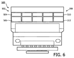
図5及び図6は、非限定的な、デュアルエネルギー(ダブルデッカー)検出器リーフ118を持つタイル500の例を示す。図5は、前記タイルの側面図であり、図6は前記タイルの正面図である。他の実施態様は、3以上のエネルギーを分解する検出器リーフを含む。一般的に、異なるシンチレーター/光センサー部分領域の対(ペア)がそれぞれの異なるエネルギー範囲で使用される。示されるデュアルエネルギー検出器リーフ118は実質的には図2から4に記載されたシングルエネルギー検出器リーフと類似するが、違いは、2つの異なるエネルギー範囲(より低い範囲と、より高い範囲)内のエネルギーを持つX線フォトンを別々に検出するための、上部の部分領域504と底部の部分領域506である2つの異なるシンチレーション部分領域を有するシンチレーターアレイ502と、対応する光学フォトンを検出するための2つの相補的な感光部分領域である第1の部分領域510及び第2の部分領域512を有する感光領域508と、を含んでいるという点である。
FIGS. 5 and 6 show an example of a
種々のシンチレーション材料がここで説明されたシンチレーターで使用され得る。例としては、限定されるものではないが、GOS、テルルで活性化されたZnSe(ZnSe:Te)、ユーロピウム(Eu)ドープヨウ化カルシウム(CaI 2 :Eu)、ヨウ化ストロンチウム(SrI2:Eu)及びヨウ化バリウム(BaI2:Eu)、Eu2+でドープされたセラミックアルカリ土類ヨウ化物、非ドープSrI2、及び/又はEu2+、Ce3+又はPr3+又はその他の活性化イオンでドープされたその他のシンチレーターが含まれる。これらのシンチレーション材料はまた、他の検出器と接続されて使用され得るものであり、例えば、出願番号11/912673(2007年10月26日出願、発明の名称「スペクトルCTのためのダブルデッカー検出器」)に記載されたもの(この内容は参照されて本明細書に援用される)、出願番号12/067942(2008年3月25日出願、発明の名称「薄い回路を用いたコンピュータトモグラフィー」)に記載されたもの(これらの内容は参照されて本明細書に援用される)、及びその他の検出器などである。
A variety of scintillation materials can be used in the scintillators described herein. Examples include, but are not limited to, GOS, telluride-activated ZnSe (ZnSe: Te), europium (Eu) Dopuyou of calcium (CaI 2: Eu), strontium iodide (SrI 2: Eu) and barium iodide (BaI 2: Eu), doped ceramic alkaline earth iodides in Eu 2+, undoped SrI 2, and / or E u 2+, Ce 3+ or Pr 3+ or other activator ion de It includes other scintillator that has been over-flops. These scintillation materials can also be used in conjunction with other detectors, for example,
図7は、CaI2:Eu702、SrI2:Eu704、BaI2:Eu706、SrBr2:Eu708及び非ドープSrI2710の発光スペクトルを、放射波長712の関数として示す。図7から、Eu2+でドープされたハロゲン化物の発光スペクトルは、スペクトルの紫外(UV)/青色部分内である。
FIG. 7 shows the emission spectra of CaI 2 : Eu702, SrI 2 : Eu704, BaI 2 : Eu706, SrBr 2 : Eu708 and
SrI2:Euは知られている最も効率的なシンチレーターのうちの1つである。その効率は100000フォトン/MeVを超え、及びそのエネルギー分解能は非常に高く(2%程度)、物理的限界に近づく。その融点は低く(538℃)、単結晶成長に非常に好適であり、その結晶構造は斜方晶系である。CaI2:Eu及びBaI2:Euはまた、非常に高い光収率を持つ。CaからBaへの方向に共有結合性が増加することの結果として、より重いアルカリ土類金属イオンを持つ組成物はより水に対して安定である。混合希土類ハロゲン化物Si(1−n)BanI2が使用され、値nは、0.05<n<0.15の範囲に調節されて、温度の特定の範囲にわたる光出力の温度係数を低減させる。 SrI 2: Eu is one of the most efficient scintillators known. Its efficiency exceeds 100,000 photons / MeV, and its energy resolution is very high (on the order of 2%), approaching the physical limit. Its melting point is low (538 ° C.), it is very suitable for single crystal growth, and its crystal structure is orthorhombic. CaI 2 : Eu and BaI 2 : Eu also have very high light yields. As a result of the increased covalent binding in the direction from Ca to Ba, compositions with heavier alkaline earth metal ions are more stable to water. Mixed rare earth halides Si (1-n) Ba n I 2 are used and the value n is adjusted in the range of 0.05 <n <0.15 to give a temperature coefficient of light output over a specific range of temperatures. Reduce.
前記シンチレーション材料は、湿度及び酸素を除去して粉末ハロゲン化物を物理的に混合し、前記混合物を石英アンプルに入れ、脱気して密閉した後、その融点から温度150から50℃低い温度で加熱することで製造され得る。又は、その炭酸塩を対応するハロゲン化酸と、生成物の融点よりも150から50℃低い温度で反応させることが可能である。他の技術もまたここに含まれる。CaI2、SrI2及びBaI2の単結晶は、ブリッジマン(Bridgman)法により容易に成長させることができる。これは、最適な光収率が必要とされる場合に必要である。この方法では、温度勾配が使用される。前記温度勾配は、成長する単結晶の溶融温度に等しい温度であるオーブン中の位置で大きい。単結晶はまた、チョクラルスキー(Czochralski)法により成長させることができる。 The scintillation material removes humidity and oxygen, physically mixes the powder halide, puts the mixture into a quartz ampule, deaerates and seals, and then heats at a temperature 150 to 50 ° C. lower than its melting point. Can be manufactured. Alternatively, the carbonate can be reacted with the corresponding halogenated acid at a temperature 150 to 50 ° C. below the melting point of the product. Other techniques are also included here. Single crystals of CaI 2 , SrI 2 and BaI 2 can be easily grown by the Bridgman method. This is necessary when an optimal light yield is required. In this method, a temperature gradient is used. The temperature gradient is greater at the location in the temperature der Luo Bun equal to the melting temperature of the single crystal growth. Single crystals can also be grown by the Czochralski method.
樹脂中に粉末化シンチレーターを混合することで形成される樹脂中のCaI2:Eu,SrI2:Eu又はBaI2:Euを含むハロゲン化物を含む複合体シンチレーターでは、結晶成長は必要とされない。CaI2、SrI2、BaI2又は化学的に混合された粉末中のEu2+活性化剤の均一分布を保証することは容易である。かかる複合体は、散乱や光吸収による光損失を示すが、かかる損失は、現在使用されるシンチレーターと比較してこれらのシンチレーターの非常に高い光収率により十分相殺して余りあるものである。さらに、前記複合体は、単結晶を望ましい形状及びサイズとするための機械加工を軽減する。実際、単結晶は非常に劈開しやすく;CaI2はその六方晶系構造により不透明化する傾向が大きい。 CaI in the resin formed by mixing the powdered scintillator in the resin 2: Eu, SrI 2: Eu or BaI 2: a composite scintillator comprising a halide containing the Eu, crystal growth is not required. It is easy to ensure a uniform distribution of Eu 2+ activator in CaI 2 , SrI 2 , BaI 2 or chemically mixed powders. Such composites exhibit light loss due to scattering and light absorption, which is more than offset by the very high light yield of these scintillators compared to currently used scintillators. Furthermore, the composite reduces machining to make the single crystal the desired shape and size. In fact, single crystals are very easy to cleave; CaI 2 tends to become opaque due to its hexagonal structure.
さらに、前記複合体シンチレーターは、ドクターブレード法又は印刷などの技術で構造化することができる。さらに、CaI2:Eu、SrI2:Eu又はBaI2:Euは吸湿性であり、それらをCTで使用可能とするためにそれらの結晶を切断し構造化するためには特別の条件下で注意をして加工を実施する必要がある。前記複合体では、切断は省略され得るし、構造化するために必要な場合には、前記μ結晶子がすでに前記樹脂中に埋め込まれている場合(即ち空気及び水分から保護されている)には、加工を実施することが可能である。さらには、シンチレーター材料が水分の影響を受けやすいことの影響は、「ゲッター」のような材料を前記樹脂に添加することでさらに低減され得る。CaO又はP2O5(ともに白色材料)は水と強く反応し、前記シンチレーターμ結晶子を効果的に保護する。 Further, the composite scintillator can be structured by a technique such as a doctor blade method or printing. In addition, CaI 2 : Eu, SrI 2 : Eu or BaI 2 : Eu are hygroscopic and care must be taken under special conditions to cut and structure their crystals to make them usable in CT. It is necessary to carry out processing. In the complex, cutting can be omitted and, if necessary for structuring, if the μ crystallites are already embedded in the resin (ie protected from air and moisture). Can be processed. Furthermore, the impact of shea Nchireta material susceptible to moisture can be further reduced by the addition of materials such as "getters" to the resin. CaO or P 2 O 5 (both white materials) reacts strongly with water, effectively protecting the scintillator μ crystallites.
上で説明したように、GOS、ZnSe、ZnSe:Te、CaI2:Eu、SrI2:Eu、BaI2:Eu、SrI2などを含むシンチレーターは、シングル及びマルチエネルギー検出器を含むここで説明した検出器で使用され得る。図8及び9はSrI2系シンチレーターを持つ例を示す。図8は、セラミック又は結晶シンチレーターを用いるデュアルエネルギー(ダブルデッカー型)検出器リーフ800の側面図、及び図9は、複合シンチレーターを用いるデュアルエネルギー(ダブルデッカー)検出器リーフ900の側面図である。
As described above, GOS, ZnSe, ZnSe: Te , CaI 2: Eu, SrI 2: Eu, BaI 2: Eu, scintillator, including SrI 2 has been described herein, including single and multi-energy detector Can be used with detectors. 8 and 9 show examples having SrI 2 scintillators. FIG. 8 is a side view of a dual energy (double-decker)
図10を参照して、例として、SrI2、ZnSe及びGOSについてフォトンエネルギーの関数としてのX線吸収係数が示される。示される実施態様では、y軸1002は、X線吸収係数を単位cm−1で表し、及びx軸1004はフォトンエネルギーを単位keVで表す。最初の曲線1006は、SrI2のX線吸収係数を表し、第2の曲線1008はZnSeのX線吸収係数を表し、第3の曲線1010はGOSのX線吸収係数を表す。
Referring to FIG. 10, as an example, the X-ray absorption coefficient as a function of photon energy is shown for SrI 2 , ZnSe and GOS . The shown is the embodiment, y-
図10から、SrI2の直線X線吸収係数はZnSeのそれに30keVまで従う。30keVと50keVの間は、SrI2の前記直線X線吸収係数はZnSeと比較してずっと高く、及びまたGOSよりもこれらの比較的軟X線を吸収することができ、これはヨウ素含有トレーサーへの応答を改善し得る。より高いフォトンエネルギーでは、前記SrI2吸収は実質的にGOSよりも小さくなり、より重元素のスペクトル分解を可能にする。 From FIG. 10, the linear X-ray absorption coefficient of SrI 2 follows that of ZnSe up to 30 keV. Between 30 keV and 50 keV, the linear X-ray absorption coefficient of SrI 2 is much higher compared to ZnSe, and also can absorb these relatively soft X-rays than GOS, which leads to iodine-containing tracers Can improve the response. At higher photon energies, the SrI 2 absorption will be substantially less than GOS, allowing more heavy element spectral resolution.
従って、全体のスペクトル分解能は、ZnSeの分解能と少なくとも同じ程度良好である。患者を通過した120kVpX線については、SrI2の300ミクロン厚さは、ZnSeの1mm厚さと等価なX線吸収である。 Therefore, the overall spectral resolution is at least as good as that of ZnSe . For 120kVpX rays passing through the patient, 300 micron thick SrI 2 is a 1mm thick equivalent X-ray absorption of ZnSe.
図8を参照して、前記デュアルエネルギースペクトルCT検出器800は、放射線シールド802、上部及び底部フォトダイオード804及び806を含む検出器アレイ803、MI2:Eu(M=Ca、Sr、Ba)シンチレーション結晶を含む上部シンチレーター808を含むシンチレーターアレイ807を含む。前記結晶の高さは、シンチレーターのX線吸収に依存し、SrI2:Euについて約300ミクロンである。前記結晶は、拡散防止添加剤SiOxを含む反射白色コーティング810でコーティングされ、底部シンチレーター812は、前記反射白色コーティング810でコーティングされたGOS:Pr、Ceシンチレーション結晶を含み、及び上部及び底部シンチレーター808と812との間にアルミホイル814を設けてこれらの間の光学的混信(クロストーク)を抑制あるいは防止する。
Referring to FIG. 8, the dual energy
SrI2では、X線フルエンスの約半分を吸収するための最適厚さは僅か約0.3mmである。従って、相対的に大きな面積を持つフォトダイオードに光を効率的に伝えるためにライトパイプを使用することが望ましい。好適なライトパイプ(図8には見えない)は米国特許出願公開第2010/0220833号(2010年5月10日出願、発明の名称「スペクトルCTのための検出器アレイ」)に記載されており、この内容は参照されて本明細書に援用される。又は前記ライトパイプは、前記SrI2層の下に配置され得る。この構造は、最軟X線への感度を低減し、従って、スペクトルコントラストを低減させるがまた、そうでなければ前記SrI2を攻撃する水蒸気又は酸素の全ての方向への拡散に対する厚い固体バリアを提供することとなる。 In SrI 2, the optimum thickness to absorb about half of the X-ray fluence is only about 0.3 mm. Therefore, it is desirable to use light pipes to convey light to efficiently to the photodiode with a large area relative to. A suitable light pipe (not visible in FIG. 8) is described in US Patent Application Publication No. 2010/0220833 (filed on May 10, 2010, entitled “Detector Array for Spectral CT”). The contents of which are hereby incorporated by reference. Alternatively, the light pipe may be disposed under the SrI 2 layer. This structure reduces the sensitivity of the outermost soft X-rays, therefore, it reduces the spectral contrast Furthermore, thick solid barrier to the diffusion of all directions of the water vapor or oxygen to attack the SrI 2 otherwise Will be provided.
図9を参照して、前記デュアルエネルギースペクトルCT検出器900は、放射線シールド902と、上部及び底部フォトダイオード904及び906を含む検出器アレイ903と、透明樹脂(ハロゲン化物密度に依存する高さを持ち、SrI2では6.5mm)中にMI2:Eu(M=Ca,Sr、Ba)の大きな顆粒粉末20%(質量で)を含む上部シンチレーター908、及び透明樹脂(高さ10mm)中にGOS:Pr,Ceの大きな顆粒粉末(例えば5μmよりも大きい)を20%(質量で)を含む底部シンチレーター910を含むシンチレーターアレイ907と、前記上部及び底部シンチレーター908と910の間の光学混信を防止するための、それらの間の2つの白色反射層の間のアルミニウムホイルの不透明反射層912とを含む。前記シンチレーターが固定される側918の反対側である光センサーアレイ903の後側表面916は、白色反射性塗料や光輝金属層などの反射層を有する白色反射コーティングを含む。
Referring to FIG. 9, the dual energy
SrI2が上部シンチレーター908で、透明樹脂(エポキシ又はメルカプタン樹脂、UV硬化性であるか硬化性でない)に粉末として分散された形で複合シンチレーターとして適用される場合には、好適なフォトダイオード領域は、ライトパイプを使用するよりも、それを10から30%、例えば20%程度に希釈することで達成され得る。前記複合体はそれ自体ライトパイプを形成する。従って、0.3mmの等価SrI2高さについて、前記フォトダイオードは6.5mm高さであり得る。このことは二重に有利であり、というのはこの希釈で、前記光がまた、より高い濃度では大きな散乱を生じるであろう、1から1.5mm厚さ幅の複合体を通じて効率的に前記フォトダイオードの感度表面に誘導されるからである。
When SrI 2 is an
同様にして、前記底部シンチレーター910は、GOS複合体シンチレーターで形成され、これはまた、有利には、前記光学樹脂内に約20%濃度(質量で)で分散されるGOS粉末を含み得る。かかる検出器の要素は従って、最初GOS複合樹脂、及び次にSrI2複合樹脂を、前記2つの複合体の間に金属ホイルセパレータを持つ好適なテフロン(登録商標)金型内で、前記フォトダイオードアレイの表面上に順次キャスティングすることで製造され得る。必要とされる1.2mmよりも大きな深さでキャストし、その後に余分なものを機械的に除去して、キャピラリによって形成される余分の材料を除去することを必要とし得る。
Similarly, the
図11はイメージング方法を示す。 FIG. 11 shows an imaging method.
1102では、X線放射が、ここで説明したイメージングシステム100の放射線リーフ118の感放射線検出器により感知される。
At 1102, x-ray radiation is sensed by a radiation sensitive detector of the
1104で、前記X線が、前記感放射線検出器のシングル又はマルチエネルギーシンチレーターアレイにより、前記検出された放射線を示す光フォトンへ変換される。 In 1104, the X-rays, by single or multi-energy scintillator array of the radiation-sensitive detector, is converted into light photons indicative of the detection radiation.
1106で、前記光フォトンは、前記感放射線検出器のシングル又はマルチ光センサーを介して検出される。 At 1106, the light photons are detected via a single or multiple light sensor of the radiation sensitive detector.
1108で、前記光フォトンは、前記光センサーにより、前記検出された放射線を示す電気シグナルへ変換される。 At 1108, the light photons are converted by the light sensor into an electrical signal indicative of the detected radiation.
1110で、前記シグナルは、ここで説明したフレキシブルPCBを介して前記検出器の処理電子回路へ伝達される。ここで説明されるように、前記フレキシブルPCBが、前記光センサーと、前記シンチレーターアレイの下に設けられた放射線シールドの下に設けられる処置電子回路とを電気的に接続する。 At 1110, the signal is transmitted to the processing electronics of the detector via the flexible PCB described herein. As described herein, the flexible PCB is, with the light sensor, to electrically connect the treatment electronics that provided under the radiation shield provided below the scintillator array.
1112で、前記シグナルは、前記検出器の前記処理電子回路から前記検出器を離れてプロセッサーに送られる。 At 1112, the signal leaves the detector from the processing electronics of the detector and is sent to a processor.
1114で、前記シグナルは再構成され、前記受けた放射線を示すボリュメトリック画像データを生成する。 At 1114, the signal is reconstructed to generate volumetric image data indicative of the received radiation.
ここまで本発明は好ましい実施態様を参照して説明された。当業者は、これまでの詳細な説明を読み理解することで変更及び修正に想到するであろう。本発明は、添付の特許請求の範囲又はその均等の範囲内に含まれる全てのこのような実施態様及び変更、修正を含むことを意図するものである。 So far the present invention has been described with reference to preferred embodiments. Those skilled in the art will envision changes and modifications upon reading and understanding the preceding detailed description. The present invention is intended to embrace all such embodiments, alterations, and modifications that fall within the scope of the appended claims or their equivalents.
Claims (15)
当該検出器アレイは、少なくとも1つの検出器リーフを含み、前記検出器リーフが:
放射線を受ける上部側、底部側及び後側を少なくとも含むシンチレーターアレイと;
前記シンチレーターアレイの前記後側に光学的に結合される感光領域を含む光センサー回路基板と;
前記シンチレーターアレイの下に設けられる処理電子回路と;
前記感光領域と前記処理電子回路とを電気的に結合するフレキシブル回路基板と;
前記シンチレーターアレイと前記処理電子回路との間で、前記シンチレーターアレイの底部の下に設けられ、それにより、前記シンチレーターアレイを通り抜けた残留放射線から前記処理電子回路を遮蔽する放射線シールドと;
放射線遮蔽材料を含む支持キャリアであり、前記光センサー回路基板が当該支持キャリアに固定的に取り付けられ、当該支持キャリアが、衝突する放射線から前記光センサー回路基板を遮蔽する、支持キャリアと
を有する、
検出器アレイ。 Vertical radiation sensitive detector array:
The detector array includes at least one detector leaf, wherein the detector leaf is:
A scintillator array comprising at least a top side, a bottom side and a back side for receiving radiation;
A light sensor circuit board including a photosensitive area that is optically coupled to the rear side of the front Symbol scintillator array;
Processing electronics provided under the scintillator array;
A flexible circuit board that electrically couples the photosensitive area and the processing electronics;
A radiation shield provided between the scintillator array and the processing electronics below the bottom of the scintillator array, thereby shielding the processing electronics from residual radiation that has passed through the scintillator array ;
A support carrier comprising a radiation shielding material, the photosensor circuit board being fixedly attached to the support carrier, the support carrier having a support carrier that shields the photosensor circuit board from impinging radiation ,
Detector array.
前記光センサー回路基板がさらに、シグナル伝達領域を含み、及び前記フレキシブル回路基板がシグナル受信領域及び支持領域を含み、及び
前記フレキシブル回路基板の前記シグナル受信領域が、前記シグナル伝達領域に固定的に取り付けられ、前記フレキシブル回路基板の前記支持領域が、前記支持キャリアにより可動に支持される、検出器アレイ。 Ri detector array Der according to claim 1:
The optical sensor circuit board further includes a signal transmission area, and the flexible circuit board includes a signal reception area and a support area, and the signal reception area of the flexible circuit board is fixedly attached to the signal transmission area. A detector array wherein the support area of the flexible circuit board is movably supported by the support carrier.
前記支持キャリアに対して概して垂直に、かつ前記シンチレーターアレイの前記底部側の下方で前記底部側に対して概して平行に、前記フレキシブル回路基板の前記支持領域から延在する第1の区分と;
前記シンチレーターアレイの前記底部側へ向かって、かつ前記支持キャリアに対して概して平行に、前記第1の区分から概して垂直に延在する第2の区分と
を含み、
前記処理電子回路が前記フレキシブル回路基板の前記第1の区分の下に配置される、
検出器アレイ。 The detector array of claim 2, wherein the flexible circuit board further includes:
A first section extending from the support area of the flexible circuit board generally perpendicular to the support carrier and below the bottom side of the scintillator array and generally parallel to the bottom side;
A second section extending generally vertically from the first section toward the bottom side of the scintillator array and generally parallel to the support carrier;
The processing electronics are disposed under the first section of the flexible circuit board;
Detector array.
前記フレキシブル回路基板により担持される保持装置を含み、
前記保持装置が、当該検出器アレイを、検出器タイル内の1つ以上の他の検出器アレイに対して整列させるための、少なくとも1つのアライメント孔を含む、
検出器アレイ。 The detector array of claim 3, further comprising:
Including a holding device carried by the flexible circuit board,
The holding device includes at least one alignment hole for aligning the detector array with one or more other detector arrays in the detector tile;
Detector array.
亜鉛セレニドを含む上部シンチレーターアレイ;及び
前記上部シンチレーターアレイの下に配置され、かつガドリニウムオキシサルファイドを含む少なくとも1つの他のシンチレーターアレイ
を含む、検出器アレイ。 6. A detector array according to any one of claims 1 to 5, wherein the scintillator array:
A detector array comprising: an upper scintillator array comprising zinc selenide; and at least one other scintillator array disposed below the upper scintillator array and comprising gadolinium oxysulfide.
ハロゲン化物シンチレーション材料を含む上部シンチレーターアレイ;及び
前記上部シンチレーターアレイの下に配置され、かつガドリニウムオキシサルファイドを含む少なくとも1つの他のシンチレーターアレイ
を含む、検出器アレイ。 6. A detector array according to any one of claims 1 to 5, wherein the scintillator array:
A detector array comprising: an upper scintillator array comprising a halide scintillation material; and at least one other scintillator array disposed below the upper scintillator array and comprising gadolinium oxysulfide.
放射線を受ける上部側、底部側及び後側を少なくとも含むシンチレーターアレイと;
前記シンチレーターアレイの前記後側に光学的に結合される感光領域を含む光センサー回路基板と;
前記シンチレーターアレイの下に配置される処理電子回路と;
前記感光領域と前記処理電子回路とを電気的に結合するフレキシブル回路基板と;
前記シンチレーターアレイと前記処理電子回路との間で、前記シンチレーターアレイの底部の下に設けられ、それにより、前記シンチレーターアレイを通り抜けた残留放射線から前記処理電子回路を遮蔽する放射線シールドと;
放射線遮蔽材料を含む支持キャリアであり、前記光センサー回路基板が当該支持キャリアに固定的に取り付けられ、当該支持キャリアが、衝突する放射線から前記光センサー回路基板を遮蔽する、支持キャリアと
を有する、検出することと、
前記検出された放射線を示すシグナルを生成することと、
前記シグナルを再構成して、ボリュメトリック画像データを生成することと、
を有する方法。 Detecting radiation by at least one detector leaf of the detector array of the imaging system, the detector leaf comprising:
A scintillator array comprising at least a top side, a bottom side and a back side for receiving radiation;
A light sensor circuit board including a photosensitive area that is optically coupled to the rear side of the front Symbol scintillator array;
Processing electronics disposed under the scintillator array;
A flexible circuit board that electrically couples the photosensitive area and the processing electronics;
A radiation shield provided between the scintillator array and the processing electronics below the bottom of the scintillator array, thereby shielding the processing electronics from residual radiation that has passed through the scintillator array ;
A support carrier comprising a radiation shielding material, the photosensor circuit board being fixedly attached to the support carrier, the support carrier having a support carrier that shields the photosensor circuit board from impinging radiation , Detecting,
Generating a signal indicative of the detected radiation;
Reconstructing the signal to generate volumetric image data;
Having a method.
Applications Claiming Priority (3)
| Application Number | Priority Date | Filing Date | Title |
|---|---|---|---|
| US201161439077P | 2011-02-03 | 2011-02-03 | |
| US61/439,077 | 2011-02-03 | ||
| PCT/IB2012/050426 WO2012104775A2 (en) | 2011-02-03 | 2012-01-30 | Single or multi-energy vertical radiation sensitive detectors |
Publications (3)
| Publication Number | Publication Date |
|---|---|
| JP2014510902A JP2014510902A (en) | 2014-05-01 |
| JP2014510902A5 JP2014510902A5 (en) | 2015-07-30 |
| JP6010051B2 true JP6010051B2 (en) | 2016-10-19 |
Family
ID=45571578
Family Applications (1)
| Application Number | Title | Priority Date | Filing Date |
|---|---|---|---|
| JP2013552300A Active JP6010051B2 (en) | 2011-02-03 | 2012-01-30 | Single or multi energy vertical radiation sensitive detector array and radiation detection method |
Country Status (7)
| Country | Link |
|---|---|
| US (1) | US9140808B2 (en) |
| EP (1) | EP2671097B1 (en) |
| JP (1) | JP6010051B2 (en) |
| CN (1) | CN103339527B (en) |
| BR (1) | BR112013019490A2 (en) |
| RU (1) | RU2589252C2 (en) |
| WO (1) | WO2012104775A2 (en) |
Families Citing this family (32)
| Publication number | Priority date | Publication date | Assignee | Title |
|---|---|---|---|---|
| DE102012202927B4 (en) | 2012-02-27 | 2021-06-10 | Osram Gmbh | LIGHT SOURCE WITH LED CHIP AND LUMINOUS LAYER |
| JP2015524056A (en) * | 2012-05-22 | 2015-08-20 | アナロジック コーポレイション | Sensing system and detector array coupling assembly {DETECTIONSYSTEMANDDETECTORRAYRAYTERNECTANCENECTASSEMBLIES} |
| US9748300B2 (en) | 2013-09-05 | 2017-08-29 | Koninklijke Philips N.V. | Radiation detector element |
| CN103549967B (en) * | 2013-09-27 | 2015-11-25 | 沈阳东软医疗系统有限公司 | A kind of detector module |
| JP6574419B2 (en) * | 2013-11-15 | 2019-09-11 | コーニンクレッカ フィリップス エヌ ヴェKoninklijke Philips N.V. | Double-sided organic photodetector on flexible substrate |
| US9257205B2 (en) * | 2013-11-26 | 2016-02-09 | General Electric Company | Radiation detector module, radiation detector and radiation imaging apparatus |
| WO2015131102A1 (en) * | 2014-02-28 | 2015-09-03 | The General Hospital Corporation | System and method for processing radiation detectors using laser beams |
| JP6529858B2 (en) * | 2014-08-20 | 2019-06-12 | キヤノンメディカルシステムズ株式会社 | X-ray CT apparatus and X-ray detector |
| US9337233B1 (en) | 2014-12-15 | 2016-05-10 | General Electric Company | Photodiode array for imaging applications |
| CN107646091B (en) * | 2015-04-14 | 2019-11-15 | 模拟技术公司 | Detector array for radiating system |
| US11156727B2 (en) * | 2015-10-02 | 2021-10-26 | Varian Medical Systems, Inc. | High DQE imaging device |
| US9980697B2 (en) * | 2015-12-28 | 2018-05-29 | L-3 Communications Security & Detection Systems, Inc. | Reference detector for correcting fluctuations in dose and energy of x-ray sources |
| US10162065B2 (en) * | 2016-01-29 | 2018-12-25 | Vanderbilt University | Gamma ray spectroscope for determining a composition of an asteroid or the regolith of the asteroid |
| WO2017179609A1 (en) * | 2016-04-15 | 2017-10-19 | 株式会社小糸製作所 | Nanocomposite and nanocomposite production method |
| US10192646B2 (en) * | 2016-04-25 | 2019-01-29 | General Electric Company | Radiation shielding system |
| JP6776024B2 (en) * | 2016-06-30 | 2020-10-28 | キヤノンメディカルシステムズ株式会社 | X-ray detector, X-ray detector module, support member and X-ray CT device |
| WO2018077681A1 (en) * | 2016-10-26 | 2018-05-03 | Koninklijke Philips N.V. | Radiation detector scintillator with an integral through-hole interconnect |
| KR102563942B1 (en) | 2016-11-30 | 2023-08-04 | 더 리서치 파운데이션 포 더 스테이트 유니버시티 오브 뉴욕 | Hybrid Active Matrix Flat Panel Detector System and Method |
| CN106483153A (en) * | 2016-12-23 | 2017-03-08 | 同方威视技术股份有限公司 | Dual-energy detector and radiation checking system |
| JP7062362B2 (en) * | 2017-01-18 | 2022-05-06 | キヤノン・コンポーネンツ株式会社 | Radiation detector and radiation detector |
| JP7023605B2 (en) | 2017-01-18 | 2022-02-22 | キヤノン・コンポーネンツ株式会社 | Radiation detector and radiation detector |
| EP3619553A1 (en) * | 2017-05-01 | 2020-03-11 | Koninklijke Philips N.V. | Multi-layer radiation detector |
| US10261213B2 (en) * | 2017-06-07 | 2019-04-16 | General Electric Company | Apparatus and method for flexible gamma ray detectors |
| KR20200083433A (en) | 2017-08-03 | 2020-07-08 | 더 리서치 파운데이션 포 더 스테이트 유니버시티 오브 뉴욕 | Dual-screen digital radiography with asymmetric reflective screen |
| US11181488B2 (en) * | 2017-08-31 | 2021-11-23 | Koninklijke Philips N.V. | Multi-layer detector with a monolithic scintillator |
| JP6985882B2 (en) * | 2017-10-13 | 2021-12-22 | 株式会社小糸製作所 | Scintillator material and radiation detector |
| JP7058998B2 (en) * | 2017-12-22 | 2022-04-25 | キヤノンメディカルシステムズ株式会社 | Detector module and X-ray CT device |
| CN110441811B (en) * | 2019-08-20 | 2021-05-04 | 上海联影医疗科技股份有限公司 | PET detector and medical imaging equipment with same |
| US11762108B2 (en) * | 2020-01-21 | 2023-09-19 | LightSpin Technologies Inc. | Modular pet detector comprising a plurality of modular one-dimensional arrays of monolithic detector sub-modules |
| CN116904183A (en) * | 2020-09-30 | 2023-10-20 | 株式会社博迈立铖 | Scintillator structure and method for manufacturing same |
| US11740367B2 (en) | 2022-01-07 | 2023-08-29 | Analogic Corporation | Radiation detectors for scanning systems, and related scanning systems |
| US12013503B2 (en) * | 2022-10-07 | 2024-06-18 | Cintilight, Llc | Lateral crystal photodiode readouts and switched diode networks for processing nuclear events |
Family Cites Families (28)
| Publication number | Priority date | Publication date | Assignee | Title |
|---|---|---|---|---|
| EP1051641A1 (en) * | 1998-10-28 | 2000-11-15 | Koninklijke Philips Electronics N.V. | Computer tomograph detector |
| JP4532782B2 (en) | 2000-07-04 | 2010-08-25 | キヤノン株式会社 | Radiation imaging apparatus and system |
| JP3598957B2 (en) | 2000-09-12 | 2004-12-08 | ソニー株式会社 | Printhead manufacturing method |
| JP3840050B2 (en) * | 2000-11-01 | 2006-11-01 | キヤノン株式会社 | Electromagnetic wave converter |
| JP2002148342A (en) * | 2000-11-07 | 2002-05-22 | Canon Inc | Radiation imaging device |
| US6717150B2 (en) * | 2000-12-12 | 2004-04-06 | Ge Medical Systems Global Technology Company, Llc | Solid-state CT detector modules with improved scintillator/diode coupling |
| JP2003084066A (en) * | 2001-04-11 | 2003-03-19 | Nippon Kessho Kogaku Kk | Component for radiation detector, radiation detector, and radiation-detection unit |
| AU2002223114A1 (en) * | 2001-11-20 | 2003-06-10 | Philips Medical Systems Technologies Ltd. | Ct detector-module having radiation shielding for the processing circuitry |
| WO2003065074A1 (en) * | 2002-02-01 | 2003-08-07 | Board Of Regents, The University Of Texas System | Asymmetrically placed cross-coupled scintillation crystals |
| EP1543351A1 (en) * | 2002-09-18 | 2005-06-22 | Koninklijke Philips Electronics N.V. | X-ray detector with a plurality of detector units |
| WO2004027453A1 (en) * | 2002-09-18 | 2004-04-01 | Koninklijke Philips Electronics N.V. | Radiation detector |
| AU2003288652A1 (en) * | 2003-01-06 | 2004-07-29 | Koninklijke Philips Electronics N.V. | Radiation detector with shielded electronics for computed tomography |
| DE10332333B4 (en) * | 2003-07-16 | 2006-08-03 | Siemens Ag | detector module |
| CN1890580B (en) * | 2003-12-09 | 2010-09-01 | 皇家飞利浦电子股份有限公司 | Shielding for an X-ray detector |
| US7364620B2 (en) | 2004-10-28 | 2008-04-29 | Saint-Gobain Ceramics & Plastics, Inc. | Method of purifying alkaline-earth and alkali-earth halides for crystal growth |
| DE102005014187B4 (en) * | 2005-03-29 | 2017-02-23 | Siemens Healthcare Gmbh | Detector module, detector and computed tomography device |
| CN101166997A (en) * | 2005-04-26 | 2008-04-23 | 皇家飞利浦电子股份有限公司 | Detector array for spectral CT |
| WO2007039840A2 (en) | 2005-10-05 | 2007-04-12 | Koninklijke Philips Electronics, N.V. | Computed tomography detector using thin circuits |
| US7582879B2 (en) * | 2006-03-27 | 2009-09-01 | Analogic Corporation | Modular x-ray measurement system |
| US7504637B2 (en) | 2006-07-11 | 2009-03-17 | Aeroflex Colorado Springs Inc. | Two component photodiode detector |
| US20080131348A1 (en) | 2006-12-04 | 2008-06-05 | General Electric Company | Scintillation compositions and method of manufacture thereof |
| US7608829B2 (en) * | 2007-03-26 | 2009-10-27 | General Electric Company | Polymeric composite scintillators and method for making same |
| US7655919B1 (en) | 2007-11-09 | 2010-02-02 | Radiation Monitoring Devices, Inc. | Cesium and lithium-containing quaternary compound scintillators |
| US8580149B2 (en) | 2007-11-16 | 2013-11-12 | Lawrence Livermore National Security, Llc | Barium iodide and strontium iodide crystals and scintillators implementing the same |
| JP5032276B2 (en) | 2007-11-19 | 2012-09-26 | 株式会社東芝 | Radiation detector |
| US8431041B2 (en) * | 2008-03-31 | 2013-04-30 | Stc.Unm | Halide-based scintillator nanomaterial |
| US20100268074A1 (en) * | 2008-07-02 | 2010-10-21 | Radiation Monitoring Devices, Inc. | Strontium halide scintillators, devices and methods |
| JP5281484B2 (en) | 2009-05-28 | 2013-09-04 | 浜松ホトニクス株式会社 | Radiation detection unit |
-
2012
- 2012-01-30 JP JP2013552300A patent/JP6010051B2/en active Active
- 2012-01-30 CN CN201280007521.9A patent/CN103339527B/en active Active
- 2012-01-30 RU RU2013140544/28A patent/RU2589252C2/en not_active IP Right Cessation
- 2012-01-30 US US13/979,866 patent/US9140808B2/en active Active
- 2012-01-30 BR BR112013019490A patent/BR112013019490A2/en not_active IP Right Cessation
- 2012-01-30 WO PCT/IB2012/050426 patent/WO2012104775A2/en active Application Filing
- 2012-01-30 EP EP12703356.1A patent/EP2671097B1/en active Active
Also Published As
| Publication number | Publication date |
|---|---|
| US20130327947A1 (en) | 2013-12-12 |
| EP2671097A2 (en) | 2013-12-11 |
| RU2589252C2 (en) | 2016-07-10 |
| US9140808B2 (en) | 2015-09-22 |
| WO2012104775A9 (en) | 2013-03-07 |
| RU2013140544A (en) | 2015-03-10 |
| WO2012104775A3 (en) | 2013-01-17 |
| CN103339527B (en) | 2016-06-22 |
| WO2012104775A2 (en) | 2012-08-09 |
| BR112013019490A2 (en) | 2019-09-24 |
| EP2671097B1 (en) | 2016-10-19 |
| CN103339527A (en) | 2013-10-02 |
| JP2014510902A (en) | 2014-05-01 |
Similar Documents
| Publication | Publication Date | Title |
|---|---|---|
| JP6010051B2 (en) | Single or multi energy vertical radiation sensitive detector array and radiation detection method | |
| JP2014510902A5 (en) | ||
| US9012857B2 (en) | Multi-layer horizontal computed tomography (CT) detector array with at least one thin photosensor array layer disposed between at least two scintillator array layers | |
| JP5587788B2 (en) | Radiation sensitive detector with scintillator in composite resin | |
| US10371830B2 (en) | Radiation detector for combined detection of low-energy radiation quanta and high-energy radiation quanta | |
| CN109891269B (en) | Radiation detector scintillator with integral via interconnect | |
| RU2595795C2 (en) | Spectral image detector | |
| RU2505840C2 (en) | Spectral imaging detector | |
| US20080253507A1 (en) | Computed Tomography Detector Using Thin Circuits | |
| JP2010513908A (en) | Energy decomposition detection system and imaging system | |
| JP2001311779A (en) | X-ray detector | |
| US7211801B2 (en) | Radiation detector | |
| JP3715164B2 (en) | Medium that absorbs X-rays and reflects light for X-ray detector arrays | |
| JPH1184013A (en) | Radiation detector | |
| JP2019163970A (en) | Scintillator array, radiation detector, and radiation computer tomography apparatus | |
| CN116031271B (en) | Pseudo three-energy detector and preparation method thereof |
Legal Events
| Date | Code | Title | Description |
|---|---|---|---|
| A621 | Written request for application examination |
Free format text: JAPANESE INTERMEDIATE CODE: A621 Effective date: 20150129 |
|
| A521 | Request for written amendment filed |
Free format text: JAPANESE INTERMEDIATE CODE: A523 Effective date: 20150612 |
|
| A977 | Report on retrieval |
Free format text: JAPANESE INTERMEDIATE CODE: A971007 Effective date: 20151125 |
|
| A131 | Notification of reasons for refusal |
Free format text: JAPANESE INTERMEDIATE CODE: A131 Effective date: 20151208 |
|
| A521 | Request for written amendment filed |
Free format text: JAPANESE INTERMEDIATE CODE: A523 Effective date: 20160307 |
|
| TRDD | Decision of grant or rejection written | ||
| A01 | Written decision to grant a patent or to grant a registration (utility model) |
Free format text: JAPANESE INTERMEDIATE CODE: A01 Effective date: 20160823 |
|
| A61 | First payment of annual fees (during grant procedure) |
Free format text: JAPANESE INTERMEDIATE CODE: A61 Effective date: 20160915 |
|
| R150 | Certificate of patent or registration of utility model |
Ref document number: 6010051 Country of ref document: JP Free format text: JAPANESE INTERMEDIATE CODE: R150 |
|
| R250 | Receipt of annual fees |
Free format text: JAPANESE INTERMEDIATE CODE: R250 |
|
| R250 | Receipt of annual fees |
Free format text: JAPANESE INTERMEDIATE CODE: R250 |
|
| R250 | Receipt of annual fees |
Free format text: JAPANESE INTERMEDIATE CODE: R250 |
|
| R250 | Receipt of annual fees |
Free format text: JAPANESE INTERMEDIATE CODE: R250 |
|
| R250 | Receipt of annual fees |
Free format text: JAPANESE INTERMEDIATE CODE: R250 |