JP7062362B2 - Radiation detector and radiation detector - Google Patents
Radiation detector and radiation detector Download PDFInfo
- Publication number
- JP7062362B2 JP7062362B2 JP2017006792A JP2017006792A JP7062362B2 JP 7062362 B2 JP7062362 B2 JP 7062362B2 JP 2017006792 A JP2017006792 A JP 2017006792A JP 2017006792 A JP2017006792 A JP 2017006792A JP 7062362 B2 JP7062362 B2 JP 7062362B2
- Authority
- JP
- Japan
- Prior art keywords
- radiation
- wiring board
- shielding member
- incident
- radiation detector
- Prior art date
- Legal status (The legal status is an assumption and is not a legal conclusion. Google has not performed a legal analysis and makes no representation as to the accuracy of the status listed.)
- Active
Links
Images


Description
本発明は、放射線検出器および放射線検出装置に関する。特には、入射した放射線により蛍光を発する蛍光体とこの蛍光を光電変換する光電変換素子とを有する放射線検出器と、この放射線検出器が適用された放射線検出装置に関する。 The present invention relates to a radiation detector and a radiation detector. In particular, the present invention relates to a radiation detector having a phosphor that emits fluorescence by incident radiation and a photoelectric conversion element that photoelectrically converts the fluorescence, and a radiation detection device to which the radiation detector is applied.
従来、放射線検出器には、入射した放射線により励起して蛍光(例えば可視光)を発する蛍光体と、蛍光体が発する蛍光を電気信号に変換する(光電変換する)光電変換素子が実装されるとともに電気回路が形成される配線板とを有するものがある。このような放射線検出器において、放射線が配線板に入射するとノイズが発生することがある。このため、放射線が配線板に入射しないようにすることが好ましい。特許文献1と特許文献2には、スリット状の開口が設けられた遮蔽部材により光電変換素子および電気回路を覆う構成が開示されている。
Conventionally, a radiation detector is equipped with a phosphor that is excited by incident radiation to emit fluorescence (for example, visible light) and a photoelectric conversion element that converts the fluorescence emitted by the phosphor into an electric signal (photoelectric conversion). Some have a wiring board on which an electric circuit is formed. In such a radiation detector, noise may be generated when radiation is incident on the wiring board. Therefore, it is preferable to prevent radiation from entering the wiring board.
しかしながら、特許文献1と特許文献2に記載の構成では、放射線検出器の組み立てにおいて、遮蔽部材と電気回路とを精密に位置合わせしなければならない。例えば位置決めの精度が低いと、開口を通過した放射線が電気回路に入射してノイズが発生するおそれがある。
However, in the configurations described in
上述した実情に鑑み、本発明が解決しようとする課題は、電気回路が設けられた配線板への放射線の入射を抑制してノイズを抑制することである。 In view of the above-mentioned circumstances, the problem to be solved by the present invention is to suppress the incident of radiation on the wiring board provided with the electric circuit to suppress the noise.
前記課題を解決するため、本発明は、入射した放射線を受けて光を発する波長変換部材と、前記波長変換部材が発する前記光を電気信号に変換する光電変換部と、前記光電変換部が実装されている配線板と、前記配線板のうち前記光電変換部が配置された第1表面側と反対側の第2表面側に配置されている電子部品と、前記波長変換部材、前記光電変換部、前記配線板、前記電子部品を収容しており、且つ前記放射線の入射経路となる開口部が設けられている筐体と、を有する放射線検出器であって、前記開口部から前記筐体内に入射した放射線の前記配線板及び前記電子部品への入射量を低減する遮蔽部材を備えており、前記遮蔽部材は、前記放射線の入射方向視において前記配線板及び前記電子部品と重なるように設けられていることを特徴とする。 In order to solve the above problems, the present invention mounts a wavelength conversion member that receives incident radiation and emits light , a photoelectric conversion unit that converts the light emitted by the wavelength conversion member into an electric signal, and the photoelectric conversion unit. The wiring board , the electronic component arranged on the second surface side of the wiring board opposite to the first surface side on which the photoelectric conversion unit is arranged, the wavelength conversion member , and the photoelectric conversion unit. A radiation detector comprising the wiring plate , a housing that houses the electronic components and is provided with an opening that serves as an incident path for the radiation, from the opening into the housing. A shielding member for reducing the amount of incident light incident on the wiring plate and the electronic component is provided, and the shielding member is provided so as to overlap the wiring plate and the electronic component in the incident direction view of the radiation. It is characterized by being .
本発明によれば、放射線が配線板に入射することが抑制され、配線板においてノイズが発生することを抑制できる。 According to the present invention, radiation can be suppressed from being incident on the wiring board, and noise can be suppressed from being generated on the wiring board.
以下に、本発明の実施形態について、図面を参照して詳細に説明する。本発明の実施形態に係る放射線検出器は、所定の一側を検査対象物および放射線源に向けて使用される。そして、放射線検出器は、放射線源から曝射されて前記所定の一側に所定の方向から入射した放射線を検出して光電変換し、放射線画像信号(放射線画像データ)を生成する。説明の便宜上、各図においては放射線検出器の3次元の各方向を、X,Y,Zの各矢印で示す。X方向は放射線検出器の長尺方向であり、例えば主走査方向である。Y方向は放射線検出器の短尺方向であり、例えば副走査方向である。Z方向は上下方向(放射線の入射方向)である。なお、Z方向については、使用時において放射線源や検査対象物に向ける一側(放射線が入射する一側)を上側とし、その反対側を下側とする。そして、本発明の実施形態に係る放射線検出器は、上側から入射した放射線(光軸が上下方向に平行な放射線)を検出する。 Hereinafter, embodiments of the present invention will be described in detail with reference to the drawings. The radiation detector according to the embodiment of the present invention is used with a predetermined side facing the inspection object and the radiation source. Then, the radiation detector detects and photoelectrically converts the radiation exposed from the radiation source and incident on the predetermined side from a predetermined direction, and generates a radiation image signal (radiation image data). For convenience of explanation, each of the three-dimensional directions of the radiation detector is indicated by the X, Y, and Z arrows in each figure. The X direction is the long direction of the radiation detector, for example, the main scanning direction. The Y direction is a short direction of the radiation detector, for example, a sub-scanning direction. The Z direction is the vertical direction (the incident direction of radiation). In the Z direction, one side facing the radiation source or the object to be inspected (one side on which radiation is incident) at the time of use is the upper side, and the opposite side is the lower side. Then, the radiation detector according to the embodiment of the present invention detects radiation incident from above (radiation whose optical axis is parallel in the vertical direction).
<放射線検出器>
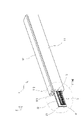
まず、放射線検出器1の構成例について、図1~図4を参照して説明する。図1は、本発明の実施形態に係る放射線検出器1の構成例を模式的に示す分解斜視図である。図2は、本発明の実施形態に係る放射線検出器1の構成例を模式的に示す外観斜視図である。図3は、図2のIII部拡大図であり、センサ基板モジュール2の構成例を模式的に示す図である。図4は、本発明の実施形態に係る放射線検出器1の構成例を模式的に示す図であり、主走査方向に直角な面で切断した断面図である。図1~図4に示すように、本発明の実施形態に係る放射線検出器1は、本体フレーム11と、センサ基板モジュール2と、波長変換部材3と、本体カバー12とを有する。
<Radiation detector>
First, a configuration example of the
本体フレーム11は、放射線検出器1の筐体である。本体フレーム11は、例えば、全体として主走査方向に長い直方体状や棒状の形状を有しており、遮光性を有する材料により一体に形成されている。遮光性を有する材料としては、例えば、黒色に着色されたポリカーボネート(PC)など、各種樹脂材料が適用できる。本体フレーム11には、センサ基板モジュール2を収容可能なセンサ基板モジュール収容部111と、放射線の経路である開口部112が設けられている。センサ基板モジュール収容部111は、例えば、主走査方向に長く、下側(放射線が入射する一側とは反対側の一側、検査対象物Qや放射線源51(図7参照)に向ける一側とは反対側の一側)が開口する溝状や凹状の部分である。開口部112は、本体フレーム11の上側(放射線が入射する一側、検査対象物Qや放射線源51に向ける一側)の表面(外周面)とセンサ基板モジュール収容部111とを連通している。この開口部112は、例えば、上下方向視において主走査方向に長い形状を有し、本体フレーム11を上下方向に貫通するスリット状の貫通孔が適用される。
The
センサ基板モジュール2は、配線板21と、この配線板21に設けられる所定の数の光電変換素子4および遮蔽部材22とを有する。
The
センサ基板モジュール2の配線板21は、長尺板状の形状を有する。配線板21には所定の配線パターンが設けられている。配線板21に設けられている配線パターンには、例えば、後述する光電変換素子4と電気的に接続するためのパッド211が含まれる。なお、配線板21の種類(材質等)は特に限定されるものではなく、従来公知の各種プリント配線板など、従来公知の各種配線板が適用できる。また、配線板21に設けられる配線パターンの具体的な構成(形状など)も特に限定されるものではなく、配線板21に実装される光電変換素子4の構成などに応じて適宜設定される。説明の便宜上、配線板21の表面のうち、光電変換素子4が実装される表面を第1の表面と称し、その反対側の面を第2の表面と称する。本発明の実施形態では、センサ基板モジュール2の配線板21は、第1の表面が主走査方向および上下方向(放射線の入射方向)に平行で、かつ長尺方向が主走査方向に平行な向きで配置される。すなわち、配線板21は、第1の表面に直角な方向視で、一方の長辺に相当する端面が上側を向く向きで配置される。
The
光電変換素子4は光電変換部の例であり、後述する波長変換部材3の蛍光層32が発する蛍光を受光する受光部42を有し、受光部42に入射した蛍光を光電変換して放射線画像信号(放射線画像データ)を生成する。本発明の実施形態では、光電変換素子4(光電変換部)として、フォトダイオードアレイが適用される例を示す。フォトダイオードアレイは、複数の受光部42(フォトダイオード)と所定の数の電極43とを有する電子部品であり、受光部42に入射した光の強度に応じた電気信号を生成する。説明の便宜上、光電変換素子4の受光部42が設けられる面を「受光面41」と称する。光電変換素子4がフォトダイオードアレイであれば、受光面41は細長い形状を有しており、複数の受光部42が受光面41の短尺方向の一側寄りに一方の長辺に平行となるように直線状(一次元状)に並べて設けられている。また、所定の数の電極43は、受光面41の短尺方向の他方の一側寄り(複数の受光部42が設けられる一側とは反対側の一側寄り)に設けられている。そして、配線板21の第1の表面には、複数の光電変換素子4(フォトダイオードアレイ)が、配線板21の長尺方向(主走査方向)に直線状(一次元状)に並べて実装されている。また、それぞれの光電変換素子4(フォトダイオードアレイ)は、複数の受光部42の配列方向が配線板21の長尺方向と平行となる向きで実装されている。さらに、光電変換素子4は、センサ基板モジュール2が本体フレーム11のセンサ基板モジュール収容部111に収容された状態で、受光部42が設けられる側が上側に位置し、電極43が設けられる側が下側に位置する向きとなるように、配線板21に実装されている。
The
なお、光電変換素子4(光電変換部)としてのフォトダイオードアレイの構成は、前記構成に限定されるものではない。それぞれのフォトダイオードアレイは、所定の方向に直線状に並べて設けられる複数の受光部42を有する構成であればよい。さらに、光電変換素子4はフォトダイオードアレイに限定されるものではない。光電変換素子4は、後述する波長変換部材3の蛍光層32が発する蛍光を電気信号に光電変換できる電子部品であればよい。例えば、光電変換素子4には、フォトダイオードやイメージセンサICなどといった、公知の各種光電変換素子が適用できる。
The configuration of the photodiode array as the photoelectric conversion element 4 (photoelectric conversion unit) is not limited to the above configuration. Each photodiode array may have a configuration having a plurality of light receiving
波長変換部材3は、放射線を光電変換素子4が光電変換可能な波長の光(本発明の実施形態では可視光)に変換する波長変換部の例である。波長変換部材3は、放射線が入射すると励起して蛍光(可視光)を発する。波長変換部材3は、基材層31と、基材層31の一方の表面に積層して設けられる蛍光層32と、蛍光層32に積層して設けられる反射層33とを有し、全体として主走査方向に長い板状やシート状の形状を有する。
The
基材層31には、透明な材料(より具体的には、蛍光層32が発する蛍光(可視光)の透過率が高い材料)の板やシートが適用される。例えば、基材層31には、ポリエチレンテレフタラート(PET)などといった、透明な樹脂材料の板やシートが適用できる。蛍光層32は、放射線が入射すると励起して蛍光(可視光)を発する材料の層である。蛍光層32には、例えば、ガドリニウムオキサイドサルファ(GOS)などといった蛍光材料が適用できる。反射層33は、蛍光層32が発する蛍光の反射率が高く放射線の透過率が高い材料からなる層である。反射層33には、例えば、アルミナや炭酸カルシウムなどといった、可視光の反射率と放射線の透過率が高い材料が適用できる。
A plate or sheet made of a transparent material (more specifically, a material having a high transmittance of fluorescence (visible light) emitted by the fluorescent layer 32) is applied to the
なお、波長変換部材3は、前記構成に限定されるものではない。波長変換部材3は、入射した放射線により励起して光電変換素子4が光電変換可能な波長の蛍光を発する蛍光層32を有していればよい。例えば、波長変換部材3の蛍光層32には、ガドリニウムオキサイドサルファのほか、ヨウ化セシウム(CSI)やアモルファスセレン(A-SE)などが適用できる。また、基材層31も、ポリエチレンテレフタラートに限定されるものではなく、各種樹脂材料やガラスなどが適用できる。反射層33も、可視光の反射率と放射線の透過率が高い材料であればよい。なお、蛍光層32が潮解性を有する材料からなる場合には、波長変換部材3は、蛍光層32の潮解を抑制するために、蛍光層32を覆う保護層を有することが好ましい。この場合、保護層には、フッ素系樹脂などといった、遮水性や撥水性の高い材料が適用される。また、波長変換部材3の寸法および形状は、配線板21に設けられる光電変換素子4の全ての受光部42を覆うことができる寸法および形状であればよい。換言すると、配線板21に設けられる光電変換素子4に重ねて配置した場合に、全ての光電変換素子4の全ての受光部42に重なる寸法および形状であればよい。
The
遮蔽部材22は、放射線の透過率が低い材料からなるか、または放射線の透過率が低い材料を含む。また、遮蔽部材22は、全体として長尺の板状やシート状や棒状の形状を有する。例えば、遮蔽部材22には、タングステンの板やシートや棒や、タングステンが充填された紙やゴムや樹脂などといった、放射線の透過率が低い材料を含む板状やシート状や棒状の部材が適用される。そして、遮蔽部材22は、その長尺方向が主走査方向に平行で、幅方向が副走査方向に平行で、厚さ方向が上で方向に平行な向きで、配線板21の上側の端面に配置される。
The shielding
遮蔽部材22の主走査方向寸法(長尺方向寸法)は、配線板21の主走査方向寸法以上であることが好ましい。遮蔽部材22の副走査方向寸法(幅)は、配線板21の副走査方向寸法(厚さ)以上であることが好ましい。配線板21の表面に配線パターンが設けられる構成であれば、遮蔽部材22の副走査方向寸法は、配線パターンの厚さを含めた配線板21の副走査方向寸法以上であることが好ましい。遮蔽部材22の上下方向寸法(厚さ)は特に限定されるものではないが、放射線を遮蔽するという機能の観点からは大きい方が好ましく、センサ基板モジュール2や放射線検出器1の小型化の観点からは小さい方が好ましい。このため、遮蔽部材22の上下方向寸法は、遮蔽部材22を上下方向に透過する放射線の透過量が所望の透過量以下となるように、遮蔽部材22における放射線の透過率や放射線源51が曝射する放射線の強度などに応じて適宜設定される。
The main scanning direction dimension (long direction dimension) of the shielding
そして、遮蔽部材22は、配線板21の上側の端面(一方の長辺に相当する端面)に設けられる。なお、遮蔽部材22が板状やシート状である場合には、複数の遮蔽部材22が上下方向に重ねて設けられる構成であってもよい。遮蔽部材22の主走査方向寸法と副走査方向寸法とが前述の通りであれば、配線板21の上側の端面の全体が遮蔽部材22で覆われる。
The shielding
センサ基板モジュール2の配線板21には、外部と電気的に接続するためのコネクタ23が設けられていてもよい。この場合、コネクタ23の構成は特に限定されるものではなく、公知の各種コネクタが適用できる。さらに、センサ基板モジュール2の配線板21には、他の素子や電子・電気部品などが実装されていてもよい。このように本発明の実施形態では、配線板21とこの配線板21に実装される光電変換素子4などによって、放射線画像を出力する電子・電気回路が形成される。
The
本体カバー12は、主走査方向に長い板状の形状を有しており、放射線の透過率が高い材料により形成されている。本体カバー12には、例えば各種樹脂材料やガラスなどが適用できる。なお、本体カバー12の具体的な構成は特に限定されるものではない。また、放射線検出器1が本体カバー12を有さない構成であってもよい。
The
(放射線検出器の組み付け構造)
ここで、放射線検出器1の組み付け構造について説明する。
(Assembly structure of radiation detector)
Here, the assembly structure of the
配線板21の第1の表面には、複数の光電変換素子4が実装される。配線板21に実装された光電変換素子4の電極43と配線板21に設けられるパッド211とは、ボンディングワイヤー24などの所定の配線によって電気的に接続される。また、配線板21の第2の表面にはコネクタ23が実装される。この他、配線板21の第1の表面と第2の表面には、光電変換素子4以外の他の素子や電子・電気部品等が実装されることがある。さらに、配線板21の上側の端面(放射線が入射する側の端面)には、遮蔽部材22が設けられる。遮蔽部材22は、例えば接着剤や両面粘着テープなどによって、配線板21の上側(放射線の入射方向の上流側)の端面に接合される。なお、遮蔽部材22は、上下方向視(放射線の入射方向視)において、配線板21の上側の端面(放射線が入射する側の端面)の全体に重なるように接合されることが好ましい。ただし、遮蔽部材22は、上下方向視において、後述する波長変換部材3とは重ならないように設けられる。遮蔽部材22が配線板21上側の端面にのみ重なる構成であれば、上下方向視において遮蔽部材22は波長変換部材3とは重ならない。また、配線板21の表面に配線パターンが設けられる構成である場合には、遮蔽部材22は、上下方向視(放射線の入射方向視)において、配線パターンにもその上側(放射線が入射する側)に重なるように接合されることが好ましい。これにより、センサ基板モジュール2が形成される。
A plurality of
そして、センサ基板モジュール2は、本体フレーム11のセンサ基板モジュール収容部111に収容されて固定される。なお、センサ基板モジュール2は、前述のとおり、配線板21の第1の表面(光電変換素子4が実装される面)が主走査方向および上下方向に平行で、かつ、遮蔽部材22が接合される端面が上側を向く向きで、本体フレーム11のセンサ基板モジュール収容部111に収容される。
Then, the
なお、センサ基板モジュール2は、上下方向視において、配線板21および配線板21に実装されている光電変換素子4が本体フレーム11の開口部112に重ならない位置(上下方向視で、開口部112の内側に入り込まない位置)に配置されることが好ましい。また、センサ基板モジュール2の本体フレーム11への固定構造は特に限定されるものではなく、接着剤を用いる構成や、本体フレーム11の一部をカシメる構成や、ネジ止めする構成など、各種の固定構造が適用できる。
The
波長変換部材3は、基材層31が設けられる側が光電変換素子4の受光面41の側を向き、反射層33が設けられる側がその反対側を向く向きで、光電変換素子4の受光面41に重ねて配置される。特に、光電変換素子4の受光面41に直角な方向視で、波長変換部材3は、全ての光電変換素子4の全ての受光部42に重なるように配置される。ただし、光電変換素子4の電極43と配線板21のパッド211とを接続するボンディングワイヤー24などの配線と干渉しないように、波長変換部材3は、光電変換素子4の電極43とは重ならない位置に配置される(図3と図4参照)。また、波長変換部材3は、上下方向視において、本体フレーム11の開口部112と重なる位置(開口部112の内側に入り込んだ位置)に配置されることが好ましい。
In the
なお、波長変換部材3と光電変換素子4の受光面41とは、接触していてもよく、接触していなくてもよい。波長変換部材3と光電変換素子4の受光面41が接触している構成としては、例えば、波長変換部材3が光電変換素子4の受光面41に接着剤などによって接合される構成が適用できる。一方、波長変換部材3が光電変換素子4の受光面41と接触していない構成としては、波長変換部材3が本体フレーム11のセンサ基板モジュール収容部111の内周面に接合される構成が適用できる。要は、波長変換部材3は、光電変換素子4の受光面41に直角な方向視で、全ての光電変換素子4の全ての受光部42に重なるように配置されていればよく、光電変換素子4の受光面41に接触していても接触していなくてもよい。ただし、光電変換素子4による蛍光の検出の感度の向上や解像度の向上を図るためには、波長変換部材3は光電変換素子4の受光部42にできるだけ接近していることが好ましく、この場合には、波長変換部材3が光電変換素子4の受光面41に接触している構成であることが好ましい。
The
本体カバー12は、本体フレーム11の上側に設けられる。本体カバー12が本体フレーム11の上側に設けられると、本体フレーム11の内部に異物が侵入することが防止される。なお、前述のとおり、放射線検出器1が本体カバー12を有さない構成であってもよい。
The
(放射線検出器の動作)
次に、放射線検出器1の動作について説明する。放射線検出器1は、放射線源51(図7参照)から曝射された放射線が入射するように、放射線源51に所定の距離をおいて対向するように配置されて使用される。そして、放射線源51と放射線検出器1との間に検査対象物Qを通過させながら、放射線源51が検査対象物Qに放射線を曝射し、放射線検出器1が検査対象物Qを透過した放射線を検出する。
(Operation of radiation detector)
Next, the operation of the
前述のとおり、上下方向視において、遮蔽部材22は波長変換部材3に重ならないから、放射線検出器1に入射した放射線は、本体フレーム11の開口部112を通過して遮蔽部材22に遮蔽されずに波長変換部材3に入射する。波長変換部材3の蛍光層32は、放射線が入射すると励起して、入射した放射線の強度に応じた蛍光(可視光)を発する。すなわち、蛍光層32により、入射した放射線は光電変換素子4で検出可能な波長の光に変換される。そして、光電変換素子4(フォトダイオードアレイ)の受光部42は、蛍光層32が発する蛍光を電気信号に変換(光電変換)する。この際、蛍光層32が発する蛍光が反射層33において反射することにより、受光部42に入射する蛍光の光量が増加する。このため、検出感度が向上する。
As described above, since the shielding
そして、光電変換素子4は、あるタイミングにおいて受光部42が光電変換して生成した電気信号を、放射線画像信号(放射線画像データ)の1ラインの信号として出力する。なお、放射線検出器1は、このような動作を継続的に実行することにより、検査対象物Qの内部情報を有する2次元の放射線画像信号(放射線画像データ)を生成して出力することができる。
Then, the
(作用)
ここで、本発明の実施形態の作用などについて説明する。図3と図4に示すように、遮蔽部材22は、配線板21の上側の端面(一方の長辺に対応する端面)に接合されている。そして、遮蔽部材22は、上下方向視において、配線板21に重なっている。このような構成であると、上側から入射した放射線は、遮蔽部材22によって、配線板21に直接的に入射しないように遮蔽される。ここで、「放射線が直接的に入射する」とは、本体フレーム11の開口部112を通過した放射線が、他の部材で反射することなくそのまま入射することをいうものとする。このような構成であると、放射線の入射により発生するノイズを抑制でき、光電変換素子4が出力する放射線画像の画質の向上を図ることができる。なお、配線板21の表面に配線パターンが設けられる場合には、遮蔽部材22は、この配線パターンにも重なっていることが好ましい。このような構成によれば、配線板21の表面に設けられている配線パターンにも、遮蔽部材22によって放射線が直接的に入射しないように遮蔽されるから、表面に設けられている配線パターンにおいてノイズが発生することを抑制できる。
(Action)
Here, the operation and the like of the embodiment of the present invention will be described. As shown in FIGS. 3 and 4, the shielding
また、本発明の実施形態においては、遮蔽部材22が配線板21に接合されている。このため、センサ基板モジュール2の本体フレーム11への組み付け精度が低い場合であっても、配線板21に直接的に放射線が入射することが抑制される。すなわち、従来構成のように、開口部が設けられた遮蔽部材が用いられる構成では、開口部を通過した放射線が配線板に直接的に入射しないようにするためには、開口部と配線板とを厳密に位置決めしなければならない。例えば、従来構成では、上下方向視(入射する放射線の方向視)で、配線板が遮蔽部材に設けられる開口部の内側に入り込んでいると、当該入り込んでいる部分に直接的に放射線が入射することになる。このため、配線板において放射線の入射によるノイズが発生する。一方、配線板と開口部との上下方向視の距離が大きくなると、配線板に放射線が直接的に入射することは抑制できるが、蛍光部材の蛍光層と配線板に実装されている光電変換素子との距離が大きくなる。このためこの場合には、光電変換素子による蛍光の検出感度が低下するほか、出力される放射線画像の解像度が低下する。
Further, in the embodiment of the present invention, the shielding
これに対して、本発明の実施形態においては、遮蔽部材22が配線板21の上側の端面に接合されている。このような構成であると、配線板21と遮蔽部材22との位置関係は、センサ基板モジュール2の本体フレーム11への組み付け精度の影響を受けない。このため、センサ基板モジュール2の本体フレーム11への組み付け精度が低い場合であっても、放射線が直接的に配線板21に入射することが抑制される。したがって、配線板21において放射線の入射に起因するノイズの発生を抑制できる。
On the other hand, in the embodiment of the present invention, the shielding
また、波長変換部材3が光電変換素子4の受光面41に接合される構成であってもよい。このような構成であれば、光電変換素子4と波長変換部材3と遮蔽部材22との位置関係は、センサ基板モジュール2の本体フレーム11への組み付け精度に係わらず一定となる。このため、蛍光層32のうちの放射線が入射して蛍光を発する箇所と光電変換素子4の受光部42との距離も一定となるから、光電変換素子4による蛍光の検出感度の低下を抑制できるとともに、出力される放射線画像の解像度の低下を抑制できる。さらに、このような構成であると、センサ基板モジュール2の組み付け精度に個体差があっても、検出感度や解像度の個体差を抑制できる。したがって、放射線検出器1の品質の安定化を図ることができる。
Further, the
(遮蔽部材の変形例)
次に、遮蔽部材22の変形例について説明する。図5と図6は、変形例に係る遮蔽部材22が適用された放射線検出器1の構成例を模式的に示す断面図であり、図4に対応する図である。
(Modification example of shielding member)
Next, a modification of the shielding
図5は、遮蔽部材22が配線板21の表面からその略直角方向に延出している例を示す。説明の便宜上、第1の表面の側に延出している部分を「第1の延出部221」と称し、第2の表面の側に延出している部分を「第2の延出部222」と称する。
FIG. 5 shows an example in which the shielding
第1の延出部221は、上下方向視において、配線板21の第1の表面に実装されている光電変換素子4に重なっている。上下方向視において、光電変換素子4の少なくとも一部に第1の延出部221が重なっている構成であると、遮蔽部材22の第1の延出部221によって、光電変換素子4に直接的に入射する放射線の量を減少させることができる。したがって、光電変換素子4において放射線の入射によるノイズの発生を抑制できる。特に、配線板21の光電変換素子4が実装される面に直角な方向を厚さ方向とすると、第1の延出部221の厚さ方向の延出寸法B1が光電変換素子4の厚さ以上であり、上下方向視において、光電変換素子4の全体に第1の延出部221が重なっていることが好ましい。このような構成であると、光電変換素子4に上側から直接的に入射する放射線をなくすことができる。したがって、光電変換素子4におけるノイズの発生の抑制の効果を高めることができる。
The first extending portion 221 overlaps with the
一方、第1の延出部221は、上下方向視(放射線の入射方向視)において、波長変換部材3の上側(放射線が入射する側)に重なっていないことが好ましい。このような構成であると、波長変換部材3に直接的に入射する放射線が遮蔽されないから、波長変換部材3に入射する放射線の量の減少を抑制でき、放射線検出器1による放射線の検出感度を維持できる。この場合、第1の延出部221の厚さ方向寸法の延出寸法B1は、光電変換素子4の厚さと同じであればよい。なお、光電変換素子4と波長変換部材3との間に隙間が存在する場合には、第1の延出部221の厚さ方向寸法の延出寸法B1は、光電変換素子4の厚さ以上で、光電変換素子4の厚さと隙間の寸法の合計値以下であればよい。このような構成であれば、上下方向視において、遮蔽部材22は波長変換部材3と重ならない。このため、開口部112から入射した放射線は、遮蔽部材22に遮蔽されることなく波長変換部材3に到達する。ただし、第1の延出部221は、波長変換部材3の一部に重なっていてもよい。波長変換部材3の一部に第1の延出部221が重なっていても、重なっていない他の部分には上側から直接的に放射線が入射する。したがって、このような構成とすることにより、波長変換部材3の少なくとも一部には上側から直接的に放射線が入射するようにできるから、放射線検出器1による放射線の検出感度を確保することができる。
On the other hand, it is preferable that the first extending portion 221 does not overlap the upper side (the side where the radiation is incident) of the
第2の延出部222は、上下方向視において、配線板21の第2の表面に実装されている素子や電子・電気部品などに重なっている。この場合、第2の延出部222の厚さ方向の延出寸法B2は、配線板21の第2の表面に実装されている素子や電子・電気部品等の厚さ以上であることが好ましい。このような構成によれば、第2の延出部222によって、配線板21の第2の表面に実装されている素子や電子・電気部品などに上側から放射線が直接的に入射しないように遮蔽される。したがって、配線板21の第2の表面に実装されている素子や電子・電気部品などにおいてノイズが発生することを抑制できる。なお、遮蔽部材22が第2の延出部222を有すると、配線板21の第2の表面に素子や電子・電気部品などが実装されていない場合であっても、配線板21に設けられる配線パターンに放射線が入射しないように遮蔽する効果を高めることができる。したがって、配線板21に設けられている配線パターンにおいてノイズが発生することが抑制される。
The second extending portion 222 overlaps with an element, an electronic / electrical component, or the like mounted on the second surface of the
なお、図5においては、遮蔽部材22が、第1の延出部221と第2の延出部222の両方を有している構成を例に示しているが、このような構成に限定されるものではない。例えば、遮蔽部材22が第1の延出部221と第2の延出部222のいずれか一方のみを有する構成であってもよい。
Note that FIG. 5 shows an example in which the shielding
図6は、遮蔽部材22が、配線板21の上側の端面のみならず、第1の表面と第2の表面にも設けられる構成の例を示す。このような構成によれば、配線板21の第1の表面と第2の表面とは、遮蔽部材22により覆われるから、上側から入射した放射線が直接的に配線板21に入射しないように遮蔽されるのみならず、他の部材などで反射した放射線(すなわち、進行方向が上下方向に平行でない放射線)の入射も抑制できる。したがって、このような構成によれば、配線板21への放射線の入射を抑制する効果を高めることができる。
FIG. 6 shows an example of a configuration in which the shielding
さらに、このような構成においては、光電変換素子4の上側にも遮蔽部材22が設けられることになる。したがって、遮蔽部材22のうちの配線板21の第1の表面に設けられる部分は、上下方向視において光電変換素子4に重なることになるから、光電変換素子4に放射線が直接的に入射することが抑制される。したがって、光電変換素子4において、放射線の入射によるノイズの発生を抑制できる。この場合、遮蔽部材22のうちの第1の表面に設けられる部分の厚さは、前述した第1の延出部221の副走査方向の延出寸法B1と同じ寸法が適用できる。このような寸法とすることにより、遮蔽部材22が第1の延出部221を有する場合と同様の効果を奏することができる。
Further, in such a configuration, the shielding
また、配線板21の第2の表面に素子や電子・電気部品が実装される場合には、配線板21の第2の表面に遮蔽部材22が設けられると、遮蔽部材22によってこれらの素子や電子・電気部品に放射線が入射しないように遮蔽される。したがって、第2の表面に実装される素子や電子・電気部品において、放射線の入射によるノイズの発生を抑制できる。この場合、配線板21の第2の表面に実装されている素子や電子・電気部品を覆うように、遮蔽部材22が貼り付けられる構成であってもよく、上下方向視において重なる構成であってもよい。上下方向視において重なるように設けられる場合には、遮蔽部材22のうちの第2の表面に設けられる部分の厚さは、前述した第2の延出部222の副走査方向の延出寸法B2と同じ寸法が適用できる。
Further, when an element or an electronic / electrical component is mounted on the second surface of the
なお、図6においては、一体の遮蔽部材22が配線板21の第1の表面と上側の端面と第2の表面とに跨るように設けられる構成を示すが、遮蔽部材22の構成はこのような構成に限定されない。例えば、配線板21の第1の表面と上側の端面と第2の表面のそれぞれに、別体の遮蔽部材22がそれぞれ接合される構成であってもよい。また、遮蔽部材22の厚さは、配線板21の第1の表面と上側の端面と第2の表面に設けられる部分とで互いに異なっていてもよい。さらに、遮蔽部材22は、配線板21の第1の表面と第2の表面の両面に設けられる構成でなくてもよく、上側の端面に加えて、第1の表面と第2の表面のいずれか一方にのみ設けられる構成であってもよい。
Note that FIG. 6 shows a configuration in which the integrated shielding
<放射線検出装置>
次に、放射線検出装置5の構成例について、図7を参照して説明する。図7は、放射線検出装置5の構成例を模式的に示す断面図である。放射線検出装置5は、放射線源51と、本発明の実施形態に係る放射線検出器1とを有する。放射線源51には、主走査方向に長い線状の放射線を曝射することができる放射線源が適用される。なお、放射線源51は、線状の放射線を曝射できる構成であればよく、具体的な構成は限定されない。そして、放射線源51と放射線検出器1とは、検査対象物Qの搬送経路Pを挟んで対向して配置される。放射線源51が曝射した放射線は、搬送経路Pを搬送される検査対象物Qを透過して、放射線検出器1に入射する。そして、放射線検出器1は、前述の動作によって、検査対象物Qの内部情報を有する2次元の放射線画像信号(放射線画像データ)を生成して出力する。
<Radiation detection device>
Next, a configuration example of the
以上、本発明の実施形態について詳細に説明したが、前述の実施形態は、本発明を実施するにあたっての具体例を示したに過ぎない。本発明の技術的範囲は、前述の実施形態に限定されるものではない。本発明は、その趣旨を逸脱しない範囲において、種々の変更が可能である。 Although the embodiments of the present invention have been described in detail above, the above-described embodiments merely show specific examples for carrying out the present invention. The technical scope of the present invention is not limited to the above-described embodiment. The present invention can be modified in various ways without departing from the spirit of the present invention.
例えば、前述した実施形態では、光電変換素子にフォトダイオードアレイが適用される構成を示したが、光電変換素子はフォトダイオードアレイに限定されない。光電変換素子は、蛍光層が発する蛍光(可視光)を光電変換できるものであればよい。 For example, in the above-described embodiment, the photodiode array is applied to the photoelectric conversion element, but the photoelectric conversion element is not limited to the photodiode array. The photoelectric conversion element may be any as long as it can photoelectrically convert the fluorescence (visible light) emitted by the fluorescent layer.
本発明は、蛍光層および蛍光層が発する蛍光を光電変換する光電変換素子を有する放射線検出器と、この放射線検出器を有する放射線検出装置に有効に利用できるものである。そして、本発明によれば、放射線の入射に起因して生じるノイズを抑制することができる。 The present invention can be effectively used for a radiation detector having a fluorescent layer and a photoelectric conversion element that photoelectrically converts the fluorescence emitted by the fluorescent layer, and a radiation detector having the radiation detector. Then, according to the present invention, it is possible to suppress noise caused by the incident of radiation.
1:放射線検出器、11:本体フレーム、111:センサ基板モジュール収容部、112:開口部、12:本体カバー、2:センサ基板モジュール、21:配線板、211:パッド、22:遮蔽部材、221:第1の延出部、222:第2の延出部、23:コネクタ、24:ボンディングワイヤー、3:波長変換部材、31:基材層、32:蛍光層、33:反射層、4:光電変換素子、41:受光面、42:受光部、43:電極、5:放射線検出装置、51:放射線源、Q:検査対象物、P:搬送経路 1: Radiation detector, 11: Main body frame, 111: Sensor board module housing, 112: Opening, 12: Main body cover 2: Sensor board module, 21: Wiring board, 211: Pad, 22: Shielding member, 221 : 1st extension part 222: 2nd extension part, 23: connector, 24: bonding wire, 3: wavelength conversion member, 31: base material layer, 32: fluorescent layer, 33: reflective layer, 4: Photoelectric conversion element, 41: light receiving surface, 42: light receiving part, 43: electrode, 5: radiation detection device, 51: radiation source, Q: inspection object, P: transport path
Claims (17)
前記波長変換部材が発する前記光を電気信号に変換する光電変換部と、
前記光電変換部が実装されている配線板と、
前記配線板のうち前記光電変換部が配置された第1表面側と反対側の第2表面側に配置されている電子部品と、
前記波長変換部材、前記光電変換部、前記配線板、前記電子部品を収容しており、且つ前記放射線の入射経路となる開口部が設けられている筐体と、
を有する放射線検出器であって、
前記開口部から前記筐体内に入射した放射線の前記配線板及び前記電子部品への入射量を低減する遮蔽部材を備えており、
前記遮蔽部材は、前記放射線の入射方向視において前記配線板及び前記電子部品と重なるように設けられていることを特徴とする放射線検出器。 A wavelength conversion member that receives incident radiation and emits light,
A photoelectric conversion unit that converts the light emitted by the wavelength conversion member into an electric signal, and
The wiring board on which the photoelectric conversion unit is mounted and
Among the wiring boards, electronic components arranged on the second surface side opposite to the first surface side on which the photoelectric conversion unit is arranged, and
A housing that houses the wavelength conversion member, the photoelectric conversion unit, the wiring board, and the electronic components, and is provided with an opening that serves as an incident path for the radiation.
It is a radiation detector with
A shielding member for reducing the amount of radiation incident on the wiring board and the electronic component from the opening to the inside of the housing is provided.
The radiation detector is characterized in that the shielding member is provided so as to overlap with the wiring board and the electronic component in the incident direction view of the radiation.
ことを特徴とする請求項1に記載の放射線検出器。 The radiation detector according to claim 1, wherein the shielding member is configured to surround only a part of the wiring board in all directions excluding the opening.
ことを特徴とする請求項1又は2に記載の放射線検出器。 The radiation detector according to claim 1 or 2, wherein the shielding member is arranged on a line segment connecting the opening and the wiring board.
ことを特徴とする請求項1乃至3いずれか1項に記載の放射線検出器。 The radiation detector according to any one of claims 1 to 3, wherein the shielding member is arranged so as to cover the side surface of the wiring board on the side close to the opening.
ことを特徴とする請求項1乃至4いずれか1項に記載の放射線検出器。 The radiation detector according to any one of claims 1 to 4, wherein the shielding member is joined to one surface of the wiring board.
ことを特徴とする請求項1乃至5いずれか1項に記載の放射線検出器。 Any of claims 1 to 5, wherein the wavelength conversion member is not arranged on the line segment connecting the opening and a part of the wiring board, and the shielding member is arranged. The radiation detector according to item 1.
前記配線板の第1表面側に配置された放射線検出部と、
前記配線板の前記第1表面側と反対側の第2表面側に配置されている電子部品と、
入射した放射線を遮蔽する遮蔽部材と、
を有する放射線検出器であって、
前記配線板は、前記放射線の入射方向に沿って設けられており、
前記遮蔽部材は、
放射線の入射方向視において前記配線板及び前記電子部品と重なるように、且つ前記配線板及び前記電子部品への前記放射線の入射量を低減するように設けられていることを特徴とする放射線検出器。 Wiring board and
A radiation detection unit arranged on the first surface side of the wiring board,
Electronic components arranged on the second surface side opposite to the first surface side of the wiring board, and
A shielding member that shields incident radiation and
It is a radiation detector with
The wiring board is provided along the incident direction of the radiation, and is provided.
The shielding member is
A radiation detector characterized in that it is provided so as to overlap with the wiring board and the electronic component in the incident direction view of radiation and to reduce the amount of the radiation incident on the wiring board and the electronic component. ..
前記配線板の第1表面側に配置されており、入射した放射線を受けて光を発する波長変換部材と、
前記波長変換部材が発する前記光を電気信号に変換する光電変換部と、
前記配線板の前記第1表面側と反対側の第2表面側に配置されている電子部品と、
入射した放射線を遮蔽する遮蔽部材と、
を有する放射線検出器であって、
前記配線板は、前記放射線の入射方向に沿って設けられており、
前記遮蔽部材は、
放射線の入射方向視において前記配線板及び前記電子部品と重なるように、且つ前記配線板及び前記電子部品への前記放射線の入射量を低減するように設けられていることを特徴とする放射線検出器。 Wiring board and
A wavelength conversion member arranged on the first surface side of the wiring board and emitting light by receiving incident radiation, and
A photoelectric conversion unit that converts the light emitted by the wavelength conversion member into an electric signal, and
Electronic components arranged on the second surface side opposite to the first surface side of the wiring board, and
A shielding member that shields incident radiation and
It is a radiation detector with
The wiring board is provided along the incident direction of the radiation, and is provided.
The shielding member is
A radiation detector characterized in that it is provided so as to overlap with the wiring board and the electronic component in the incident direction view of radiation and to reduce the amount of the radiation incident on the wiring board and the electronic component. ..
前記遮蔽部材は、放射線の入射方向視において、前記波長変換部と重ならないように配置されていることを特徴とする請求項7に記載の放射線検出器。 It has a wavelength converter that emits light when radiation is incident on it.
The radiation detector according to claim 7, wherein the shielding member is arranged so as not to overlap with the wavelength conversion unit in the incident direction view of radiation.
前記配線板の前記第1表面に直角な方向を厚さ方向としたときの前記第1の延出部の厚さ方向寸法は、前記光電変換部の厚さ方向寸法以上であることを特徴とする請求項1乃至6、8のいずれか1項に記載の放射線検出器。 The shielding member has a first extending portion extending toward the first surface side of the wiring board.
The thickness direction dimension of the first extending portion when the direction perpendicular to the first surface of the wiring board is defined as the thickness direction is characterized in that the thickness direction dimension of the first extending portion is equal to or larger than the thickness direction dimension of the photoelectric conversion portion. The radiation detector according to any one of claims 1 to 6 and 8.
前記放射線源が曝射した放射線を検出する、請求項1乃至16いずれか1項に記載の放射線検出器と、を有することを特徴とする放射線検出装置。 Radiation source and
The radiation detection device according to claim 1, further comprising the radiation detector according to any one of claims 1 to 16, which detects the radiation exposed by the radiation source.
Priority Applications (1)
| Application Number | Priority Date | Filing Date | Title |
|---|---|---|---|
| JP2017006792A JP7062362B2 (en) | 2017-01-18 | 2017-01-18 | Radiation detector and radiation detector |
Applications Claiming Priority (1)
| Application Number | Priority Date | Filing Date | Title |
|---|---|---|---|
| JP2017006792A JP7062362B2 (en) | 2017-01-18 | 2017-01-18 | Radiation detector and radiation detector |
Publications (3)
| Publication Number | Publication Date |
|---|---|
| JP2018115955A JP2018115955A (en) | 2018-07-26 |
| JP2018115955A5 JP2018115955A5 (en) | 2020-07-09 |
| JP7062362B2 true JP7062362B2 (en) | 2022-05-06 |
Family
ID=62985323
Family Applications (1)
| Application Number | Title | Priority Date | Filing Date |
|---|---|---|---|
| JP2017006792A Active JP7062362B2 (en) | 2017-01-18 | 2017-01-18 | Radiation detector and radiation detector |
Country Status (1)
| Country | Link |
|---|---|
| JP (1) | JP7062362B2 (en) |
Cited By (1)
| Publication number | Priority date | Publication date | Assignee | Title |
|---|---|---|---|---|
| KR20110062354A (en) * | 2009-12-03 | 2011-06-10 | 웅진코웨이주식회사 | Toilet bowl |
Citations (4)
| Publication number | Priority date | Publication date | Assignee | Title |
|---|---|---|---|---|
| US20020054659A1 (en) | 2000-08-14 | 2002-05-09 | Miwa Okumura | Radiation detector, radiation detecting system and X-ray CT apparatus |
| JP2003172782A (en) | 2001-12-06 | 2003-06-20 | Hamamatsu Photonics Kk | Radiogram imaging device and its manufacturing method |
| US20120093283A1 (en) | 2010-10-15 | 2012-04-19 | Zhiqiang Liu | Method for placing a/d converter, front-lit detector and ct apparatus |
| US20130327947A1 (en) | 2011-02-03 | 2013-12-12 | Koninklijke Philips N.V. | Single or multi-energy vertical radiation sensitive detectors |
-
2017
- 2017-01-18 JP JP2017006792A patent/JP7062362B2/en active Active
Patent Citations (7)
| Publication number | Priority date | Publication date | Assignee | Title |
|---|---|---|---|---|
| US20020054659A1 (en) | 2000-08-14 | 2002-05-09 | Miwa Okumura | Radiation detector, radiation detecting system and X-ray CT apparatus |
| JP2008286800A (en) | 2000-08-14 | 2008-11-27 | Toshiba Corp | Radiation detector, radiation detection system, and x-ray ct apparatus having radiation detector |
| JP2003172782A (en) | 2001-12-06 | 2003-06-20 | Hamamatsu Photonics Kk | Radiogram imaging device and its manufacturing method |
| US20120093283A1 (en) | 2010-10-15 | 2012-04-19 | Zhiqiang Liu | Method for placing a/d converter, front-lit detector and ct apparatus |
| JP2012088301A (en) | 2010-10-15 | 2012-05-10 | Ge Medical Systems Global Technology Co Llc | Front irradiation detector, method for mounting a/d converter, and ct apparatus |
| US20130327947A1 (en) | 2011-02-03 | 2013-12-12 | Koninklijke Philips N.V. | Single or multi-energy vertical radiation sensitive detectors |
| JP2014510902A (en) | 2011-02-03 | 2014-05-01 | コーニンクレッカ フィリップス エヌ ヴェ | Single or multi-energy radiation sensitive vertical detector |
Cited By (2)
| Publication number | Priority date | Publication date | Assignee | Title |
|---|---|---|---|---|
| KR20110062354A (en) * | 2009-12-03 | 2011-06-10 | 웅진코웨이주식회사 | Toilet bowl |
| KR101685952B1 (en) * | 2009-12-03 | 2016-12-13 | 코웨이 주식회사 | Toilet bowl |
Also Published As
| Publication number | Publication date |
|---|---|
| JP2018115955A (en) | 2018-07-26 |
Similar Documents
| Publication | Publication Date | Title |
|---|---|---|
| TWI539789B (en) | Image sensor unit, image reading apparatus, and image forming apparatus | |
| JP5124226B2 (en) | Radiation detector | |
| JP2018141781A (en) | Radiation detector and radiation detection device | |
| US11693130B2 (en) | Radiation detection device | |
| WO2006049112A1 (en) | Image reading device | |
| JP5124227B2 (en) | Radiation detector | |
| JP7062362B2 (en) | Radiation detector and radiation detector | |
| US20180067047A1 (en) | Radiation detector | |
| JP7023605B2 (en) | Radiation detector and radiation detector | |
| US20180246228A1 (en) | Radiation detector and radiation detection apparatus | |
| JP6718832B2 (en) | Radiation detector and radiation detection device | |
| JP2020041935A (en) | Toner deposition amount sensor | |
| JP2007059657A (en) | Photo interrupter | |
| US20150369926A1 (en) | Radiographic photographing apparatus and radiographic photographing system | |
| JP2008277488A (en) | Light-emitting/receiving module | |
| US11774606B2 (en) | Electromagnetic wave detector, electromagnetic wave detection apparatus, inspection apparatus, and circuit board | |
| JP2018080989A (en) | Radiation detector and radiation detection device | |
| JP5551752B2 (en) | Radiation detector | |
| JP5513582B2 (en) | Radiation detector | |
| US20220313193A1 (en) | Radiation imaging apparatus and radiation imaging system | |
| JP2006147944A (en) | Photo interrupter | |
| JP5917579B2 (en) | Image sensor unit and image reading apparatus | |
| JP2558471B2 (en) | Reader | |
| JP2013254914A (en) | Position detector | |
| JP5874417B2 (en) | Image sensor |
Legal Events
| Date | Code | Title | Description |
|---|---|---|---|
| A621 | Written request for application examination |
Free format text: JAPANESE INTERMEDIATE CODE: A621 Effective date: 20200116 |
|
| A521 | Request for written amendment filed |
Free format text: JAPANESE INTERMEDIATE CODE: A523 Effective date: 20200521 |
|
| A977 | Report on retrieval |
Free format text: JAPANESE INTERMEDIATE CODE: A971007 Effective date: 20210121 |
|
| A131 | Notification of reasons for refusal |
Free format text: JAPANESE INTERMEDIATE CODE: A131 Effective date: 20210202 |
|
| A521 | Request for written amendment filed |
Free format text: JAPANESE INTERMEDIATE CODE: A523 Effective date: 20210405 |
|
| A131 | Notification of reasons for refusal |
Free format text: JAPANESE INTERMEDIATE CODE: A131 Effective date: 20211005 |
|
| A521 | Request for written amendment filed |
Free format text: JAPANESE INTERMEDIATE CODE: A523 Effective date: 20211115 |
|
| TRDD | Decision of grant or rejection written | ||
| A01 | Written decision to grant a patent or to grant a registration (utility model) |
Free format text: JAPANESE INTERMEDIATE CODE: A01 Effective date: 20220322 |
|
| A61 | First payment of annual fees (during grant procedure) |
Free format text: JAPANESE INTERMEDIATE CODE: A61 Effective date: 20220420 |
|
| R150 | Certificate of patent or registration of utility model |
Ref document number: 7062362 Country of ref document: JP Free format text: JAPANESE INTERMEDIATE CODE: R150 |