JP6000566B2 - Photoelectric conversion device - Google Patents
Photoelectric conversion device Download PDFInfo
- Publication number
- JP6000566B2 JP6000566B2 JP2012034645A JP2012034645A JP6000566B2 JP 6000566 B2 JP6000566 B2 JP 6000566B2 JP 2012034645 A JP2012034645 A JP 2012034645A JP 2012034645 A JP2012034645 A JP 2012034645A JP 6000566 B2 JP6000566 B2 JP 6000566B2
- Authority
- JP
- Japan
- Prior art keywords
- semiconductor layer
- silicon semiconductor
- silicon
- light
- oxide
- Prior art date
- Legal status (The legal status is an assumption and is not a legal conclusion. Google has not performed a legal analysis and makes no representation as to the accuracy of the status listed.)
- Expired - Fee Related
Links
Images


Classifications
-
- H—ELECTRICITY
- H10—SEMICONDUCTOR DEVICES; ELECTRIC SOLID-STATE DEVICES NOT OTHERWISE PROVIDED FOR
- H10F—INORGANIC SEMICONDUCTOR DEVICES SENSITIVE TO INFRARED RADIATION, LIGHT, ELECTROMAGNETIC RADIATION OF SHORTER WAVELENGTH OR CORPUSCULAR RADIATION
- H10F10/00—Individual photovoltaic cells, e.g. solar cells
- H10F10/10—Individual photovoltaic cells, e.g. solar cells having potential barriers
- H10F10/17—Photovoltaic cells having only PIN junction potential barriers
- H10F10/172—Photovoltaic cells having only PIN junction potential barriers comprising multiple PIN junctions, e.g. tandem cells
-
- H—ELECTRICITY
- H10—SEMICONDUCTOR DEVICES; ELECTRIC SOLID-STATE DEVICES NOT OTHERWISE PROVIDED FOR
- H10F—INORGANIC SEMICONDUCTOR DEVICES SENSITIVE TO INFRARED RADIATION, LIGHT, ELECTROMAGNETIC RADIATION OF SHORTER WAVELENGTH OR CORPUSCULAR RADIATION
- H10F19/00—Integrated devices, or assemblies of multiple devices, comprising at least one photovoltaic cell covered by group H10F10/00, e.g. photovoltaic modules
- H10F19/30—Integrated devices, or assemblies of multiple devices, comprising at least one photovoltaic cell covered by group H10F10/00, e.g. photovoltaic modules comprising thin-film photovoltaic cells
- H10F19/31—Integrated devices, or assemblies of multiple devices, comprising at least one photovoltaic cell covered by group H10F10/00, e.g. photovoltaic modules comprising thin-film photovoltaic cells having multiple laterally adjacent thin-film photovoltaic cells deposited on the same substrate
-
- H—ELECTRICITY
- H10—SEMICONDUCTOR DEVICES; ELECTRIC SOLID-STATE DEVICES NOT OTHERWISE PROVIDED FOR
- H10F—INORGANIC SEMICONDUCTOR DEVICES SENSITIVE TO INFRARED RADIATION, LIGHT, ELECTROMAGNETIC RADIATION OF SHORTER WAVELENGTH OR CORPUSCULAR RADIATION
- H10F77/00—Constructional details of devices covered by this subclass
- H10F77/30—Coatings
- H10F77/306—Coatings for devices having potential barriers
- H10F77/311—Coatings for devices having potential barriers for photovoltaic cells
-
- H—ELECTRICITY
- H10—SEMICONDUCTOR DEVICES; ELECTRIC SOLID-STATE DEVICES NOT OTHERWISE PROVIDED FOR
- H10K—ORGANIC ELECTRIC SOLID-STATE DEVICES
- H10K30/00—Organic devices sensitive to infrared radiation, light, electromagnetic radiation of shorter wavelength or corpuscular radiation
- H10K30/10—Organic devices sensitive to infrared radiation, light, electromagnetic radiation of shorter wavelength or corpuscular radiation comprising heterojunctions between organic semiconductors and inorganic semiconductors
-
- H—ELECTRICITY
- H10—SEMICONDUCTOR DEVICES; ELECTRIC SOLID-STATE DEVICES NOT OTHERWISE PROVIDED FOR
- H10K—ORGANIC ELECTRIC SOLID-STATE DEVICES
- H10K30/00—Organic devices sensitive to infrared radiation, light, electromagnetic radiation of shorter wavelength or corpuscular radiation
- H10K30/50—Photovoltaic [PV] devices
-
- H—ELECTRICITY
- H10—SEMICONDUCTOR DEVICES; ELECTRIC SOLID-STATE DEVICES NOT OTHERWISE PROVIDED FOR
- H10K—ORGANIC ELECTRIC SOLID-STATE DEVICES
- H10K85/00—Organic materials used in the body or electrodes of devices covered by this subclass
- H10K85/60—Organic compounds having low molecular weight
- H10K85/631—Amine compounds having at least two aryl rest on at least one amine-nitrogen atom, e.g. triphenylamine
- H10K85/633—Amine compounds having at least two aryl rest on at least one amine-nitrogen atom, e.g. triphenylamine comprising polycyclic condensed aromatic hydrocarbons as substituents on the nitrogen atom
-
- Y—GENERAL TAGGING OF NEW TECHNOLOGICAL DEVELOPMENTS; GENERAL TAGGING OF CROSS-SECTIONAL TECHNOLOGIES SPANNING OVER SEVERAL SECTIONS OF THE IPC; TECHNICAL SUBJECTS COVERED BY FORMER USPC CROSS-REFERENCE ART COLLECTIONS [XRACs] AND DIGESTS
- Y02—TECHNOLOGIES OR APPLICATIONS FOR MITIGATION OR ADAPTATION AGAINST CLIMATE CHANGE
- Y02E—REDUCTION OF GREENHOUSE GAS [GHG] EMISSIONS, RELATED TO ENERGY GENERATION, TRANSMISSION OR DISTRIBUTION
- Y02E10/00—Energy generation through renewable energy sources
- Y02E10/50—Photovoltaic [PV] energy
- Y02E10/548—Amorphous silicon PV cells
-
- Y—GENERAL TAGGING OF NEW TECHNOLOGICAL DEVELOPMENTS; GENERAL TAGGING OF CROSS-SECTIONAL TECHNOLOGIES SPANNING OVER SEVERAL SECTIONS OF THE IPC; TECHNICAL SUBJECTS COVERED BY FORMER USPC CROSS-REFERENCE ART COLLECTIONS [XRACs] AND DIGESTS
- Y02—TECHNOLOGIES OR APPLICATIONS FOR MITIGATION OR ADAPTATION AGAINST CLIMATE CHANGE
- Y02E—REDUCTION OF GREENHOUSE GAS [GHG] EMISSIONS, RELATED TO ENERGY GENERATION, TRANSMISSION OR DISTRIBUTION
- Y02E10/00—Energy generation through renewable energy sources
- Y02E10/50—Photovoltaic [PV] energy
- Y02E10/549—Organic PV cells
-
- Y—GENERAL TAGGING OF NEW TECHNOLOGICAL DEVELOPMENTS; GENERAL TAGGING OF CROSS-SECTIONAL TECHNOLOGIES SPANNING OVER SEVERAL SECTIONS OF THE IPC; TECHNICAL SUBJECTS COVERED BY FORMER USPC CROSS-REFERENCE ART COLLECTIONS [XRACs] AND DIGESTS
- Y02—TECHNOLOGIES OR APPLICATIONS FOR MITIGATION OR ADAPTATION AGAINST CLIMATE CHANGE
- Y02P—CLIMATE CHANGE MITIGATION TECHNOLOGIES IN THE PRODUCTION OR PROCESSING OF GOODS
- Y02P70/00—Climate change mitigation technologies in the production process for final industrial or consumer products
- Y02P70/50—Manufacturing or production processes characterised by the final manufactured product
Landscapes
- Chemical & Material Sciences (AREA)
- Inorganic Chemistry (AREA)
- Physics & Mathematics (AREA)
- Electromagnetism (AREA)
- Photovoltaic Devices (AREA)
- Electroluminescent Light Sources (AREA)
Description
本発明は、有機化合物及び無機化合物で形成された窓層を有する光電変換装置に関する。 The present invention relates to a photoelectric conversion device having a window layer formed of an organic compound and an inorganic compound.
近年、地球温暖化対策として、発電時に二酸化炭素の排出の無い光電変換装置が注目されている。その代表例としては、単結晶シリコン、多結晶シリコンなどの結晶性シリコン基板を用いたバルク型太陽電池や、非晶質シリコン、微結晶シリコンなどの薄膜を用いた薄膜型太陽電池が知られている。 In recent years, photoelectric conversion devices that do not emit carbon dioxide during power generation have attracted attention as a measure against global warming. Typical examples are bulk solar cells using crystalline silicon substrates such as single crystal silicon and polycrystalline silicon, and thin film solar cells using thin films such as amorphous silicon and microcrystalline silicon. Yes.
薄膜型太陽電池は、プラズマCVD法などによりシリコン薄膜を必要量形成して構成することができ、バルク型太陽電池よりも省資源で作製することができる。また、レーザ加工法やスクリーン印刷法などによる集積化が容易であり、大面積化しやすいことから、製造コスト削減を可能とする。しかしながら、薄膜型太陽電池は、バルク型太陽電池に比べて変換効率が低いことが欠点となっている。 A thin film type solar cell can be formed by forming a required amount of a silicon thin film by a plasma CVD method or the like, and can be manufactured with less resources than a bulk type solar cell. Further, since integration by laser processing or screen printing is easy and the area is easily increased, manufacturing cost can be reduced. However, the thin film type solar cell has a disadvantage that the conversion efficiency is lower than that of the bulk type solar cell.
薄膜太陽電池の変換効率を向上させるため、窓層となるp層にシリコンに替えて酸化シリコンを用いる方法が開示されている(例えば、特許文献1)。薄膜で形成される非単結晶シリコン系のp層は、光吸収層であるi層とほぼ同じ光吸収特性を有するため、光吸収損失を起こしていた。特許文献1で開示されている技術は、p層にシリコンよりも光学バンドギャップの広い酸化シリコンを用いることで、窓層での光吸収を抑えようとするものである。 In order to improve the conversion efficiency of a thin-film solar cell, a method of using silicon oxide instead of silicon for a p-layer serving as a window layer is disclosed (for example, Patent Document 1). The non-single-crystal silicon-based p layer formed of a thin film has almost the same light absorption characteristics as the light absorption layer i layer, and thus has caused light absorption loss. The technique disclosed in Patent Document 1 attempts to suppress light absorption in the window layer by using silicon oxide having a wider optical band gap than silicon in the p layer.
また、電界効果によって誘起された反転層を窓層側のp層もしくはn層に置き換えることが提案されている。n−iまたはp−i構造上に透光性のある誘電体及び導電体を形成し、電界をかけることでn−i−pまたはp−i−nの接合を形成するものである。窓層における光吸収損失を極力低減し、i層での光吸収効率を高めようとするものである。 It has also been proposed to replace the inversion layer induced by the field effect with a p layer or an n layer on the window layer side. A light-transmitting dielectric and conductor are formed on the ni or pi structure, and an nip or pi-n junction is formed by applying an electric field. It is intended to reduce the light absorption loss in the window layer as much as possible and to increase the light absorption efficiency in the i layer.
窓層となるp層に酸化シリコンを用いた太陽電池では、窓層の光吸収による損失が減り、光吸収層への光の到達率は向上する。しかしながら、シリコンよりバンドギャップの大きい酸化シリコンは、低抵抗化が十分になされないため、抵抗による電流損失が更なる特性向上への課題となっている。 In a solar cell using silicon oxide for the p layer serving as the window layer, loss due to light absorption of the window layer is reduced, and the arrival rate of light to the light absorption layer is improved. However, since silicon oxide having a band gap larger than that of silicon is not sufficiently reduced in resistance, current loss due to resistance is a problem for further improvement in characteristics.
また、電界効果型の光電変換装置では、i層への光の到達率は向上するが、反転層の形成に比較的高い電圧を要するなど、技術的に困難な要素が多く、実用化には至っていない。 In the field effect type photoelectric conversion device, although the arrival rate of light to the i layer is improved, there are many technically difficult elements such as requiring a relatively high voltage for forming the inversion layer. Not reached.
上述の問題を鑑み、本発明の一態様は、窓層における光吸収損失の少ない光電変換装置を提供することを目的とする。 In view of the above problems, an object of one embodiment of the present invention is to provide a photoelectric conversion device with little light absorption loss in a window layer.
本明細書で開示する本発明の一態様は、有機化合物及び無機化合物で形成され、シリコン表面のパッシベーション効果の高い窓層を有する光電変換装置に関する。 One embodiment of the present invention disclosed in this specification relates to a photoelectric conversion device including a window layer which is formed using an organic compound and an inorganic compound and has a high passivation effect on a silicon surface.
本明細書で開示する本発明の一態様は、一対の電極間に、透光性半導体層と、透光性半導体層と接する第1のシリコン半導体層と、第1のシリコン半導体層と接する第2のシリコン半導体層と、を有し、透光性半導体層は、有機化合物及び無機化合物で形成されていることを特徴とする光電変換装置である。 One embodiment of the present invention disclosed in this specification includes a light-transmitting semiconductor layer, a first silicon semiconductor layer in contact with the light-transmitting semiconductor layer, and a first silicon semiconductor layer in contact with the first silicon semiconductor layer between the pair of electrodes. A light-transmitting semiconductor layer formed of an organic compound and an inorganic compound.
なお、本明細書等における「第1」、「第2」などの序数詞は、構成要素の混同を避けるために付すものであり、順序や数を限定するものではないことを付記する。 It should be noted that ordinal numbers such as “first” and “second” in this specification and the like are added to avoid confusion between components, and do not limit the order or number.
上記透光性半導体層の導電型はp型であり、第1のシリコン半導体層の導電型はi型であり、第2のシリコン半導体層の導電型はn型で構成されることが好ましい。 It is preferable that the translucent semiconductor layer has a p-type conductivity, the first silicon semiconductor layer has an i-type conductivity, and the second silicon semiconductor layer has an n-type conductivity type.
上記第1のシリコン半導体層は、非単結晶、非晶質、微結晶または多結晶であることが好ましい。 The first silicon semiconductor layer is preferably non-single crystal, amorphous, microcrystalline, or polycrystalline.
本明細書に開示する本発明の他の一態様は、一対の電極間に、第1の透光性半導体層と、第1の透光性半導体層と接する第1のシリコン半導体層と、第1のシリコン半導体層と接する第2のシリコン半導体層と、第2のシリコン半導体層と接する第2の透光性半導体層と、第2の透光性半導体層と接する第3のシリコン半導体層と、第3のシリコン半導体層と接する第4のシリコン半導体層と、を有し、第1及び第2の透光性半導体層は、有機化合物及び無機化合物で形成されていることを特徴とする光電変換装置である。 Another embodiment of the present invention disclosed in this specification includes a first light-transmitting semiconductor layer, a first silicon semiconductor layer in contact with the first light-transmitting semiconductor layer, a pair of electrodes, A second silicon semiconductor layer in contact with the first silicon semiconductor layer, a second light transmissive semiconductor layer in contact with the second silicon semiconductor layer, and a third silicon semiconductor layer in contact with the second light transmissive semiconductor layer; A fourth silicon semiconductor layer in contact with the third silicon semiconductor layer, and the first and second light-transmitting semiconductor layers are formed of an organic compound and an inorganic compound. It is a conversion device.
上記第1及び第2の透光性半導体層の導電型はp型であり、第1及び第3のシリコン半導体層の導電型はi型であり、第2及び第4のシリコン半導体層の導電型はn型で構成されることが好ましい。 The first and second translucent semiconductor layers have a p-type conductivity, the first and third silicon semiconductor layers have an i-type conductivity, and the second and fourth silicon semiconductor layers have a conductivity type. The mold is preferably an n-type.
上記第1のシリコン半導体層は非晶質であり、第3のシリコン半導体層は微結晶または多結晶であることが好ましい。 The first silicon semiconductor layer is preferably amorphous, and the third silicon semiconductor layer is preferably microcrystalline or polycrystalline.
また、上述の本発明の一態様において、無機化合物には、元素周期表における第4族乃至第8族に属する金属の酸化物を用いることができる。具体的には酸化バナジウム、酸化ニオブ、酸化タンタル、酸化クロム、酸化モリブデン、酸化タングステン、酸化マンガン、または酸化レニウムなどがある。 In the above embodiment of the present invention, an oxide of a metal belonging to Groups 4 to 8 in the periodic table can be used as the inorganic compound. Specific examples include vanadium oxide, niobium oxide, tantalum oxide, chromium oxide, molybdenum oxide, tungsten oxide, manganese oxide, and rhenium oxide.
また、有機化合物には、芳香族アミン化合物、カルバゾール誘導体、芳香族炭化水素、高分子化合物、ジベンゾフラン骨格もしくはジベンゾチオフェン骨格を含む複素環化合物のいずれかを用いることができる。 As the organic compound, any of an aromatic amine compound, a carbazole derivative, an aromatic hydrocarbon, a polymer compound, a heterocyclic compound including a dibenzofuran skeleton or a dibenzothiophene skeleton can be used.
本発明の一態様を用いることにより、窓層における光吸収損失を少なくすることができ、変換効率の高い光電変換装置を提供することができる。 By using one embodiment of the present invention, light absorption loss in the window layer can be reduced, and a photoelectric conversion device with high conversion efficiency can be provided.
以下では、本発明の実施の形態について図面を用いて詳細に説明する。ただし、本発明は以下の説明に限定されず、その形態および詳細を様々に変更し得ることは、当業者であれば容易に理解される。また、本発明は以下に示す実施の形態の記載内容に限定して解釈されるものではない。なお、実施の形態を説明するための全図において、同一部分又は同様な機能を有する部分には同一の符号を付し、その繰り返しの説明は省略することがある。 Hereinafter, embodiments of the present invention will be described in detail with reference to the drawings. However, the present invention is not limited to the following description, and it will be easily understood by those skilled in the art that modes and details can be variously changed. In addition, the present invention is not construed as being limited to the description of the embodiments below. Note that the same portions or portions having similar functions are denoted by the same reference symbols throughout the drawings for describing the embodiments, and the repetitive description thereof may be omitted.
(実施の形態1)
本実施の形態では、本発明の一態様における光電変換装置、及びその作製方法について説明する。
(Embodiment 1)
In this embodiment, a photoelectric conversion device according to one embodiment of the present invention and a manufacturing method thereof will be described.
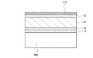
図1は、本発明の一態様における光電変換装置の断面図であり、基板100上に第1の電極110、透光性半導体層130、第1のシリコン半導体層140、第2のシリコン半導体層150、第2の電極120が順に積層されている。なお、図1の構成の光電変換装置は、基板100側が受光面となるが、基板100上に形成する積層の順序を上記とは逆にして、基板100とは逆側を受光面としても良い。
FIG. 1 is a cross-sectional view of a photoelectric conversion device according to one embodiment of the present invention, in which a
基板100には、例えば、青板ガラス、白板ガラス、鉛ガラス、または結晶化ガラスなどのガラス基板を用いることができる。また、アルミノシリケートガラス、バリウムホウケイ酸ガラス、またはアルミノホウケイ酸ガラスなどの無アルカリガラス基板や石英基板を用いることができる。本実施の形態では、基板100にガラス基板を用いる。
As the
また、基板100には、樹脂基板を用いることもできる。例えば、ポリエーテルスルホン(PES)、ポリエチレンテレフタレート(PET)、ポリエチレンナフタレート(PEN)、ポリカーボネート(PC)、ポリアミド系合成繊維、ポリエーテルエーテルケトン(PEEK)、ポリスルホン(PSF)、ポリエーテルイミド(PEI)、ポリアリレート(PAR)、ポリブチレンテレフタレート(PBT)、ポリイミド、アクリロニトリルブタジエンスチレン樹脂、ポリ塩化ビニル、ポリプロピレン、ポリ酢酸ビニル、アクリル樹脂などが挙げられる。
The
第1の電極110には、例えば、インジウム錫酸化物、珪素を含むインジウム錫酸化物(、亜鉛を含む酸化インジウム、酸化亜鉛、ガリウムを含む酸化亜鉛、アルミニウムを含む酸化亜鉛、酸化錫、フッ素を含む酸化錫、またはアンチモンを含む酸化錫等の透光性導電膜を用いることができる。上記透光性導電膜は単層に限らず、異なる膜の積層でも良い。例えば、インジウム錫酸化物とアルミニウムを含む酸化亜鉛の積層や、インジウム錫酸化物とフッ素を含む酸化錫の積層などを用いることができる。膜厚は総厚で10nm以上1000nm以下とする。
For the
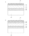
また、図2(A)に示すように、第1の電極110の表面に凹凸を設けた構成としても良い。第1の電極110の表面に凹凸を設けることで、その上に積層する各層の界面にも凹凸が形成することができる。該凹凸により、基板表面での多重反射、光電変換層内での光路長の増大、及び裏面反射光の表面での全反射効果(光閉じ込め効果)が付与され、光電変換装置の電気特性を向上させることができる。
Further, as illustrated in FIG. 2A, a structure in which unevenness is provided on the surface of the
また、第2の電極120には、アルミニウム、チタン、ニッケル、銀、モリブデン、タンタル、タングステン、クロム、銅またはステンレス等の金属膜を用いることができる。金属膜は単層に限らず、異なる膜の積層でも良い。例えば、ステンレスとアルミニウムの積層や、銀とアルミニウムの積層などを用いることができる。膜厚は総厚で100nm以上600nm以下、好ましくは100nm以上300nm以下とする。
The
なお、図2(B)に示すように、第2の電極120と第2のシリコン半導体層150との間に、上述した材料の透光性導電膜190を形成した構成であっても良い。該透光性導電膜190を設けることで光が反射する界面を増やすことができ、光電変換装置の電気特性を向上させることができる。このとき、該透光性導電膜190の膜厚は、10nm以上100nm以下とすることが好ましい。例えば、半導体層側からインジウム錫酸化物、銀、アルミニウムの順で形成した積層を用いることができる。なお、図2(B)では、第1の電極110に凹凸を形成した構成を例示しているが、該凹凸の無い構成であっても良い。
Note that as illustrated in FIG. 2B, a light-transmitting
透光性半導体層130は、無機化合物と有機化合物の複合材料である。該無機化合物としては、遷移金属酸化物を用いることができ、特に元素周期表における第4族乃至第8族に属する金属の酸化物であることが好ましい。具体的には酸化バナジウム、酸化ニオブ、酸化タンタル、酸化クロム、酸化モリブデン、酸化タングステン、酸化マンガン、酸化レニウムなどを用いることができる。中でも特に、酸化モリブデンは大気中でも安定であり、吸湿性が低く、扱いやすいため好ましい。
The light-transmitting
また、上記有機化合物としては、芳香族アミン化合物、カルバゾール誘導体、芳香族炭化水素、高分子化合物(オリゴマー、デンドリマー、ポリマー等)、ジベンゾフラン骨格もしくはジベンゾチオフェン骨格を含む複素環化合物など、種々の化合物を用いることができる。なお、複合材料に用いる有機化合物としては、正孔輸送性の高い有機化合物を用いる。具体的には、10−6cm2/Vs以上の正孔移動度を有する物質であることが好ましい。但し、電子よりも正孔の輸送性の高い物質であれば、これら以外のものを用いてもよい。 Examples of the organic compound include various compounds such as aromatic amine compounds, carbazole derivatives, aromatic hydrocarbons, polymer compounds (oligomers, dendrimers, polymers, etc.), heterocyclic compounds containing a dibenzofuran skeleton or a dibenzothiophene skeleton. Can be used. Note that as the organic compound used for the composite material, an organic compound having a high hole-transport property is used. Specifically, a substance having a hole mobility of 10 −6 cm 2 / Vs or higher is preferable. Note that other than these substances, any substance that has a property of transporting more holes than electrons may be used.
上述の遷移金属酸化物は電子受容性を有し、正孔輸送性の高い有機化合物との複合材料はキャリア密度が高く、p型の半導体特性を示す。また、該複合材料は、可視光域から赤外域の広い波長範囲に渡って透過率が高い特性を有している。 The above-described transition metal oxide has an electron accepting property, and a composite material with an organic compound having a high hole transporting property has a high carrier density and exhibits p-type semiconductor characteristics. In addition, the composite material has a characteristic of high transmittance over a wide wavelength range from the visible light region to the infrared region.
また、該複合材料は安定であり、シリコン層との界面に酸化シリコンを生じさせないことから界面の欠陥を低減させることができ、キャリアのライフタイムを向上させることができる。 In addition, since the composite material is stable and does not generate silicon oxide at the interface with the silicon layer, defects at the interface can be reduced, and the lifetime of carriers can be improved.
該複合材料をn型の単結晶シリコン基板の両面に成膜し、パッシベーション膜としたときのキャリアのライフタイムは、有機化合物に4−フェニル−4’−(9−フェニルフルオレン−9−イル)トリフェニルアミン(略称:BPAFLP)、無機化合物に酸化モリブデン(VI)を用いた場合で、700μsec以上、有機化合物に4,4’−ビス[N−(1−ナフチル)−N−フェニルアミノ]ビフェニル(略称:NPB)、無機化合物に酸化モリブデン(VI)を用いた場合で、400μsec以上であることが実験で確かめられている。なお、パッシベーション膜を形成しないn型の単結晶シリコン基板のライフタイムは、約40μsec、該単結晶シリコン基板の両面にスパッタ法でインジウム錫酸化物(ITO)を成膜した場合のライフタイムは、約30μsecである。 When the composite material is formed on both surfaces of an n-type single crystal silicon substrate to form a passivation film, the lifetime of the carrier is 4-phenyl-4 ′-(9-phenylfluoren-9-yl) as an organic compound. When triphenylamine (abbreviation: BPAFLP) and molybdenum (VI) oxide are used as the inorganic compound, 700 μsec or more, and 4,4′-bis [N- (1-naphthyl) -N-phenylamino] biphenyl as the organic compound (Abbreviation: NPB), when molybdenum oxide (VI) is used as the inorganic compound, it has been confirmed by experiments that it is 400 μsec or more. Note that the lifetime of an n-type single crystal silicon substrate that does not form a passivation film is about 40 μsec, and the lifetime when indium tin oxide (ITO) is formed on both surfaces of the single crystal silicon substrate by sputtering is as follows: About 30 μsec.
第1のシリコン半導体層140には、i型のシリコン半導体を用いる。なお、本明細書において、i型の半導体とは、フェルミ準位がバンドギャップの中央に位置する所謂真性半導体の他、半導体に含まれるp型を付与する不純物及びn型を付与する不純物が共に1×1020cm−3以下の濃度であり、暗伝導度に対して光伝導度が100倍以上である半導体を指す。このi型のシリコン半導体には、周期表第13族または第15族の元素が不純物として含まれるものであっても良い。
An i-type silicon semiconductor is used for the first
第1のシリコン半導体層140に用いるi型のシリコン半導体には、非単結晶シリコン、非晶質シリコン、微結晶シリコン、または多結晶シリコンを用いることが好ましい。非晶質シリコンは、可視光領域に分光感度のピークを有しており、蛍光灯下のような低照度の環境で高い光電変換能力を示す光電変換装置を形成することができる。また、微結晶シリコン及び多結晶シリコンは、可視光領域よりも長波長側の波長領域に分光感度のピークを有しており、太陽光を光源とする屋外で高い光電変換能力を示す光電変換装置を形成することができる。なお、第1のシリコン半導体層140に非晶質シリコンを用いる場合の膜厚は、100nm以上600nm以下とすることが好ましく、微結晶シリコンまたは多結晶シリコンを用いる場合の膜厚は、1μm以上100μm以下とすることが好ましい。
As the i-type silicon semiconductor used for the first
第2のシリコン半導体層150にはn型のシリコン半導体膜を用いる。なお、第2のシリコン半導体層150の膜厚は、3nm以上50nm以下とすることが好ましい。また、第2のシリコン半導体層150には非晶質シリコンを用いることもできるが、より低抵抗の微結晶シリコンまたは多結晶シリコンを用いることが好ましい。
An n-type silicon semiconductor film is used for the second
以上説明した、p型の透光性半導体層130、i型の第1のシリコン半導体層140、n型の第2のシリコン半導体層150の積層によりp−i−n型の接合を形成することができる。
A p-i-n type junction is formed by stacking the p-type
また、図3に示すように、基板200上に、第1の電極210、第1の透光性半導体層230、第1のシリコン半導体層240、第2のシリコン半導体層250、第2の透光性半導体層260、第3のシリコン半導体層270、第4のシリコン半導体層280、第2の電極220を設けた構成としても良い。該構成の光電変換装置は、第1のシリコン半導体層240を光吸収層とするトップセルと、第3のシリコン半導体層270を光吸収層とするボトムセルを直列に接続した、所謂タンデム型の光電変換装置である。
Further, as illustrated in FIG. 3, the
図3の光電変換装置では、第1のシリコン半導体層240に非晶質シリコンを用い、第3のシリコン半導体層270に微結晶シリコンまたは多結晶シリコンを用いる。また、第1の透光性半導体層230及び第2の透光性半導体層260には、前述した透光性半導体層130と同様の材料を用いることができ、第2のシリコン半導体層250及び第4のシリコン半導体層280には、前述した第2のシリコン半導体層150と同様の材料を用いることができる。
In the photoelectric conversion device in FIG. 3, amorphous silicon is used for the first
基板200側から第1の電極210を透過してトップセルに侵入した光のうち、主に可視光から短波長側の光は、第1のシリコン半導体層240において光電変換され、トップセルを透過する主に可視光よりも長波長側の光は、第3のシリコン半導体層270で光電変換される。従って、広い波長範囲の光を有効に利用することができ、光電変換装置の変換効率を向上させることができる。
Of the light that has passed through the
従来の光電変換装置では、不純物の添加により低抵抗化させた非晶質シリコンまたは微結晶シリコン等を窓層としていたため、窓層は光吸収層とほぼ同じ光吸収特性を有していた。この窓層においても光キャリアは発生するが、少数キャリアの寿命が短く、電流として取り出すことができないため、窓層における光吸収は大きな損失となっていた。 In the conventional photoelectric conversion device, since the window layer is made of amorphous silicon, microcrystalline silicon, or the like whose resistance is reduced by adding impurities, the window layer has almost the same light absorption characteristics as the light absorption layer. Even in this window layer, optical carriers are generated, but the minority carrier has a short lifetime and cannot be taken out as a current. Therefore, light absorption in the window layer is a large loss.
本発明の一態様では、無機化合物と有機化合物の複合材料からなるp型の透光性半導体層を窓層として用いることにより、窓層での光吸収損失が低減し、i型の光吸収層において効率良く光電変換を行うことできるようになる。また、前述したように、該複合材料は、シリコン表面のパッシベーション効果が非常に高い。従って、光電変換装置の変換効率を向上させることができる。 In one embodiment of the present invention, by using a p-type light-transmitting semiconductor layer made of a composite material of an inorganic compound and an organic compound as a window layer, light absorption loss in the window layer is reduced, and an i-type light absorption layer In this case, photoelectric conversion can be performed efficiently. Further, as described above, the composite material has a very high silicon surface passivation effect. Therefore, the conversion efficiency of the photoelectric conversion device can be improved.
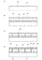
次に、本発明の一態様における光電変換装置の作製方法について図4を用いて説明する。以下に示す光電変換装置の作製方法は、図1の光電変換装置を直列に複数接続した集積型光電変換装置の作製方法であり、完成した構造は、図4(D)に示されている。 Next, a method for manufacturing a photoelectric conversion device according to one embodiment of the present invention is described with reference to FIGS. The photoelectric conversion device manufacturing method described below is a manufacturing method of an integrated photoelectric conversion device in which a plurality of photoelectric conversion devices in FIG. 1 are connected in series, and a completed structure is illustrated in FIG.
まず、基板100上に第1の電極110となる透光性導電膜を形成する。ここでは、スパッタ法を用い、膜厚100nmのインジウム錫酸化物(ITO)を形成する。なお、図2に示すような透光性導電膜の凹凸は、例えば酸化亜鉛系の透光性導電膜を塩酸などの強酸でエッチングすることで容易に形成することができる。
First, a light-transmitting conductive film to be the
本実施の形態では基板100にガラス基板を用いるが、例えば100μm前後の樹脂基板を用いれば、Roll−to−Rollプロセスを行うことができる。
In this embodiment, a glass substrate is used as the
Roll−to−Rollプロセスには、スパッタ法やプラズマCVD法などの成膜工程だけでなく、スクリーン印刷法やレーザ加工法などの工程も含まれる。従って、光電変換装置のほぼ全ての製造工程をRoll−to−Rollプロセスで行うこともできる。また、途中までの工程をRoll−to−Rollプロセスで行い、シート状に分断して、その後の工程をシート単位で行っても良い。例えば、分断したシートをセラミックや金属、またはそれらの複合体等で形成された枠に貼付けることで、ガラス基板等と同様に取り扱うことができる。 The Roll-to-Roll process includes not only film forming processes such as sputtering and plasma CVD, but also processes such as screen printing and laser processing. Therefore, almost all manufacturing steps of the photoelectric conversion device can be performed by a Roll-to-Roll process. Further, the process up to the middle may be performed by a Roll-to-Roll process, divided into sheets, and the subsequent processes may be performed on a sheet basis. For example, the cut sheet can be handled in the same manner as a glass substrate or the like by sticking it to a frame formed of ceramic, metal, or a composite thereof.
次に、該透光性導電膜を複数に分離する第1の分離溝310を形成する(図4(A)参照)。該分離溝は、レーザ加工等で形成することができる。このレーザ加工に用いられるレーザは、可視光領域または赤外光領域の連続発振またはパルス発振レーザを用いることが好ましい。例えば、Nd−YAGレーザの基本波(波長1064nm)や第二高調波(波長532nm)を用いることができる。なお、ここで該分離溝の一部が基板100に達しても良い。また、この段階で透光性導電膜が分離加工されることにより第1の電極110が形成される。
Next, a
次に、第1の電極110及び第1の分離溝310上に、透光性半導体層130を形成する。透光性半導体層130は、前述した無機化合物及び有機化合物の共蒸着法により形成する。共蒸着法とは、一つの成膜室内で複数の蒸発源から同時に蒸着を行う蒸着法である。成膜は高真空下で行われることが好ましい。高真空は、成膜室内を真空排気手段により真空度が5×10⁻³Pa以下、好ましくは10−4Pa乃至10−6Pa程度の範囲なるように真空排気することで得られる。
Next, the light-transmitting
本実施の形態では、透光性半導体層130は、4−フェニル−4’−(9−フェニルフルオレン−9−イル)トリフェニルアミン(略称:BPAFLP)及び酸化モリブデン(VI)を共蒸着することにより形成する。その膜厚は、50nmとし、BPAFLPと酸化モリブデンの比率は、重量比で2:1(=BPAFLP:酸化モリブデン)となるように調節する。
In this embodiment, the light-transmitting
次に、プラズマCVD法を用いて、第1のシリコン半導体層140として膜厚600nmのi型の非晶質シリコンを成膜する。原料ガスには、シランまたはジシランを用いることができ、水素を添加しても良い。このとき、膜中に含まれる大気成分がドナーとなる場合があるため、導電型がよりi型に近づくように、原料ガス中にホウ素(B)を添加しても良い。この場合、i型の非晶質シリコン中のホウ素濃度が0.001at.%以上0.1at.%以下となる様にする。
Next, i-type amorphous silicon with a thickness of 600 nm is formed as the first
次に、第2のシリコン半導体層150として、膜厚30nmのn型の微結晶シリコンを成膜する(図4(B)参照)。本実施の形態では、プラズマCVD法を用い、n型を付与する不純物を含むドーピングガスを原料ガスに混合してn型の微結晶シリコンを形成する。n型を付与する不純物としては、代表的には周期表第15族元素であるリン、ヒ素、またはアンチモンなどが挙げられる。例えば、ホスフィンなどのドーピングガスをシラン等の原料ガスに混合することで、n型の微結晶シリコンを形成することができる。なお、第2のシリコン半導体層150は、非晶質シリコンで形成しても良いが、より低抵抗な微結晶シリコンで形成することが好ましい。
Next, n-type microcrystalline silicon with a thickness of 30 nm is formed as the second silicon semiconductor layer 150 (see FIG. 4B). In this embodiment mode, a plasma CVD method is used, and a doping gas containing an impurity imparting n-type is mixed with a source gas to form n-type microcrystalline silicon. Typical examples of the impurity imparting n-type include phosphorus, arsenic, antimony, and the like, which are Group 15 elements of the periodic table. For example, n-type microcrystalline silicon can be formed by mixing a doping gas such as phosphine with a source gas such as silane. Note that the second
次に、透光性半導体層130、第1のシリコン半導体層140及び第2のシリコン半導体層150の積層を複数に分離する第2の分離溝320を形成する(図4(C)参照)。該分離溝は、レーザ加工等で形成することができる。このレーザ加工に用いられるレーザは、可視光領域の連続発振またはパルス発振レーザを用いることが好ましい。例えば、Nd−YAGレーザの第二高調波(波長532nm)などを用いることができる。なお、図2(B)に示すような透光性導電膜を設ける場合は、第2の分離溝320を形成する前に第2のシリコン半導体層150上に透光性導電膜を形成しておけば良い。
Next, a
次に、第2の分離溝320を充填し、かつ第2のシリコン半導体層150を覆う様に導電膜を形成する。ここでは、スパッタ法を用い、膜厚5nmの銀と膜厚300nmのアルミニウムを順に積層する。
Next, a conductive film is formed so as to fill the
そして、該導電膜を複数に分離する第3の分離溝330を形成する(図4(D)参照)。該分離溝は、レーザ加工等で形成することができる。このレーザ加工に用いられるレーザは、赤外光領域の連続発振またはパルス発振レーザを用いることが好ましい。例えば、Nd−YAGレーザの基本波(波長1064nm)などを用いることができる。また、この段階で導電膜が分離加工されることにより第2の電極120、第1の端子410及び第2の端子420が形成される。ここで、第1の端子410及び第2の端子420は取り出し電極となる。
Then, a
以上により、本発明の一態様の光電変換装置を作製することができる。なお、本実施の形態では、図1に例示した光電変換装置を集積化した構成の作製方法を説明したが、図2(A)、図2(B)、及び図3の構成の光電変換装置を同様の方法で集積化することもできる。 Through the above steps, the photoelectric conversion device of one embodiment of the present invention can be manufactured. Note that although a method for manufacturing a structure in which the photoelectric conversion devices illustrated in FIG. 1 are integrated is described in this embodiment mode, the photoelectric conversion devices having the structures in FIG. 2A, FIG. 2B, and FIG. Can be integrated in a similar manner.
本実施の形態は、他の実施の形態に記載した構成と適宜組み合わせて実施することが可能である。 This embodiment can be implemented in appropriate combination with the structures described in the other embodiments.
(実施の形態2)
本実施の形態では、実施の形態1で示した透光性半導体層について説明する。
(Embodiment 2)
In this embodiment, the light-transmitting semiconductor layer described in Embodiment 1 will be described.
実施の形態1で示した光電変換装置における透光性半導体層130、230、260には、遷移金属酸化物と有機化合物とを複合した材料を用いることができる。なお、本明細書中において、複合とは、単に2つの材料を混合させるだけでなく、複数の材料を混合することによって材料間での電荷の授受が行われ得る状態になることを言う。
For the light-transmitting
上記遷移金属酸化物としては、電子受容性を有する遷移金属酸化物を用いることができる。具体的には、遷移金属酸化物の中でも、元素周期表における第4族乃至第8族に属する金属の酸化物であることが好ましい。特に、酸化バナジウム、酸化ニオブ、酸化タンタル、酸化クロム、酸化モリブデン、酸化タングステン、酸化マンガン、酸化レニウムは電子受容性が高いため好ましい。中でも特に、酸化モリブデンは大気中でも安定であり、吸湿性が低く、扱いやすいため好ましい。 As the transition metal oxide, a transition metal oxide having an electron accepting property can be used. Specifically, among transition metal oxides, an oxide of a metal belonging to Groups 4 to 8 in the periodic table is preferable. In particular, vanadium oxide, niobium oxide, tantalum oxide, chromium oxide, molybdenum oxide, tungsten oxide, manganese oxide, and rhenium oxide are preferable because of their high electron-accepting properties. Among these, molybdenum oxide is especially preferable because it is stable in the air, has a low hygroscopic property, and is easy to handle.
また、上記有機化合物としては、芳香族アミン化合物、カルバゾール誘導体、芳香族炭化水素、高分子化合物(オリゴマー、デンドリマー、ポリマー等)、ジベンゾフラン骨格もしくはジベンゾチオフェン骨格を含む複素環化合物など、種々の化合物を用いることができる。なお、複合材料に用いる有機化合物としては、正孔輸送性の高い有機化合物を用いる。具体的には、10−6cm2/Vs以上の正孔移動度を有する物質であることが好ましい。但し、電子よりも正孔の輸送性の高い物質であれば、これら以外のものを用いてもよい。 Examples of the organic compound include various compounds such as aromatic amine compounds, carbazole derivatives, aromatic hydrocarbons, polymer compounds (oligomers, dendrimers, polymers, etc.), heterocyclic compounds containing a dibenzofuran skeleton or a dibenzothiophene skeleton. Can be used. Note that as the organic compound used for the composite material, an organic compound having a high hole-transport property is used. Specifically, a substance having a hole mobility of 10 −6 cm 2 / Vs or higher is preferable. Note that other than these substances, any substance that has a property of transporting more holes than electrons may be used.
上記遷移金属酸化物と上記有機化合物とを含む複合材料では、有機化合物の最高被占有軌道準位(HOMO準位)にある電子が、遷移金属酸化物の伝導帯に移動することにより、遷移金属酸化物と有機化合物との間に相互作用が生じる。この相互作用により、遷移金属酸化物と有機化合物とを含む複合材料は、キャリア密度が高く、p型の半導体特性を示す。 In the composite material including the transition metal oxide and the organic compound, electrons in the highest occupied orbital level (HOMO level) of the organic compound move to the conduction band of the transition metal oxide, whereby the transition metal Interaction occurs between the oxide and the organic compound. Due to this interaction, a composite material including a transition metal oxide and an organic compound has a high carrier density and exhibits p-type semiconductor characteristics.
以下では、複合材料に用いることのできる有機化合物を具体的に列挙する。 Below, the organic compound which can be used for a composite material is listed concretely.
例えば、複合材料に用いることのできる芳香族アミン化合物としては、例えば、4,4’−ビス[N−(1−ナフチル)−N−フェニルアミノ]ビフェニル(略称:NPB)、N,N’−ビス(3−メチルフェニル)−N,N’−ジフェニル−[1,1’−ビフェニル]−4,4’−ジアミン(略称:TPD)、4,4’,4’’−トリス(N,N−ジフェニルアミノ)トリフェニルアミン(略称:TDATA)、4,4’,4’’−トリス[N−(3−メチルフェニル)−N−フェニルアミノ]トリフェニルアミン(略称:MTDATA)、N,N’−ビス(スピロ−9,9’−ビフルオレン−2−イル)−N,N’−ジフェニルベンジジン(略称:BSPB)等を用いることができる。また、N,N’−ビス(4−メチルフェニル)−N,N’−ジフェニル−p−フェニレンジアミン(略称:DTDPPA)、4,4’−ビス[N−(4−ジフェニルアミノフェニル)−N−フェニルアミノ]ビフェニル(略称:DPAB)、N,N’−ビス[4−[ビス(3−メチルフェニル)アミノ]フェニル]−N,N’−ジフェニル−[1,1’−ビフェニル]−4,4’−ジアミン(略称:DNTPD)、1,3,5−トリス[N−(4−ジフェニルアミノフェニル)−N−フェニルアミノ]ベンゼン(略称:DPA3B)、4−フェニル−4’−(9−フェニルフルオレン−9−イル)トリフェニルアミン(略称:BPAFLP)、4,4’−ビス[N−(9,9−ジメチルフルオレン−2−イル)−N−フェニルアミノ]ビフェニル(略称:DFLDPBi)等を挙げることができる。 For example, as an aromatic amine compound that can be used for the composite material, for example, 4,4′-bis [N- (1-naphthyl) -N-phenylamino] biphenyl (abbreviation: NPB), N, N′— Bis (3-methylphenyl) -N, N′-diphenyl- [1,1′-biphenyl] -4,4′-diamine (abbreviation: TPD), 4,4 ′, 4 ″ -tris (N, N -Diphenylamino) triphenylamine (abbreviation: TDATA), 4,4 ', 4 "-tris [N- (3-methylphenyl) -N-phenylamino] triphenylamine (abbreviation: MTDATA), N, N '-Bis (spiro-9,9'-bifluoren-2-yl) -N, N'-diphenylbenzidine (abbreviation: BSPB) or the like can be used. N, N′-bis (4-methylphenyl) -N, N′-diphenyl-p-phenylenediamine (abbreviation: DTDPPA), 4,4′-bis [N- (4-diphenylaminophenyl) -N -Phenylamino] biphenyl (abbreviation: DPAB), N, N'-bis [4- [bis (3-methylphenyl) amino] phenyl] -N, N'-diphenyl- [1,1'-biphenyl] -4 , 4′-diamine (abbreviation: DNTPD), 1,3,5-tris [N- (4-diphenylaminophenyl) -N-phenylamino] benzene (abbreviation: DPA3B), 4-phenyl-4 ′-(9 -Phenylfluoren-9-yl) triphenylamine (abbreviation: BPAFLP), 4,4'-bis [N- (9,9-dimethylfluoren-2-yl) -N-phenylamino] biphe Le (abbreviation: DFLDPBi), and the like can be given.
複合材料に用いることのできるカルバゾール誘導体としては、具体的には、3−[N−(9−フェニルカルバゾール−3−イル)−N−フェニルアミノ]−9−フェニルカルバゾール(略称:PCzPCA1)、3,6−ビス[N−(9−フェニルカルバゾール−3−イル)−N−フェニルアミノ]−9−フェニルカルバゾール(略称:PCzPCA2)、3−[N−(1−ナフチル)−N−(9−フェニルカルバゾール−3−イル)アミノ]−9−フェニルカルバゾール(略称:PCzPCN1)等を挙げることができる。 Specific examples of the carbazole derivative that can be used for the composite material include 3- [N- (9-phenylcarbazol-3-yl) -N-phenylamino] -9-phenylcarbazole (abbreviation: PCzPCA1), 3 , 6-Bis [N- (9-phenylcarbazol-3-yl) -N-phenylamino] -9-phenylcarbazole (abbreviation: PCzPCA2), 3- [N- (1-naphthyl) -N- (9- Phenylcarbazol-3-yl) amino] -9-phenylcarbazole (abbreviation: PCzPCN1) and the like.
複合材料に用いることのできるカルバゾール誘導体としては、4,4’−ジ(N−カルバゾリル)ビフェニル(略称:CBP)、1,3,5−トリス[4−(N−カルバゾリル)フェニル]ベンゼン(略称:TCPB)、9−[4−(N−カルバゾリル)フェニル]−10−フェニルアントラセン(略称:CzPA)、1,4−ビス[4−(N−カルバゾリル)フェニル]−2,3,5,6−テトラフェニルベンゼン等を用いることができる。 As the carbazole derivative which can be used for the composite material, 4,4′-di (N-carbazolyl) biphenyl (abbreviation: CBP), 1,3,5-tris [4- (N-carbazolyl) phenyl] benzene (abbreviation) : TCPB), 9- [4- (N-carbazolyl) phenyl] -10-phenylanthracene (abbreviation: CzPA), 1,4-bis [4- (N-carbazolyl) phenyl] -2,3,5,6 -Tetraphenylbenzene or the like can be used.
複合材料に用いることのできる芳香族炭化水素としては、例えば、2−tert−ブチル−9,10−ジ(2−ナフチル)アントラセン(略称:t−BuDNA)、2−tert−ブチル−9,10−ジ(1−ナフチル)アントラセン、9,10−ビス(3,5−ジフェニルフェニル)アントラセン(略称:DPPA)、2−tert−ブチル−9,10−ビス(4−フェニルフェニル)アントラセン(略称:t−BuDBA)、9,10−ジ(2−ナフチル)アントラセン(略称:DNA)、9,10−ジフェニルアントラセン(略称:DPAnth)、2−tert−ブチルアントラセン(略称:t−BuAnth)、9,10−ビス(4−メチル−1−ナフチル)アントラセン(略称:DMNA)、9,10−ビス[2−(1−ナフチル)フェニル]−2−tert−ブチルアントラセン、9,10−ビス[2−(1−ナフチル)フェニル]アントラセン、2,3,6,7−テトラメチル−9,10−ジ(1−ナフチル)アントラセン、2,3,6,7−テトラメチル−9,10−ジ(2−ナフチル)アントラセン、9,9’−ビアントリル、10,10’−ジフェニル−9,9’−ビアントリル、10,10’−ビス(2−フェニルフェニル)−9,9’−ビアントリル、10,10’−ビス[(2,3,4,5,6−ペンタフェニル)フェニル]−9,9’−ビアントリル、アントラセン、テトラセン、ルブレン、ペリレン、2,5,8,11−テトラ(tert−ブチル)ペリレン等が挙げられる。また、この他、ペンタセン、コロネン等も用いることができる。このように、1×10−6cm2/Vs以上の正孔移動度を有し、炭素数14〜42である芳香族炭化水素を用いることがより好ましい。 Examples of aromatic hydrocarbons that can be used for the composite material include 2-tert-butyl-9,10-di (2-naphthyl) anthracene (abbreviation: t-BuDNA), 2-tert-butyl-9,10. -Di (1-naphthyl) anthracene, 9,10-bis (3,5-diphenylphenyl) anthracene (abbreviation: DPPA), 2-tert-butyl-9,10-bis (4-phenylphenyl) anthracene (abbreviation: t-BuDBA), 9,10-di (2-naphthyl) anthracene (abbreviation: DNA), 9,10-diphenylanthracene (abbreviation: DPAnth), 2-tert-butylanthracene (abbreviation: t-BuAnth), 9, 10-bis (4-methyl-1-naphthyl) anthracene (abbreviation: DMNA), 9,10-bis [2- (1-naphthy ) Phenyl] -2-tert-butylanthracene, 9,10-bis [2- (1-naphthyl) phenyl] anthracene, 2,3,6,7-tetramethyl-9,10-di (1-naphthyl) anthracene 2,3,6,7-tetramethyl-9,10-di (2-naphthyl) anthracene, 9,9′-bianthryl, 10,10′-diphenyl-9,9′-bianthryl, 10,10′- Bis (2-phenylphenyl) -9,9′-bianthryl, 10,10′-bis [(2,3,4,5,6-pentaphenyl) phenyl] -9,9′-bianthryl, anthracene, tetracene, Examples include rubrene, perylene, 2,5,8,11-tetra (tert-butyl) perylene, and the like. In addition, pentacene, coronene, and the like can also be used. Thus, it is more preferable to use an aromatic hydrocarbon having a hole mobility of 1 × 10 −6 cm 2 / Vs or more and having 14 to 42 carbon atoms.
複合材料に用いることのできる芳香族炭化水素は、ビニル骨格を有していてもよい。ビニル基を有している芳香族炭化水素としては、例えば、4,4’−ビス(2,2−ジフェニルビニル)ビフェニル(略称:DPVBi)、9,10−ビス[4−(2,2−ジフェニルビニル)フェニル]アントラセン(略称:DPVPA)等が挙げられる。 The aromatic hydrocarbon that can be used for the composite material may have a vinyl skeleton. As the aromatic hydrocarbon having a vinyl group, for example, 4,4′-bis (2,2-diphenylvinyl) biphenyl (abbreviation: DPVBi), 9,10-bis [4- (2,2- Diphenylvinyl) phenyl] anthracene (abbreviation: DPVPA) and the like.
また、複合材料に用いることのできる有機化合物は、ジベンゾフラン骨格もしくはジベンゾチオフェン骨格を含む複素環化合物であっても良い。 The organic compound that can be used for the composite material may be a heterocyclic compound including a dibenzofuran skeleton or a dibenzothiophene skeleton.
また、複合材料に用いることのできる有機化合物は、高分子化合物であってもよく、例えば、ポリ(N−ビニルカルバゾール)(略称:PVK)、ポリ(4−ビニルトリフェニルアミン)(略称:PVTPA)、ポリ[N−(4−{N’−[4−(4−ジフェニルアミノ)フェニル]フェニル−N’−フェニルアミノ}フェニル)メタクリルアミド](略称:PTPDMA)ポリ[N,N’−ビス(4−ブチルフェニル)−N,N’−ビス(フェニル)ベンジジン](略称:Poly−TPD)などを用いても良い。 The organic compound that can be used for the composite material may be a high molecular compound, such as poly (N-vinylcarbazole) (abbreviation: PVK), poly (4-vinyltriphenylamine) (abbreviation: PVTPA). ), Poly [N- (4- {N ′-[4- (4-diphenylamino) phenyl] phenyl-N′-phenylamino} phenyl) methacrylamide] (abbreviation: PTPDMA) poly [N, N′-bis (4-Butylphenyl) -N, N′-bis (phenyl) benzidine] (abbreviation: Poly-TPD) or the like may be used.
本実施の形態で示す透光性半導体層は、非晶質シリコン、微結晶シリコンまたは多結晶シリコンが光吸収を示す波長範囲において透光性に優れているため、シリコン半導体層を窓層に用いるよりも厚く形成することができ、抵抗損失を低減させることができる。 The light-transmitting semiconductor layer described in this embodiment has excellent light-transmitting properties in a wavelength range where amorphous silicon, microcrystalline silicon, or polycrystalline silicon absorbs light, and thus the silicon semiconductor layer is used for a window layer. Therefore, it is possible to reduce the resistance loss.
図5は、4−フェニル−4’−(9−フェニルフルオレン−9−イル)トリフェニルアミン(略称:BPAFLP)及び酸化モリブデン(VI)を共蒸着することにより得られる透光性半導体層(膜厚57nm)及び非晶質シリコン層(膜厚10nm)の分光透過率、並びに一般的な非晶質シリコン光電変換装置の分光感度特性を示したものである。図5に示すように、本実施の形態における透光性半導体層は広い波長範囲で高い透光性を有しているのに対し、非晶質シリコン層は可視光より短波長側での吸収が大きいことがわかる。例えば、非晶質シリコン膜を窓層に用いた従来の光電変換装置を想定すると、この可視光より短波長側の吸収が損失となる。一方で、透光性半導体層を窓層に用いれば非晶質シリコン膜の吸収がある波長範囲の光も有効に光電変換に用いることができる。 FIG. 5 shows a light-transmitting semiconductor layer (film) obtained by co-evaporation of 4-phenyl-4 ′-(9-phenylfluoren-9-yl) triphenylamine (abbreviation: BPAFLP) and molybdenum oxide (VI). The spectral transmittance of a 57 nm thick) and amorphous silicon layer (10 nm thick) and the spectral sensitivity characteristics of a typical amorphous silicon photoelectric conversion device are shown. As shown in FIG. 5, the translucent semiconductor layer in this embodiment has high translucency in a wide wavelength range, whereas the amorphous silicon layer absorbs light on a shorter wavelength side than visible light. Can be seen to be large. For example, assuming a conventional photoelectric conversion device using an amorphous silicon film as a window layer, the absorption on the shorter wavelength side than visible light becomes a loss. On the other hand, if a light-transmitting semiconductor layer is used for the window layer, light in a wavelength range in which the amorphous silicon film is absorbed can be effectively used for photoelectric conversion.
上述の透光性半導体層の形成方法としては、乾式法、湿式法を問わず、種々の方法を用いることができる。乾式法としては、例えば、複数の蒸着源から複数の蒸着材料を気化させて成膜する共蒸着法などが挙げられる。また、湿式法としては、ゾル−ゲル法などを用いて複合材料を含む組成物を調整し、インクジェット法またはスピンコート法などを用いて成膜することができる。 Various methods can be used for forming the light-transmitting semiconductor layer, regardless of a dry method or a wet method. Examples of the dry method include a co-evaporation method in which a plurality of evaporation materials are vaporized from a plurality of evaporation sources to form a film. As a wet method, a composition containing a composite material can be adjusted using a sol-gel method or the like, and a film can be formed using an inkjet method, a spin coating method, or the like.
以上説明した透光性半導体層を光電変換装置の窓層に用いれば、窓層における光吸収損失が低減し、光電変換装置の電気特性を向上させることができる。 When the light-transmitting semiconductor layer described above is used for a window layer of a photoelectric conversion device, light absorption loss in the window layer can be reduced, and electrical characteristics of the photoelectric conversion device can be improved.
本実施の形態は、他の実施の形態に記載した構成と適宜組み合わせて実施することが可能である。 This embodiment can be implemented in appropriate combination with the structures described in the other embodiments.
100 基板
110 第1の電極
120 第2の電極
130 透光性半導体層
140 第1のシリコン半導体層
150 第2のシリコン半導体層
190 透光性導電膜
200 基板
210 第1の電極
220 第2の電極
230 第1の透光性半導体層
240 第1のシリコン半導体層
250 第2のシリコン半導体層
260 第2の透光性半導体層
270 第3のシリコン半導体層
280 第4のシリコン半導体層
310 第1の分離溝
320 第2の分離溝
330 第3の分離溝
410 第1の端子
420 第2の端子
100
Claims (7)
前記第1の電極上に接する領域を有する透光性半導体層と、
前記透光性半導体層上に接する領域を有する第1のシリコン半導体層と、
前記第1のシリコン半導体層上に接する領域を有する第2のシリコン半導体層と、
前記第2のシリコン半導体層上に接する領域を有する第2の電極と、を有し、
前記透光性半導体層は、有機化合物及び無機化合物を有し、
前記透光性半導体層の導電型はp型であり、
前記第1のシリコン半導体層の導電型はi型であり、
前記第2のシリコン半導体層の導電型はn型であり、
前記有機化合物は、ジベンゾフラン骨格もしくはジベンゾチオフェン骨格を含む複素環化合物のいずれかを有することを特徴とする光電変換装置。 A first electrode on the substrate;
A translucent semiconductor layer having a region in contact with the first electrode;
A first silicon semiconductor layer having a region in contact with the translucent semiconductor layer;
A second silicon semiconductor layer having a region in contact with the first silicon semiconductor layer;
A second electrode having a region in contact with the second silicon semiconductor layer,
The translucent semiconductor layer has an organic compound and an inorganic compound,
The conductivity type of the translucent semiconductor layer is p-type,
The conductivity type of the first silicon semiconductor layer is i-type,
The conductivity type of the second silicon semiconductor layer Ri n-type Der,
The organic compound includes any one of a heterocyclic compound including a dibenzofuran skeleton or a dibenzothiophene skeleton .
前記第1のシリコン半導体層は、非単結晶、非晶質、微結晶または多結晶であることを特徴とする光電変換装置。 In claim 1,
The photoelectric conversion device, wherein the first silicon semiconductor layer is non-single crystal, amorphous, microcrystalline, or polycrystalline.
前記第1の電極上に接する領域を有する第1の透光性半導体層と、
前記第1の透光性半導体層上に接する領域を有する第1のシリコン半導体層と、
前記第1のシリコン半導体層上に接する領域を有する第2のシリコン半導体層と、
前記第2のシリコン半導体層上に接する領域を有する第2の透光性半導体層と、
前記第2の透光性半導体層上に接する領域を有する第3のシリコン半導体層と、
前記第3のシリコン半導体層上に接する領域を有する第4のシリコン半導体層と、
前記第4のシリコン半導体層上に接する領域を有する第2の電極と、を有し、
前記第1の透光性半導体層及び前記第2の透光性半導体層の各々は、有機化合物及び無機化合物を有し、
前記第1及び第2の透光性半導体層の導電型はp型であり、
前記第1及び第3のシリコン半導体層の導電型はi型であり、
前記第2及び第4のシリコン半導体層の導電型はn型であり、
前記有機化合物は、ジベンゾフラン骨格もしくはジベンゾチオフェン骨格を含む複素環化合物のいずれかを有することを特徴とする光電変換装置。 A first electrode on the substrate;
A first light-transmissive semiconductor layer having a region in contact with the first electrode;
A first silicon semiconductor layer having a region in contact with the first light-transmissive semiconductor layer;
A second silicon semiconductor layer having a region in contact with the first silicon semiconductor layer;
A second light-transmissive semiconductor layer having a region in contact with the second silicon semiconductor layer;
A third silicon semiconductor layer having a region in contact with the second light-transmitting semiconductor layer;
A fourth silicon semiconductor layer having a region in contact with the third silicon semiconductor layer;
A second electrode having a region in contact with the fourth silicon semiconductor layer,
Each of the first light-transmissive semiconductor layer and the second light-transmissive semiconductor layer has an organic compound and an inorganic compound,
The conductivity type of the first and second translucent semiconductor layers is p-type,
The conductivity types of the first and third silicon semiconductor layers are i-type,
The second and the conductive type fourth silicon semiconductor layer Ri n-type Der,
The organic compound includes any one of a heterocyclic compound including a dibenzofuran skeleton or a dibenzothiophene skeleton .
前記第1のシリコン半導体層は非晶質であり、
前記第3のシリコン半導体層は微結晶または多結晶であることを特徴とする光電変換装置。 In claim 3,
The first silicon semiconductor layer is amorphous;
The photoelectric conversion device, wherein the third silicon semiconductor layer is microcrystalline or polycrystalline.
前記無機化合物は、酸化バナジウム、酸化ニオブ、酸化タンタル、酸化クロム、酸化モリブデン、酸化タングステン、酸化マンガン、酸化レニウムのいずれかを有することを特徴とする光電変換装置。 In any one of Claims 1 thru | or 4,
The photoelectric conversion device, wherein the inorganic compound includes any of vanadium oxide, niobium oxide, tantalum oxide, chromium oxide, molybdenum oxide, tungsten oxide, manganese oxide, and rhenium oxide.
前記有機化合物と前記無機化合物との重量比は2:1であることを特徴とする光電変換装置。 In any one of Claims 1 thru | or 5 ,
The photoelectric conversion device, wherein a weight ratio of the organic compound to the inorganic compound is 2: 1.
前記基板には凹凸はなく、前記第1の電極には凹凸があることを特徴とする光電変換装置。 In any one of Claims 1 thru | or 6 ,
The photoelectric conversion device is characterized in that the substrate has no unevenness and the first electrode has unevenness.
Priority Applications (1)
| Application Number | Priority Date | Filing Date | Title |
|---|---|---|---|
| JP2012034645A JP6000566B2 (en) | 2011-02-21 | 2012-02-21 | Photoelectric conversion device |
Applications Claiming Priority (3)
| Application Number | Priority Date | Filing Date | Title |
|---|---|---|---|
| JP2011034642 | 2011-02-21 | ||
| JP2011034642 | 2011-02-21 | ||
| JP2012034645A JP6000566B2 (en) | 2011-02-21 | 2012-02-21 | Photoelectric conversion device |
Publications (3)
| Publication Number | Publication Date |
|---|---|
| JP2012191188A JP2012191188A (en) | 2012-10-04 |
| JP2012191188A5 JP2012191188A5 (en) | 2015-04-02 |
| JP6000566B2 true JP6000566B2 (en) | 2016-09-28 |
Family
ID=46651740
Family Applications (1)
| Application Number | Title | Priority Date | Filing Date |
|---|---|---|---|
| JP2012034645A Expired - Fee Related JP6000566B2 (en) | 2011-02-21 | 2012-02-21 | Photoelectric conversion device |
Country Status (2)
| Country | Link |
|---|---|
| US (1) | US20120211065A1 (en) |
| JP (1) | JP6000566B2 (en) |
Families Citing this family (4)
| Publication number | Priority date | Publication date | Assignee | Title |
|---|---|---|---|---|
| US9437758B2 (en) | 2011-02-21 | 2016-09-06 | Semiconductor Energy Laboratory Co., Ltd. | Photoelectric conversion device |
| JP2013058562A (en) | 2011-09-07 | 2013-03-28 | Semiconductor Energy Lab Co Ltd | Photoelectric conversion device |
| JP5927027B2 (en) | 2011-10-05 | 2016-05-25 | 株式会社半導体エネルギー研究所 | Photoelectric conversion device |
| JP6108858B2 (en) | 2012-02-17 | 2017-04-05 | 株式会社半導体エネルギー研究所 | P-type semiconductor material and semiconductor device |
Family Cites Families (17)
| Publication number | Priority date | Publication date | Assignee | Title |
|---|---|---|---|---|
| US4292461A (en) * | 1980-06-20 | 1981-09-29 | International Business Machines Corporation | Amorphous-crystalline tandem solar cell |
| US4419533A (en) * | 1982-03-03 | 1983-12-06 | Energy Conversion Devices, Inc. | Photovoltaic device having incident radiation directing means for total internal reflection |
| JPS60240167A (en) * | 1984-05-15 | 1985-11-29 | Semiconductor Energy Lab Co Ltd | Photoelectric conversion device |
| JP2999280B2 (en) * | 1991-02-22 | 2000-01-17 | キヤノン株式会社 | Photovoltaic element |
| US20060021647A1 (en) * | 2004-07-28 | 2006-02-02 | Gui John Y | Molecular photovoltaics, method of manufacture and articles derived therefrom |
| JP5227497B2 (en) * | 2004-12-06 | 2013-07-03 | 株式会社半導体エネルギー研究所 | Method for manufacturing photoelectric conversion element |
| US20070193624A1 (en) * | 2006-02-23 | 2007-08-23 | Guardian Industries Corp. | Indium zinc oxide based front contact for photovoltaic device and method of making same |
| WO2008036769A2 (en) * | 2006-09-19 | 2008-03-27 | Itn Energy Systems, Inc. | Semi-transparent dual layer back contact for bifacial and tandem junction thin-film photovolataic devices |
| US8373060B2 (en) * | 2006-10-24 | 2013-02-12 | Zetta Research and Development LLC—AQT Series | Semiconductor grain microstructures for photovoltaic cells |
| US20080308147A1 (en) * | 2007-06-12 | 2008-12-18 | Yiwei Lu | Rear electrode structure for use in photovoltaic device such as CIGS/CIS photovoltaic device and method of making same |
| US20090139558A1 (en) * | 2007-11-29 | 2009-06-04 | Shunpei Yamazaki | Photoelectric conversion device and manufacturing method thereof |
| EP2075850A3 (en) * | 2007-12-28 | 2011-08-24 | Semiconductor Energy Laboratory Co, Ltd. | Photoelectric conversion device and manufacturing method thereof |
| US7888167B2 (en) * | 2008-04-25 | 2011-02-15 | Semiconductor Energy Laboratory Co., Ltd. | Photoelectric conversion device and method for manufacturing the same |
| US20100269896A1 (en) * | 2008-09-11 | 2010-10-28 | Applied Materials, Inc. | Microcrystalline silicon alloys for thin film and wafer based solar applications |
| CN102165600B (en) * | 2008-09-26 | 2013-09-25 | 株式会社半导体能源研究所 | Photoelectric conversion device and method for manufacturing same |
| US20100089448A1 (en) * | 2008-10-09 | 2010-04-15 | Chun-Chu Yang | Coaxial Solar Cell Structure and Continuous Fabrication Method of its Linear Structure |
| US8563850B2 (en) * | 2009-03-16 | 2013-10-22 | Stion Corporation | Tandem photovoltaic cell and method using three glass substrate configuration |
-
2012
- 2012-02-17 US US13/398,871 patent/US20120211065A1/en not_active Abandoned
- 2012-02-21 JP JP2012034645A patent/JP6000566B2/en not_active Expired - Fee Related
Also Published As
| Publication number | Publication date |
|---|---|
| US20120211065A1 (en) | 2012-08-23 |
| JP2012191188A (en) | 2012-10-04 |
Similar Documents
| Publication | Publication Date | Title |
|---|---|---|
| JP6039154B2 (en) | Photoelectric conversion device | |
| JP5897926B2 (en) | Photoelectric conversion device | |
| US9159939B2 (en) | Photoelectric conversion device | |
| KR101558911B1 (en) | Photoelectric conversion device and manufacturing method thereof | |
| JP5894472B2 (en) | Photoelectric conversion device | |
| JP5577030B2 (en) | Photoelectric conversion device and manufacturing method thereof | |
| CN103594542B (en) | Photovoltaic device and the method for forming photovoltaic device | |
| KR101292061B1 (en) | Thin film solar cell | |
| US8994009B2 (en) | Photoelectric conversion device | |
| JP6000566B2 (en) | Photoelectric conversion device | |
| JP2012191189A (en) | Photoelectric conversion device | |
| KR20110100725A (en) | Solar cell and manufacturing method | |
| US20140048130A1 (en) | Crystalline silicon solar cell water, and solar cell employing the same | |
| KR101529232B1 (en) | Thin-film solar cell and method of fabricating the same | |
| CN103594552B (en) | A kind of manufacture method of photovoltaic cell | |
| US20120132248A1 (en) | Thin film solar cell module | |
| US20130056052A1 (en) | Thin film solar cell | |
| KR20110011048A (en) | Thin-film solar cell, manufacturing method and manufacturing apparatus thereof | |
| WO2013106000A1 (en) | Wire array solar cells employing multiple junctions |
Legal Events
| Date | Code | Title | Description |
|---|---|---|---|
| A521 | Request for written amendment filed |
Free format text: JAPANESE INTERMEDIATE CODE: A523 Effective date: 20150210 |
|
| A621 | Written request for application examination |
Free format text: JAPANESE INTERMEDIATE CODE: A621 Effective date: 20150210 |
|
| A977 | Report on retrieval |
Free format text: JAPANESE INTERMEDIATE CODE: A971007 Effective date: 20151028 |
|
| A131 | Notification of reasons for refusal |
Free format text: JAPANESE INTERMEDIATE CODE: A131 Effective date: 20151110 |
|
| A521 | Request for written amendment filed |
Free format text: JAPANESE INTERMEDIATE CODE: A523 Effective date: 20151130 |
|
| A02 | Decision of refusal |
Free format text: JAPANESE INTERMEDIATE CODE: A02 Effective date: 20160216 |
|
| A521 | Request for written amendment filed |
Free format text: JAPANESE INTERMEDIATE CODE: A523 Effective date: 20160510 |
|
| A911 | Transfer to examiner for re-examination before appeal (zenchi) |
Free format text: JAPANESE INTERMEDIATE CODE: A911 Effective date: 20160517 |
|
| TRDD | Decision of grant or rejection written | ||
| A01 | Written decision to grant a patent or to grant a registration (utility model) |
Free format text: JAPANESE INTERMEDIATE CODE: A01 Effective date: 20160802 |
|
| A61 | First payment of annual fees (during grant procedure) |
Free format text: JAPANESE INTERMEDIATE CODE: A61 Effective date: 20160831 |
|
| R150 | Certificate of patent or registration of utility model |
Ref document number: 6000566 Country of ref document: JP Free format text: JAPANESE INTERMEDIATE CODE: R150 |
|
| LAPS | Cancellation because of no payment of annual fees |