JP5927027B2 - Photoelectric conversion device - Google Patents
Photoelectric conversion device Download PDFInfo
- Publication number
- JP5927027B2 JP5927027B2 JP2012107481A JP2012107481A JP5927027B2 JP 5927027 B2 JP5927027 B2 JP 5927027B2 JP 2012107481 A JP2012107481 A JP 2012107481A JP 2012107481 A JP2012107481 A JP 2012107481A JP 5927027 B2 JP5927027 B2 JP 5927027B2
- Authority
- JP
- Japan
- Prior art keywords
- semiconductor layer
- silicon semiconductor
- silicon
- type
- electrode
- Prior art date
- Legal status (The legal status is an assumption and is not a legal conclusion. Google has not performed a legal analysis and makes no representation as to the accuracy of the status listed.)
- Expired - Fee Related
Links
- 238000006243 chemical reaction Methods 0.000 title claims description 84
- 239000004065 semiconductor Substances 0.000 claims description 348
- XUIMIQQOPSSXEZ-UHFFFAOYSA-N Silicon Chemical compound [Si] XUIMIQQOPSSXEZ-UHFFFAOYSA-N 0.000 claims description 309
- 229910052710 silicon Inorganic materials 0.000 claims description 309
- 239000010703 silicon Substances 0.000 claims description 309
- 239000000758 substrate Substances 0.000 claims description 104
- 229910021419 crystalline silicon Inorganic materials 0.000 claims description 76
- 239000010410 layer Substances 0.000 description 331
- 239000010408 film Substances 0.000 description 104
- 238000000034 method Methods 0.000 description 63
- 229910021417 amorphous silicon Inorganic materials 0.000 description 30
- KRHYYFGTRYWZRS-UHFFFAOYSA-N Fluorane Chemical compound F KRHYYFGTRYWZRS-UHFFFAOYSA-N 0.000 description 26
- 230000015572 biosynthetic process Effects 0.000 description 25
- 239000012535 impurity Substances 0.000 description 22
- 229910021421 monocrystalline silicon Inorganic materials 0.000 description 17
- QTBSBXVTEAMEQO-UHFFFAOYSA-N Acetic acid Chemical compound CC(O)=O QTBSBXVTEAMEQO-UHFFFAOYSA-N 0.000 description 15
- 238000005530 etching Methods 0.000 description 15
- 230000031700 light absorption Effects 0.000 description 13
- RYGMFSIKBFXOCR-UHFFFAOYSA-N Copper Chemical compound [Cu] RYGMFSIKBFXOCR-UHFFFAOYSA-N 0.000 description 12
- BQCADISMDOOEFD-UHFFFAOYSA-N Silver Chemical compound [Ag] BQCADISMDOOEFD-UHFFFAOYSA-N 0.000 description 12
- XLOMVQKBTHCTTD-UHFFFAOYSA-N Zinc monoxide Chemical compound [Zn]=O XLOMVQKBTHCTTD-UHFFFAOYSA-N 0.000 description 12
- 229910052802 copper Inorganic materials 0.000 description 12
- 239000010949 copper Substances 0.000 description 12
- 229910052739 hydrogen Inorganic materials 0.000 description 12
- 239000001257 hydrogen Substances 0.000 description 12
- 238000004519 manufacturing process Methods 0.000 description 12
- 229910052709 silver Inorganic materials 0.000 description 12
- 239000004332 silver Substances 0.000 description 12
- 239000010409 thin film Substances 0.000 description 12
- UFHFLCQGNIYNRP-UHFFFAOYSA-N Hydrogen Chemical compound [H][H] UFHFLCQGNIYNRP-UHFFFAOYSA-N 0.000 description 11
- 239000002253 acid Substances 0.000 description 11
- 238000004544 sputter deposition Methods 0.000 description 11
- 229910052782 aluminium Inorganic materials 0.000 description 10
- XAGFODPZIPBFFR-UHFFFAOYSA-N aluminium Chemical compound [Al] XAGFODPZIPBFFR-UHFFFAOYSA-N 0.000 description 10
- 238000009792 diffusion process Methods 0.000 description 10
- 230000007547 defect Effects 0.000 description 9
- 239000007789 gas Substances 0.000 description 8
- 230000003287 optical effect Effects 0.000 description 8
- 238000005268 plasma chemical vapour deposition Methods 0.000 description 8
- 239000011347 resin Substances 0.000 description 8
- 229920005989 resin Polymers 0.000 description 8
- 229910052751 metal Inorganic materials 0.000 description 7
- 239000002184 metal Substances 0.000 description 7
- 238000005215 recombination Methods 0.000 description 7
- 230000006798 recombination Effects 0.000 description 7
- XYFCBTPGUUZFHI-UHFFFAOYSA-N Phosphine Chemical compound P XYFCBTPGUUZFHI-UHFFFAOYSA-N 0.000 description 6
- KWYUFKZDYYNOTN-UHFFFAOYSA-M Potassium hydroxide Chemical compound [OH-].[K+] KWYUFKZDYYNOTN-UHFFFAOYSA-M 0.000 description 6
- VYPSYNLAJGMNEJ-UHFFFAOYSA-N Silicium dioxide Chemical compound O=[Si]=O VYPSYNLAJGMNEJ-UHFFFAOYSA-N 0.000 description 6
- HEMHJVSKTPXQMS-UHFFFAOYSA-M Sodium hydroxide Chemical compound [OH-].[Na+] HEMHJVSKTPXQMS-UHFFFAOYSA-M 0.000 description 6
- 229910021420 polycrystalline silicon Inorganic materials 0.000 description 6
- 238000007650 screen-printing Methods 0.000 description 6
- 229910052814 silicon oxide Inorganic materials 0.000 description 6
- XOLBLPGZBRYERU-UHFFFAOYSA-N tin dioxide Chemical compound O=[Sn]=O XOLBLPGZBRYERU-UHFFFAOYSA-N 0.000 description 6
- 229910001887 tin oxide Inorganic materials 0.000 description 6
- 239000011787 zinc oxide Substances 0.000 description 6
- GYHNNYVSQQEPJS-UHFFFAOYSA-N Gallium Chemical compound [Ga] GYHNNYVSQQEPJS-UHFFFAOYSA-N 0.000 description 5
- GRYLNZFGIOXLOG-UHFFFAOYSA-N Nitric acid Chemical compound O[N+]([O-])=O GRYLNZFGIOXLOG-UHFFFAOYSA-N 0.000 description 5
- BLRPTPMANUNPDV-UHFFFAOYSA-N Silane Chemical compound [SiH4] BLRPTPMANUNPDV-UHFFFAOYSA-N 0.000 description 5
- 229910052787 antimony Inorganic materials 0.000 description 5
- WATWJIUSRGPENY-UHFFFAOYSA-N antimony atom Chemical compound [Sb] WATWJIUSRGPENY-UHFFFAOYSA-N 0.000 description 5
- 229910052733 gallium Inorganic materials 0.000 description 5
- 229910017604 nitric acid Inorganic materials 0.000 description 5
- 239000000243 solution Substances 0.000 description 5
- 238000001771 vacuum deposition Methods 0.000 description 5
- 229910052581 Si3N4 Inorganic materials 0.000 description 4
- 239000012670 alkaline solution Substances 0.000 description 4
- 239000007864 aqueous solution Substances 0.000 description 4
- 239000000969 carrier Substances 0.000 description 4
- 238000004140 cleaning Methods 0.000 description 4
- 238000000151 deposition Methods 0.000 description 4
- 230000008021 deposition Effects 0.000 description 4
- AMGQUBHHOARCQH-UHFFFAOYSA-N indium;oxotin Chemical compound [In].[Sn]=O AMGQUBHHOARCQH-UHFFFAOYSA-N 0.000 description 4
- HQVNEWCFYHHQES-UHFFFAOYSA-N silicon nitride Chemical compound N12[Si]34N5[Si]62N3[Si]51N64 HQVNEWCFYHHQES-UHFFFAOYSA-N 0.000 description 4
- ZOXJGFHDIHLPTG-UHFFFAOYSA-N Boron Chemical compound [B] ZOXJGFHDIHLPTG-UHFFFAOYSA-N 0.000 description 3
- KFZMGEQAYNKOFK-UHFFFAOYSA-N Isopropanol Chemical compound CC(C)O KFZMGEQAYNKOFK-UHFFFAOYSA-N 0.000 description 3
- OAICVXFJPJFONN-UHFFFAOYSA-N Phosphorus Chemical compound [P] OAICVXFJPJFONN-UHFFFAOYSA-N 0.000 description 3
- 150000001242 acetic acid derivatives Chemical class 0.000 description 3
- 229910052785 arsenic Inorganic materials 0.000 description 3
- RQNWIZPPADIBDY-UHFFFAOYSA-N arsenic atom Chemical compound [As] RQNWIZPPADIBDY-UHFFFAOYSA-N 0.000 description 3
- 229910052796 boron Inorganic materials 0.000 description 3
- 230000000694 effects Effects 0.000 description 3
- 238000002161 passivation Methods 0.000 description 3
- 229910052698 phosphorus Inorganic materials 0.000 description 3
- 239000011574 phosphorus Substances 0.000 description 3
- 229910000073 phosphorus hydride Inorganic materials 0.000 description 3
- 238000000206 photolithography Methods 0.000 description 3
- DDFHBQSCUXNBSA-UHFFFAOYSA-N 5-(5-carboxythiophen-2-yl)thiophene-2-carboxylic acid Chemical compound S1C(C(=O)O)=CC=C1C1=CC=C(C(O)=O)S1 DDFHBQSCUXNBSA-UHFFFAOYSA-N 0.000 description 2
- OKTJSMMVPCPJKN-UHFFFAOYSA-N Carbon Chemical compound [C] OKTJSMMVPCPJKN-UHFFFAOYSA-N 0.000 description 2
- CURLTUGMZLYLDI-UHFFFAOYSA-N Carbon dioxide Chemical compound O=C=O CURLTUGMZLYLDI-UHFFFAOYSA-N 0.000 description 2
- PXGOKWXKJXAPGV-UHFFFAOYSA-N Fluorine Chemical compound FF PXGOKWXKJXAPGV-UHFFFAOYSA-N 0.000 description 2
- PXHVJJICTQNCMI-UHFFFAOYSA-N Nickel Chemical compound [Ni] PXHVJJICTQNCMI-UHFFFAOYSA-N 0.000 description 2
- HCHKCACWOHOZIP-UHFFFAOYSA-N Zinc Chemical compound [Zn] HCHKCACWOHOZIP-UHFFFAOYSA-N 0.000 description 2
- 239000013078 crystal Substances 0.000 description 2
- 239000002019 doping agent Substances 0.000 description 2
- 230000005684 electric field Effects 0.000 description 2
- 229910052731 fluorine Inorganic materials 0.000 description 2
- 239000011737 fluorine Substances 0.000 description 2
- 229910021389 graphene Inorganic materials 0.000 description 2
- 229910003437 indium oxide Inorganic materials 0.000 description 2
- PJXISJQVUVHSOJ-UHFFFAOYSA-N indium(iii) oxide Chemical compound [O-2].[O-2].[O-2].[In+3].[In+3] PJXISJQVUVHSOJ-UHFFFAOYSA-N 0.000 description 2
- 229910010272 inorganic material Inorganic materials 0.000 description 2
- 239000011147 inorganic material Substances 0.000 description 2
- 239000007788 liquid Substances 0.000 description 2
- 239000000463 material Substances 0.000 description 2
- 229920002120 photoresistant polymer Polymers 0.000 description 2
- 239000002356 single layer Substances 0.000 description 2
- 239000011701 zinc Substances 0.000 description 2
- 229910052725 zinc Inorganic materials 0.000 description 2
- ZOKXTWBITQBERF-UHFFFAOYSA-N Molybdenum Chemical compound [Mo] ZOKXTWBITQBERF-UHFFFAOYSA-N 0.000 description 1
- 230000004913 activation Effects 0.000 description 1
- 239000003513 alkali Substances 0.000 description 1
- 229910052783 alkali metal Inorganic materials 0.000 description 1
- 150000001340 alkali metals Chemical class 0.000 description 1
- 239000001569 carbon dioxide Substances 0.000 description 1
- 229910002092 carbon dioxide Inorganic materials 0.000 description 1
- 238000001312 dry etching Methods 0.000 description 1
- 150000002431 hydrogen Chemical class 0.000 description 1
- QOSATHPSBFQAML-UHFFFAOYSA-N hydrogen peroxide;hydrate Chemical compound O.OO QOSATHPSBFQAML-UHFFFAOYSA-N 0.000 description 1
- 150000002500 ions Chemical class 0.000 description 1
- 239000011259 mixed solution Substances 0.000 description 1
- 229910052750 molybdenum Inorganic materials 0.000 description 1
- 239000011733 molybdenum Substances 0.000 description 1
- 229910052759 nickel Inorganic materials 0.000 description 1
- 230000001590 oxidative effect Effects 0.000 description 1
- TWNQGVIAIRXVLR-UHFFFAOYSA-N oxo(oxoalumanyloxy)alumane Chemical compound O=[Al]O[Al]=O TWNQGVIAIRXVLR-UHFFFAOYSA-N 0.000 description 1
- 239000002245 particle Substances 0.000 description 1
- 238000010248 power generation Methods 0.000 description 1
- 239000002994 raw material Substances 0.000 description 1
- 230000003252 repetitive effect Effects 0.000 description 1
- 238000004904 shortening Methods 0.000 description 1
- LIVNPJMFVYWSIS-UHFFFAOYSA-N silicon monoxide Chemical compound [Si-]#[O+] LIVNPJMFVYWSIS-UHFFFAOYSA-N 0.000 description 1
- 229910001415 sodium ion Inorganic materials 0.000 description 1
- 239000002344 surface layer Substances 0.000 description 1
- 238000010792 warming Methods 0.000 description 1
- 238000001039 wet etching Methods 0.000 description 1
Images


Classifications
-
- H—ELECTRICITY
- H01—ELECTRIC ELEMENTS
- H01L—SEMICONDUCTOR DEVICES NOT COVERED BY CLASS H10
- H01L31/00—Semiconductor devices sensitive to infrared radiation, light, electromagnetic radiation of shorter wavelength or corpuscular radiation and specially adapted either for the conversion of the energy of such radiation into electrical energy or for the control of electrical energy by such radiation; Processes or apparatus specially adapted for the manufacture or treatment thereof or of parts thereof; Details thereof
- H01L31/04—Semiconductor devices sensitive to infrared radiation, light, electromagnetic radiation of shorter wavelength or corpuscular radiation and specially adapted either for the conversion of the energy of such radiation into electrical energy or for the control of electrical energy by such radiation; Processes or apparatus specially adapted for the manufacture or treatment thereof or of parts thereof; Details thereof adapted as photovoltaic [PV] conversion devices
- H01L31/06—Semiconductor devices sensitive to infrared radiation, light, electromagnetic radiation of shorter wavelength or corpuscular radiation and specially adapted either for the conversion of the energy of such radiation into electrical energy or for the control of electrical energy by such radiation; Processes or apparatus specially adapted for the manufacture or treatment thereof or of parts thereof; Details thereof adapted as photovoltaic [PV] conversion devices characterised by at least one potential-jump barrier or surface barrier
- H01L31/068—Semiconductor devices sensitive to infrared radiation, light, electromagnetic radiation of shorter wavelength or corpuscular radiation and specially adapted either for the conversion of the energy of such radiation into electrical energy or for the control of electrical energy by such radiation; Processes or apparatus specially adapted for the manufacture or treatment thereof or of parts thereof; Details thereof adapted as photovoltaic [PV] conversion devices characterised by at least one potential-jump barrier or surface barrier the potential barriers being only of the PN homojunction type, e.g. bulk silicon PN homojunction solar cells or thin film polycrystalline silicon PN homojunction solar cells
-
- H—ELECTRICITY
- H01—ELECTRIC ELEMENTS
- H01L—SEMICONDUCTOR DEVICES NOT COVERED BY CLASS H10
- H01L31/00—Semiconductor devices sensitive to infrared radiation, light, electromagnetic radiation of shorter wavelength or corpuscular radiation and specially adapted either for the conversion of the energy of such radiation into electrical energy or for the control of electrical energy by such radiation; Processes or apparatus specially adapted for the manufacture or treatment thereof or of parts thereof; Details thereof
- H01L31/02—Details
- H01L31/0224—Electrodes
- H01L31/022408—Electrodes for devices characterised by at least one potential jump barrier or surface barrier
- H01L31/022425—Electrodes for devices characterised by at least one potential jump barrier or surface barrier for solar cells
-
- H—ELECTRICITY
- H01—ELECTRIC ELEMENTS
- H01L—SEMICONDUCTOR DEVICES NOT COVERED BY CLASS H10
- H01L31/00—Semiconductor devices sensitive to infrared radiation, light, electromagnetic radiation of shorter wavelength or corpuscular radiation and specially adapted either for the conversion of the energy of such radiation into electrical energy or for the control of electrical energy by such radiation; Processes or apparatus specially adapted for the manufacture or treatment thereof or of parts thereof; Details thereof
- H01L31/0248—Semiconductor devices sensitive to infrared radiation, light, electromagnetic radiation of shorter wavelength or corpuscular radiation and specially adapted either for the conversion of the energy of such radiation into electrical energy or for the control of electrical energy by such radiation; Processes or apparatus specially adapted for the manufacture or treatment thereof or of parts thereof; Details thereof characterised by their semiconductor bodies
- H01L31/0256—Semiconductor devices sensitive to infrared radiation, light, electromagnetic radiation of shorter wavelength or corpuscular radiation and specially adapted either for the conversion of the energy of such radiation into electrical energy or for the control of electrical energy by such radiation; Processes or apparatus specially adapted for the manufacture or treatment thereof or of parts thereof; Details thereof characterised by their semiconductor bodies characterised by the material
- H01L31/0264—Inorganic materials
- H01L31/028—Inorganic materials including, apart from doping material or other impurities, only elements of Group IV of the Periodic System
-
- H—ELECTRICITY
- H01—ELECTRIC ELEMENTS
- H01L—SEMICONDUCTOR DEVICES NOT COVERED BY CLASS H10
- H01L31/00—Semiconductor devices sensitive to infrared radiation, light, electromagnetic radiation of shorter wavelength or corpuscular radiation and specially adapted either for the conversion of the energy of such radiation into electrical energy or for the control of electrical energy by such radiation; Processes or apparatus specially adapted for the manufacture or treatment thereof or of parts thereof; Details thereof
- H01L31/04—Semiconductor devices sensitive to infrared radiation, light, electromagnetic radiation of shorter wavelength or corpuscular radiation and specially adapted either for the conversion of the energy of such radiation into electrical energy or for the control of electrical energy by such radiation; Processes or apparatus specially adapted for the manufacture or treatment thereof or of parts thereof; Details thereof adapted as photovoltaic [PV] conversion devices
- H01L31/06—Semiconductor devices sensitive to infrared radiation, light, electromagnetic radiation of shorter wavelength or corpuscular radiation and specially adapted either for the conversion of the energy of such radiation into electrical energy or for the control of electrical energy by such radiation; Processes or apparatus specially adapted for the manufacture or treatment thereof or of parts thereof; Details thereof adapted as photovoltaic [PV] conversion devices characterised by at least one potential-jump barrier or surface barrier
- H01L31/072—Semiconductor devices sensitive to infrared radiation, light, electromagnetic radiation of shorter wavelength or corpuscular radiation and specially adapted either for the conversion of the energy of such radiation into electrical energy or for the control of electrical energy by such radiation; Processes or apparatus specially adapted for the manufacture or treatment thereof or of parts thereof; Details thereof adapted as photovoltaic [PV] conversion devices characterised by at least one potential-jump barrier or surface barrier the potential barriers being only of the PN heterojunction type
- H01L31/0745—Semiconductor devices sensitive to infrared radiation, light, electromagnetic radiation of shorter wavelength or corpuscular radiation and specially adapted either for the conversion of the energy of such radiation into electrical energy or for the control of electrical energy by such radiation; Processes or apparatus specially adapted for the manufacture or treatment thereof or of parts thereof; Details thereof adapted as photovoltaic [PV] conversion devices characterised by at least one potential-jump barrier or surface barrier the potential barriers being only of the PN heterojunction type comprising a AIVBIV heterojunction, e.g. Si/Ge, SiGe/Si or Si/SiC solar cells
- H01L31/0747—Semiconductor devices sensitive to infrared radiation, light, electromagnetic radiation of shorter wavelength or corpuscular radiation and specially adapted either for the conversion of the energy of such radiation into electrical energy or for the control of electrical energy by such radiation; Processes or apparatus specially adapted for the manufacture or treatment thereof or of parts thereof; Details thereof adapted as photovoltaic [PV] conversion devices characterised by at least one potential-jump barrier or surface barrier the potential barriers being only of the PN heterojunction type comprising a AIVBIV heterojunction, e.g. Si/Ge, SiGe/Si or Si/SiC solar cells comprising a heterojunction of crystalline and amorphous materials, e.g. heterojunction with intrinsic thin layer or HIT® solar cells; solar cells
-
- H—ELECTRICITY
- H01—ELECTRIC ELEMENTS
- H01L—SEMICONDUCTOR DEVICES NOT COVERED BY CLASS H10
- H01L31/00—Semiconductor devices sensitive to infrared radiation, light, electromagnetic radiation of shorter wavelength or corpuscular radiation and specially adapted either for the conversion of the energy of such radiation into electrical energy or for the control of electrical energy by such radiation; Processes or apparatus specially adapted for the manufacture or treatment thereof or of parts thereof; Details thereof
- H01L31/04—Semiconductor devices sensitive to infrared radiation, light, electromagnetic radiation of shorter wavelength or corpuscular radiation and specially adapted either for the conversion of the energy of such radiation into electrical energy or for the control of electrical energy by such radiation; Processes or apparatus specially adapted for the manufacture or treatment thereof or of parts thereof; Details thereof adapted as photovoltaic [PV] conversion devices
- H01L31/06—Semiconductor devices sensitive to infrared radiation, light, electromagnetic radiation of shorter wavelength or corpuscular radiation and specially adapted either for the conversion of the energy of such radiation into electrical energy or for the control of electrical energy by such radiation; Processes or apparatus specially adapted for the manufacture or treatment thereof or of parts thereof; Details thereof adapted as photovoltaic [PV] conversion devices characterised by at least one potential-jump barrier or surface barrier
- H01L31/075—Semiconductor devices sensitive to infrared radiation, light, electromagnetic radiation of shorter wavelength or corpuscular radiation and specially adapted either for the conversion of the energy of such radiation into electrical energy or for the control of electrical energy by such radiation; Processes or apparatus specially adapted for the manufacture or treatment thereof or of parts thereof; Details thereof adapted as photovoltaic [PV] conversion devices characterised by at least one potential-jump barrier or surface barrier the potential barriers being only of the PIN type
- H01L31/077—Semiconductor devices sensitive to infrared radiation, light, electromagnetic radiation of shorter wavelength or corpuscular radiation and specially adapted either for the conversion of the energy of such radiation into electrical energy or for the control of electrical energy by such radiation; Processes or apparatus specially adapted for the manufacture or treatment thereof or of parts thereof; Details thereof adapted as photovoltaic [PV] conversion devices characterised by at least one potential-jump barrier or surface barrier the potential barriers being only of the PIN type the devices comprising monocrystalline or polycrystalline materials
-
- H—ELECTRICITY
- H01—ELECTRIC ELEMENTS
- H01L—SEMICONDUCTOR DEVICES NOT COVERED BY CLASS H10
- H01L31/00—Semiconductor devices sensitive to infrared radiation, light, electromagnetic radiation of shorter wavelength or corpuscular radiation and specially adapted either for the conversion of the energy of such radiation into electrical energy or for the control of electrical energy by such radiation; Processes or apparatus specially adapted for the manufacture or treatment thereof or of parts thereof; Details thereof
- H01L31/18—Processes or apparatus specially adapted for the manufacture or treatment of these devices or of parts thereof
- H01L31/20—Processes or apparatus specially adapted for the manufacture or treatment of these devices or of parts thereof such devices or parts thereof comprising amorphous semiconductor materials
- H01L31/202—Processes or apparatus specially adapted for the manufacture or treatment of these devices or of parts thereof such devices or parts thereof comprising amorphous semiconductor materials including only elements of Group IV of the Periodic System
-
- Y—GENERAL TAGGING OF NEW TECHNOLOGICAL DEVELOPMENTS; GENERAL TAGGING OF CROSS-SECTIONAL TECHNOLOGIES SPANNING OVER SEVERAL SECTIONS OF THE IPC; TECHNICAL SUBJECTS COVERED BY FORMER USPC CROSS-REFERENCE ART COLLECTIONS [XRACs] AND DIGESTS
- Y02—TECHNOLOGIES OR APPLICATIONS FOR MITIGATION OR ADAPTATION AGAINST CLIMATE CHANGE
- Y02E—REDUCTION OF GREENHOUSE GAS [GHG] EMISSIONS, RELATED TO ENERGY GENERATION, TRANSMISSION OR DISTRIBUTION
- Y02E10/00—Energy generation through renewable energy sources
- Y02E10/50—Photovoltaic [PV] energy
- Y02E10/547—Monocrystalline silicon PV cells
-
- Y—GENERAL TAGGING OF NEW TECHNOLOGICAL DEVELOPMENTS; GENERAL TAGGING OF CROSS-SECTIONAL TECHNOLOGIES SPANNING OVER SEVERAL SECTIONS OF THE IPC; TECHNICAL SUBJECTS COVERED BY FORMER USPC CROSS-REFERENCE ART COLLECTIONS [XRACs] AND DIGESTS
- Y02—TECHNOLOGIES OR APPLICATIONS FOR MITIGATION OR ADAPTATION AGAINST CLIMATE CHANGE
- Y02E—REDUCTION OF GREENHOUSE GAS [GHG] EMISSIONS, RELATED TO ENERGY GENERATION, TRANSMISSION OR DISTRIBUTION
- Y02E10/00—Energy generation through renewable energy sources
- Y02E10/50—Photovoltaic [PV] energy
- Y02E10/548—Amorphous silicon PV cells
-
- Y—GENERAL TAGGING OF NEW TECHNOLOGICAL DEVELOPMENTS; GENERAL TAGGING OF CROSS-SECTIONAL TECHNOLOGIES SPANNING OVER SEVERAL SECTIONS OF THE IPC; TECHNICAL SUBJECTS COVERED BY FORMER USPC CROSS-REFERENCE ART COLLECTIONS [XRACs] AND DIGESTS
- Y02—TECHNOLOGIES OR APPLICATIONS FOR MITIGATION OR ADAPTATION AGAINST CLIMATE CHANGE
- Y02P—CLIMATE CHANGE MITIGATION TECHNOLOGIES IN THE PRODUCTION OR PROCESSING OF GOODS
- Y02P70/00—Climate change mitigation technologies in the production process for final industrial or consumer products
- Y02P70/50—Manufacturing or production processes characterised by the final manufactured product
Description
本発明は、光電変換装置に関する。 The present invention relates to a photoelectric conversion device.
近年、地球温暖化対策として、発電時に二酸化炭素の排出の無い光電変換装置が注目されている。その代表例としては、単結晶シリコンや多結晶シリコンなどの結晶性シリコン基板を用いた太陽電池が知られている。 In recent years, photoelectric conversion devices that do not emit carbon dioxide during power generation have attracted attention as a measure against global warming. As a typical example, a solar cell using a crystalline silicon substrate such as single crystal silicon or polycrystalline silicon is known.
結晶性シリコン基板を用いた太陽電池では、結晶性シリコン基板の導電型とは逆の導電型となる層を不純物の拡散で該結晶性シリコン基板の一方の面側に形成する、所謂ホモ接合を有する構成が広く用いられている。 In a solar cell using a crystalline silicon substrate, a so-called homojunction is formed in which a layer having a conductivity type opposite to that of the crystalline silicon substrate is formed on one surface side of the crystalline silicon substrate by diffusion of impurities. The configuration it has is widely used.
また、結晶性シリコン基板の一方の面に、該結晶性シリコン基板とは光学バンドギャップおよび導電型の異なる非晶質シリコンを成膜し、ヘテロ接合を形成した構成も知られている(特許文献1、2参照)。 Also known is a configuration in which an amorphous silicon having an optical band gap and a conductivity type different from that of the crystalline silicon substrate is formed on one surface of the crystalline silicon substrate to form a heterojunction (Patent Document). 1 and 2).
上述したヘテロ接合を有する太陽電池では、一導電型の単結晶半導体基板と該単結晶シリコン基板とは逆の導電型を有する非晶質半導体層との間にi型の非晶質半導体層を介在したp−n接合を形成している。 In the solar cell having a heterojunction described above, an i-type amorphous semiconductor layer is provided between a single-conductivity-type single crystal semiconductor substrate and an amorphous semiconductor layer having a conductivity type opposite to that of the single-crystal silicon substrate. An intervening pn junction is formed.
上記p−n接合領域におけるi型の非晶質半導体層の介在は、単結晶半導体基板の表面欠陥を終端するとともに急峻な接合を形成する効果を奏し、ヘテロ界面でのキャリアの再結合低減に寄与する。 The interposition of the i-type amorphous semiconductor layer in the pn junction region has the effect of terminating the surface defects of the single crystal semiconductor substrate and forming a steep junction, thereby reducing carrier recombination at the heterointerface. Contribute.
一方、窓層として設けられる該単結晶シリコン基板とは逆の導電型を有する非晶質半導体層、および上記i型の非晶質半導体層は、光吸収損失の一要因となっている。 On the other hand, the amorphous semiconductor layer having a conductivity type opposite to that of the single crystal silicon substrate provided as the window layer and the i-type amorphous semiconductor layer cause light absorption loss.
窓層においても光キャリアは発生するが、窓層内では少数キャリアが再結合しやすく、電流として取り出せる光キャリアのほとんどはp−n接合より裏面電極側の結晶性シリコン基板内で発生する。つまり、窓層で吸収された光は実質的に利用されない。 Optical carriers are also generated in the window layer, but minority carriers are easily recombined in the window layer, and most of the optical carriers that can be taken out as current are generated in the crystalline silicon substrate on the back electrode side from the pn junction. That is, the light absorbed by the window layer is not substantially utilized.
また、上記i型の非晶質半導体層は、非晶質であるが故に電気伝導度が小さいこともあり、抵抗損失の要因ともなっている。 Further, since the i-type amorphous semiconductor layer is amorphous, the electrical conductivity may be low, which causes a resistance loss.
したがって、本発明の一態様は、光吸収損失の少ない光電変換装置を提供することを目的の一つとする。また、抵抗損失の少ない光電変換装置を提供することを目的の一つとする。 Therefore, an object of one embodiment of the present invention is to provide a photoelectric conversion device with little light absorption loss. Another object is to provide a photoelectric conversion device with low resistance loss.
本明細書で開示する本発明の一態様は、第1のシリコン半導体層および第2のシリコン半導体層の積層で窓層が形成された光電変換装置であり、第2のシリコン半導体層は第1のシリコン半導体層よりもキャリア濃度が高く、かつ開口部を有することを特徴とする。 One embodiment of the present invention disclosed in this specification is a photoelectric conversion device in which a window layer is formed by stacking a first silicon semiconductor layer and a second silicon semiconductor layer, and the second silicon semiconductor layer is a first silicon semiconductor layer. The silicon semiconductor layer has a higher carrier concentration and has an opening.
本明細書で開示する本発明の一態様は、結晶性シリコン基板と、結晶性シリコン基板の一方の面に形成された第1のシリコン半導体層と、第1のシリコン半導体層上に形成された開口部を有する第2のシリコン半導体層と、第1のシリコン半導体層および第2のシリコン半導体層上に形成された透光性導電膜と、透光性導電膜上に形成された、第2のシリコン半導体層と重なる第1の電極と、結晶性シリコン基板の他方の面に形成された第3のシリコン半導体層と、第3のシリコン半導体層上に形成された第4のシリコン半導体層と、第4のシリコン半導体層上に形成された第2の電極と、を有することを特徴とする光電変換装置である。 One embodiment of the present invention disclosed in this specification includes a crystalline silicon substrate, a first silicon semiconductor layer formed over one surface of the crystalline silicon substrate, and the first silicon semiconductor layer. A second silicon semiconductor layer having an opening; a translucent conductive film formed on the first silicon semiconductor layer and the second silicon semiconductor layer; and a second translucent conductive film formed on the translucent conductive film. A first electrode overlapping with the silicon semiconductor layer, a third silicon semiconductor layer formed on the other surface of the crystalline silicon substrate, a fourth silicon semiconductor layer formed on the third silicon semiconductor layer, And a second electrode formed on the fourth silicon semiconductor layer.
なお、本明細書等における「第1」、「第2」などの序数詞は、構成要素の混同を避けるために付すものであり、順序や数を限定するものではないことを付記する。 It should be noted that ordinal numbers such as “first” and “second” in this specification and the like are added to avoid confusion between components, and do not limit the order or number.
上記第4のシリコン半導体層には開口部が形成され、第3のシリコン半導体層および第4のシリコン半導体層上に透光性導電膜が形成されていてもよい。 An opening may be formed in the fourth silicon semiconductor layer, and a light-transmitting conductive film may be formed over the third silicon semiconductor layer and the fourth silicon semiconductor layer.
また、第1の電極は、第2のシリコン半導体層の一部と重ねて形成することができる。 The first electrode can be formed so as to overlap with a part of the second silicon semiconductor layer.
また、本明細書に開示する本発明の他の一態様は、結晶性シリコン基板と、結晶性シリコン基板の一方の面に形成された第1のシリコン半導体層と、第1のシリコン半導体層上に形成された開口部を有する第1の透光性導電膜と、開口部に形成された、第1のシリコン半導体層と接する第2のシリコン半導体層と、第2のシリコン半導体層上に形成された第1の電極と、第1の透光性導電膜、第2のシリコン半導体層および第1の電極を覆う第2の透光性導電膜と、結晶性シリコン基板の他方の面に形成された第3のシリコン半導体層と、第3のシリコン半導体層上に形成された第4のシリコン半導体層と、第4のシリコン半導体層上に形成された第2の電極と、を有することを特徴とする光電変換装置である。 Another embodiment of the present invention disclosed in this specification includes a crystalline silicon substrate, a first silicon semiconductor layer formed over one surface of the crystalline silicon substrate, and the first silicon semiconductor layer. A first light-transmitting conductive film having an opening formed in the first, a second silicon semiconductor layer in contact with the first silicon semiconductor layer, formed on the opening, and formed on the second silicon semiconductor layer; Formed on the other surface of the crystalline silicon substrate, the first translucent conductive film, the second translucent conductive film covering the second silicon semiconductor layer, and the first electrode. A third silicon semiconductor layer formed; a fourth silicon semiconductor layer formed on the third silicon semiconductor layer; and a second electrode formed on the fourth silicon semiconductor layer. A photoelectric conversion device is characterized.
また、本明細書に開示する本発明の他の一態様は、結晶性シリコン基板と、結晶性シリコン基板の一方の面に形成された第1のシリコン半導体層と、第1のシリコン半導体層上に形成された開口部を有する第2のシリコン半導体層と、第2のシリコン半導体層上と重なる第1の電極と、第1のシリコン半導体層、第2のシリコン半導体層および第1の電極を覆う透光性薄膜と、結晶性シリコン基板の他方の面に形成された第3のシリコン半導体層と、第3のシリコン半導体層上に形成された第4のシリコン半導体層と、第4のシリコン半導体層上に形成された第2の電極と、を有することを特徴とする光電変換装置である。 Another embodiment of the present invention disclosed in this specification includes a crystalline silicon substrate, a first silicon semiconductor layer formed over one surface of the crystalline silicon substrate, and the first silicon semiconductor layer. A second silicon semiconductor layer having an opening formed in the first electrode, a first electrode overlying the second silicon semiconductor layer, a first silicon semiconductor layer, a second silicon semiconductor layer, and a first electrode; A translucent thin film covering the third silicon semiconductor layer formed on the other surface of the crystalline silicon substrate; a fourth silicon semiconductor layer formed on the third silicon semiconductor layer; and a fourth silicon And a second electrode formed over the semiconductor layer.
上記結晶性シリコン基板の導電型はn型であり、第1のシリコン半導体層および第2のシリコン半導体層の導電型はp型であり、第3のシリコン半導体層の導電型はi型またはn型であり、第4のシリコン半導体層の導電型はn型であることが好ましい。 The crystalline silicon substrate has an n-type conductivity, the first silicon semiconductor layer and the second silicon semiconductor layer have a p-type conductivity, and the third silicon semiconductor layer has an i-type or n-type conductivity. The conductivity type of the fourth silicon semiconductor layer is preferably n-type.
また、第2のシリコン半導体層のキャリア濃度は、第1のシリコン半導体層のキャリア濃度よりも高く、第4のシリコン半導体層のキャリア濃度は、第3のシリコン半導体層のキャリア濃度よりも高くすることが好ましい。 The carrier concentration of the second silicon semiconductor layer is higher than the carrier concentration of the first silicon semiconductor layer, and the carrier concentration of the fourth silicon semiconductor layer is higher than the carrier concentration of the third silicon semiconductor layer. It is preferable.
本発明の一態様を用いることにより、光電変換装置の窓層における光吸収損失を少なくすることができる。また、光電変換装置の抵抗損失を少なくすることができる。したがって、変換効率の高い光電変換装置を提供することができる。 By using one embodiment of the present invention, light absorption loss in the window layer of the photoelectric conversion device can be reduced. In addition, resistance loss of the photoelectric conversion device can be reduced. Therefore, a photoelectric conversion device with high conversion efficiency can be provided.
以下では、本発明の実施の形態について図面を用いて詳細に説明する。ただし、本発明は以下の説明に限定されず、その形態および詳細を様々に変更し得ることは、当業者であれば容易に理解される。また、本発明は以下に示す実施の形態の記載内容に限定して解釈されるものではない。なお、実施の形態を説明するための全図において、同一部分又は同様な機能を有する部分には同一の符号を付し、その繰り返しの説明は省略することがある。 Hereinafter, embodiments of the present invention will be described in detail with reference to the drawings. However, the present invention is not limited to the following description, and it will be easily understood by those skilled in the art that modes and details can be variously changed. In addition, the present invention is not construed as being limited to the description of the embodiments below. Note that the same portions or portions having similar functions are denoted by the same reference symbols throughout the drawings for describing the embodiments, and the repetitive description thereof may be omitted.
(実施の形態1)
本実施の形態では、本発明の一態様における光電変換装置、およびその作製方法について説明する。
(Embodiment 1)
In this embodiment, a photoelectric conversion device according to one embodiment of the present invention and a manufacturing method thereof will be described.
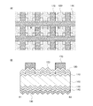
図1(A)は、本発明の一態様における光電変換装置の平面図であり、図1(B)は、該平面図の線分A1−A2における断面図である。該光電変換装置は、結晶性シリコン基板100、該結晶性シリコン基板の一方の面上に形成された第1のシリコン半導体層110、第2のシリコン半導体層120、透光性導電膜150、および第1の電極170、並びに、該結晶性シリコン基板の他方の面上に形成された第3のシリコン半導体層130、第4のシリコン半導体層140、および第2の電極190を含んで構成される。なお、第1の電極170はグリッド電極であり、第1の電極170側が受光面となる。
FIG. 1A is a plan view of a photoelectric conversion device according to one embodiment of the present invention, and FIG. 1B is a cross-sectional view taken along line A1-A2 in the plan view. The photoelectric conversion device includes a
なお、図1(A)の平面図に示す第1の電極170の形状は一例であり、それに限らない。例えば、縦、横の各電極の一方をバスバー電極、他方をフィンガー電極として作用させるために、縦、横の各電極の幅、本数、間隔を実施者が任意に設定することができる。また、図5に示すように、第1の電極170と第2のシリコン半導体層120が重なる領域を少なくして、受光領域を拡大する構成としてもよい。
Note that the shape of the
また、図1(B)では、結晶性シリコン基板100の表裏に凹凸加工を施した例を示している。凹凸加工された面では入射光が多重反射し、光電変換領域内には光が斜めに進行することから光路長を増大させることができる。また、裏面反射光が表面で全反射する、所謂光閉じ込め効果を起こさせることもできる。なお、第1の電極170の広幅化や断線を防ぐために、第1のシリコン半導体層110が接する結晶性シリコン基板100の一領域は、凹凸加工をせずに平坦な領域としてもよい。
Further, FIG. 1B shows an example in which unevenness processing is performed on the front and back of the
結晶性シリコン基板100には一導電型を有する単結晶シリコン基板、または多結晶シリコン基板を用いることができる。本実施の形態においては、結晶性シリコン基板100にはn型の導電型を有する単結晶シリコン基板が用いられる。
As the
上記構造において、結晶性シリコン基板100の一方の面上に形成される第1のシリコン半導体層110および開口部を有する第2のシリコン半導体層120には、p型のシリコン半導体層を用いることができる。該p型シリコン半導体層には、例えば、ホウ素、アルミニウム、またはガリウムなどのp型の導電型を付与する不純物、および水素を含むシリコン半導体層を用いることができる。
In the above structure, a p-type silicon semiconductor layer is used for the first
なお、第1のシリコン半導体層110には、第2のシリコン半導体層120よりもキャリア濃度が低いシリコン半導体層を用いることができる。このような構成を明瞭化するため、本明細書においては、第1のシリコン半導体層110などの相対的にキャリア濃度の低いp型半導体層の導電型をp−型と呼称するのに対し、第2のシリコン半導体層120などの相対的にキャリア濃度の高いp型半導体層の導電型をp+型と呼称する。
Note that a silicon semiconductor layer having a carrier concentration lower than that of the second
なお、半導体層のキャリア濃度を調整するには、プラズマCVD法等による成膜時にドーパントガスの流量比率を変化させれば良い。原料ガス(例えば、モノシランなど)に対して、ドーパントガス(例えば、ジボラン、ホスフィンなど)の流量比率を高くするほどキャリア濃度を高くすることができる。または、成膜圧力、温度、電力密度などを変化させることにより、形成された半導体層中の不純物の活性化率を変化させてキャリア濃度を調整することもできる。 Note that in order to adjust the carrier concentration of the semiconductor layer, the flow rate ratio of the dopant gas may be changed during film formation by a plasma CVD method or the like. The carrier concentration can be increased as the flow rate ratio of the dopant gas (for example, diborane, phosphine) to the source gas (for example, monosilane) is increased. Alternatively, the carrier concentration can be adjusted by changing the activation rate of impurities in the formed semiconductor layer by changing the deposition pressure, temperature, power density, and the like.
なお、本発明の一態様におけるp−型シリコン半導体層には、不純物による局在準位の少ない非晶質シリコン半導体層を用いることが好ましい。該非晶質シリコン半導体層の電気伝導度は、暗状態で1×10⁻¹⁰S/cm〜1×10−5S/cm、好ましくは1×10−9S/cm〜1×10−6S/cm、さらに好ましくは1×10−9S/cm〜1×10−7S/cmである。 Note that an amorphous silicon semiconductor layer with few localized levels due to impurities is preferably used for the p − -type silicon semiconductor layer in one embodiment of the present invention. The electric conductivity of the amorphous silicon semiconductor layer is 1 × 10 −10 S / cm to 1 × 10 −5 S / cm, preferably 1 × 10 −9 S / cm to 1 × 10 −6 S in the dark state. / Cm, more preferably 1 × 10 −9 S / cm to 1 × 10 −7 S / cm.
なお、上記電気伝導度(暗伝導度)を有する非晶質シリコン半導体層は、p型の導電型を付与する不純物を故意に添加することによってp−型に制御された非晶質シリコン半導体層である。 The amorphous silicon semiconductor layer having the electrical conductivity (dark conductivity) is an amorphous silicon semiconductor layer controlled to be p − type by intentionally adding an impurity imparting p type conductivity. It is.
また、本発明の一態様におけるp+型シリコン半導体層の電気伝導度は、暗状態で1×10⁻⁵S/cmより大きいことが好ましい。 In addition, the electrical conductivity of the p + type silicon semiconductor layer in one embodiment of the present invention is preferably larger than 1 × 10 −5 S / cm in the dark state.
p−n接合を用いた光電変換装置では、p−n接合内の電界を高め、拡散電位を高めることが電気特性を向上させる一つの手段となる。一般的にはキャリア濃度の高いp+型半導体またはn+型半導体を用いて接合を形成することで拡散電位を高めることができるが、p+型半導体およびn+型半導体は導電型を付与する不純物を多く含み、該不純物は局在準位を増加させてしまう。また、該局在準位によって界面準位の生成が進み、接合部近傍でキャリアの再結合が誘発されてしまう。したがって、接合層のキャリア濃度を高めるだけでは、光電変換装置の電気特性の向上は見込めない。 In a photoelectric conversion device using a pn junction, increasing the electric field in the pn junction and increasing the diffusion potential is one means for improving electrical characteristics. In general, a diffusion potential can be increased by forming a junction using a p + type semiconductor or an n + type semiconductor having a high carrier concentration. However, the p + type semiconductor and the n + type semiconductor impart conductivity type. It contains a lot of impurities, and the impurities increase the localized level. In addition, the generation of interface states is advanced by the localized states, and carrier recombination is induced in the vicinity of the junction. Therefore, the electrical characteristics of the photoelectric conversion device cannot be improved only by increasing the carrier concentration of the bonding layer.
一方、本発明の一態様における光電変換装置では、結晶性シリコン基板100の一方の面において、p−型シリコン半導体層と、p+型シリコン半導体層を積層した構成となっている。該p−型シリコン半導体層は、水素を含む欠陥の少ない半導体層であり、結晶性シリコン基板表面の欠陥を終端するパッシベーション層として作用すると同時に、拡散電位を形成する接合層として寄与する。また、該p+型シリコン半導体層は、さらに拡散電位を高めるように作用する。このような緩やかな接合(n−p−−p+)が形成される構造により、拡散電位を高めながらも界面準位の影響によるキャリアの再結合を極力抑えることができる。
On the other hand, the photoelectric conversion device according to one embodiment of the present invention has a structure in which a p − type silicon semiconductor layer and a p + type silicon semiconductor layer are stacked on one surface of the
また、本発明の一態様である光電変換装置では、第2のシリコン半導体層120に開口部が設けられている。したがって、該開口部においては、第2のシリコン半導体層120を介さずに光電変換領域である結晶性シリコン基板へ光の照射をさせることができる。従来のヘテロ接合型光電変換装置では、界面欠陥を低減させるためのパッシベーション層と拡散電位を高めるための接合層の双方が光電変換領域の全面に積層されていたため、光吸収損失が顕著であった。一方で、本発明の一態様である光電変換装置では、該開口部において、接合層に相当する第2のシリコン半導体層120による光吸収がないため、光吸収損失を極めて少なくすることができる。この効果により、特に光電変換装置の短絡電流を向上させることができる。
In the photoelectric conversion device which is one embodiment of the present invention, the second
また、本発明の一態様である光電変換装置は、図2(A)に示す平面図、および図2(B)に示す該平面図の線分B1−B2における断面図の構成を有していてもよい。該光電変換装置は、図1(A)、(B)に示す光電変換装置とは第2のシリコン半導体層120の開口部を少なくした点で異なり、その他の構成は同じである。なお、第2のシリコン半導体層120の開口形状や開口面積は図示した例に限らず、自由に設定することができる。
In addition, the photoelectric conversion device which is one embodiment of the present invention has a structure of a plan view shown in FIG. 2A and a cross-sectional view taken along line B1-B2 of the plan view shown in FIG. May be. The photoelectric conversion device is different from the photoelectric conversion device shown in FIGS. 1A and 1B in that the number of openings in the second
なお、図2(A)の平面図に示す第1の電極170の形状は一例であり、それに限らない。例えば、縦、横の各電極の一方をバスバー電極、他方をフィンガー電極として作用させるために、縦、横の各電極の幅、本数、間隔を実施者が任意に設定することができる。また、図6に示すように、第1の電極170と第2のシリコン半導体層120が重なる領域を少なくして、受光領域を拡大する構成としてもよい。
Note that the shape of the
このような構成とすることで、拡散電位をさらに高めることができ、開放電圧および曲線因子を向上させることができる。なお、図2(A)、(B)に示す光電変換装置では、一部の第2のシリコン半導体層120で光吸収が起こるため、図1(A)、(B)に示す光電変換装置よりも短絡電流は小さくなる。したがって、両者の構成の選択は、実施者が用途に応じて適宜選択すればよい。 With such a configuration, the diffusion potential can be further increased, and the open circuit voltage and the fill factor can be improved. Note that in the photoelectric conversion devices illustrated in FIGS. 2A and 2B, light absorption occurs in some of the second silicon semiconductor layers 120, so that the photoelectric conversion devices illustrated in FIGS. However, the short circuit current becomes smaller. Therefore, the practitioner may select the both configurations as appropriate according to the application.
結晶性シリコン基板100の他方の面上に形成される第3のシリコン半導体層130および第4のシリコン半導体層140には、n型のシリコン半導体層を用いることができる。該n型半導体層には、例えば、リン、ヒ素、またはアンチモンなどのn型の導電型を付与する不純物、および水素を含むシリコン半導体層を用いることができる。
An n-type silicon semiconductor layer can be used for the third
なお、第3のシリコン半導体層130には、第4のシリコン半導体層140よりもキャリア濃度が低いシリコン半導体層を用いることができる。このような構成を明瞭化するため、本明細書においては、第3のシリコン半導体層130などの相対的にキャリア濃度の低いn型半導体層の導電型をn−型と呼称するのに対し、第4のシリコン半導体層140などの相対的にキャリア濃度の高いn型半導体層の導電型をn+型と呼称する。
Note that a silicon semiconductor layer having a carrier concentration lower than that of the fourth
なお、本発明の一態様におけるn−型シリコン半導体層には、不純物による局在準位の少ない非晶質シリコン半導体層を用いることが好ましい。該非晶質シリコン半導体層は、水素を含む欠陥の少ない半導体層であり、結晶性シリコン基板100の表面欠陥を終端するパッシベーション層として作用させることができる。該非晶質シリコン半導体層の電気伝導度は、暗状態で1×10⁻⁹S/cm〜1×10−4S/cm、好ましくは1×10−8S/cm〜1×10−5S/cm、さらに好ましくは1×10−8S/cm〜1×10−6S/cmである。
Note that as the n − -type silicon semiconductor layer in one embodiment of the present invention, an amorphous silicon semiconductor layer with few localized levels due to impurities is preferably used. The amorphous silicon semiconductor layer is a semiconductor layer containing few defects containing hydrogen and can serve as a passivation layer for terminating surface defects of the
なお、上記電気伝導度(暗伝導度)を有する非晶質シリコン半導体層は、n型の導電型を付与する不純物を故意に添加することによってn−型に制御された非晶質シリコン半導体層である。 The amorphous silicon semiconductor layer having the electrical conductivity (dark conductivity) is an amorphous silicon semiconductor layer controlled to be n − type by intentionally adding an impurity imparting n-type conductivity. It is.
また、本発明の一態様におけるn+型シリコン半導体層の電気伝導度は、暗状態で1×10⁻⁴S/cmより大きいことが好ましい。 In addition, the electrical conductivity of the n + -type silicon semiconductor layer in one embodiment of the present invention is preferably larger than 1 × 10 −4 S / cm in the dark state.
また、n+型シリコン半導体層である第4のシリコン半導体層140と結晶性シリコン基板100との間には、第3のシリコン半導体層130を介してn−n+接合が形成される。つまり、第4のシリコン半導体層140は、BSF(Back Surface Field)層として作用する。該接合により形成される電界により少数キャリアがp−n接合側にはね返されることから、第2の電極190近傍でのキャリアの再結合を防止することができる。
In addition, an n−n + junction is formed between the fourth
なお、本発明の一態様における光電変換装置においては、第3のシリコン半導体層130がi型であってもよい。本実施の形態においてi型の半導体層とは、p型もしくはn型を付与する不純物を故意に添加しない高抵抗半導体層、または、p型もしくはn型を付与する不純物を故意に添加することによって導電型が調整された高抵抗半導体層であって、上述したp−型シリコン半導体層およびn−型シリコン半導体層よりも小さい値の電気伝導度(暗伝導度)を有する実質i型の半導体層を意味する。
Note that in the photoelectric conversion device according to one embodiment of the present invention, the third
透光性導電膜150には、例えば、インジウム錫酸化物、珪素を含むインジウム錫酸化物、亜鉛を含む酸化インジウム、酸化亜鉛、ガリウムを含む酸化亜鉛、アルミニウムを含む酸化亜鉛、酸化錫、フッ素を含む酸化錫、アンチモンを含む酸化錫、またはグラフェン等を用いることができる。また、透光性導電膜は単層に限らず、異なる膜の積層でも良い。
The light-transmitting
また、第1の電極170および第2の電極190には、銀、アルミニウム、銅などの低抵抗金属を用いることができ、スパッタ法や真空蒸着法などで形成することができる。または、スクリーン印刷法やインクジェット法を用いて、銀ペーストや、銅ペーストなどの導電性樹脂で形成しても良い。
The
なお、本発明の一態様における光電変換装置は、図3(A)、(B)に例示するように、表裏のどちらか一方のみに凹凸加工を施した構成であっても良い。両面が凹凸加工された光電変換装置では、光路長増大などの光学的効果が得られる一方で、結晶性シリコン基板の表面積が増大するため、表面欠陥の絶対量も増大してしまう。したがって、光学的効果と表面欠陥量のバランスを考慮し、より良好な電気特性が得られるように実施者が構造を決定すればよい。 Note that the photoelectric conversion device according to one embodiment of the present invention may have a structure in which uneven processing is performed on only one of the front and back sides as illustrated in FIGS. In the photoelectric conversion device whose both surfaces are processed to be uneven, an optical effect such as an increase in the optical path length can be obtained, but the surface area of the crystalline silicon substrate is increased, so that the absolute amount of surface defects is also increased. Therefore, in consideration of the balance between the optical effect and the amount of surface defects, the practitioner may determine the structure so as to obtain better electrical characteristics.
また、本発明の一態様における光電変換装置は、図4(A)、(B)に例示するように、第3のシリコン半導体層上に開口部を有する第4のシリコン半導体層140を形成し、該第4のシリコン半導体層上に透光性導電膜180を形成し、該透光性導電膜上にグリッド形状の第2の電極190を形成して、両面を受光面とする構造としてもよい。
In the photoelectric conversion device of one embodiment of the present invention, as illustrated in FIGS. 4A and 4B, the fourth
次に、図1(A)、(B)に示した光電変換装置の作製方法について、図7および図8を用いて説明する。 Next, a method for manufacturing the photoelectric conversion device illustrated in FIGS. 1A and 1B will be described with reference to FIGS.
本発明の一態様に用いることのできる結晶性シリコン基板100には、n型の導電型を有する単結晶シリコン基板や多結晶シリコン基板を用いることができる。これらの結晶性シリコン基板の製造方法は、特に限定されない。本実施の形態においては、結晶性シリコン基板100にMCZ(Magnetic Czochralski)法で製造された(100)面を表面に有する単結晶シリコン基板を用いる。
As the
次に、結晶性シリコン基板100の表裏に凹凸加工を行う(図7(A)参照)。なお、ここでは上述したように(100)面を表面に有する単結晶シリコン基板を用いる場合を例として凹凸加工の方法の一例を説明する。結晶性シリコン基板100として多結晶シリコン基板を用いる場合は、ドライエッチング法などを用いて凹凸加工を行えばよい。
Next, uneven processing is performed on the front and back of the crystalline silicon substrate 100 (see FIG. 7A). Note that, as described above, an example of a method for processing the unevenness will be described by using a single crystal silicon substrate having a (100) plane as an example. When a polycrystalline silicon substrate is used as the
初期の単結晶シリコン基板がスライス加工のみである基板の場合は、単結晶シリコン基板の表面から10〜20μmに残留するダメージ層をウエットエッチング工程にて取り除く。エッチング液には、比較的高濃度のアルカリ溶液、例えば、10〜50%の水酸化ナトリウム水溶液、または同濃度の水酸化カリウム水溶液を用いることができる。または、フッ酸と硝酸を混合した混酸や、それらに酢酸を混合した混酸を用いても良い。 In the case where the initial single crystal silicon substrate is a substrate that only undergoes slicing, the damaged layer remaining at 10 to 20 μm from the surface of the single crystal silicon substrate is removed by a wet etching process. As the etching solution, a relatively high concentration alkaline solution, for example, a 10 to 50% sodium hydroxide aqueous solution or a potassium hydroxide aqueous solution having the same concentration can be used. Alternatively, a mixed acid in which hydrofluoric acid and nitric acid are mixed, or a mixed acid in which acetic acid is mixed with them may be used.
次に、ダメージ層除去後の単結晶シリコン基板表面に付着している不純物を酸洗浄で取り除く。酸としては、例えば、0.5%フッ酸と1%過酸化水素水の混合液(FPM)などを用いることができる。またはRCA洗浄などを行っても良い。なお、この酸洗浄工程は省いても良い。 Next, the impurities adhering to the surface of the single crystal silicon substrate after removing the damaged layer are removed by acid cleaning. As the acid, for example, a mixed solution (FPM) of 0.5% hydrofluoric acid and 1% hydrogen peroxide water can be used. Alternatively, RCA cleaning or the like may be performed. This acid cleaning step may be omitted.
凹凸は、結晶シリコンのアルカリ溶液によるエッチングにおいて、面方位に対するエッチングレートの違いを利用して形成する。エッチング液には比較的低濃度のアルカリ溶液、例えば、1〜5%の水酸化ナトリウム水溶液、または同濃度の水酸化カリウム水溶液を用いることができ、好ましくは、数%のイソプロピルアルコールを添加する。エッチング液の温度は70〜90℃とし、30〜60分間、単結晶シリコン基板をエッチング液に浸漬する。この処理により、単結晶シリコン基板表面に、微細な略四角錐状の複数の凸部、および隣接する凸部間で構成される凹部からなる凹凸を形成することができる。 The unevenness is formed by utilizing the difference in etching rate with respect to the plane orientation in etching with an alkaline solution of crystalline silicon. As the etching solution, an alkaline solution having a relatively low concentration, for example, a 1 to 5% sodium hydroxide aqueous solution or a potassium hydroxide aqueous solution having the same concentration can be used. Preferably, several percent isopropyl alcohol is added. The temperature of the etching solution is 70 to 90 ° C., and the single crystal silicon substrate is immersed in the etching solution for 30 to 60 minutes. By this treatment, the surface of the single crystal silicon substrate can be formed with irregularities including a plurality of fine convex portions having a substantially quadrangular pyramid shape and concave portions formed between adjacent convex portions.
次に、上述の凹凸を形成するためのエッチング工程では、シリコンの表層に不均一な酸化層が形成されるため、該酸化層を取り除く。また、該酸化層にはアルカリ溶液の成分が残存しやすいため、それを取り除く目的もある。アルカリ金属、例えばNaイオンやKイオンがシリコン中に侵入するとライフタイムが劣化するため、光電変換装置の電気特性が著しく低下してしまう。なお、この酸化層を除去するには、1〜5%の希フッ酸を用いれば良い。 Next, in the etching process for forming the unevenness described above, a non-uniform oxide layer is formed on the surface layer of silicon, and therefore the oxide layer is removed. Moreover, since the components of the alkaline solution are likely to remain in the oxide layer, there is also an object to remove them. When an alkali metal such as Na ion or K ion enters silicon, the lifetime is deteriorated, so that the electrical characteristics of the photoelectric conversion device are remarkably deteriorated. In order to remove the oxide layer, 1 to 5% dilute hydrofluoric acid may be used.
次に、フッ酸と硝酸を混合した混酸、または、それらに酢酸を混合した混酸を用いて単結晶シリコン基板の表面をエッチングし、金属成分などの不純物を除去することが好ましい。酢酸を混合することで、硝酸の酸化力を維持し、エッチング工程を安定にする効果、およびエッチングレートを調整する効果が得られる。例えば、各酸の体積比率は、フッ酸:硝酸:酢酸=1:(1.5〜3):(2〜4)とすることができる。なお、本明細書では、フッ酸、硝酸および酢酸の混酸液をフッ硝酢酸と呼ぶ。また、このフッ硝酢酸を用いたエッチング工程では、凸部の頂点の断面における角度を大きくする方向に変化させることから、表面積が低減し、表面欠陥の絶対量を低減することができる。なお、このフッ硝酢酸を用いたエッチングを行う場合は、上述の希フッ酸を用いた酸化層の除去工程を省くこともできる。ここまでの工程により、結晶性シリコン基板100である単結晶シリコン基板の表面に凹凸を形成することができる。
Next, it is preferable to remove impurities such as metal components by etching the surface of the single crystal silicon substrate using a mixed acid obtained by mixing hydrofluoric acid and nitric acid, or a mixed acid obtained by mixing acetic acid with the mixed acid. By mixing acetic acid, it is possible to maintain the oxidizing power of nitric acid, stabilize the etching process, and adjust the etching rate. For example, the volume ratio of each acid may be hydrofluoric acid: nitric acid: acetic acid = 1: (1.5-3) :( 2-4). In the present specification, a mixed acid solution of hydrofluoric acid, nitric acid and acetic acid is referred to as fluorinated acetic acid. Further, in the etching process using this fluorinated acetic acid, the angle in the cross section at the apex of the convex portion is changed in the increasing direction, so that the surface area can be reduced and the absolute amount of surface defects can be reduced. Note that in the case of performing etching using this fluorinated acetic acid, the step of removing the oxide layer using dilute hydrofluoric acid can be omitted. Through the steps so far, unevenness can be formed on the surface of the single crystal silicon substrate which is the
なお、図3(A)、(B)に示すような、結晶性シリコン基板100の片面のみに凹凸加工を行うには、上記凹凸加工工程を行う前に、結晶性シリコン基板100の一方の面にアルカリ耐性および酸耐性の強い樹脂膜などを設け、上記凹凸加工工程後に該樹脂膜を取り除けばよい。
Note that, in order to perform uneven processing on only one surface of the
次いで、水洗などの適切な洗浄の後、受光面とは逆側となる結晶性シリコン基板100の面上にプラズマCVD法を用いて第3のシリコン半導体層130を形成する。第3のシリコン半導体層130の厚さは、3nm以上50nm以下とすることが好ましい。本実施の形態において、第3のシリコン半導体層130はn−型の非晶質シリコンであり、膜厚は5nmとする。
Next, after appropriate cleaning such as rinsing, a third
第3のシリコン半導体層130の成膜条件としては、例えば、反応室にモノシラン:水素ベースのホスフィン(0.5%)=1:(0.3〜1未満)となる流量比率で原料ガスを導入し、反応室内の圧力を100Pa以上200Pa以下、電極間隔を10mm以上40mm以下、カソード電極の面積を基準とする電力密度を8mW/cm2以上120mW/cm2以下、基板温度を150℃以上300℃以下とすればよい。
As a film formation condition of the third
次に、第3のシリコン半導体層130上に第4のシリコン半導体層140を形成する(図3(B)参照)。第4のシリコン半導体層140の厚さは3nm以上50nm以下とすることが好ましい。本実施の形態において、第4のシリコン半導体層140はn+型の非晶質シリコンであり、膜厚は10nmとする。
Next, a fourth
第4のシリコン半導体層140の成膜条件は、例えば、反応室にモノシラン:水素ベースのホスフィン(0.5%)=1:(1〜15)となる流量比率で原料ガスを導入し、反応室内の圧力を100Pa以上200Pa以下とし、電極間隔を10mm以上40mm以下とし、カソード電極の面積を基準とする電力密度を8mW/cm2以上120mW/cm2以下、基板温度を150℃以上300℃以下とすればよい。
For example, the fourth
次に、受光面側となる結晶性シリコン基板100の面上にプラズマCVD法を用いて第1のシリコン半導体層110を形成する(図7(B)参照)。第1のシリコン半導体層110の厚さは、3nm以上50nm以下とすることが好ましく、本実施の形態において、第1のシリコン半導体層110はp−型の非晶質シリコンであり、膜厚は5nmとする。
Next, a first
第1のシリコン半導体層110の成膜条件としては、例えば、反応室にモノシラン:水素ベースのジボラン(0.1%)=1:(0.01〜1未満)となる流量比率で原料ガスを導入し、反応室内の圧力を100Pa以上200Pa以下、電極間隔を10mm以上40mm以下、カソード電極の面積を基準とする電力密度を8mW/cm2以上120mW/cm2以下、基板温度を150℃以上300℃以下とすればよい。
As a film formation condition of the first
次に、第1のシリコン半導体層110上に開口部を有するマスク200を形成する。第2のシリコン半導体層120は該マスクを利用して、リフトオフ法により形成する。該マスクには、フォトレジストや酸化シリコンなどの無機材料で形成することが好ましい。本実施の形態では、スパッタ法などの成膜方法を用いて酸化シリコン層を形成し、フォトリソグラフィ法、エッチング法などの公知の方法を用いて、マスク200を形成する(図7(C)参照)。
Next, a
次に、マスク200および第1のシリコン半導体層110上にp型の導電型を有するシリコン半導体膜120aを形成する(図8(A)参照)。シリコン半導体膜120aの厚さは3nm以上50nm以下とすることが好ましい。本実施の形態において、シリコン半導体膜120aはp+型の非晶質シリコンであり、膜厚は10nmとする。
Next, a
シリコン半導体膜120aの成膜条件は、例えば、反応室にモノシラン:水素ベースのジボラン(0.1%)=1:(1〜20)となる流量比率で原料ガスを導入し、反応室内の圧力を100Pa以上200Pa以下とし、電極間隔を8mm以上40mm以下とし、カソード電極の面積を基準とする電力密度を8mW/cm2以上50mW/cm2以下、基板温度を150℃以上300℃以下とすればよい。
The deposition conditions of the
次に、希フッ酸、またはフッ酸とフッ化アンモニウムの混合液であるバッファードフッ酸を用いて、マスク200および余分なシリコン半導体膜120aを同時に除去して、第2のシリコン半導体層120を形成する(図8(B)参照)。
Next, the
なお、本実施の形態において、第1のシリコン半導体層110、第2のシリコン半導体層120、第3のシリコン半導体層130、および第4のシリコン半導体層140の成膜に用いる電源には周波数13.56MHzのRF電源を用いるが、27.12MHz、60MHz、または100MHzのRF電源を用いても良い。また、連続放電だけでなく、パルス放電にて成膜を行っても良い。パルス放電を行うことで、膜質の向上や気相中で発生するパーティクルを低減することができる。
Note that in this embodiment mode, the power supply used for forming the first
また、結晶性シリコン基板100の表裏に設ける膜の形成順序は、上記の方法に限らず、図8(B)に示した構造が形成できればよい。例えば、第3のシリコン半導体層130を形成し、その次に第1のシリコン半導体層110を形成してもよい。
Further, the order of forming the films provided on the front and back sides of the
次に、第2のシリコン半導体層120上に透光性導電膜150を形成する。該透光性導電膜は、前述の材料を例えばスパッタ法などを用いて成膜することができる。膜厚は10nm以上1000nm以下とすることが好ましい。
Next, a light-transmitting
次に、第4のシリコン半導体層140上に第2の電極190を形成する。第2の電極190には、銀、アルミニウム、銅などの低抵抗金属を用いることができ、スパッタ法や真空蒸着法などで形成することができる。または、スクリーン印刷法やインクジェット法を用いて、銀ペーストや、銅ペーストなどの導電性樹脂で形成しても良い。
Next, the
次に、透光性導電膜150上に、第2のシリコン半導体層120と重なるように第1の電極170を形成する(図8(C)参照)。第1の電極170はグリッド電極であり、銀ペースト、銅ペースト、ニッケルペースト、モリブデンペーストなどの導電性樹脂を用いて、スクリーン印刷法やインクジェット法で形成することが好ましい。また、第1の電極170は、銀ペーストと銅ペーストを積層するなど、異なる材料の積層であっても良い。
Next, the
なお、図2(A)、(B)に示した光電変換装置を作製するには、第1の電極170と第2のシリコン半導体層120の一部とが重なるように、それぞれの形状を異ならせて形成すればよい。
Note that in order to manufacture the photoelectric conversion device illustrated in FIGS. 2A and 2B, the shapes of the
また、図4(A)、(B)の構成の光電変換装置を形成するには、第3のシリコン半導体層130を形成した後に、図7(C)〜図8(C)に示す第2のシリコン半導体層120、透光性導電膜150、第1の電極170の形成方法に従って、第4のシリコン半導体層140、透光性導電膜180、第2の電極190を形成すればよい。
4A and 4B, the second silicon shown in FIGS. 7C to 8C is formed after the third
以上により、本発明の一態様である光吸収損失および抵抗損失の少ない光電変換装置を作製することができる。 Through the above, a photoelectric conversion device which is one embodiment of the present invention and has low light absorption loss and resistance loss can be manufactured.
本実施の形態は、他の実施の形態と自由に組み合わすことができる。 This embodiment can be freely combined with any of the other embodiments.
(実施の形態2)
本実施の形態では、実施の形態1で示した光電変換装置とは異なる構成の光電変換装置について説明する。なお、実施の形態1と共通する点については、本実施の形態ではその詳細な説明は省略する。
(Embodiment 2)
In this embodiment, a photoelectric conversion device having a structure different from that of the photoelectric conversion device described in Embodiment 1 will be described. Note that the points common to the first embodiment are not described in detail in this embodiment.
図9は、本発明の一態様における光電変換装置の断面図である。該光電変換装置は、表面が凹凸加工された結晶性シリコン基板300、該結晶性シリコン基板の一方の面上に形成された第1のシリコン半導体層310、該第1のシリコン半導体層上に形成された開口部を有する第1の透光性導電膜410、該開口部に形成された第2のシリコン半導体層320、該第2のシリコン半導体層上に形成された第1の電極370、および該結晶性シリコン基板の一方の面上に形成された上記積層膜を覆う第2の透光性導電膜420を含む。また、該光電変換装置は、該結晶性シリコン基板の他方の面上に形成された第3のシリコン半導体層330、該第3のシリコン半導体層に形成された第4のシリコン半導体層340、該第4のシリコン半導体層上に形成された第2の電極390を含む。なお、第1の電極370はグリッド電極であり、第1の電極370側が受光面となる。
FIG. 9 is a cross-sectional view of a photoelectric conversion device according to one embodiment of the present invention. The photoelectric conversion device is formed on a
また、図10(A)に示すように、表裏のどちらか一方のみに凹凸加工を施した構成であっても良い。なお、第1の電極370の広幅化や断線を防ぐために、第1のシリコン半導体層310が接する結晶性シリコン基板300の一領域は、凹凸加工をせずに平坦な領域としてもよい。
Moreover, as shown to FIG. 10 (A), the structure which gave the uneven | corrugated process to either one of front and back may be sufficient. Note that in order to prevent the
また、図10(B)に示すように、第3のシリコン半導体層330上に開口部を有する第3の透光性導電膜430を形成し、該開口部に第4のシリコン半導体層340を形成し、該第4のシリコン半導体層上に第2の電極390を形成し、該結晶性シリコン基板の他方の面上に形成された上記積層膜を覆う第4の透光性導電膜440を形成して、両面を受光面とする構造としてもよい。
As shown in FIG. 10B, a third light-transmitting
上記構造において、結晶性シリコン基板300の一方の面上に形成される第1のシリコン半導体層310および第2のシリコン半導体層320には、p型のシリコン半導体層を用いることができる。該p型半導体層には、例えば、ホウ素、アルミニウム、またはガリウムなどのp型の導電型を付与する不純物、および水素を含むシリコン半導体層を用いることができる。
In the above structure, a p-type silicon semiconductor layer can be used for the first
なお、第1のシリコン半導体層310には、第2のシリコン半導体層320よりもキャリア濃度が低いシリコン半導体層を用いることができる。すなわち、第1のシリコン半導体層310にはp−型、第2のシリコン半導体層320にはp+型の導電型を有するシリコン半導体層を用いることができる。
Note that a silicon semiconductor layer whose carrier concentration is lower than that of the second
なお、本発明の一態様におけるp−型シリコン半導体層には、不純物による局在準位の少ない非晶質シリコン半導体層を用いることが好ましい。該非晶質シリコン半導体層の電気伝導度は、暗状態で1×10⁻¹⁰S/cm〜1×10−5S/cm、好ましくは1×10−9S/cm〜1×10−6S/cm、さらに好ましくは1×10−9S/cm〜1×10−7S/cmである。 Note that an amorphous silicon semiconductor layer with few localized levels due to impurities is preferably used for the p − -type silicon semiconductor layer in one embodiment of the present invention. The electric conductivity of the amorphous silicon semiconductor layer is 1 × 10 −10 S / cm to 1 × 10 −5 S / cm, preferably 1 × 10 −9 S / cm to 1 × 10 −6 S in the dark state. / Cm, more preferably 1 × 10 −9 S / cm to 1 × 10 −7 S / cm.
また、本発明の一態様におけるp+型シリコン半導体層の電気伝導度は、暗状態で1×10⁻⁵S/cmより大きいことが好ましい。 In addition, the electrical conductivity of the p + type silicon semiconductor layer in one embodiment of the present invention is preferably larger than 1 × 10 −5 S / cm in the dark state.
また、結晶性シリコン基板100の他方の面上に形成される第3のシリコン半導体層330および第4のシリコン半導体層340には、n型のシリコン半導体層を用いることができる。該n型シリコン半導体層には、例えば、リン、ヒ素、またはアンチモンなどのn型の導電型を付与する不純物、および水素を含むシリコン半導体層を用いることができる。
An n-type silicon semiconductor layer can be used as the third
なお、第3のシリコン半導体層330には、第4のシリコン半導体層340よりもキャリア濃度が低いシリコン半導体層を用いることができる。すなわち、第3のシリコン半導体層330にはn−型、第4のシリコン半導体層340にはn+型の導電型を有するシリコン半導体層を用いることができる。
Note that a silicon semiconductor layer having a carrier concentration lower than that of the fourth
なお、本発明の一態様におけるn−型シリコン半導体層には、不純物による局在準位の少ない非晶質シリコン半導体層を用いることが好ましい。該非晶質シリコン半導体層の電気伝導度は、暗状態で1×10⁻⁹S/cm〜1×10−4S/cm、好ましくは1×10−9S/cm〜1×10−5S/cm、さらに好ましくは1×10−9S/cm〜1×10−6S/cmである。 Note that as the n − -type silicon semiconductor layer in one embodiment of the present invention, an amorphous silicon semiconductor layer with few localized levels due to impurities is preferably used. The electric conductivity of the amorphous silicon semiconductor layer is 1 × 10 −9 S / cm to 1 × 10 −4 S / cm, preferably 1 × 10 −9 S / cm to 1 × 10 −5 S in the dark state. / Cm, more preferably 1 × 10 −9 S / cm to 1 × 10 −6 S / cm.
また、本発明の一態様におけるn+型シリコン半導体層の電気伝導度は、暗状態で1×10⁻⁴S/cmより大きいことが好ましい。 In addition, the electrical conductivity of the n + -type silicon semiconductor layer in one embodiment of the present invention is preferably larger than 1 × 10 −4 S / cm in the dark state.
第1乃至第4の透光性導電膜410、420、430、440には、例えば、インジウム錫酸化物、珪素を含むインジウム錫酸化物、亜鉛を含む酸化インジウム、酸化亜鉛、ガリウムを含む酸化亜鉛、アルミニウムを含む酸化亜鉛、酸化錫、フッ素を含む酸化錫、アンチモンを含む酸化錫、またはグラフェン等を用いることができる。また、透光性導電膜は単層に限らず、異なる膜の積層でも良い。
The first to fourth light-transmitting
また、第1の電極370および第2の電極390には、銀、アルミニウム、銅などの低抵抗金属を用いることができ、スパッタ法や真空蒸着法などで形成することができる。または、スクリーン印刷法やインクジェット法を用いて、銀ペーストや、銅ペーストなどの導電性樹脂で形成しても良い。
The
以上の構成を有する本実施の形態における光電変換装置は、実施の形態1で説明した光電変換装置と同様に緩やかな接合(n−p−−p+)が形成される構造であり、拡散電位を高めながらも界面準位の影響によるキャリアの再結合を極力抑えることができる。したがって、特に開放電圧、および曲線因子を向上させることができる。 The photoelectric conversion device in this embodiment having the above structure has a structure in which a loose junction (np − −p + ) is formed as in the photoelectric conversion device described in Embodiment 1, and has a diffusion potential. The carrier recombination due to the influence of the interface state can be suppressed as much as possible while increasing the. Therefore, particularly the open circuit voltage and the fill factor can be improved.
また、本実施の形態における光電変換装置では、第2のシリコン半導体層320に開口部が形成されており、該開口部においては、第2のシリコン半導体層320による光吸収がないため、光吸収損失を極めて少なくすることができる。
In the photoelectric conversion device in this embodiment, an opening is formed in the second
次に、図9に示した光電変換装置の作製方法について、図11および図12を用いて説明する。 Next, a method for manufacturing the photoelectric conversion device illustrated in FIG. 9 is described with reference to FIGS.
本発明の一態様に用いることのできる結晶性シリコン基板300には、n型の導電型を有する単結晶シリコン基板や多結晶シリコン基板を用いることができる。
As the
次に、実施の形態1の図7(A)を説明する方法に従って、結晶性シリコン基板300の表裏に凹凸加工を行う(図11(A)参照)。 Next, in accordance with the method described in Embodiment 1 with reference to FIG. 7A, uneven processing is performed on the front and back of the crystalline silicon substrate 300 (see FIG. 11A).
次に、受光面とは逆側となる結晶性シリコン基板300の面上にプラズマCVD法を用いて第3のシリコン半導体層330を形成する。第3のシリコン半導体層330の厚さは、3nm以上50nm以下とすることが好ましい。本実施の形態において、第3のシリコン半導体層330はn−型の非晶質シリコンであり、膜厚は5nmとする。
Next, a third
第3のシリコン半導体層330の成膜条件としては、実施の形態1で説明した第3のシリコン半導体層130の成膜条件を参照することができる。
As the film formation condition of the third
次に、第3のシリコン半導体層330上に第4のシリコン半導体層340を形成する。第4のシリコン半導体層340の厚さは3nm以上50nm以下とすることが好ましい。本実施の形態において、第4のシリコン半導体層340はn+型の非晶質シリコンであり、膜厚は10nmとする。
Next, a fourth
第4のシリコン半導体層340の成膜条件としては、実施の形態1で説明した第4のシリコン半導体層140の成膜条件を参照することができる。
As the film formation condition of the fourth
次に、受光面側となる結晶性シリコン基板100の面上にプラズマCVD法を用いて第1のシリコン半導体層310を形成する(図11(B)参照)。第1のシリコン半導体層310の厚さは、3nm以上50nm以下とすることが好ましく、本実施の形態において、第1のシリコン半導体層310はp−型の非晶質シリコンであり、膜厚は5nmとする。
Next, a first
第1のシリコン半導体層310の成膜条件としては、実施の形態1で説明した第1のシリコン半導体層110の成膜条件を参照することができる。
As the film formation condition of the first
次に、第1のシリコン半導体層310上に開口部を有する第1の透光性導電膜410を形成する(図11(C)参照)。該透光性導電膜の開口部は、成膜後にフォトリソグラフィ法、エッチング法などの公知の方法を用いて形成するほか、メタルマスクを用いた成膜、またはリフトオフ法などを用いてもよい。なお、該透光性導電膜の成膜はスパッタ法を用いることが好ましい。
Next, a first light-transmitting
次に、第1のシリコン半導体層310および第1の透光性導電膜410上にp型の導電型を有するシリコン半導体膜320aを形成する(図12(A)参照)。シリコン半導体膜320aの厚さは3nm以上50nm以下とすることが好ましい。本実施の形態において、シリコン半導体膜320aはp+型の非晶質シリコンであり、膜厚は10nmとする。
Next, a
シリコン半導体膜320aの成膜条件は、実施の形態1で説明したシリコン半導体膜120aの成膜条件を参照することができる。
For the deposition conditions of the
なお、結晶性シリコン基板300の表裏に設ける膜の形成順序は、上記の方法に限らず、図12(A)に示した構造が形成できればよい。例えば、第3のシリコン半導体層330を形成し、その次に第1のシリコン半導体層310を形成してもよい。
Note that the order of forming the films provided on the front and back surfaces of the
次に、シリコン半導体膜320a上に第1の電極370を形成する。このとき、第1の電極370は、第1の透光性導電膜410に形成された開口部の形状に合わせて形成することが好ましい。第1の電極370の形成方法は、実施の形態1の第1の電極170の形成方法を参照することができる。
Next, a
そして、第1の電極370をマスクにして、余分なシリコン半導体膜320aを公知の方法で取り除き、第2のシリコン半導体層320を形成する(図12(B)参照)。
Then, using the
次に、第4のシリコン半導体層340上に第2の電極390を形成する。第2の電極390の形成方法は、実施の形態1で説明した第2の電極190の形成方法を参照することができる。
Next, the
次に、第1の透光性導電膜410上に形成された上記積層を覆うように第2の透光性導電膜420を形成する(図12(C)参照)。第2の透光性導電膜420は、スパッタ法等で形成すればよい。
Next, a second light-transmitting
以上により、本発明の一態様である光吸収損失および抵抗損失の少ない光電変換装置を作製することができる。 Through the above, a photoelectric conversion device which is one embodiment of the present invention and has low light absorption loss and resistance loss can be manufactured.
本実施の形態は、他の実施の形態と自由に組み合わすことができる。 This embodiment can be freely combined with any of the other embodiments.
(実施の形態3)
本実施の形態では、実施の形態1および2で示した光電変換装置とは異なる構成の光電変換装置について説明する。なお、実施の形態1と共通する点については、本実施の形態ではその詳細な説明は省略する。
(Embodiment 3)
In this embodiment, a photoelectric conversion device having a structure different from that of the photoelectric conversion devices described in Embodiments 1 and 2 will be described. Note that the points common to the first embodiment are not described in detail in this embodiment.
図13は、本発明の一態様における光電変換装置の断面図である。該光電変換装置は、表面が凹凸加工された結晶性シリコン基板500、該結晶性シリコン基板の一方の面上に形成された第1のシリコン半導体層510、該第1のシリコン半導体層上に形成された開口部を有する第2のシリコン半導体層520、該第2のシリコン半導体層上に形成された第1の電極570、および該結晶性シリコン基板の一方の面上に形成された上記積層膜を覆う透光性薄膜610を含む。また、該光電変換装置は、該結晶性シリコン基板の他方の面上に形成された第3のシリコン半導体層530、該第3のシリコン半導体層に形成された第4のシリコン半導体層540、該第4のシリコン半導体層上に形成された第2の電極590を含む。なお、第1の電極570はグリッド電極であり、第1の電極570側が受光面となる。
FIG. 13 is a cross-sectional view of a photoelectric conversion device according to one embodiment of the present invention. The photoelectric conversion device is formed on a
また、図14(A)に示すように、表裏のどちらか一方のみに凹凸加工を施した構成であっても良い。なお、第1の電極570の広幅化や断線を防ぐために、第1のシリコン半導体層510が接する結晶性シリコン基板500の一領域は、凹凸加工をせずに平坦な領域としてもよい。
Moreover, as shown to FIG. 14 (A), the structure which gave the uneven | corrugated process to either one of front and back may be sufficient. Note that in order to prevent the
また、図14(B)に示すように、第3のシリコン半導体層530上に開口部を有する第4のシリコン半導体層540を形成し、該第4のシリコン半導体層上に第2の電極590を形成し、該結晶性シリコン基板の他方の面上に形成された上記積層膜を覆う透光性薄膜630を形成して、両面を受光面とする構造としてもよい。
14B, a fourth
上記構造において、結晶性シリコン基板500の一方の面上に形成される第1のシリコン半導体層510および第2のシリコン半導体層520には、p型のシリコン半導体層を用いることができる。該p型半導体層には、例えば、ホウ素、アルミニウム、またはガリウムなどのp型の導電型を付与する不純物、および水素を含むシリコン半導体層を用いることができる。
In the above structure, a p-type silicon semiconductor layer can be used as the first
なお、第1のシリコン半導体層510には、第2のシリコン半導体層520よりもキャリア濃度が低いシリコン半導体層を用いることができる。すなわち、第1のシリコン半導体層510にはp−型、第2のシリコン半導体層520にはp+型の導電型を有するシリコン半導体層を用いることができる。
Note that a silicon semiconductor layer whose carrier concentration is lower than that of the second
なお、本発明の一態様におけるp−型シリコン半導体層には、不純物による局在準位の少ない非晶質シリコン半導体層を用いることが好ましい。該非晶質シリコン半導体層の電気伝導度は、暗状態で1×10⁻¹⁰S/cm〜1×10−5S/cm、好ましくは1×10−9S/cm〜1×10−6S/cm、さらに好ましくは1×10−9S/cm〜1×10−7S/cmである。 Note that an amorphous silicon semiconductor layer with few localized levels due to impurities is preferably used for the p − -type silicon semiconductor layer in one embodiment of the present invention. The electric conductivity of the amorphous silicon semiconductor layer is 1 × 10 −10 S / cm to 1 × 10 −5 S / cm, preferably 1 × 10 −9 S / cm to 1 × 10 −6 S in the dark state. / Cm, more preferably 1 × 10 −9 S / cm to 1 × 10 −7 S / cm.
また、本発明の一態様におけるp+型シリコン半導体層の電気伝導度は、暗状態で1×10⁻⁵S/cmより大きいことが好ましい。 In addition, the electrical conductivity of the p + type silicon semiconductor layer in one embodiment of the present invention is preferably larger than 1 × 10 −5 S / cm in the dark state.
また、結晶性シリコン基板500の他方の面上に形成される第3のシリコン半導体層530および第4のシリコン半導体層540には、n型のシリコン半導体層を用いることができる。該n型シリコン半導体層には、例えば、リン、ヒ素、またはアンチモンなどのn型の導電型を付与する不純物、および水素を含むシリコン半導体層を用いることができる。
An n-type silicon semiconductor layer can be used for the third
なお、第3のシリコン半導体層530には、第4のシリコン半導体層540よりもキャリア濃度が低いシリコン半導体層を用いることができる。すなわち、第3のシリコン半導体層530にはn−型、第4のシリコン半導体層540にはn+型の導電型を有するシリコン半導体層を用いることができる。
Note that a silicon semiconductor layer whose carrier concentration is lower than that of the fourth
なお、本発明の一態様におけるn−型シリコン半導体層には、不純物による局在準位の少ない非晶質シリコン半導体層を用いることが好ましい。該非晶質シリコン半導体層の電気伝導度は、暗状態で1×10⁻⁹S/cm〜1×10−4S/cm、好ましくは1×10−9S/cm〜1×10−5S/cm、さらに好ましくは1×10−9S/cm〜1×10−6S/cmである。 Note that as the n − -type silicon semiconductor layer in one embodiment of the present invention, an amorphous silicon semiconductor layer with few localized levels due to impurities is preferably used. The electric conductivity of the amorphous silicon semiconductor layer is 1 × 10 −9 S / cm to 1 × 10 −4 S / cm, preferably 1 × 10 −9 S / cm to 1 × 10 −5 S in the dark state. / Cm, more preferably 1 × 10 −9 S / cm to 1 × 10 −6 S / cm.
また、本発明の一態様におけるn+型シリコン半導体層の電気伝導度は、暗状態で1×10⁻⁴S/cmより大きいことが好ましい。 In addition, the electrical conductivity of the n + -type silicon semiconductor layer in one embodiment of the present invention is preferably larger than 1 × 10 −4 S / cm in the dark state.
透光性薄膜610には、酸化シリコン膜、窒化シリコン膜、窒化酸化シリコン(SiNxOy(x>y>0))膜、酸化窒化シリコン(SiOxNy(x>y>0))膜、酸化アルミニウム膜などの絶縁膜を用いることができる。透光性薄膜610を設けることで、第1のシリコン半導体層510の表面近傍における少数キャリアの再結合を低減させることができる。また、透光性薄膜610は反射防止膜としても作用する。なお、第1の電極570が配線などに接続される部位においては、透光性薄膜610は取り除かれている構成とする。
The light-transmitting
第1の電極570および第2の電極590には、銀ペーストや、銅ペーストなどの導電性樹脂を用いることができ、スクリーン印刷法やインクジェット法などで形成することができる。また、銀、アルミニウム、銅などの低抵抗金属をスパッタ法や真空蒸着法などで形成してもよい。
The
ここで、第1の電極570の幅は、好ましくは100μm以下、さらに好ましくは50μm以下とする。また、第1の電極570が形成される間隔は、500μm以下、好ましくは100μm以下、さらに好ましくは50μm以下とする。このように第1の電極570の線幅を細く、間隔を短くすることで光キャリアの損失を抑えることができる。つまり、実施の形態1または2で説明した光電変換装置と異なり、透光性導電膜を不要にすることができる。なお、図14における第2の電極590も同様である。
Here, the width of the
以上の構成を有する本実施の形態における光電変換装置は、実施の形態1または2で説明した光電変換装置と同様に緩やかな接合(n−p−−p+)が形成される構造であり、拡散電位を高めながらも界面準位の影響によるキャリアの再結合を極力抑えることができる。したがって、特に開放電圧、および曲線因子を向上させることができる。 The photoelectric conversion device according to this embodiment having the above structure has a structure in which a gradual junction (np − −p + ) is formed as in the photoelectric conversion device described in Embodiment 1 or 2. While increasing the diffusion potential, carrier recombination due to the influence of the interface state can be suppressed as much as possible. Therefore, particularly the open circuit voltage and the fill factor can be improved.
また、本実施の形態における光電変換装置では、第2のシリコン半導体層520に開口部が形成されており、該開口部においては、第2のシリコン半導体層520による光吸収がないため、光吸収損失を極めて少なくすることができる。また、透光性導電膜が形成されていないため、該透光性導電膜による光吸収損失の影響も排除することができる。
In the photoelectric conversion device in this embodiment, since an opening is formed in the second
次に、図13に示した光電変換装置の作製方法について、図15および図16を用いて説明する。 Next, a method for manufacturing the photoelectric conversion device illustrated in FIG. 13 is described with reference to FIGS.
本発明の一態様に用いることのできる結晶性シリコン基板500には、n型の導電型を有する単結晶シリコン基板や多結晶シリコン基板を用いることができる。
As the
次に、実施の形態1の図7(A)を説明する方法に従って、結晶性シリコン基板300の表裏に凹凸加工を行う(図15(A)参照)。 Next, in accordance with the method for describing FIG. 7A of Embodiment Mode 1, unevenness processing is performed on the front and back of the crystalline silicon substrate 300 (see FIG. 15A).
次に、受光面とは逆側となる結晶性シリコン基板500の面上にプラズマCVD法を用いて第3のシリコン半導体層530を形成する。第3のシリコン半導体層530の厚さは、3nm以上50nm以下とすることが好ましい。本実施の形態において、第3のシリコン半導体層530はn−型の非晶質シリコンであり、膜厚は5nmとする。
Next, a third
第3のシリコン半導体層530の成膜条件としては、実施の形態1で説明した第3のシリコン半導体層130の成膜条件を参照することができる。
As the film formation conditions of the third
次に、第3のシリコン半導体層530上に第4のシリコン半導体層540を形成する。第4のシリコン半導体層540の厚さは3nm以上50nm以下とすることが好ましい。本実施の形態において、第4のシリコン半導体層540はn+型の非晶質シリコンであり、膜厚は10nmとする。
Next, a fourth
第4のシリコン半導体層540の成膜条件としては、実施の形態1で説明した第4のシリコン半導体層140の成膜条件を参照することができる。
As the film formation condition of the fourth
次に、受光面側となる結晶性シリコン基板100の面上にプラズマCVD法を用いて第1のシリコン半導体層510を形成する(図15(B)参照)。第1のシリコン半導体層510の厚さは、3nm以上50nm以下とすることが好ましく、本実施の形態において、第1のシリコン半導体層510はp−型の非晶質シリコンであり、膜厚は5nmとする。
Next, a first
第1のシリコン半導体層510の成膜条件としては、実施の形態1で説明した第1のシリコン半導体層110の成膜条件を参照することができる。
As the film formation condition of the first
次に、第1のシリコン半導体層510上に開口部を有するマスク600を形成する。第2のシリコン半導体層520は該マスクを利用して、リフトオフ法により形成する。該マスクには、フォトレジストや酸化シリコンなどの無機材料で形成することが好ましい。本実施の形態では、スパッタ法などの成膜方法を用いて酸化シリコン層を形成し、フォトリソグラフィ法、エッチング法などの方法を用いて、マスク600を形成する(図15(C)参照)。
Next, a
次に、マスク600および第1のシリコン半導体層510上にp型の導電型を有するシリコン半導体膜520aを形成する。シリコン半導体膜520aの厚さは3nm以上50nm以下とすることが好ましい。本実施の形態において、シリコン半導体膜520aはp+型の非晶質シリコンであり、膜厚は10nmとする。
Next, a
次に、マスク600の開口部にシリコン半導体膜520a上に導電層570aを形成する(図16(A)参照)。該導電層には、銀ペーストや、銅ペーストなどの導電性樹脂を用いることができ、スクリーン印刷法やインクジェット法などで形成することができる。また、銀、アルミニウム、銅などの低抵抗金属をスパッタ法や真空蒸着法などで形成してもよい。
Next, a
次に、希フッ酸、またはフッ酸とフッ化アンモニウムの混合液であるバッファードフッ酸を用いて、マスク600および余分なシリコン半導体膜520aを同時に除去して、第2のシリコン半導体層520を形成する(図16(B)参照)。
Next, the
次に、第1のシリコン半導体層510、第2のシリコン半導体層520、および第1の電極570を覆うように透光性薄膜610を形成する。該透光性薄膜としては、プラズマCVD法やスパッタ法で成膜される50nm以上100nm以下の膜厚の酸化シリコン膜や窒化シリコン膜を用いることができる。本実施の形態では、50nmの窒化シリコン膜を透光性薄膜610として用いる。
Next, a light-transmitting
次に、第4のシリコン半導体層540上に第2の電極590を形成する。第2の電極590の形成方法は、実施の形態1で説明した第2の電極190の形成方法を参照することができる。
Next, the
以上により、本発明の一態様である光吸収損失および抵抗損失の少ない光電変換装置を作製することができる。 Through the above, a photoelectric conversion device which is one embodiment of the present invention and has low light absorption loss and resistance loss can be manufactured.
本実施の形態は、他の実施の形態と自由に組み合わすことができる。 This embodiment can be freely combined with any of the other embodiments.
100 結晶性シリコン基板
110 第1のシリコン半導体層
120 第2のシリコン半導体層
120a シリコン半導体膜
130 第3のシリコン半導体層
140 第4のシリコン半導体層
150 透光性導電膜
170 第1の電極
180 透光性導電膜
190 第2の電極
200 マスク
300 結晶性シリコン基板
310 第1のシリコン半導体層
320 第2のシリコン半導体層
320a シリコン半導体膜
330 第3のシリコン半導体層
340 第4のシリコン半導体層
370 第1の電極
390 第2の電極
410 第1の透光性導電膜
420 第2の透光性導電膜
430 第3の透光性導電膜
440 第4の透光性導電膜
500 結晶性シリコン基板
510 第1のシリコン半導体層
520 第2のシリコン半導体層
520a シリコン半導体膜
530 第3のシリコン半導体層
540 第4のシリコン半導体層
570 第1の電極
570a 導電層
590 第2の電極
600 マスク
610 透光性薄膜
630 透光性薄膜
100
Claims (2)
前記第2の電極上に前記第4のシリコン半導体層が設けられ、
前記第4のシリコン半導体層上に前記第3のシリコン半導体層が設けられ、
前記第3のシリコン半導体層上に前記結晶性シリコン基板が設けられ、
前記結晶性シリコン基板上に前記第1のシリコン半導体層が設けられ、
前記第1のシリコン半導体層上に前記第2のシリコン半導体層が設けられ、
前記第2のシリコン半導体層上に前記透光性導電膜が設けられ、
前記透光性導電膜上に前記第1の電極が設けられ、
前記第2のシリコン半導体層は、前記第1の電極と重ならない領域に開口部を有し、
前記第2のシリコン半導体層は、前記第1のシリコン半導体層に比較してキャリア濃度が高く、
前記結晶性シリコン基板の導電型はn型であり、
前記第1のシリコン半導体層及び前記第2のシリコン半導体層の導電型はp型であり、
前記第3のシリコン半導体層の導電型はi型またはn型であり、
前記第4のシリコン半導体層の導電型はn型であることを特徴とする光電変換装置。 A photoelectric conversion device having a crystalline silicon substrate, a first silicon semiconductor layer to a fourth silicon semiconductor layer, a translucent conductive film, a first electrode, and a second electrode,
The fourth silicon semiconductor layer is provided on the second electrode;
The third silicon semiconductor layer is provided on the fourth silicon semiconductor layer;
The crystalline silicon substrate is provided on the third silicon semiconductor layer;
The first silicon semiconductor layer is provided on the crystalline silicon substrate;
The second silicon semiconductor layer is provided on the first silicon semiconductor layer;
The translucent conductive film is provided on the second silicon semiconductor layer;
The first electrode is provided on the translucent conductive film;
The second silicon semiconductor layer has an opening in a region not overlapping the first electrode;
The second silicon semiconductor layer has a carrier concentration compared to the first silicon semiconductor layer is rather high,
The conductivity type of prior SL crystalline silicon substrate is n-type,
The conductivity type of the first silicon semiconductor layer and the second silicon semiconductor layer is p-type,
The conductivity type of the third silicon semiconductor layer is i-type or n-type,
The photoelectric conversion device according to claim 4, wherein the conductivity type of the fourth silicon semiconductor layer is n-type.
前記第4のシリコン半導体層は、前記第3のシリコン半導体層に比較してキャリア濃度が高いことを特徴とする光電変換装置。 Oite to claim 1,
The photoelectric conversion device, wherein the fourth silicon semiconductor layer has a higher carrier concentration than the third silicon semiconductor layer.
Priority Applications (4)
| Application Number | Priority Date | Filing Date | Title |
|---|---|---|---|
| JP2012107481A JP5927027B2 (en) | 2011-10-05 | 2012-05-09 | Photoelectric conversion device |
| US13/628,458 US8987738B2 (en) | 2011-10-05 | 2012-09-27 | Photoelectric conversion device |
| CN201210367388.XA CN103035753B (en) | 2011-10-05 | 2012-09-28 | Photoelectric conversion device |
| US14/627,298 US9761749B2 (en) | 2011-10-05 | 2015-02-20 | Photoelectric conversion device |
Applications Claiming Priority (3)
| Application Number | Priority Date | Filing Date | Title |
|---|---|---|---|
| JP2011221164 | 2011-10-05 | ||
| JP2011221164 | 2011-10-05 | ||
| JP2012107481A JP5927027B2 (en) | 2011-10-05 | 2012-05-09 | Photoelectric conversion device |
Publications (3)
| Publication Number | Publication Date |
|---|---|
| JP2013093543A JP2013093543A (en) | 2013-05-16 |
| JP2013093543A5 JP2013093543A5 (en) | 2015-05-14 |
| JP5927027B2 true JP5927027B2 (en) | 2016-05-25 |
Family
ID=48022451
Family Applications (1)
| Application Number | Title | Priority Date | Filing Date |
|---|---|---|---|
| JP2012107481A Expired - Fee Related JP5927027B2 (en) | 2011-10-05 | 2012-05-09 | Photoelectric conversion device |
Country Status (3)
| Country | Link |
|---|---|
| US (2) | US8987738B2 (en) |
| JP (1) | JP5927027B2 (en) |
| CN (1) | CN103035753B (en) |
Families Citing this family (6)
| Publication number | Priority date | Publication date | Assignee | Title |
|---|---|---|---|---|
| JP5917082B2 (en) | 2011-10-20 | 2016-05-11 | 株式会社半導体エネルギー研究所 | Method for manufacturing photoelectric conversion device |
| JPWO2013069324A1 (en) * | 2011-11-10 | 2015-04-02 | 三菱電機株式会社 | SOLAR CELL, ITS MANUFACTURING METHOD, SOLAR CELL MODULE |
| TWI517430B (en) * | 2013-12-31 | 2016-01-11 | 東旭能興業有限公司 | Solar cell and manufacturing methods thereof |
| JP6576025B2 (en) * | 2014-09-29 | 2019-09-18 | キヤノン株式会社 | Photoelectric conversion device and imaging system |
| CN106601860A (en) * | 2015-10-14 | 2017-04-26 | 福建金石能源有限公司 | Silicon-based heterojunction cell preparation method |
| DE112020001695T5 (en) * | 2019-03-29 | 2021-12-16 | Sunpower Corporation | Solar cells with hybrid architectures including delimited P and N regions with offset contacts |
Family Cites Families (36)
| Publication number | Priority date | Publication date | Assignee | Title |
|---|---|---|---|---|
| US5213628A (en) | 1990-09-20 | 1993-05-25 | Sanyo Electric Co., Ltd. | Photovoltaic device |
| JPH0795603B2 (en) | 1990-09-20 | 1995-10-11 | 三洋電機株式会社 | Photovoltaic device |
| JP3158027B2 (en) * | 1995-06-21 | 2001-04-23 | シャープ株式会社 | Solar cell and method of manufacturing the same |
| JP3349308B2 (en) | 1995-10-26 | 2002-11-25 | 三洋電機株式会社 | Photovoltaic element |
| JP3469729B2 (en) | 1996-10-31 | 2003-11-25 | 三洋電機株式会社 | Solar cell element |
| JP3772456B2 (en) * | 1997-04-23 | 2006-05-10 | 三菱電機株式会社 | Solar cell, method for manufacturing the same, and semiconductor manufacturing apparatus |
| JP3557148B2 (en) * | 2000-02-21 | 2004-08-25 | 三洋電機株式会社 | Solar cell module |
| US20030178057A1 (en) * | 2001-10-24 | 2003-09-25 | Shuichi Fujii | Solar cell, manufacturing method thereof and electrode material |
| JP3902534B2 (en) | 2001-11-29 | 2007-04-11 | 三洋電機株式会社 | Photovoltaic device and manufacturing method thereof |
| JP2004235274A (en) * | 2003-01-28 | 2004-08-19 | Kyocera Corp | Polycrystalline silicon substrate and method of roughing its surface |
| JP4959127B2 (en) * | 2004-10-29 | 2012-06-20 | 三菱重工業株式会社 | Photoelectric conversion device and substrate for photoelectric conversion device |
| JPWO2007058118A1 (en) * | 2005-11-17 | 2009-04-30 | 旭硝子株式会社 | Transparent conductive substrate for solar cell and method for producing the same |
| CN101569017B (en) * | 2006-12-25 | 2011-11-30 | 夏普株式会社 | Photoelectric converter and method for fabricating the same |
| US8809203B2 (en) * | 2007-06-05 | 2014-08-19 | Semiconductor Energy Laboratory Co., Ltd. | Method for manufacturing semiconductor device using a microwave plasma CVD apparatus |
| US8410355B2 (en) * | 2007-11-02 | 2013-04-02 | Kaneka Corporation | Thin film photoelectric conversion device having a stacked transparent oxide and carbon intermediate layer |
| US7960644B2 (en) * | 2007-11-09 | 2011-06-14 | Sunpreme, Ltd. | Low-cost multi-junction solar cells and methods for their production |
| JP5286046B2 (en) * | 2007-11-30 | 2013-09-11 | 株式会社半導体エネルギー研究所 | Method for manufacturing photoelectric conversion device |
| WO2009120631A2 (en) * | 2008-03-25 | 2009-10-01 | Applied Materials, Inc. | Surface cleaning and texturing process for crystalline solar cells |
| EP2294630A2 (en) * | 2008-05-16 | 2011-03-16 | Soliant Energy, Inc. | Solar systems that include one or more shade-tolerant wiring schemes |
| US20100269896A1 (en) * | 2008-09-11 | 2010-10-28 | Applied Materials, Inc. | Microcrystalline silicon alloys for thin film and wafer based solar applications |
| WO2010032933A2 (en) * | 2008-09-16 | 2010-03-25 | Lg Electronics Inc. | Solar cell and texturing method thereof |
| KR101539047B1 (en) * | 2008-12-24 | 2015-07-23 | 인텔렉츄얼 키스톤 테크놀로지 엘엘씨 | Photoelectric conversion device and Manufacturing method thereof |
| SG175041A1 (en) * | 2009-03-30 | 2011-11-28 | Sanyo Electric Co | Solar cell |
| CN101924145B (en) * | 2009-06-12 | 2013-01-23 | 大同大学 | Photoelectric conversion device and manufacture method thereof |
| WO2011001842A1 (en) | 2009-07-03 | 2011-01-06 | Semiconductor Energy Laboratory Co., Ltd. | Photoelectric conversion device and manufacturing method thereof |
| US20110041910A1 (en) * | 2009-08-18 | 2011-02-24 | Semiconductor Energy Laboratory Co., Ltd. | Photoelectric conversion device and manufacturing method thereof |
| KR101139443B1 (en) | 2009-09-04 | 2012-04-30 | 엘지전자 주식회사 | Hetero-junction solar cell and fabrication method thereof |
| KR20110043147A (en) | 2009-10-21 | 2011-04-27 | 주성엔지니어링(주) | Hetero juction type solar cell and method of manufacturing the same |
| JP4940290B2 (en) * | 2009-12-15 | 2012-05-30 | 三洋電機株式会社 | Photoelectric conversion device and manufacturing method thereof |
| WO2012043124A1 (en) * | 2010-10-01 | 2012-04-05 | 株式会社カネカ | Method for manufacturing photoelectric conversion device |
| US8815635B2 (en) * | 2010-11-05 | 2014-08-26 | Semiconductor Energy Laboratory Co., Ltd. | Manufacturing method of photoelectric conversion device |
| US20120211065A1 (en) | 2011-02-21 | 2012-08-23 | Semiconductor Energy Laboratory Co., Ltd. | Photoelectric conversion device |
| US20120273036A1 (en) * | 2011-04-29 | 2012-11-01 | Semiconductor Energy Laboratory Co., Ltd. | Photoelectric conversion device and manufacturing method thereof |
| US9012769B2 (en) | 2011-05-25 | 2015-04-21 | Semiconductor Energy Laboratory Co., Ltd. | Photoelectric conversion device |
| US9159939B2 (en) * | 2011-07-21 | 2015-10-13 | Semiconductor Energy Laboratory Co., Ltd. | Photoelectric conversion device |
| JP2013058562A (en) | 2011-09-07 | 2013-03-28 | Semiconductor Energy Lab Co Ltd | Photoelectric conversion device |
-
2012
- 2012-05-09 JP JP2012107481A patent/JP5927027B2/en not_active Expired - Fee Related
- 2012-09-27 US US13/628,458 patent/US8987738B2/en not_active Expired - Fee Related
- 2012-09-28 CN CN201210367388.XA patent/CN103035753B/en not_active Expired - Fee Related
-
2015
- 2015-02-20 US US14/627,298 patent/US9761749B2/en active Active
Also Published As
| Publication number | Publication date |
|---|---|
| JP2013093543A (en) | 2013-05-16 |
| US20150162477A1 (en) | 2015-06-11 |
| US20130087789A1 (en) | 2013-04-11 |
| CN103035753B (en) | 2017-06-13 |
| US8987738B2 (en) | 2015-03-24 |
| CN103035753A (en) | 2013-04-10 |
| US9761749B2 (en) | 2017-09-12 |
Similar Documents
| Publication | Publication Date | Title |
|---|---|---|
| US10483409B2 (en) | Solar cell and method for manufacturing the same | |
| JP5844797B2 (en) | Manufacturing method of solar cell | |
| US20140099747A1 (en) | Semiconductor device and method for manufacturing the same | |
| US20110056545A1 (en) | Solar cell | |
| JP6254343B2 (en) | Photoelectric conversion device | |
| JP2013239476A (en) | Photovoltaic device and method of manufacturing the same, and photovoltaic module | |
| JP5927027B2 (en) | Photoelectric conversion device | |
| US20100218821A1 (en) | Solar cell and method for manufacturing the same | |
| US20120273036A1 (en) | Photoelectric conversion device and manufacturing method thereof | |
| US9997647B2 (en) | Solar cells and manufacturing method thereof | |
| WO2014050304A1 (en) | Photoelectric conversion element and method for manufacturing same | |
| JP5948148B2 (en) | Photoelectric conversion device | |
| JP2014007382A (en) | Solar cell | |
| JP2014082285A (en) | Solar cell, method for manufacturing the same, and solar cell module | |
| JP6452011B2 (en) | Solar cell | |
| JP6254348B2 (en) | Photoelectric conversion device | |
| JP5745653B2 (en) | Photovoltaic device, manufacturing method thereof, and photovoltaic module | |
| JP2017005270A (en) | Method of manufacturing photoelectric conversion device | |
| JP6706779B2 (en) | Solar cells and solar cell modules | |
| JP2013077685A (en) | Photoelectric conversion device | |
| JP6139731B2 (en) | Method for manufacturing photoelectric conversion device | |
| JP6706808B2 (en) | Solar cell, solar cell module, and method for manufacturing solar cell | |
| JP2013125884A (en) | Photoelectric conversion device manufacturing method and photoelectric conversion device | |
| US8852982B2 (en) | Photoelectric device and manufacturing method thereof | |
| KR20130113002A (en) | Selective emitter solar cells and fabrication method using acid solution protection layer |
Legal Events
| Date | Code | Title | Description |
|---|---|---|---|
| A521 | Request for written amendment filed |
Free format text: JAPANESE INTERMEDIATE CODE: A523 Effective date: 20150326 |
|
| A621 | Written request for application examination |
Free format text: JAPANESE INTERMEDIATE CODE: A621 Effective date: 20150326 |
|
| A131 | Notification of reasons for refusal |
Free format text: JAPANESE INTERMEDIATE CODE: A131 Effective date: 20151222 |
|
| A977 | Report on retrieval |
Free format text: JAPANESE INTERMEDIATE CODE: A971007 Effective date: 20151224 |
|
| A521 | Request for written amendment filed |
Free format text: JAPANESE INTERMEDIATE CODE: A523 Effective date: 20160111 |
|
| TRDD | Decision of grant or rejection written | ||
| A01 | Written decision to grant a patent or to grant a registration (utility model) |
Free format text: JAPANESE INTERMEDIATE CODE: A01 Effective date: 20160412 |
|
| A61 | First payment of annual fees (during grant procedure) |
Free format text: JAPANESE INTERMEDIATE CODE: A61 Effective date: 20160425 |
|
| R150 | Certificate of patent or registration of utility model |
Ref document number: 5927027 Country of ref document: JP Free format text: JAPANESE INTERMEDIATE CODE: R150 |
|
| R250 | Receipt of annual fees |
Free format text: JAPANESE INTERMEDIATE CODE: R250 |
|
| R250 | Receipt of annual fees |
Free format text: JAPANESE INTERMEDIATE CODE: R250 |
|
| R250 | Receipt of annual fees |
Free format text: JAPANESE INTERMEDIATE CODE: R250 |
|
| R250 | Receipt of annual fees |
Free format text: JAPANESE INTERMEDIATE CODE: R250 |
|
| LAPS | Cancellation because of no payment of annual fees |