JP2012191189A - Photoelectric conversion device - Google Patents
Photoelectric conversion device Download PDFInfo
- Publication number
- JP2012191189A JP2012191189A JP2012034646A JP2012034646A JP2012191189A JP 2012191189 A JP2012191189 A JP 2012191189A JP 2012034646 A JP2012034646 A JP 2012034646A JP 2012034646 A JP2012034646 A JP 2012034646A JP 2012191189 A JP2012191189 A JP 2012191189A
- Authority
- JP
- Japan
- Prior art keywords
- semiconductor layer
- silicon semiconductor
- photoelectric conversion
- conversion device
- conductive film
- Prior art date
- Legal status (The legal status is an assumption and is not a legal conclusion. Google has not performed a legal analysis and makes no representation as to the accuracy of the status listed.)
- Withdrawn
Links
- 238000006243 chemical reaction Methods 0.000 title claims abstract description 62
- XUIMIQQOPSSXEZ-UHFFFAOYSA-N Silicon Chemical compound [Si] XUIMIQQOPSSXEZ-UHFFFAOYSA-N 0.000 claims abstract description 119
- 239000004065 semiconductor Substances 0.000 claims abstract description 119
- 229910052710 silicon Inorganic materials 0.000 claims abstract description 119
- 239000010703 silicon Substances 0.000 claims abstract description 119
- 150000002894 organic compounds Chemical class 0.000 claims abstract description 29
- 150000002484 inorganic compounds Chemical class 0.000 claims abstract description 17
- 229910010272 inorganic material Inorganic materials 0.000 claims abstract description 17
- PQQKPALAQIIWST-UHFFFAOYSA-N oxomolybdenum Chemical compound [Mo]=O PQQKPALAQIIWST-UHFFFAOYSA-N 0.000 claims description 15
- 229910000476 molybdenum oxide Inorganic materials 0.000 claims description 13
- -1 aromatic amine compound Chemical class 0.000 claims description 10
- 150000004945 aromatic hydrocarbons Chemical class 0.000 claims description 8
- AMWRITDGCCNYAT-UHFFFAOYSA-L hydroxy(oxo)manganese;manganese Chemical compound [Mn].O[Mn]=O.O[Mn]=O AMWRITDGCCNYAT-UHFFFAOYSA-L 0.000 claims description 8
- 150000001875 compounds Chemical class 0.000 claims description 7
- 229910052751 metal Inorganic materials 0.000 claims description 7
- 239000002184 metal Substances 0.000 claims description 7
- 230000000737 periodic effect Effects 0.000 claims description 7
- 150000001716 carbazoles Chemical class 0.000 claims description 6
- TXCDCPKCNAJMEE-UHFFFAOYSA-N dibenzofuran Chemical group C1=CC=C2C3=CC=CC=C3OC2=C1 TXCDCPKCNAJMEE-UHFFFAOYSA-N 0.000 claims description 5
- IYYZUPMFVPLQIF-ALWQSETLSA-N dibenzothiophene Chemical group C1=CC=CC=2[34S]C3=C(C=21)C=CC=C3 IYYZUPMFVPLQIF-ALWQSETLSA-N 0.000 claims description 5
- 150000002391 heterocyclic compounds Chemical class 0.000 claims description 5
- WGLPBDUCMAPZCE-UHFFFAOYSA-N Trioxochromium Chemical compound O=[Cr](=O)=O WGLPBDUCMAPZCE-UHFFFAOYSA-N 0.000 claims description 4
- XHCLAFWTIXFWPH-UHFFFAOYSA-N [O-2].[O-2].[O-2].[O-2].[O-2].[V+5].[V+5] Chemical compound [O-2].[O-2].[O-2].[O-2].[O-2].[V+5].[V+5] XHCLAFWTIXFWPH-UHFFFAOYSA-N 0.000 claims description 4
- 229910000423 chromium oxide Inorganic materials 0.000 claims description 4
- 229910000484 niobium oxide Inorganic materials 0.000 claims description 4
- URLJKFSTXLNXLG-UHFFFAOYSA-N niobium(5+);oxygen(2-) Chemical compound [O-2].[O-2].[O-2].[O-2].[O-2].[Nb+5].[Nb+5] URLJKFSTXLNXLG-UHFFFAOYSA-N 0.000 claims description 4
- QGLKJKCYBOYXKC-UHFFFAOYSA-N nonaoxidotritungsten Chemical compound O=[W]1(=O)O[W](=O)(=O)O[W](=O)(=O)O1 QGLKJKCYBOYXKC-UHFFFAOYSA-N 0.000 claims description 4
- DYIZHKNUQPHNJY-UHFFFAOYSA-N oxorhenium Chemical compound [Re]=O DYIZHKNUQPHNJY-UHFFFAOYSA-N 0.000 claims description 4
- BPUBBGLMJRNUCC-UHFFFAOYSA-N oxygen(2-);tantalum(5+) Chemical compound [O-2].[O-2].[O-2].[O-2].[O-2].[Ta+5].[Ta+5] BPUBBGLMJRNUCC-UHFFFAOYSA-N 0.000 claims description 4
- 229910003449 rhenium oxide Inorganic materials 0.000 claims description 4
- 229910001936 tantalum oxide Inorganic materials 0.000 claims description 4
- 229910001930 tungsten oxide Inorganic materials 0.000 claims description 4
- 229910001935 vanadium oxide Inorganic materials 0.000 claims description 4
- 239000013078 crystal Substances 0.000 claims description 2
- 230000031700 light absorption Effects 0.000 abstract description 24
- 239000000463 material Substances 0.000 abstract description 14
- 229910000314 transition metal oxide Inorganic materials 0.000 abstract description 10
- 230000000694 effects Effects 0.000 abstract description 5
- 230000007547 defect Effects 0.000 abstract description 4
- 238000002161 passivation Methods 0.000 abstract description 4
- 230000005684 electric field Effects 0.000 abstract description 3
- 239000010410 layer Substances 0.000 description 111
- 239000010408 film Substances 0.000 description 78
- 239000000758 substrate Substances 0.000 description 30
- 238000000034 method Methods 0.000 description 29
- 239000002131 composite material Substances 0.000 description 22
- 229910021417 amorphous silicon Inorganic materials 0.000 description 17
- 229910021424 microcrystalline silicon Inorganic materials 0.000 description 17
- 238000004364 calculation method Methods 0.000 description 14
- 239000010409 thin film Substances 0.000 description 13
- XLOMVQKBTHCTTD-UHFFFAOYSA-N Zinc monoxide Chemical compound [Zn]=O XLOMVQKBTHCTTD-UHFFFAOYSA-N 0.000 description 10
- 239000007789 gas Substances 0.000 description 10
- 238000000926 separation method Methods 0.000 description 10
- 229910021421 monocrystalline silicon Inorganic materials 0.000 description 9
- 229910021420 polycrystalline silicon Inorganic materials 0.000 description 9
- 238000004519 manufacturing process Methods 0.000 description 8
- 229910052782 aluminium Inorganic materials 0.000 description 7
- XAGFODPZIPBFFR-UHFFFAOYSA-N aluminium Chemical compound [Al] XAGFODPZIPBFFR-UHFFFAOYSA-N 0.000 description 7
- 230000003595 spectral effect Effects 0.000 description 7
- 239000011521 glass Substances 0.000 description 6
- 239000012535 impurity Substances 0.000 description 6
- AMGQUBHHOARCQH-UHFFFAOYSA-N indium;oxotin Chemical compound [In].[Sn]=O AMGQUBHHOARCQH-UHFFFAOYSA-N 0.000 description 6
- 230000003287 optical effect Effects 0.000 description 6
- 239000000126 substance Substances 0.000 description 6
- 238000010549 co-Evaporation Methods 0.000 description 5
- 238000001704 evaporation Methods 0.000 description 5
- 238000005268 plasma chemical vapour deposition Methods 0.000 description 5
- 229920000642 polymer Polymers 0.000 description 5
- 230000035945 sensitivity Effects 0.000 description 5
- 239000011787 zinc oxide Substances 0.000 description 5
- VYPSYNLAJGMNEJ-UHFFFAOYSA-N Silicium dioxide Chemical compound O=[Si]=O VYPSYNLAJGMNEJ-UHFFFAOYSA-N 0.000 description 4
- BQCADISMDOOEFD-UHFFFAOYSA-N Silver Chemical compound [Ag] BQCADISMDOOEFD-UHFFFAOYSA-N 0.000 description 4
- 239000000969 carrier Substances 0.000 description 4
- 230000008020 evaporation Effects 0.000 description 4
- 238000002156 mixing Methods 0.000 description 4
- 229910052709 silver Inorganic materials 0.000 description 4
- 239000004332 silver Substances 0.000 description 4
- 238000004544 sputter deposition Methods 0.000 description 4
- XOLBLPGZBRYERU-UHFFFAOYSA-N tin dioxide Chemical compound O=[Sn]=O XOLBLPGZBRYERU-UHFFFAOYSA-N 0.000 description 4
- 229910001887 tin oxide Inorganic materials 0.000 description 4
- ODHXBMXNKOYIBV-UHFFFAOYSA-N triphenylamine Chemical compound C1=CC=CC=C1N(C=1C=CC=CC=1)C1=CC=CC=C1 ODHXBMXNKOYIBV-UHFFFAOYSA-N 0.000 description 4
- ZOXJGFHDIHLPTG-UHFFFAOYSA-N Boron Chemical compound [B] ZOXJGFHDIHLPTG-UHFFFAOYSA-N 0.000 description 3
- BLRPTPMANUNPDV-UHFFFAOYSA-N Silane Chemical compound [SiH4] BLRPTPMANUNPDV-UHFFFAOYSA-N 0.000 description 3
- 229910052796 boron Inorganic materials 0.000 description 3
- 239000011347 resin Substances 0.000 description 3
- 229920005989 resin Polymers 0.000 description 3
- 229910000077 silane Inorganic materials 0.000 description 3
- 229910052814 silicon oxide Inorganic materials 0.000 description 3
- 238000002834 transmittance Methods 0.000 description 3
- UHXOHPVVEHBKKT-UHFFFAOYSA-N 1-(2,2-diphenylethenyl)-4-[4-(2,2-diphenylethenyl)phenyl]benzene Chemical group C=1C=C(C=2C=CC(C=C(C=3C=CC=CC=3)C=3C=CC=CC=3)=CC=2)C=CC=1C=C(C=1C=CC=CC=1)C1=CC=CC=C1 UHXOHPVVEHBKKT-UHFFFAOYSA-N 0.000 description 2
- IYZMXHQDXZKNCY-UHFFFAOYSA-N 1-n,1-n-diphenyl-4-n,4-n-bis[4-(n-phenylanilino)phenyl]benzene-1,4-diamine Chemical compound C1=CC=CC=C1N(C=1C=CC(=CC=1)N(C=1C=CC(=CC=1)N(C=1C=CC=CC=1)C=1C=CC=CC=1)C=1C=CC(=CC=1)N(C=1C=CC=CC=1)C=1C=CC=CC=1)C1=CC=CC=C1 IYZMXHQDXZKNCY-UHFFFAOYSA-N 0.000 description 2
- SPDPTFAJSFKAMT-UHFFFAOYSA-N 1-n-[4-[4-(n-[4-(3-methyl-n-(3-methylphenyl)anilino)phenyl]anilino)phenyl]phenyl]-4-n,4-n-bis(3-methylphenyl)-1-n-phenylbenzene-1,4-diamine Chemical compound CC1=CC=CC(N(C=2C=CC(=CC=2)N(C=2C=CC=CC=2)C=2C=CC(=CC=2)C=2C=CC(=CC=2)N(C=2C=CC=CC=2)C=2C=CC(=CC=2)N(C=2C=C(C)C=CC=2)C=2C=C(C)C=CC=2)C=2C=C(C)C=CC=2)=C1 SPDPTFAJSFKAMT-UHFFFAOYSA-N 0.000 description 2
- VFUDMQLBKNMONU-UHFFFAOYSA-N 9-[4-(4-carbazol-9-ylphenyl)phenyl]carbazole Chemical group C12=CC=CC=C2C2=CC=CC=C2N1C1=CC=C(C=2C=CC(=CC=2)N2C3=CC=CC=C3C3=CC=CC=C32)C=C1 VFUDMQLBKNMONU-UHFFFAOYSA-N 0.000 description 2
- 238000012935 Averaging Methods 0.000 description 2
- CURLTUGMZLYLDI-UHFFFAOYSA-N Carbon dioxide Chemical compound O=C=O CURLTUGMZLYLDI-UHFFFAOYSA-N 0.000 description 2
- PXGOKWXKJXAPGV-UHFFFAOYSA-N Fluorine Chemical compound FF PXGOKWXKJXAPGV-UHFFFAOYSA-N 0.000 description 2
- VEXZGXHMUGYJMC-UHFFFAOYSA-N Hydrochloric acid Chemical compound Cl VEXZGXHMUGYJMC-UHFFFAOYSA-N 0.000 description 2
- VUMVABVDHWICAZ-UHFFFAOYSA-N N-phenyl-N-[4-[4-[N-(9,9'-spirobi[fluorene]-2-yl)anilino]phenyl]phenyl]-9,9'-spirobi[fluorene]-2-amine Chemical compound C1=CC=CC=C1N(C=1C=C2C3(C4=CC=CC=C4C4=CC=CC=C43)C3=CC=CC=C3C2=CC=1)C1=CC=C(C=2C=CC(=CC=2)N(C=2C=CC=CC=2)C=2C=C3C4(C5=CC=CC=C5C5=CC=CC=C54)C4=CC=CC=C4C3=CC=2)C=C1 VUMVABVDHWICAZ-UHFFFAOYSA-N 0.000 description 2
- PXHVJJICTQNCMI-UHFFFAOYSA-N Nickel Chemical compound [Ni] PXHVJJICTQNCMI-UHFFFAOYSA-N 0.000 description 2
- XYFCBTPGUUZFHI-UHFFFAOYSA-N Phosphine Chemical compound P XYFCBTPGUUZFHI-UHFFFAOYSA-N 0.000 description 2
- 239000004696 Poly ether ether ketone Substances 0.000 description 2
- 239000004697 Polyetherimide Substances 0.000 description 2
- MWPLVEDNUUSJAV-UHFFFAOYSA-N anthracene Chemical compound C1=CC=CC2=CC3=CC=CC=C3C=C21 MWPLVEDNUUSJAV-UHFFFAOYSA-N 0.000 description 2
- 229910052787 antimony Inorganic materials 0.000 description 2
- WATWJIUSRGPENY-UHFFFAOYSA-N antimony atom Chemical compound [Sb] WATWJIUSRGPENY-UHFFFAOYSA-N 0.000 description 2
- 230000008033 biological extinction Effects 0.000 description 2
- VPUGDVKSAQVFFS-UHFFFAOYSA-N coronene Chemical compound C1=C(C2=C34)C=CC3=CC=C(C=C3)C4=C4C3=CC=C(C=C3)C4=C2C3=C1 VPUGDVKSAQVFFS-UHFFFAOYSA-N 0.000 description 2
- 229910021419 crystalline silicon Inorganic materials 0.000 description 2
- 239000000412 dendrimer Substances 0.000 description 2
- 229920000736 dendritic polymer Polymers 0.000 description 2
- 239000005357 flat glass Substances 0.000 description 2
- 229910052731 fluorine Inorganic materials 0.000 description 2
- 239000011737 fluorine Substances 0.000 description 2
- 230000005525 hole transport Effects 0.000 description 2
- 230000003993 interaction Effects 0.000 description 2
- IBHBKWKFFTZAHE-UHFFFAOYSA-N n-[4-[4-(n-naphthalen-1-ylanilino)phenyl]phenyl]-n-phenylnaphthalen-1-amine Chemical group C1=CC=CC=C1N(C=1C2=CC=CC=C2C=CC=1)C1=CC=C(C=2C=CC(=CC=2)N(C=2C=CC=CC=2)C=2C3=CC=CC=C3C=CC=2)C=C1 IBHBKWKFFTZAHE-UHFFFAOYSA-N 0.000 description 2
- 125000001997 phenyl group Chemical group [H]C1=C([H])C([H])=C(*)C([H])=C1[H] 0.000 description 2
- 229920003227 poly(N-vinyl carbazole) Polymers 0.000 description 2
- 229920002492 poly(sulfone) Polymers 0.000 description 2
- 229920001230 polyarylate Polymers 0.000 description 2
- 229920001707 polybutylene terephthalate Polymers 0.000 description 2
- 229920002530 polyetherether ketone Polymers 0.000 description 2
- 229920001601 polyetherimide Polymers 0.000 description 2
- 229920000139 polyethylene terephthalate Polymers 0.000 description 2
- 239000005020 polyethylene terephthalate Substances 0.000 description 2
- 238000007650 screen-printing Methods 0.000 description 2
- 239000002356 single layer Substances 0.000 description 2
- 229910001220 stainless steel Inorganic materials 0.000 description 2
- 239000010935 stainless steel Substances 0.000 description 2
- 125000000391 vinyl group Chemical group [H]C([*])=C([H])[H] 0.000 description 2
- RTSZQXSYCGBHMO-UHFFFAOYSA-N 1,2,4-trichloro-3-prop-1-ynoxybenzene Chemical compound CC#COC1=C(Cl)C=CC(Cl)=C1Cl RTSZQXSYCGBHMO-UHFFFAOYSA-N 0.000 description 1
- XOYZGLGJSAZOAG-UHFFFAOYSA-N 1-n,1-n,4-n-triphenyl-4-n-[4-[4-(n-[4-(n-phenylanilino)phenyl]anilino)phenyl]phenyl]benzene-1,4-diamine Chemical group C1=CC=CC=C1N(C=1C=CC(=CC=1)N(C=1C=CC=CC=1)C=1C=CC(=CC=1)C=1C=CC(=CC=1)N(C=1C=CC=CC=1)C=1C=CC(=CC=1)N(C=1C=CC=CC=1)C=1C=CC=CC=1)C1=CC=CC=C1 XOYZGLGJSAZOAG-UHFFFAOYSA-N 0.000 description 1
- FQNVFRPAQRVHKO-UHFFFAOYSA-N 1-n,4-n-bis(4-methylphenyl)-1-n,4-n-diphenylbenzene-1,4-diamine Chemical compound C1=CC(C)=CC=C1N(C=1C=CC(=CC=1)N(C=1C=CC=CC=1)C=1C=CC(C)=CC=1)C1=CC=CC=C1 FQNVFRPAQRVHKO-UHFFFAOYSA-N 0.000 description 1
- VOIVTTPPKHORBL-UHFFFAOYSA-N 1-naphthalen-1-ylanthracene Chemical compound C1=CC=C2C(C=3C4=CC5=CC=CC=C5C=C4C=CC=3)=CC=CC2=C1 VOIVTTPPKHORBL-UHFFFAOYSA-N 0.000 description 1
- BFTIPCRZWILUIY-UHFFFAOYSA-N 2,5,8,11-tetratert-butylperylene Chemical group CC(C)(C)C1=CC(C2=CC(C(C)(C)C)=CC=3C2=C2C=C(C=3)C(C)(C)C)=C3C2=CC(C(C)(C)C)=CC3=C1 BFTIPCRZWILUIY-UHFFFAOYSA-N 0.000 description 1
- HONWGFNQCPRRFM-UHFFFAOYSA-N 2-n-(3-methylphenyl)-1-n,1-n,2-n-triphenylbenzene-1,2-diamine Chemical compound CC1=CC=CC(N(C=2C=CC=CC=2)C=2C(=CC=CC=2)N(C=2C=CC=CC=2)C=2C=CC=CC=2)=C1 HONWGFNQCPRRFM-UHFFFAOYSA-N 0.000 description 1
- MNHPNCZSKTUPMB-UHFFFAOYSA-N 2-tert-butyl-9,10-bis(4-phenylphenyl)anthracene Chemical compound C=12C=CC=CC2=C(C=2C=CC(=CC=2)C=2C=CC=CC=2)C2=CC(C(C)(C)C)=CC=C2C=1C(C=C1)=CC=C1C1=CC=CC=C1 MNHPNCZSKTUPMB-UHFFFAOYSA-N 0.000 description 1
- OBAJPWYDYFEBTF-UHFFFAOYSA-N 2-tert-butyl-9,10-dinaphthalen-2-ylanthracene Chemical compound C1=CC=CC2=CC(C3=C4C=CC=CC4=C(C=4C=C5C=CC=CC5=CC=4)C4=CC=C(C=C43)C(C)(C)C)=CC=C21 OBAJPWYDYFEBTF-UHFFFAOYSA-N 0.000 description 1
- WBPXZSIKOVBSAS-UHFFFAOYSA-N 2-tert-butylanthracene Chemical compound C1=CC=CC2=CC3=CC(C(C)(C)C)=CC=C3C=C21 WBPXZSIKOVBSAS-UHFFFAOYSA-N 0.000 description 1
- TVMBOHMLKCZFFW-UHFFFAOYSA-N 3-N,6-N,9-triphenyl-3-N,6-N-bis(9-phenylcarbazol-3-yl)carbazole-3,6-diamine Chemical compound C1=CC=CC=C1N(C=1C=C2C3=CC(=CC=C3N(C=3C=CC=CC=3)C2=CC=1)N(C=1C=CC=CC=1)C=1C=C2C3=CC=CC=C3N(C=3C=CC=CC=3)C2=CC=1)C1=CC=C(N(C=2C=CC=CC=2)C=2C3=CC=CC=2)C3=C1 TVMBOHMLKCZFFW-UHFFFAOYSA-N 0.000 description 1
- OGGKVJMNFFSDEV-UHFFFAOYSA-N 3-methyl-n-[4-[4-(n-(3-methylphenyl)anilino)phenyl]phenyl]-n-phenylaniline Chemical compound CC1=CC=CC(N(C=2C=CC=CC=2)C=2C=CC(=CC=2)C=2C=CC(=CC=2)N(C=2C=CC=CC=2)C=2C=C(C)C=CC=2)=C1 OGGKVJMNFFSDEV-UHFFFAOYSA-N 0.000 description 1
- LGDCSNDMFFFSHY-UHFFFAOYSA-N 4-butyl-n,n-diphenylaniline Polymers C1=CC(CCCC)=CC=C1N(C=1C=CC=CC=1)C1=CC=CC=C1 LGDCSNDMFFFSHY-UHFFFAOYSA-N 0.000 description 1
- NKEZXXDRXPPROK-UHFFFAOYSA-N 9,10-bis(2-naphthalen-1-ylphenyl)anthracene Chemical compound C12=CC=CC=C2C(C2=CC=CC=C2C=2C3=CC=CC=C3C=CC=2)=C(C=CC=C2)C2=C1C1=CC=CC=C1C1=CC=CC2=CC=CC=C12 NKEZXXDRXPPROK-UHFFFAOYSA-N 0.000 description 1
- USIXUMGAHVBSHQ-UHFFFAOYSA-N 9,10-bis(3,5-diphenylphenyl)anthracene Chemical compound C1=CC=CC=C1C1=CC(C=2C=CC=CC=2)=CC(C=2C3=CC=CC=C3C(C=3C=C(C=C(C=3)C=3C=CC=CC=3)C=3C=CC=CC=3)=C3C=CC=CC3=2)=C1 USIXUMGAHVBSHQ-UHFFFAOYSA-N 0.000 description 1
- YTSGZCWSEMDTBC-UHFFFAOYSA-N 9,10-bis(4-methylnaphthalen-1-yl)anthracene Chemical compound C12=CC=CC=C2C(C)=CC=C1C(C1=CC=CC=C11)=C(C=CC=C2)C2=C1C1=CC=C(C)C2=CC=CC=C12 YTSGZCWSEMDTBC-UHFFFAOYSA-N 0.000 description 1
- BITWULPDIGXQDL-UHFFFAOYSA-N 9,10-bis[4-(2,2-diphenylethenyl)phenyl]anthracene Chemical compound C=1C=C(C=2C3=CC=CC=C3C(C=3C=CC(C=C(C=4C=CC=CC=4)C=4C=CC=CC=4)=CC=3)=C3C=CC=CC3=2)C=CC=1C=C(C=1C=CC=CC=1)C1=CC=CC=C1 BITWULPDIGXQDL-UHFFFAOYSA-N 0.000 description 1
- VIZUPBYFLORCRA-UHFFFAOYSA-N 9,10-dinaphthalen-2-ylanthracene Chemical compound C12=CC=CC=C2C(C2=CC3=CC=CC=C3C=C2)=C(C=CC=C2)C2=C1C1=CC=C(C=CC=C2)C2=C1 VIZUPBYFLORCRA-UHFFFAOYSA-N 0.000 description 1
- FCNCGHJSNVOIKE-UHFFFAOYSA-N 9,10-diphenylanthracene Chemical compound C1=CC=CC=C1C(C1=CC=CC=C11)=C(C=CC=C2)C2=C1C1=CC=CC=C1 FCNCGHJSNVOIKE-UHFFFAOYSA-N 0.000 description 1
- OEYLQYLOSLLBTR-UHFFFAOYSA-N 9-(2-phenylphenyl)-10-[10-(2-phenylphenyl)anthracen-9-yl]anthracene Chemical group C1=CC=CC=C1C1=CC=CC=C1C(C1=CC=CC=C11)=C(C=CC=C2)C2=C1C(C1=CC=CC=C11)=C(C=CC=C2)C2=C1C1=CC=CC=C1C1=CC=CC=C1 OEYLQYLOSLLBTR-UHFFFAOYSA-N 0.000 description 1
- UQVFZEYHQJJGPD-UHFFFAOYSA-N 9-[4-(10-phenylanthracen-9-yl)phenyl]carbazole Chemical compound C1=CC=CC=C1C(C1=CC=CC=C11)=C(C=CC=C2)C2=C1C1=CC=C(N2C3=CC=CC=C3C3=CC=CC=C32)C=C1 UQVFZEYHQJJGPD-UHFFFAOYSA-N 0.000 description 1
- XCICDYGIJBPNPC-UHFFFAOYSA-N 9-[4-[3,5-bis(4-carbazol-9-ylphenyl)phenyl]phenyl]carbazole Chemical compound C12=CC=CC=C2C2=CC=CC=C2N1C1=CC=C(C=2C=C(C=C(C=2)C=2C=CC(=CC=2)N2C3=CC=CC=C3C3=CC=CC=C32)C=2C=CC(=CC=2)N2C3=CC=CC=C3C3=CC=CC=C32)C=C1 XCICDYGIJBPNPC-UHFFFAOYSA-N 0.000 description 1
- ZWSVEGKGLOHGIQ-UHFFFAOYSA-N 9-[4-[4-(4-carbazol-9-ylphenyl)-2,3,5,6-tetraphenylphenyl]phenyl]carbazole Chemical compound C1=CC=CC=C1C(C(=C(C=1C=CC=CC=1)C(C=1C=CC=CC=1)=C1C=2C=CC(=CC=2)N2C3=CC=CC=C3C3=CC=CC=C32)C=2C=CC(=CC=2)N2C3=CC=CC=C3C3=CC=CC=C32)=C1C1=CC=CC=C1 ZWSVEGKGLOHGIQ-UHFFFAOYSA-N 0.000 description 1
- SXGIRTCIFPJUEQ-UHFFFAOYSA-N 9-anthracen-9-ylanthracene Chemical group C1=CC=CC2=CC3=CC=CC=C3C(C=3C4=CC=CC=C4C=C4C=CC=CC4=3)=C21 SXGIRTCIFPJUEQ-UHFFFAOYSA-N 0.000 description 1
- NBYGJKGEGNTQBK-UHFFFAOYSA-N 9-phenyl-10-(10-phenylanthracen-9-yl)anthracene Chemical group C1=CC=CC=C1C(C1=CC=CC=C11)=C(C=CC=C2)C2=C1C(C1=CC=CC=C11)=C(C=CC=C2)C2=C1C1=CC=CC=C1 NBYGJKGEGNTQBK-UHFFFAOYSA-N 0.000 description 1
- 229920000178 Acrylic resin Polymers 0.000 description 1
- 239000004925 Acrylic resin Substances 0.000 description 1
- ZKHISQHQYQCSJE-UHFFFAOYSA-N C1=CC=CC=C1N(C=1C=CC(=CC=1)N(C=1C=CC=CC=1)C=1C=C(C=C(C=1)N(C=1C=CC=CC=1)C=1C=CC(=CC=1)N(C=1C=CC=CC=1)C=1C=CC=CC=1)N(C=1C=CC=CC=1)C=1C=CC(=CC=1)N(C=1C=CC=CC=1)C=1C=CC=CC=1)C1=CC=CC=C1 Chemical compound C1=CC=CC=C1N(C=1C=CC(=CC=1)N(C=1C=CC=CC=1)C=1C=C(C=C(C=1)N(C=1C=CC=CC=1)C=1C=CC(=CC=1)N(C=1C=CC=CC=1)C=1C=CC=CC=1)N(C=1C=CC=CC=1)C=1C=CC(=CC=1)N(C=1C=CC=CC=1)C=1C=CC=CC=1)C1=CC=CC=C1 ZKHISQHQYQCSJE-UHFFFAOYSA-N 0.000 description 1
- SPOLMJXORYUFQV-UHFFFAOYSA-N CC1=CC2=C(C3=CC(=C(C=C3C(=C2C=C1C)C1=CC2=CC=CC=C2C=C1)C)C)C1=CC2=CC=CC=C2C=C1.CC1=CC2=C(C3=CC(=C(C=C3C(=C2C=C1C)C1=CC=CC2=CC=CC=C12)C)C)C1=CC=CC2=CC=CC=C12 Chemical compound CC1=CC2=C(C3=CC(=C(C=C3C(=C2C=C1C)C1=CC2=CC=CC=C2C=C1)C)C)C1=CC2=CC=CC=C2C=C1.CC1=CC2=C(C3=CC(=C(C=C3C(=C2C=C1C)C1=CC=CC2=CC=CC=C12)C)C)C1=CC=CC2=CC=CC=C12 SPOLMJXORYUFQV-UHFFFAOYSA-N 0.000 description 1
- VYZAMTAEIAYCRO-UHFFFAOYSA-N Chromium Chemical compound [Cr] VYZAMTAEIAYCRO-UHFFFAOYSA-N 0.000 description 1
- RYGMFSIKBFXOCR-UHFFFAOYSA-N Copper Chemical compound [Cu] RYGMFSIKBFXOCR-UHFFFAOYSA-N 0.000 description 1
- GYHNNYVSQQEPJS-UHFFFAOYSA-N Gallium Chemical compound [Ga] GYHNNYVSQQEPJS-UHFFFAOYSA-N 0.000 description 1
- UFHFLCQGNIYNRP-UHFFFAOYSA-N Hydrogen Chemical compound [H][H] UFHFLCQGNIYNRP-UHFFFAOYSA-N 0.000 description 1
- ZOKXTWBITQBERF-UHFFFAOYSA-N Molybdenum Chemical compound [Mo] ZOKXTWBITQBERF-UHFFFAOYSA-N 0.000 description 1
- OAICVXFJPJFONN-UHFFFAOYSA-N Phosphorus Chemical compound [P] OAICVXFJPJFONN-UHFFFAOYSA-N 0.000 description 1
- 229920012266 Poly(ether sulfone) PES Polymers 0.000 description 1
- 239000004952 Polyamide Substances 0.000 description 1
- 239000004642 Polyimide Substances 0.000 description 1
- 239000004743 Polypropylene Substances 0.000 description 1
- XBDYBAVJXHJMNQ-UHFFFAOYSA-N Tetrahydroanthracene Natural products C1=CC=C2C=C(CCCC3)C3=CC2=C1 XBDYBAVJXHJMNQ-UHFFFAOYSA-N 0.000 description 1
- RTAQQCXQSZGOHL-UHFFFAOYSA-N Titanium Chemical compound [Ti] RTAQQCXQSZGOHL-UHFFFAOYSA-N 0.000 description 1
- 239000007983 Tris buffer Substances 0.000 description 1
- HCHKCACWOHOZIP-UHFFFAOYSA-N Zinc Chemical compound [Zn] HCHKCACWOHOZIP-UHFFFAOYSA-N 0.000 description 1
- SORGEQQSQGNZFI-UHFFFAOYSA-N [azido(phenoxy)phosphoryl]oxybenzene Chemical compound C=1C=CC=CC=1OP(=O)(N=[N+]=[N-])OC1=CC=CC=C1 SORGEQQSQGNZFI-UHFFFAOYSA-N 0.000 description 1
- 238000010521 absorption reaction Methods 0.000 description 1
- 239000002253 acid Substances 0.000 description 1
- XECAHXYUAAWDEL-UHFFFAOYSA-N acrylonitrile butadiene styrene Chemical compound C=CC=C.C=CC#N.C=CC1=CC=CC=C1 XECAHXYUAAWDEL-UHFFFAOYSA-N 0.000 description 1
- 239000004676 acrylonitrile butadiene styrene Substances 0.000 description 1
- 229920000122 acrylonitrile butadiene styrene Polymers 0.000 description 1
- 239000005407 aluminoborosilicate glass Substances 0.000 description 1
- 239000005354 aluminosilicate glass Substances 0.000 description 1
- 229910052785 arsenic Inorganic materials 0.000 description 1
- RQNWIZPPADIBDY-UHFFFAOYSA-N arsenic atom Chemical compound [As] RQNWIZPPADIBDY-UHFFFAOYSA-N 0.000 description 1
- 229910052788 barium Inorganic materials 0.000 description 1
- DSAJWYNOEDNPEQ-UHFFFAOYSA-N barium atom Chemical compound [Ba] DSAJWYNOEDNPEQ-UHFFFAOYSA-N 0.000 description 1
- 230000015572 biosynthetic process Effects 0.000 description 1
- 229910052795 boron group element Inorganic materials 0.000 description 1
- 239000005388 borosilicate glass Substances 0.000 description 1
- 125000004432 carbon atom Chemical group C* 0.000 description 1
- 239000001569 carbon dioxide Substances 0.000 description 1
- 229910002092 carbon dioxide Inorganic materials 0.000 description 1
- 239000000919 ceramic Substances 0.000 description 1
- 229910052804 chromium Inorganic materials 0.000 description 1
- 239000011651 chromium Substances 0.000 description 1
- 239000000470 constituent Substances 0.000 description 1
- 229910052802 copper Inorganic materials 0.000 description 1
- 239000010949 copper Substances 0.000 description 1
- BHQBDOOJEZXHPS-UHFFFAOYSA-N ctk3i0272 Chemical group C1=CC=CC=C1C(C(=C(C=1C=CC=CC=1)C(=C1C=2C=CC=CC=2)C=2C3=CC=CC=C3C(C=3C4=CC=CC=C4C(C=4C(=C(C=5C=CC=CC=5)C(C=5C=CC=CC=5)=C(C=5C=CC=CC=5)C=4C=4C=CC=CC=4)C=4C=CC=CC=4)=C4C=CC=CC4=3)=C3C=CC=CC3=2)C=2C=CC=CC=2)=C1C1=CC=CC=C1 BHQBDOOJEZXHPS-UHFFFAOYSA-N 0.000 description 1
- PZPGRFITIJYNEJ-UHFFFAOYSA-N disilane Chemical compound [SiH3][SiH3] PZPGRFITIJYNEJ-UHFFFAOYSA-N 0.000 description 1
- 238000005530 etching Methods 0.000 description 1
- 230000001747 exhibiting effect Effects 0.000 description 1
- 238000002474 experimental method Methods 0.000 description 1
- 238000000605 extraction Methods 0.000 description 1
- 229910052733 gallium Inorganic materials 0.000 description 1
- 238000004770 highest occupied molecular orbital Methods 0.000 description 1
- 229910052739 hydrogen Inorganic materials 0.000 description 1
- 239000001257 hydrogen Substances 0.000 description 1
- 229910003437 indium oxide Inorganic materials 0.000 description 1
- PJXISJQVUVHSOJ-UHFFFAOYSA-N indium(iii) oxide Chemical compound [O-2].[O-2].[O-2].[In+3].[In+3] PJXISJQVUVHSOJ-UHFFFAOYSA-N 0.000 description 1
- 230000010354 integration Effects 0.000 description 1
- 238000002955 isolation Methods 0.000 description 1
- 239000005355 lead glass Substances 0.000 description 1
- FQPSGWSUVKBHSU-UHFFFAOYSA-N methacrylamide Chemical compound CC(=C)C(N)=O FQPSGWSUVKBHSU-UHFFFAOYSA-N 0.000 description 1
- 239000013081 microcrystal Substances 0.000 description 1
- 239000000203 mixture Substances 0.000 description 1
- 229910052750 molybdenum Inorganic materials 0.000 description 1
- 239000011733 molybdenum Substances 0.000 description 1
- WOYDRSOIBHFMGB-UHFFFAOYSA-N n,9-diphenyl-n-(9-phenylcarbazol-3-yl)carbazol-3-amine Chemical compound C1=CC=CC=C1N(C=1C=C2C3=CC=CC=C3N(C=3C=CC=CC=3)C2=CC=1)C1=CC=C(N(C=2C=CC=CC=2)C=2C3=CC=CC=2)C3=C1 WOYDRSOIBHFMGB-UHFFFAOYSA-N 0.000 description 1
- UMFJAHHVKNCGLG-UHFFFAOYSA-N n-Nitrosodimethylamine Chemical compound CN(C)N=O UMFJAHHVKNCGLG-UHFFFAOYSA-N 0.000 description 1
- COVCYOMDZRYBNM-UHFFFAOYSA-N n-naphthalen-1-yl-9-phenyl-n-(9-phenylcarbazol-3-yl)carbazol-3-amine Chemical compound C1=CC=CC=C1N1C2=CC=C(N(C=3C=C4C5=CC=CC=C5N(C=5C=CC=CC=5)C4=CC=3)C=3C4=CC=CC=C4C=CC=3)C=C2C2=CC=CC=C21 COVCYOMDZRYBNM-UHFFFAOYSA-N 0.000 description 1
- 229910052759 nickel Inorganic materials 0.000 description 1
- 239000011368 organic material Substances 0.000 description 1
- SLIUAWYAILUBJU-UHFFFAOYSA-N pentacene Chemical compound C1=CC=CC2=CC3=CC4=CC5=CC=CC=C5C=C4C=C3C=C21 SLIUAWYAILUBJU-UHFFFAOYSA-N 0.000 description 1
- 125000002080 perylenyl group Chemical group C1(=CC=C2C=CC=C3C4=CC=CC5=CC=CC(C1=C23)=C45)* 0.000 description 1
- CSHWQDPOILHKBI-UHFFFAOYSA-N peryrene Natural products C1=CC(C2=CC=CC=3C2=C2C=CC=3)=C3C2=CC=CC3=C1 CSHWQDPOILHKBI-UHFFFAOYSA-N 0.000 description 1
- 229910052698 phosphorus Inorganic materials 0.000 description 1
- 239000011574 phosphorus Substances 0.000 description 1
- 229910000073 phosphorus hydride Inorganic materials 0.000 description 1
- 229910052696 pnictogen Inorganic materials 0.000 description 1
- 229920000078 poly(4-vinyltriphenylamine) Polymers 0.000 description 1
- 229920002647 polyamide Polymers 0.000 description 1
- 239000004417 polycarbonate Substances 0.000 description 1
- 229920000515 polycarbonate Polymers 0.000 description 1
- 239000011112 polyethylene naphthalate Substances 0.000 description 1
- 229920001721 polyimide Polymers 0.000 description 1
- 229920001155 polypropylene Polymers 0.000 description 1
- 229920002689 polyvinyl acetate Polymers 0.000 description 1
- 239000011118 polyvinyl acetate Substances 0.000 description 1
- 229920000915 polyvinyl chloride Polymers 0.000 description 1
- 239000004800 polyvinyl chloride Substances 0.000 description 1
- 238000010248 power generation Methods 0.000 description 1
- 239000010453 quartz Substances 0.000 description 1
- 238000005215 recombination Methods 0.000 description 1
- 230000006798 recombination Effects 0.000 description 1
- 230000003252 repetitive effect Effects 0.000 description 1
- YYMBJDOZVAITBP-UHFFFAOYSA-N rubrene Chemical compound C1=CC=CC=C1C(C1=C(C=2C=CC=CC=2)C2=CC=CC=C2C(C=2C=CC=CC=2)=C11)=C(C=CC=C2)C2=C1C1=CC=CC=C1 YYMBJDOZVAITBP-UHFFFAOYSA-N 0.000 description 1
- 238000003980 solgel method Methods 0.000 description 1
- 238000004528 spin coating Methods 0.000 description 1
- 239000012209 synthetic fiber Substances 0.000 description 1
- 229920002994 synthetic fiber Polymers 0.000 description 1
- 229910052715 tantalum Inorganic materials 0.000 description 1
- GUVRBAGPIYLISA-UHFFFAOYSA-N tantalum atom Chemical compound [Ta] GUVRBAGPIYLISA-UHFFFAOYSA-N 0.000 description 1
- IFLREYGFSNHWGE-UHFFFAOYSA-N tetracene Chemical compound C1=CC=CC2=CC3=CC4=CC=CC=C4C=C3C=C21 IFLREYGFSNHWGE-UHFFFAOYSA-N 0.000 description 1
- 229910052719 titanium Inorganic materials 0.000 description 1
- 239000010936 titanium Substances 0.000 description 1
- 229910052723 transition metal Inorganic materials 0.000 description 1
- 150000003624 transition metals Chemical class 0.000 description 1
- WFKWXMTUELFFGS-UHFFFAOYSA-N tungsten Chemical compound [W] WFKWXMTUELFFGS-UHFFFAOYSA-N 0.000 description 1
- 229910052721 tungsten Inorganic materials 0.000 description 1
- 239000010937 tungsten Substances 0.000 description 1
- 238000010792 warming Methods 0.000 description 1
- 229910052725 zinc Inorganic materials 0.000 description 1
- 239000011701 zinc Substances 0.000 description 1
Images


Classifications
-
- H—ELECTRICITY
- H01—ELECTRIC ELEMENTS
- H01L—SEMICONDUCTOR DEVICES NOT COVERED BY CLASS H10
- H01L31/00—Semiconductor devices sensitive to infrared radiation, light, electromagnetic radiation of shorter wavelength or corpuscular radiation and specially adapted either for the conversion of the energy of such radiation into electrical energy or for the control of electrical energy by such radiation; Processes or apparatus specially adapted for the manufacture or treatment thereof or of parts thereof; Details thereof
- H01L31/02—Details
- H01L31/0224—Electrodes
- H01L31/022466—Electrodes made of transparent conductive layers, e.g. TCO, ITO layers
-
- H—ELECTRICITY
- H01—ELECTRIC ELEMENTS
- H01L—SEMICONDUCTOR DEVICES NOT COVERED BY CLASS H10
- H01L31/00—Semiconductor devices sensitive to infrared radiation, light, electromagnetic radiation of shorter wavelength or corpuscular radiation and specially adapted either for the conversion of the energy of such radiation into electrical energy or for the control of electrical energy by such radiation; Processes or apparatus specially adapted for the manufacture or treatment thereof or of parts thereof; Details thereof
- H01L31/04—Semiconductor devices sensitive to infrared radiation, light, electromagnetic radiation of shorter wavelength or corpuscular radiation and specially adapted either for the conversion of the energy of such radiation into electrical energy or for the control of electrical energy by such radiation; Processes or apparatus specially adapted for the manufacture or treatment thereof or of parts thereof; Details thereof adapted as photovoltaic [PV] conversion devices
-
- H—ELECTRICITY
- H01—ELECTRIC ELEMENTS
- H01L—SEMICONDUCTOR DEVICES NOT COVERED BY CLASS H10
- H01L31/00—Semiconductor devices sensitive to infrared radiation, light, electromagnetic radiation of shorter wavelength or corpuscular radiation and specially adapted either for the conversion of the energy of such radiation into electrical energy or for the control of electrical energy by such radiation; Processes or apparatus specially adapted for the manufacture or treatment thereof or of parts thereof; Details thereof
- H01L31/02—Details
- H01L31/0224—Electrodes
-
- H—ELECTRICITY
- H01—ELECTRIC ELEMENTS
- H01L—SEMICONDUCTOR DEVICES NOT COVERED BY CLASS H10
- H01L31/00—Semiconductor devices sensitive to infrared radiation, light, electromagnetic radiation of shorter wavelength or corpuscular radiation and specially adapted either for the conversion of the energy of such radiation into electrical energy or for the control of electrical energy by such radiation; Processes or apparatus specially adapted for the manufacture or treatment thereof or of parts thereof; Details thereof
- H01L31/02—Details
- H01L31/0236—Special surface textures
-
- H—ELECTRICITY
- H01—ELECTRIC ELEMENTS
- H01L—SEMICONDUCTOR DEVICES NOT COVERED BY CLASS H10
- H01L31/00—Semiconductor devices sensitive to infrared radiation, light, electromagnetic radiation of shorter wavelength or corpuscular radiation and specially adapted either for the conversion of the energy of such radiation into electrical energy or for the control of electrical energy by such radiation; Processes or apparatus specially adapted for the manufacture or treatment thereof or of parts thereof; Details thereof
- H01L31/04—Semiconductor devices sensitive to infrared radiation, light, electromagnetic radiation of shorter wavelength or corpuscular radiation and specially adapted either for the conversion of the energy of such radiation into electrical energy or for the control of electrical energy by such radiation; Processes or apparatus specially adapted for the manufacture or treatment thereof or of parts thereof; Details thereof adapted as photovoltaic [PV] conversion devices
- H01L31/042—PV modules or arrays of single PV cells
- H01L31/0445—PV modules or arrays of single PV cells including thin film solar cells, e.g. single thin film a-Si, CIS or CdTe solar cells
- H01L31/046—PV modules composed of a plurality of thin film solar cells deposited on the same substrate
- H01L31/0463—PV modules composed of a plurality of thin film solar cells deposited on the same substrate characterised by special patterning methods to connect the PV cells in a module, e.g. laser cutting of the conductive or active layers
-
- H—ELECTRICITY
- H01—ELECTRIC ELEMENTS
- H01L—SEMICONDUCTOR DEVICES NOT COVERED BY CLASS H10
- H01L31/00—Semiconductor devices sensitive to infrared radiation, light, electromagnetic radiation of shorter wavelength or corpuscular radiation and specially adapted either for the conversion of the energy of such radiation into electrical energy or for the control of electrical energy by such radiation; Processes or apparatus specially adapted for the manufacture or treatment thereof or of parts thereof; Details thereof
- H01L31/04—Semiconductor devices sensitive to infrared radiation, light, electromagnetic radiation of shorter wavelength or corpuscular radiation and specially adapted either for the conversion of the energy of such radiation into electrical energy or for the control of electrical energy by such radiation; Processes or apparatus specially adapted for the manufacture or treatment thereof or of parts thereof; Details thereof adapted as photovoltaic [PV] conversion devices
- H01L31/042—PV modules or arrays of single PV cells
- H01L31/0445—PV modules or arrays of single PV cells including thin film solar cells, e.g. single thin film a-Si, CIS or CdTe solar cells
- H01L31/046—PV modules composed of a plurality of thin film solar cells deposited on the same substrate
- H01L31/0465—PV modules composed of a plurality of thin film solar cells deposited on the same substrate comprising particular structures for the electrical interconnection of adjacent PV cells in the module
-
- H—ELECTRICITY
- H01—ELECTRIC ELEMENTS
- H01L—SEMICONDUCTOR DEVICES NOT COVERED BY CLASS H10
- H01L31/00—Semiconductor devices sensitive to infrared radiation, light, electromagnetic radiation of shorter wavelength or corpuscular radiation and specially adapted either for the conversion of the energy of such radiation into electrical energy or for the control of electrical energy by such radiation; Processes or apparatus specially adapted for the manufacture or treatment thereof or of parts thereof; Details thereof
- H01L31/04—Semiconductor devices sensitive to infrared radiation, light, electromagnetic radiation of shorter wavelength or corpuscular radiation and specially adapted either for the conversion of the energy of such radiation into electrical energy or for the control of electrical energy by such radiation; Processes or apparatus specially adapted for the manufacture or treatment thereof or of parts thereof; Details thereof adapted as photovoltaic [PV] conversion devices
- H01L31/054—Optical elements directly associated or integrated with the PV cell, e.g. light-reflecting means or light-concentrating means
- H01L31/056—Optical elements directly associated or integrated with the PV cell, e.g. light-reflecting means or light-concentrating means the light-reflecting means being of the back surface reflector [BSR] type
-
- H—ELECTRICITY
- H01—ELECTRIC ELEMENTS
- H01L—SEMICONDUCTOR DEVICES NOT COVERED BY CLASS H10
- H01L31/00—Semiconductor devices sensitive to infrared radiation, light, electromagnetic radiation of shorter wavelength or corpuscular radiation and specially adapted either for the conversion of the energy of such radiation into electrical energy or for the control of electrical energy by such radiation; Processes or apparatus specially adapted for the manufacture or treatment thereof or of parts thereof; Details thereof
- H01L31/04—Semiconductor devices sensitive to infrared radiation, light, electromagnetic radiation of shorter wavelength or corpuscular radiation and specially adapted either for the conversion of the energy of such radiation into electrical energy or for the control of electrical energy by such radiation; Processes or apparatus specially adapted for the manufacture or treatment thereof or of parts thereof; Details thereof adapted as photovoltaic [PV] conversion devices
- H01L31/06—Semiconductor devices sensitive to infrared radiation, light, electromagnetic radiation of shorter wavelength or corpuscular radiation and specially adapted either for the conversion of the energy of such radiation into electrical energy or for the control of electrical energy by such radiation; Processes or apparatus specially adapted for the manufacture or treatment thereof or of parts thereof; Details thereof adapted as photovoltaic [PV] conversion devices characterised by potential barriers
- H01L31/075—Semiconductor devices sensitive to infrared radiation, light, electromagnetic radiation of shorter wavelength or corpuscular radiation and specially adapted either for the conversion of the energy of such radiation into electrical energy or for the control of electrical energy by such radiation; Processes or apparatus specially adapted for the manufacture or treatment thereof or of parts thereof; Details thereof adapted as photovoltaic [PV] conversion devices characterised by potential barriers the potential barriers being only of the PIN type, e.g. amorphous silicon PIN solar cells
- H01L31/076—Multiple junction or tandem solar cells
-
- Y—GENERAL TAGGING OF NEW TECHNOLOGICAL DEVELOPMENTS; GENERAL TAGGING OF CROSS-SECTIONAL TECHNOLOGIES SPANNING OVER SEVERAL SECTIONS OF THE IPC; TECHNICAL SUBJECTS COVERED BY FORMER USPC CROSS-REFERENCE ART COLLECTIONS [XRACs] AND DIGESTS
- Y02—TECHNOLOGIES OR APPLICATIONS FOR MITIGATION OR ADAPTATION AGAINST CLIMATE CHANGE
- Y02E—REDUCTION OF GREENHOUSE GAS [GHG] EMISSIONS, RELATED TO ENERGY GENERATION, TRANSMISSION OR DISTRIBUTION
- Y02E10/00—Energy generation through renewable energy sources
- Y02E10/50—Photovoltaic [PV] energy
- Y02E10/52—PV systems with concentrators
-
- Y—GENERAL TAGGING OF NEW TECHNOLOGICAL DEVELOPMENTS; GENERAL TAGGING OF CROSS-SECTIONAL TECHNOLOGIES SPANNING OVER SEVERAL SECTIONS OF THE IPC; TECHNICAL SUBJECTS COVERED BY FORMER USPC CROSS-REFERENCE ART COLLECTIONS [XRACs] AND DIGESTS
- Y02—TECHNOLOGIES OR APPLICATIONS FOR MITIGATION OR ADAPTATION AGAINST CLIMATE CHANGE
- Y02E—REDUCTION OF GREENHOUSE GAS [GHG] EMISSIONS, RELATED TO ENERGY GENERATION, TRANSMISSION OR DISTRIBUTION
- Y02E10/00—Energy generation through renewable energy sources
- Y02E10/50—Photovoltaic [PV] energy
- Y02E10/548—Amorphous silicon PV cells
Landscapes
- Engineering & Computer Science (AREA)
- Physics & Mathematics (AREA)
- Condensed Matter Physics & Semiconductors (AREA)
- Electromagnetism (AREA)
- General Physics & Mathematics (AREA)
- Computer Hardware Design (AREA)
- Microelectronics & Electronic Packaging (AREA)
- Power Engineering (AREA)
- Life Sciences & Earth Sciences (AREA)
- Sustainable Development (AREA)
- Sustainable Energy (AREA)
- Photovoltaic Devices (AREA)
Abstract
Description
本発明は、裏面電極側の反射率を向上させる透光性導電膜を有する光電変換装置に関する。 The present invention relates to a photoelectric conversion device having a translucent conductive film that improves the reflectance on the back electrode side.
近年、地球温暖化対策として、発電時に二酸化炭素の排出の無い光電変換装置が注目されている。その代表例としては、単結晶シリコン、多結晶シリコンなどの結晶性シリコン基板を用いたバルク型太陽電池や、非晶質シリコン、微結晶シリコンなどの薄膜を用いた薄膜型太陽電池が知られている。 In recent years, photoelectric conversion devices that do not emit carbon dioxide during power generation have attracted attention as a measure against global warming. Typical examples are bulk solar cells using crystalline silicon substrates such as single crystal silicon and polycrystalline silicon, and thin film solar cells using thin films such as amorphous silicon and microcrystalline silicon. Yes.
薄膜型太陽電池は、プラズマCVD法などによりシリコン薄膜を必要量形成して構成することができ、バルク型太陽電池よりも省資源で作製することができる。また、レーザ加工法やスクリーン印刷法などによる集積化が容易であり、大面積化しやすいことから、製造コスト削減を可能とする。しかしながら、薄膜型太陽電池は、バルク型太陽電池に比べて変換効率が低いことが欠点となっている。 A thin film type solar cell can be formed by forming a required amount of a silicon thin film by a plasma CVD method or the like, and can be manufactured with less resources than a bulk type solar cell. Further, since integration by laser processing or screen printing is easy and the area is easily increased, manufacturing cost can be reduced. However, the thin film type solar cell has a disadvantage that the conversion efficiency is lower than that of the bulk type solar cell.
薄膜型太陽電池(以下、薄膜太陽電池)の変換効率を向上させるため、窓層となるp層にシリコンに替えて酸化シリコンを用いる方法が開示されている(例えば、特許文献1)。薄膜で形成される非単結晶シリコン系のp層は、光吸収層であるi層とほぼ同じ光吸収特性を有するため、光吸収損失を起こしていた。特許文献1で開示されている技術は、p層にシリコンよりも光学バンドギャップの広い酸化シリコンを用いることで、窓層での光吸収を抑えようとするものである。 In order to improve the conversion efficiency of a thin film solar cell (hereinafter referred to as a thin film solar cell), a method is disclosed in which silicon oxide is used instead of silicon for the p layer serving as the window layer (for example, Patent Document 1). The non-single-crystal silicon-based p layer formed of a thin film has almost the same light absorption characteristics as the light absorption layer i layer, and thus has caused light absorption loss. The technique disclosed in Patent Document 1 attempts to suppress light absorption in the window layer by using silicon oxide having a wider optical band gap than silicon in the p layer.
しかしながら、窓層における光吸収損失が全く無い場合であっても、光吸収層で効率的に光吸収が行われなければ、薄膜太陽電池の電気特性を向上させることはできない。 However, even if there is no light absorption loss in the window layer, the electrical characteristics of the thin-film solar cell cannot be improved unless the light absorption layer efficiently absorbs light.
薄膜太陽電池において、光吸収層における光吸収特性を向上させる方法としては、光吸収層の膜厚を厚くし、光路長を長くする方法がある。例えば、非晶質シリコン薄膜で形成するp−i−n型薄膜太陽電池の場合は、i型の非晶質シリコン層の膜厚を厚くすれば良い。 In a thin film solar cell, as a method of improving the light absorption characteristics in the light absorption layer, there is a method of increasing the film thickness of the light absorption layer and increasing the optical path length. For example, in the case of a pin thin film solar cell formed of an amorphous silicon thin film, the thickness of the i type amorphous silicon layer may be increased.
しかしながら、光吸収層の膜厚の厚くし過ぎると、該光吸収層にかかる内部電界が弱まり、かつ光吸収層内の欠陥の絶対量が増大するため、光吸収層内でキャリアが再結合しやすくなり、曲線因子が低下してしまう。つまり、光吸収層には適切な膜厚範囲があるため、該膜厚範囲において光電変換が効率的に行える方法が望まれる。 However, if the thickness of the light absorption layer is too large, the internal electric field applied to the light absorption layer is weakened and the absolute amount of defects in the light absorption layer is increased, so that carriers are recombined in the light absorption layer. It becomes easy and the fill factor is lowered. That is, since the light absorption layer has an appropriate film thickness range, a method capable of efficiently performing photoelectric conversion in the film thickness range is desired.
したがって、本発明の一態様は、光吸収層における光路長を長くすることができ、かつ光電変換が効率的に行える光電変換装置を提供することを目的とする。 Therefore, an object of one embodiment of the present invention is to provide a photoelectric conversion device that can increase the optical path length in a light absorption layer and can efficiently perform photoelectric conversion.
本明細書で開示する本発明の一態様は、有機化合物及び無機化合物で形成され、裏面電極側の反射率を向上させる透光性導電膜を有する光電変換装置に関する。 One embodiment of the present invention disclosed in this specification relates to a photoelectric conversion device including a light-transmitting conductive film which is formed using an organic compound and an inorganic compound and improves the reflectance on the back electrode side.
本明細書で開示する本発明の一態様は、一対の電極間に、第1のシリコン半導体層と、第1のシリコン半導体層と接する第2のシリコン半導体層と、第2のシリコン半導体層と接する第3のシリコン半導体層と、第3のシリコン半導体層と接する透光性導電膜と、を有し、透光性導電膜は、有機化合物及び無機化合物で形成されていることを特徴とする光電変換装置である。 One embodiment of the present invention disclosed in this specification includes a first silicon semiconductor layer, a second silicon semiconductor layer in contact with the first silicon semiconductor layer, and a second silicon semiconductor layer between a pair of electrodes. It has a third silicon semiconductor layer that is in contact with and a light-transmitting conductive film that is in contact with the third silicon semiconductor layer, and the light-transmitting conductive film is formed of an organic compound and an inorganic compound. It is a photoelectric conversion device.
なお、本明細書等における「第1」、「第2」などの序数詞は、構成要素の混同を避けるために付すものであり、順序や数を限定するものではないことを付記する。 It should be noted that ordinal numbers such as “first” and “second” in this specification and the like are added to avoid confusion between components, and do not limit the order or number.
上記第1のシリコン半導体層の導電型はp型であり、第2のシリコン半導体層の導電型はi型であり、第3のシリコン半導体層の導電型はn型で構成される。 The conductivity type of the first silicon semiconductor layer is p-type, the conductivity type of the second silicon semiconductor layer is i-type, and the conductivity type of the third silicon semiconductor layer is n-type.
上記第2のシリコン半導体層は、非単結晶、非晶質、微結晶または多結晶であることが好ましい。 The second silicon semiconductor layer is preferably non-single crystal, amorphous, microcrystalline, or polycrystalline.
また、本明細書に開示する本発明の他の一態様は、一対の電極間に、第1のシリコン半導体層と、第1のシリコン半導体層と接する第2のシリコン半導体層と、第2のシリコン半導体層と接する第3のシリコン半導体層と、第3のシリコン半導体層と接する第1の透光性導電膜と、第1の透光性導電膜と接する第4のシリコン半導体層と、第4のシリコン半導体層と接する第5のシリコン半導体層と、第5のシリコン半導体層と接する第6のシリコン半導体層と、第6のシリコン半導体層と接する第2の透光性導電膜と、を有し、第2の透光性導電膜は、有機化合物及び無機化合物で形成されていることを特徴とする光電変換装置である。 Another embodiment of the present invention disclosed in this specification includes a first silicon semiconductor layer, a second silicon semiconductor layer in contact with the first silicon semiconductor layer, and a second electrode between a pair of electrodes. A third silicon semiconductor layer in contact with the silicon semiconductor layer; a first light-transmitting conductive film in contact with the third silicon semiconductor layer; a fourth silicon semiconductor layer in contact with the first light-transmitting conductive film; A fifth silicon semiconductor layer in contact with the fourth silicon semiconductor layer, a sixth silicon semiconductor layer in contact with the fifth silicon semiconductor layer, and a second light-transmitting conductive film in contact with the sixth silicon semiconductor layer. And the second light-transmitting conductive film is formed of an organic compound and an inorganic compound.
上記第1及び第4のシリコン半導体層の導電型はp型であり、第2及び第5のシリコン半導体層の導電型はi型であり、第3及び第6のシリコン半導体層の導電型はn型で構成される。 The conductivity types of the first and fourth silicon semiconductor layers are p-type, the conductivity types of the second and fifth silicon semiconductor layers are i-type, and the conductivity types of the third and sixth silicon semiconductor layers are It is composed of n-type.
上記第2のシリコン半導体層は非晶質であり、第4のシリコン半導体層は微結晶または多結晶で構成されることが好ましい。 The second silicon semiconductor layer is preferably amorphous, and the fourth silicon semiconductor layer is preferably composed of microcrystal or polycrystal.
また、上述の本発明の一態様において、無機化合物には、元素周期表における第4族乃至第8族に属する金属の酸化物を用いることができる。具体的には酸化バナジウム、酸化ニオブ、酸化タンタル、酸化クロム、酸化モリブデン、酸化タングステン、酸化マンガン、または酸化レニウムなどがある。 In the above embodiment of the present invention, an oxide of a metal belonging to Groups 4 to 8 in the periodic table can be used as the inorganic compound. Specific examples include vanadium oxide, niobium oxide, tantalum oxide, chromium oxide, molybdenum oxide, tungsten oxide, manganese oxide, and rhenium oxide.
また、有機化合物には、芳香族アミン化合物、カルバゾール誘導体、芳香族炭化水素、高分子化合物、ジベンゾフラン骨格もしくはジベンゾチオフェン骨格を含む複素環化合物のいずれかを用いることができる。 As the organic compound, any of an aromatic amine compound, a carbazole derivative, an aromatic hydrocarbon, a polymer compound, a heterocyclic compound including a dibenzofuran skeleton or a dibenzothiophene skeleton can be used.
本発明の一態様を用いることにより、光吸収層内における実質的な光路長を長くすることができ、変換効率の高い光電変換装置を提供することができる。 By using one embodiment of the present invention, a substantial optical path length in the light absorption layer can be increased, and a photoelectric conversion device with high conversion efficiency can be provided.
以下では、本発明の実施の形態について図面を用いて詳細に説明する。ただし、本発明は以下の説明に限定されず、その形態および詳細を様々に変更し得ることは、当業者であれば容易に理解される。また、本発明は以下に示す実施の形態の記載内容に限定して解釈されるものではない。なお、実施の形態を説明するための全図において、同一部分又は同様な機能を有する部分には同一の符号を付し、その繰り返しの説明は省略することがある。 Hereinafter, embodiments of the present invention will be described in detail with reference to the drawings. However, the present invention is not limited to the following description, and it will be easily understood by those skilled in the art that modes and details can be variously changed. In addition, the present invention is not construed as being limited to the description of the embodiments below. Note that the same portions or portions having similar functions are denoted by the same reference symbols throughout the drawings for describing the embodiments, and the repetitive description thereof may be omitted.
(実施の形態1)
本実施の形態では、本発明の一態様における光電変換装置、及びその作製方法について説明する。
(Embodiment 1)
In this embodiment, a photoelectric conversion device according to one embodiment of the present invention and a manufacturing method thereof will be described.
本発明の一態様の光電変換装置では、内部電界形成用の一方の半導体層と裏面電極との間に透光性の高い無機化合物及び有機化合物の複合材料で形成された透光性導電膜を設けている。該透光性導電膜を設けることにより、該透光性導電膜と裏面電極の間に複屈折率の大きい界面が生じるため反射率を向上させることができる。したがって、光電変換装置の光吸収層内での実質的な光路長を長くすることができる。 In the photoelectric conversion device of one embodiment of the present invention, a light-transmitting conductive film formed using a composite material of a highly light-transmitting inorganic compound and organic compound is provided between one semiconductor layer for forming an internal electric field and a back electrode. Provided. By providing the light-transmitting conductive film, an interface having a high birefringence is generated between the light-transmitting conductive film and the back electrode, whereby the reflectance can be improved. Therefore, the substantial optical path length in the light absorption layer of the photoelectric conversion device can be increased.
また、該透光性導電膜はパッシベーション効果が高いため、半導体層との界面に生ずる欠陥が少なく、光誘起キャリアの再結合を防止することができる。これらの効果により、変換効率の高い光電変換装置を形成することができる。 Further, since the light-transmitting conductive film has a high passivation effect, there are few defects generated at the interface with the semiconductor layer, and recombination of photo-induced carriers can be prevented. With these effects, a photoelectric conversion device with high conversion efficiency can be formed.
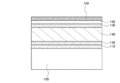
図1は、本発明の一態様における光電変換装置の断面図であり、基板100上に第1の電極110、第1のシリコン半導体層130、第2のシリコン半導体層140、第3のシリコン半導体層150、透光性導電膜160、第2の電極120が順に積層されている。なお、図1の構成の光電変換装置は、基板100側が受光面となるが、基板100上に形成する積層の順序を上記とは逆にして、基板100とは逆側を受光面としても良い。
FIG. 1 is a cross-sectional view of a photoelectric conversion device according to one embodiment of the present invention, in which a
基板100には、例えば、青板ガラス、白板ガラス、鉛ガラス、または結晶化ガラスなどのガラス基板を用いることができる。また、アルミノシリケートガラス、バリウムホウケイ酸ガラス、またはアルミノホウケイ酸ガラスなどの無アルカリガラス基板や石英基板を用いることができる。本実施の形態では、基板100にガラス基板を用いる。
As the
また、基板100には、樹脂基板を用いることもできる。例えば、ポリエーテルスルホン(PES)、ポリエチレンテレフタレート(PET)、ポリエチレンナフタレート(PEN)、ポリカーボネート(PC)、ポリアミド系合成繊維、ポリエーテルエーテルケトン(PEEK)、ポリスルホン(PSF)、ポリエーテルイミド(PEI)、ポリアリレート(PAR)、ポリブチレンテレフタレート(PBT)、ポリイミド、アクリロニトリルブタジエンスチレン樹脂、ポリ塩化ビニル、ポリプロピレン、ポリ酢酸ビニル、アクリル樹脂などが挙げられる。
The
第1の電極110には、例えば、インジウム錫酸化物、珪素を含むインジウム錫酸化物、亜鉛を含む酸化インジウム、酸化亜鉛、ガリウムを含む酸化亜鉛、アルミニウムを含む酸化亜鉛、酸化錫、フッ素を含む酸化錫、またはアンチモンを含む酸化錫等の透光性導電膜を用いることができる。上記透光性導電膜は単層に限らず、異なる膜の積層でも良い。例えば、インジウム錫酸化物とアルミニウムを含む酸化亜鉛の積層や、インジウム錫酸化物とフッ素を含む酸化錫の積層などを用いることができる。膜厚は総厚で10nm以上1000nm以下とする。
The
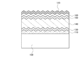
また、図2に示すように、第1の電極110の表面に凹凸を設けた構成としても良い。第1の電極110の表面に凹凸を設けることで、その上に積層する各層の界面にも凹凸が形成することができる。該凹凸により、基板表面での多重反射、光電変換層内での光路長の増大、及び裏面電極による反射光の表面での全反射効果(光閉じ込め効果)が付与され、光電変換装置の電気特性を向上させることができる。
In addition, as illustrated in FIG. 2, a structure in which unevenness is provided on the surface of the
第1のシリコン半導体層130にはp型のシリコン半導体膜を用いる。なお、第1のシリコン半導体層130の膜厚は、1nm以上50nm以下とすることが好ましい。また、第1のシリコン半導体層130には非晶質シリコンを用いることもできるが、より低抵抗の微結晶シリコンまたは多結晶シリコンを用いることが好ましい。
A p-type silicon semiconductor film is used for the first
第2のシリコン半導体層140には、i型のシリコン半導体膜を用いる。なお、本明細書において、i型の半導体とは、フェルミ準位がバンドギャップの中央に位置する所謂真性半導体の他、半導体に含まれるp型若しくはn型を付与する不純物が1×1020cm−3以下の濃度であり、暗伝導度に対して光伝導度が100倍以上である半導体を指す。このi型のシリコン半導体には、周期表第13族または第15族の元素が不純物として含まれるものであっても良い。
An i-type silicon semiconductor film is used for the second
第2のシリコン半導体層140に用いるi型のシリコン半導体膜には、非単結晶シリコン、非晶質シリコン、微結晶シリコン、または多結晶シリコンを用いることが好ましい。非晶質シリコンは、可視光領域に分光感度のピークを有しており、蛍光灯下の様な低照度の環境で高い光電変換能力を示す光電変換装置を形成することができる。また、微結晶シリコン及び多結晶シリコンは、可視光領域よりも長波長側の波長領域に分光感度のピークを有しており、太陽光を光源とする屋外で高い光電変換能力を示す光電変換装置を形成することができる。なお、第2のシリコン半導体層140に非晶質シリコンを用いる場合の膜厚は、100nm以上600nm以下とすることが好ましく、微結晶シリコンまたは多結晶シリコンを用いる場合の膜厚は、1μm以上100μm以下とすることが好ましい。
As the i-type silicon semiconductor film used for the second
第3のシリコン半導体層150にはn型のシリコン半導体膜を用いる。なお、第3のシリコン半導体層150の膜厚は、1nm以上50nm以下とすることが好ましい。また、第3のシリコン半導体層150には非晶質シリコンを用いることもできるが、より低抵抗の微結晶シリコンまたは多結晶シリコンを用いることが好ましい。
An n-type silicon semiconductor film is used for the third
以上説明した、p型の第1のシリコン半導体層130、i型の第2のシリコン半導体層140、n型の第3のシリコン半導体層150の積層によりp−i−n型の接合を形成することができる。
A p-i-n type junction is formed by stacking the p-type first
透光性導電膜160は、無機化合物と有機化合物の複合材料である。該無機化合物としては、遷移金属酸化物を用いることができ、特に元素周期表における第4族乃至第8族に属する金属の酸化物であることが好ましい。具体的には酸化バナジウム、酸化ニオブ、酸化タンタル、酸化クロム、酸化モリブデン、酸化タングステン、酸化マンガン、酸化レニウムなどを用いることができる。中でも特に、酸化モリブデンは大気中でも安定であり、吸湿性が低く、扱いやすいため好ましい。
The light-transmitting
また、上記有機化合物としては、芳香族アミン化合物、カルバゾール誘導体、芳香族炭化水素、高分子化合物(オリゴマー、デンドリマー、ポリマー等)、ジベンゾフラン骨格もしくはジベンゾチオフェン骨格を含む複素環化合物など、種々の化合物を用いることができる。なお、複合材料に用いる有機化合物としては、正孔輸送性の高い有機化合物を用いる。具体的には、10−6cm2/Vs以上の正孔移動度を有する物質であることが好ましい。但し、電子よりも正孔の輸送性の高い物質であれば、これら以外のものを用いてもよい。 Examples of the organic compound include various compounds such as aromatic amine compounds, carbazole derivatives, aromatic hydrocarbons, polymer compounds (oligomers, dendrimers, polymers, etc.), heterocyclic compounds containing a dibenzofuran skeleton or a dibenzothiophene skeleton. Can be used. Note that as the organic compound used for the composite material, an organic compound having a high hole-transport property is used. Specifically, a substance having a hole mobility of 10 −6 cm 2 / Vs or higher is preferable. Note that other than these substances, any substance that has a property of transporting more holes than electrons may be used.
上述の遷移金属酸化物は電子受容性を有し、正孔輸送性の高い有機化合物との複合材料はキャリア密度が高く、導電性を示す。また、該複合材料は、可視光域から赤外域の広い波長範囲に渡って透過率が高い特性を有している。 The above-described transition metal oxide has an electron-accepting property, and a composite material with an organic compound having a high hole-transporting property has high carrier density and conductivity. In addition, the composite material has a characteristic of high transmittance over a wide wavelength range from the visible light region to the infrared region.
また、該複合材料は安定であり、シリコン膜との界面に酸化シリコンを生じさせないことから界面の欠陥を低減させることができ、キャリアのライフタイムを向上させることができる。 In addition, since the composite material is stable and does not generate silicon oxide at the interface with the silicon film, defects at the interface can be reduced and the lifetime of carriers can be improved.
該複合材料をパッシベーション膜としてn型の単結晶シリコン基板上に形成したときのキャリアのライフタイムは、有機化合物に4−フェニル−4’−(9−フェニルフルオレン−9−イル)トリフェニルアミン(略称:BPAFLP)、無機化合物に酸化モリブデン(VI)を用いた場合で、700μsec以上、有機化合物に4,4’−ビス[N−(1−ナフチル)−N−フェニルアミノ]ビフェニル(略称:NPB)、無機化合物に酸化モリブデン(VI)を用いた場合で、400μsec以上であることが実験で確かめられている。なお、パッシベーション膜を形成しないn型の単結晶シリコン基板のライフタイムは、約40μsec、該単結晶シリコン基板の両面にスパッタ法でインジウム錫酸化物(ITO)を成膜した場合のライフタイムは、約30μsecである。 When the composite material is formed as a passivation film on an n-type single crystal silicon substrate, the lifetime of carriers is 4-phenyl-4 ′-(9-phenylfluoren-9-yl) triphenylamine ( Abbreviation: BPAFLP), when molybdenum oxide (VI) is used as the inorganic compound, 700 μsec or more, and 4,4′-bis [N- (1-naphthyl) -N-phenylamino] biphenyl (abbreviation: NPB) as the organic compound ), When molybdenum oxide (VI) is used as the inorganic compound, it has been confirmed by experiments that it is 400 μsec or more. Note that the lifetime of an n-type single crystal silicon substrate that does not form a passivation film is about 40 μsec, and the lifetime when indium tin oxide (ITO) is formed on both surfaces of the single crystal silicon substrate by sputtering is as follows: About 30 μsec.
第2の電極120には、アルミニウム、チタン、ニッケル、銀、モリブデン、タンタル、タングステン、クロム、銅またはステンレス等の金属膜を用いることができる。金属膜は単層に限らず、異なる膜の積層でも良い。例えば、ステンレスとアルミニウムの積層や、銀とアルミニウムの積層などを用いることができる。膜厚は総厚で100nm以上600nm以下、好ましくは100nm以上300nm以下とする。
For the
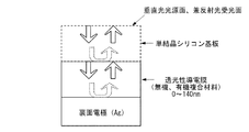
次に、裏面電極(図1の構成では、第2の電極120)近傍における反射率の計算結果を説明する。図5は、計算のモデルであり、裏面電極である銀、透光性導電膜(BPAFLPと酸化モリブデンの複合材料)、及び単結晶シリコン基板を積層したものである。光は裏面電極に対して垂直に照射されるものとし、単結晶シリコン基板の表面を光源面、及び反射光の受光面とする。
Next, the calculation result of the reflectance in the vicinity of the back electrode (
このとき、単結晶シリコン基板の板厚は極薄いものと仮定し、その光吸収は考慮されないものとする。したがって、非晶質シリコン、微結晶シリコンまたは多結晶シリコンのいずれを用いた場合でも計算結果は同等となる。また、透光性導電膜の構成材料に一例としてBPAFLPを用いているが、他の有機材料であっても、屈折率(n)及び消衰係数(k)がBPAFLPと近似していれば、計算結果は同等となる。 At this time, the plate thickness of the single crystal silicon substrate is assumed to be extremely thin, and the light absorption is not considered. Accordingly, the calculation results are the same regardless of whether amorphous silicon, microcrystalline silicon, or polycrystalline silicon is used. Moreover, although BPAFLP is used as an example of the constituent material of the light-transmitting conductive film, even if it is another organic material, if the refractive index (n) and the extinction coefficient (k) are close to BPAFLP, The calculation results are equivalent.
計算には、光学シミュレーションソフトの「DiffractMOD」(RSoft社製)を用い、透光性導電膜の膜厚を0から140nmまで10nm毎に変化させたときの波長範囲500nmから1200nmの反射率を算出した。なお、500nmより短波長側の波長の光は、シリコン薄膜の吸収が大きく、裏面への到達は無視できるものとして計算から除外している。表1には、本計算に用いた各材料の屈折率(n)及び消衰係数(k)の代表的な波長における数値である。なお、実際の計算は、20nm毎に波長を変化させて行っている。 For the calculation, “DiffractMOD” (manufactured by RSsoft) of optical simulation software is used, and the reflectance in the wavelength range of 500 nm to 1200 nm is calculated when the thickness of the translucent conductive film is changed every 10 nm from 0 to 140 nm. did. Note that light having a wavelength shorter than 500 nm is excluded from the calculation because the silicon thin film has a large absorption and can reach the back surface. Table 1 shows numerical values at typical wavelengths of the refractive index (n) and extinction coefficient (k) of each material used in this calculation. The actual calculation is performed by changing the wavelength every 20 nm.

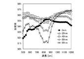
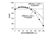
図6は、上記条件における反射率の計算結果である。なお、図を明確にするために、透光性導電膜の膜厚を0nm、20nm、40nm、60nm、80nmの計算結果のみ図示している。図7には、計算結果から算出した透光性導電膜の膜厚毎の平均の反射率を示す。図中の白丸は、波長500nmから1200nmまでの反射率を平均した結果であり、黒丸は、波長500nmから800nmまでの反射率を平均した結果である。光吸収層(図1の構成では、第2のシリコン半導体層140)の材質によって分光感度が異なるため、光吸収層に微結晶シリコンまたは多結晶シリコンを用いる場合は、波長500nmから1200nmまでの平均の反射率、光吸収層に非晶質シリコンを用いる場合は、波長500nmから800nmまでの平均の反射率を考慮すると良い。
FIG. 6 is a calculation result of the reflectance under the above conditions. For the sake of clarity, only the calculation results of the transparent conductive film having a thickness of 0 nm, 20 nm, 40 nm, 60 nm, and 80 nm are shown. In FIG. 7, the average reflectance for every film thickness of the translucent conductive film computed from the calculation result is shown. The white circles in the figure are the results of averaging the reflectance from a wavelength of 500 nm to 1200 nm, and the black circles are the result of averaging the reflectance from a wavelength of 500 nm to 800 nm. Since the spectral sensitivity differs depending on the material of the light absorption layer (second
この結果より、裏面側での反射率を向上させる透光性導電膜の膜厚の適切な範囲は、0nmより厚く、80nmより薄い範囲であるといえ、好ましくは、20nm以上60nm以下、更に好ましくは20nm以上50nm以下である。 From this result, it can be said that the appropriate range of the film thickness of the translucent conductive film for improving the reflectance on the back surface side is a range of thicker than 0 nm and thinner than 80 nm, preferably 20 nm or more and 60 nm or less, more preferably Is 20 nm or more and 50 nm or less.
なお、本発明の一態様における光電変換装置は、図3に示すように、基板200上に、第1の電極210、第1のシリコン半導体層230、第2のシリコン半導体層240、第3のシリコン半導体層250、第1の透光性導電膜310、第4のシリコン半導体層260、第5のシリコン半導体層270、第6のシリコン半導体層280、第2の透光性導電膜320、及び第2の電極220を設けた構成としても良い。該構成の光電変換装置は、第2のシリコン半導体層240を光吸収層とするトップセルと、第5のシリコン半導体層270を光吸収層とするボトムセルを直列に接続した、所謂タンデム型の光電変換装置である。
Note that in the photoelectric conversion device of one embodiment of the present invention, as illustrated in FIG. 3, the
図3の光電変換装置では、第2のシリコン半導体層240に非晶質シリコンを用い、第5のシリコン半導体層270に微結晶シリコンまたは多結晶シリコンを用いる。第1のシリコン半導体層230及び第4のシリコン半導体層260には、前述した第1のシリコン半導体層130と同じ材料を用いることができ、第3のシリコン半導体層250及び第6のシリコン半導体層280には、前述した第3のシリコン半導体層150と同じ材料を用いることができる。第1の電極210及び第1の透光性導電膜310には、前述した第1の電極110と同じ材料を用いることができ、第2の透光性導電膜には、前述した透光性導電膜160と同じ材料を用いることができる。また、第2の電極220には、前述した第2の電極120と同じ材料を用いることができる。
In the photoelectric conversion device in FIG. 3, amorphous silicon is used for the second
基板100側から第1の電極210を透過してトップセルに侵入した光のうち、主に可視光よりも短波長側の光は、第2のシリコン半導体層240において光電変換され、トップセルを透過する主に可視光よりも長波長側の光は、第5のシリコン半導体層270で光電変換される。したがって、広い波長範囲の光を有効に利用することができ、光電変換装置の変換効率を向上させることができる。
Of the light that has passed through the
次に、本発明の一態様における光電変換装置の作製方法について図4を用いて説明する。以下に示す光電変換装置の作製方法は、図1の光電変換装置を直列に複数接続した集積型光電変換装置の作製方法であり、完成した構造は、図4(D)に示されている。 Next, a method for manufacturing a photoelectric conversion device according to one embodiment of the present invention is described with reference to FIGS. The photoelectric conversion device manufacturing method described below is a manufacturing method of an integrated photoelectric conversion device in which a plurality of photoelectric conversion devices in FIG. 1 are connected in series, and a completed structure is illustrated in FIG.
まず、基板100上に第1の電極110となる透光性導電膜を形成する。ここでは、スパッタ法を用い、膜厚100nmのインジウム錫酸化物(ITO)を形成する。なお、図2に示すような透光性導電膜の凹凸は、例えば酸化亜鉛系の透光性導電膜を塩酸などの強酸でエッチングすることで容易に形成することができる。
First, a light-transmitting conductive film to be the
本実施の形態では基板100にガラス基板を用いるが、例えば100μm前後の樹脂基板を用いれば、Roll−to−Rollプロセスを行うことができる。
In this embodiment, a glass substrate is used as the
Roll−to−Rollプロセスには、スパッタ法やプラズマCVD法などの成膜工程だけでなく、スクリーン印刷法やレーザ加工法などの工程も含まれる。したがって、光電変換装置のほぼ全ての製造工程をRoll−to−Rollプロセスで行うこともできる。また、途中までの工程をRoll−to−Rollプロセスで行い、シート状に分断して、その後の工程をシート単位で行っても良い。例えば、分断したシートをセラミックや金属、またはそれらの複合体等で形成された枠に貼付けることで、ガラス基板等と同様に取り扱うことができる。 The Roll-to-Roll process includes not only film forming processes such as sputtering and plasma CVD, but also processes such as screen printing and laser processing. Therefore, almost all manufacturing steps of the photoelectric conversion device can be performed by a Roll-to-Roll process. Further, the process up to the middle may be performed by a Roll-to-Roll process, divided into sheets, and the subsequent processes may be performed on a sheet basis. For example, the cut sheet can be handled in the same manner as a glass substrate or the like by sticking it to a frame formed of ceramic, metal, or a composite thereof.
次に、該透光性導電膜を複数に分離する第1の分離溝410を形成する(図4(A)参照)。該分離溝は、レーザ加工等で形成することができる。このレーザ加工に用いられるレーザは、可視光領域または赤外光領域の連続発振またはパルス発振レーザを用いることが好ましい。例えば、Nd−YAGレーザの基本波(波長1064nm)や第二高調波(波長532nm)を用いることができる。なお、ここで該分離溝の一部が基板100に達しても良い。また、この段階で透光性導電膜が分離加工されることにより第1の電極110が形成される。
Next, a
次に、プラズマCVD法を用いて、第1のシリコン半導体層130として膜厚30nmのp型の微結晶シリコンを成膜する。本実施の形態では、プラズマCVD法を用い、p型を付与する不純物を含むドーピングガスを原料ガスに混合してp型の微結晶シリコンを形成する。p型を付与する不純物としては、代表的には周期表第13族元素であるホウ素やアルミニウムなどが挙げられる。例えば、ジボランなどのドーピングガスをシラン等の原料ガスに混合することで、p型の微結晶シリコンを形成することができる。なお、第1のシリコン半導体層130は、非晶質シリコンで形成しても良いが、より低抵抗な微結晶シリコンで形成することが好ましい。
Next, a p-type microcrystalline silicon film with a thickness of 30 nm is formed as the first
次に、第2のシリコン半導体層140として膜厚600nmのi型の非晶質シリコンを成膜する。原料ガスには、シランまたはジシランを用いることができ、水素を添加しても良い。このとき、膜中に含まれる大気成分がドナーとなる場合があるため、導電型がよりi型に近づくように、原料ガス中にホウ素(B)を添加しても良い。この場合、i型の非晶質シリコン中のホウ素濃度が0.001at.%以上0.1at.%以下となる様にする。
Next, i-type amorphous silicon having a thickness of 600 nm is formed as the second
次に、第3のシリコン半導体層150として、膜厚30nmのn型の微結晶シリコンを成膜する(図4(B)参照)。本実施の形態では、プラズマCVD法を用い、n型を付与する不純物を含むドーピングガスを原料ガスに混合してn型の微結晶シリコンを形成する。n型を付与する不純物としては、代表的には周期表第15族元素であるリン、ヒ素、またはアンチモンなどが挙げられる。例えば、ホスフィンなどのドーピングガスをシラン等の原料ガスに混合することで、n型の微結晶シリコンを形成することができる。なお、第3のシリコン半導体層150は、非晶質シリコンで形成しても良いが、より低抵抗な微結晶シリコンで形成することが好ましい。
Next, n-type microcrystalline silicon with a thickness of 30 nm is formed as the third silicon semiconductor layer 150 (see FIG. 4B). In this embodiment mode, a plasma CVD method is used, and a doping gas containing an impurity imparting n-type is mixed with a source gas to form n-type microcrystalline silicon. Typical examples of the impurity imparting n-type include phosphorus, arsenic, antimony, and the like, which are Group 15 elements of the periodic table. For example, n-type microcrystalline silicon can be formed by mixing a doping gas such as phosphine with a source gas such as silane. Note that the third
次に、第1のシリコン半導体層130、第2のシリコン半導体層140及び第3のシリコン半導体層150の積層を複数に分離する第2の分離溝420を形成する(図4(C)参照)。該分離溝は、レーザ加工等で形成することができる。このレーザ加工に用いられるレーザは、可視光領域の連続発振またはパルス発振レーザを用いることが好ましい。例えば、Nd−YAGレーザの第二高調波(波長532nm)などを用いることができる。
Next, a
次に、第2の分離溝420、及び第3のシリコン半導体層150を覆う様に透光性導電膜160を形成する。透光性導電膜160は、前述した無機化合物及び有機化合物の共蒸着法により形成する。共蒸着法とは、一つの処理室内で複数の蒸発源から同時に蒸着を行う蒸着法である。成膜は高真空下で行われることが好ましい。高真空は、成膜室内を真空排気手段により真空度が5×10⁻³Pa以下、好ましくは10−4Pa乃至10−6Pa程度の範囲なるように真空排気することで得られる。
Next, a light-transmitting
本実施の形態では、透光性導電膜160は、4−フェニル−4’−(9−フェニルフルオレン−9−イル)トリフェニルアミン(略称:BPAFLP)及び酸化モリブデン(VI)を共蒸着することにより形成した。その膜厚は、50nmとし、BPAFLPと酸化モリブデンの比率は、重量比で2:1(=BPAFLP:酸化モリブデン)となるように調節した。
In this embodiment, the light-transmitting
次に、透光性導電膜160上に導電膜を形成する。ここでは、スパッタ法を用い、膜厚5nmの銀と膜厚300nmのアルミニウムを順に積層する。
Next, a conductive film is formed over the light-transmitting
そして、該導電膜を複数に分離する第3の分離溝430を形成する(図4(D)参照)。該分離溝は、レーザ加工等で形成することができる。このレーザ加工に用いられるレーザは、赤外光領域の連続発振またはパルス発振レーザを用いることが好ましい。例えば、Nd−YAGレーザの基本波(波長1064nm)などを用いることができる。また、この段階で導電膜が分離加工されることにより第2の電極120、第1の端子510及び第2の端子520が形成される。ここで、第1の端子510及び第2の端子520は取り出し電極となる。
Then, a
以上により、本発明の一態様の光電変換装置を作製することができる。なお、本実施の形態では、図1に例示した光電変換装置を集積化した構成の作製方法を説明したが、図2、及び図3の構成の光電変換装置を同様の方法で集積化することもできる。 Through the above steps, the photoelectric conversion device of one embodiment of the present invention can be manufactured. Note that in this embodiment, the method for manufacturing the structure in which the photoelectric conversion devices illustrated in FIG. 1 are integrated is described; however, the photoelectric conversion devices having the structures in FIGS. 2 and 3 are integrated by a similar method. You can also.
本実施の形態は、他の実施の形態に記載した構成と適宜組み合わせて実施することが可能である。 This embodiment can be implemented in appropriate combination with the structures described in the other embodiments.
(実施の形態2)
本実施の形態では、実施の形態1で示した透光性導電膜について説明する。
(Embodiment 2)
In this embodiment, the light-transmitting conductive film described in Embodiment 1 is described.
実施の形態1で示した光電変換装置の反射層として用いられる透光性導電膜には、遷移金属酸化物と有機化合物とを複合した材料を用いることができる。なお、本明細書中において、複合とは、単に2つの材料を混合させるだけでなく、複数の材料を混合することによって材料間での電荷の授受が行われ得る状態になることを言う。 For the light-transmitting conductive film used as the reflective layer of the photoelectric conversion device described in Embodiment 1, a material in which a transition metal oxide and an organic compound are combined can be used. Note that in this specification, the term “composite” means that not only two materials are mixed but also a state in which charges can be transferred between the materials by mixing a plurality of materials.
上記遷移金属酸化物としては、電子受容性を有する遷移金属酸化物を用いることができる。具体的には、遷移金属酸化物の中でも、元素周期表における第4族乃至第8族に属する金属の酸化物であることが好ましい。特に、酸化バナジウム、酸化ニオブ、酸化タンタル、酸化クロム、酸化モリブデン、酸化タングステン、酸化マンガン、酸化レニウムは電子受容性が高いため好ましい。中でも特に、酸化モリブデンは大気中でも安定であり、吸湿性が低く、扱いやすいため好ましい。 As the transition metal oxide, a transition metal oxide having an electron accepting property can be used. Specifically, among transition metal oxides, an oxide of a metal belonging to Groups 4 to 8 in the periodic table is preferable. In particular, vanadium oxide, niobium oxide, tantalum oxide, chromium oxide, molybdenum oxide, tungsten oxide, manganese oxide, and rhenium oxide are preferable because of their high electron-accepting properties. Among these, molybdenum oxide is especially preferable because it is stable in the air, has a low hygroscopic property, and is easy to handle.
また、上記有機化合物としては、芳香族アミン化合物、カルバゾール誘導体、芳香族炭化水素、高分子化合物(オリゴマー、デンドリマー、ポリマー等)、ジベンゾフラン骨格もしくはジベンゾチオフェン骨格を含む複素環化合物など、種々の化合物を用いることができる。なお、複合材料に用いる有機化合物としては、正孔輸送性の高い有機化合物を用いる。具体的には、10−6cm2/Vs以上の正孔移動度を有する物質であることが好ましい。但し、電子よりも正孔の輸送性の高い物質であれば、これら以外のものを用いてもよい。 Examples of the organic compound include various compounds such as aromatic amine compounds, carbazole derivatives, aromatic hydrocarbons, polymer compounds (oligomers, dendrimers, polymers, etc.), heterocyclic compounds containing a dibenzofuran skeleton or a dibenzothiophene skeleton. Can be used. Note that as the organic compound used for the composite material, an organic compound having a high hole-transport property is used. Specifically, a substance having a hole mobility of 10 −6 cm 2 / Vs or higher is preferable. Note that other than these substances, any substance that has a property of transporting more holes than electrons may be used.
上記遷移金属酸化物と上記有機化合物とを含む複合材料では、有機化合物の最高被占有軌道準位(HOMO準位)にある電子が、遷移金属酸化物の伝導帯に移動することにより、遷移金属酸化物と有機化合物との間に相互作用が生じる。この相互作用により、遷移金属酸化物と有機化合物とを含む複合材料は、キャリア密度が高く、導電性を示す。 In the composite material including the transition metal oxide and the organic compound, electrons in the highest occupied orbital level (HOMO level) of the organic compound move to the conduction band of the transition metal oxide, whereby the transition metal Interaction occurs between the oxide and the organic compound. By this interaction, the composite material including the transition metal oxide and the organic compound has high carrier density and conductivity.
以下では、複合材料に用いることのできる有機化合物を具体的に列挙する。 Below, the organic compound which can be used for a composite material is listed concretely.
例えば、複合材料に用いることのできる芳香族アミン化合物としては、例えば、4,4’−ビス[N−(1−ナフチル)−N−フェニルアミノ]ビフェニル(略称:NPB)、N,N’−ビス(3−メチルフェニル)−N,N’−ジフェニル−[1,1’−ビフェニル]−4,4’−ジアミン(略称:TPD)、4,4’,4’’−トリス(N,N−ジフェニルアミノ)トリフェニルアミン(略称:TDATA)、4,4’,4’’−トリス[N−(3−メチルフェニル)−N−フェニルアミノ]トリフェニルアミン(略称:MTDATA)、N,N’−ビス(スピロ−9,9’−ビフルオレン−2−イル)−N,N’−ジフェニルベンジジン(略称:BSPB)等を用いることができる。また、N,N’−ビス(4−メチルフェニル)−N,N’−ジフェニル−p−フェニレンジアミン(略称:DTDPPA)、4,4’−ビス[N−(4−ジフェニルアミノフェニル)−N−フェニルアミノ]ビフェニル(略称:DPAB)、N,N’−ビス[4−[ビス(3−メチルフェニル)アミノ]フェニル]−N,N’−ジフェニル−[1,1’−ビフェニル]−4,4’−ジアミン(略称:DNTPD)、1,3,5−トリス[N−(4−ジフェニルアミノフェニル)−N−フェニルアミノ]ベンゼン(略称:DPA3B)、4−フェニル−4’−(9−フェニルフルオレン−9−イル)トリフェニルアミン(略称:BPAFLP)、4,4’−ビス[N−(9,9−ジメチルフルオレン−2−イル)−N−フェニルアミノ]ビフェニル(略称:DFLDPBi)、4,4’−ビス[N−(スピロ−9,9’−ビフルオレン−2−イル)−N―フェニルアミノ]ビフェニル(略称:BSPB)等を挙げることができる。 For example, as an aromatic amine compound that can be used for the composite material, for example, 4,4′-bis [N- (1-naphthyl) -N-phenylamino] biphenyl (abbreviation: NPB), N, N′— Bis (3-methylphenyl) -N, N′-diphenyl- [1,1′-biphenyl] -4,4′-diamine (abbreviation: TPD), 4,4 ′, 4 ″ -tris (N, N -Diphenylamino) triphenylamine (abbreviation: TDATA), 4,4 ', 4 "-tris [N- (3-methylphenyl) -N-phenylamino] triphenylamine (abbreviation: MTDATA), N, N '-Bis (spiro-9,9'-bifluoren-2-yl) -N, N'-diphenylbenzidine (abbreviation: BSPB) or the like can be used. N, N′-bis (4-methylphenyl) -N, N′-diphenyl-p-phenylenediamine (abbreviation: DTDPPA), 4,4′-bis [N- (4-diphenylaminophenyl) -N -Phenylamino] biphenyl (abbreviation: DPAB), N, N'-bis [4- [bis (3-methylphenyl) amino] phenyl] -N, N'-diphenyl- [1,1'-biphenyl] -4 , 4′-diamine (abbreviation: DNTPD), 1,3,5-tris [N- (4-diphenylaminophenyl) -N-phenylamino] benzene (abbreviation: DPA3B), 4-phenyl-4 ′-(9 -Phenylfluoren-9-yl) triphenylamine (abbreviation: BPAFLP), 4,4'-bis [N- (9,9-dimethylfluoren-2-yl) -N-phenylamino] biphe Le (abbreviation: DFLDPBi), 4,4'-bis [N- (spiro-9,9'-bifluoren-2-yl) -N- phenylamino] biphenyl (abbreviation: BSPB), and the like.
複合材料に用いることのできるカルバゾール誘導体としては、具体的には、3−[N−(9−フェニルカルバゾール−3−イル)−N−フェニルアミノ]−9−フェニルカルバゾール(略称:PCzPCA1)、3,6−ビス[N−(9−フェニルカルバゾール−3−イル)−N−フェニルアミノ]−9−フェニルカルバゾール(略称:PCzPCA2)、3−[N−(1−ナフチル)−N−(9−フェニルカルバゾール−3−イル)アミノ]−9−フェニルカルバゾール(略称:PCzPCN1)等を挙げることができる。 Specific examples of the carbazole derivative that can be used for the composite material include 3- [N- (9-phenylcarbazol-3-yl) -N-phenylamino] -9-phenylcarbazole (abbreviation: PCzPCA1), 3 , 6-Bis [N- (9-phenylcarbazol-3-yl) -N-phenylamino] -9-phenylcarbazole (abbreviation: PCzPCA2), 3- [N- (1-naphthyl) -N- (9- Phenylcarbazol-3-yl) amino] -9-phenylcarbazole (abbreviation: PCzPCN1) and the like.
複合材料に用いることのできるカルバゾール誘導体としては、4,4’−ジ(N−カルバゾリル)ビフェニル(略称:CBP)、1,3,5−トリス[4−(N−カルバゾリル)フェニル]ベンゼン(略称:TCPB)、9−[4−(N−カルバゾリル)フェニル]−10−フェニルアントラセン(略称:CzPA)、1,4−ビス[4−(N−カルバゾリル)フェニル]−2,3,5,6−テトラフェニルベンゼン等を用いることができる。 As the carbazole derivative which can be used for the composite material, 4,4′-di (N-carbazolyl) biphenyl (abbreviation: CBP), 1,3,5-tris [4- (N-carbazolyl) phenyl] benzene (abbreviation) : TCPB), 9- [4- (N-carbazolyl) phenyl] -10-phenylanthracene (abbreviation: CzPA), 1,4-bis [4- (N-carbazolyl) phenyl] -2,3,5,6 -Tetraphenylbenzene or the like can be used.
複合材料に用いることのできる芳香族炭化水素としては、例えば、2−tert−ブチル−9,10−ジ(2−ナフチル)アントラセン(略称:t−BuDNA)、2−tert−ブチル−9,10−ジ(1−ナフチル)アントラセン、9,10−ビス(3,5−ジフェニルフェニル)アントラセン(略称:DPPA)、2−tert−ブチル−9,10−ビス(4−フェニルフェニル)アントラセン(略称:t−BuDBA)、9,10−ジ(2−ナフチル)アントラセン(略称:DNA)、9,10−ジフェニルアントラセン(略称:DPAnth)、2−tert−ブチルアントラセン(略称:t−BuAnth)、9,10−ビス(4−メチル−1−ナフチル)アントラセン(略称:DMNA)、9,10−ビス[2−(1−ナフチル)フェニル]−2−tert−ブチルアントラセン、9,10−ビス[2−(1−ナフチル)フェニル]アントラセン、2,3,6,7−テトラメチル−9,10−ジ(1−ナフチル)アントラセン、2,3,6,7−テトラメチル−9,10−ジ(2−ナフチル)アントラセン、9,9’−ビアントリル、10,10’−ジフェニル−9,9’−ビアントリル、10,10’−ビス(2−フェニルフェニル)−9,9’−ビアントリル、10,10’−ビス[(2,3,4,5,6−ペンタフェニル)フェニル]−9,9’−ビアントリル、アントラセン、テトラセン、ルブレン、ペリレン、2,5,8,11−テトラ(tert−ブチル)ペリレン等が挙げられる。また、この他、ペンタセン、コロネン等も用いることができる。このように、1×10−6cm2/Vs以上の正孔移動度を有し、炭素数14〜42である芳香族炭化水素を用いることがより好ましい。 Examples of aromatic hydrocarbons that can be used for the composite material include 2-tert-butyl-9,10-di (2-naphthyl) anthracene (abbreviation: t-BuDNA), 2-tert-butyl-9,10. -Di (1-naphthyl) anthracene, 9,10-bis (3,5-diphenylphenyl) anthracene (abbreviation: DPPA), 2-tert-butyl-9,10-bis (4-phenylphenyl) anthracene (abbreviation: t-BuDBA), 9,10-di (2-naphthyl) anthracene (abbreviation: DNA), 9,10-diphenylanthracene (abbreviation: DPAnth), 2-tert-butylanthracene (abbreviation: t-BuAnth), 9, 10-bis (4-methyl-1-naphthyl) anthracene (abbreviation: DMNA), 9,10-bis [2- (1-naphthy ) Phenyl] -2-tert-butylanthracene, 9,10-bis [2- (1-naphthyl) phenyl] anthracene, 2,3,6,7-tetramethyl-9,10-di (1-naphthyl) anthracene 2,3,6,7-tetramethyl-9,10-di (2-naphthyl) anthracene, 9,9′-bianthryl, 10,10′-diphenyl-9,9′-bianthryl, 10,10′- Bis (2-phenylphenyl) -9,9′-bianthryl, 10,10′-bis [(2,3,4,5,6-pentaphenyl) phenyl] -9,9′-bianthryl, anthracene, tetracene, Examples include rubrene, perylene, 2,5,8,11-tetra (tert-butyl) perylene, and the like. In addition, pentacene, coronene, and the like can also be used. Thus, it is more preferable to use an aromatic hydrocarbon having a hole mobility of 1 × 10 −6 cm 2 / Vs or more and having 14 to 42 carbon atoms.
複合材料に用いることのできる芳香族炭化水素は、ビニル骨格を有していてもよい。ビニル基を有している芳香族炭化水素としては、例えば、4,4’−ビス(2,2−ジフェニルビニル)ビフェニル(略称:DPVBi)、9,10−ビス[4−(2,2−ジフェニルビニル)フェニル]アントラセン(略称:DPVPA)等が挙げられる。 The aromatic hydrocarbon that can be used for the composite material may have a vinyl skeleton. As the aromatic hydrocarbon having a vinyl group, for example, 4,4′-bis (2,2-diphenylvinyl) biphenyl (abbreviation: DPVBi), 9,10-bis [4- (2,2- Diphenylvinyl) phenyl] anthracene (abbreviation: DPVPA) and the like.
また、複合材料に用いることのできる有機化合物は、ジベンゾフラン骨格もしくはジベンゾチオフェン骨格を含む複素環化合物であっても良い。 The organic compound that can be used for the composite material may be a heterocyclic compound including a dibenzofuran skeleton or a dibenzothiophene skeleton.
また、複合材料に用いることのできる有機化合物は、高分子化合物であってもよく、例えば、ポリ(N−ビニルカルバゾール)(略称:PVK)、ポリ(4−ビニルトリフェニルアミン)(略称:PVTPA)、ポリ[N−(4−{N’−[4−(4−ジフェニルアミノ)フェニル]フェニル−N’−フェニルアミノ}フェニル)メタクリルアミド](略称:PTPDMA)、ポリ[N,N’−ビス(4−ブチルフェニル)−N,N’−ビス(フェニル)ベンジジン](略称:Poly−TPD)などを用いても良い。 The organic compound that can be used for the composite material may be a high molecular compound, such as poly (N-vinylcarbazole) (abbreviation: PVK), poly (4-vinyltriphenylamine) (abbreviation: PVTPA). ), Poly [N- (4- {N ′-[4- (4-diphenylamino) phenyl] phenyl-N′-phenylamino} phenyl) methacrylamide] (abbreviation: PTPDMA), poly [N, N′- Bis (4-butylphenyl) -N, N′-bis (phenyl) benzidine] (abbreviation: Poly-TPD) or the like may be used.
図8は、4−フェニル−4’−(9−フェニルフルオレン−9−イル)トリフェニルアミン(略称:BPAFLP)及び酸化モリブデン(VI)を共蒸着することにより得られる透光性導電膜(膜厚57nm)の分光透過率、並びに一般的な非晶質シリコン光電変換装置の分光感度特性を示したものである。図8に示すように、本実施の形態で示す透光性導電膜は、結晶性シリコンが光吸収を示す波長範囲において透光性に優れているため、裏面電極で反射され、結晶性シリコン内に戻された光は効率良く光電変換に利用される。 FIG. 8 shows a translucent conductive film (film) obtained by co-evaporation of 4-phenyl-4 ′-(9-phenylfluoren-9-yl) triphenylamine (abbreviation: BPAFLP) and molybdenum oxide (VI). The spectral transmittance of 57 nm thick) and the spectral sensitivity characteristics of a typical amorphous silicon photoelectric conversion device are shown. As shown in FIG. 8, the light-transmitting conductive film shown in this embodiment has excellent light-transmitting properties in a wavelength range where crystalline silicon absorbs light. The light returned to is efficiently used for photoelectric conversion.
上述の透光性導電膜の形成方法としては、乾式法、湿式法を問わず、種々の方法を用いることができる。乾式法としては、例えば、複数の蒸着源から複数の蒸着材料を気化させて成膜する共蒸着法などが挙げられる。また、湿式法としては、ゾル−ゲル法などを用いて複合材料を含む組成物を調整し、インクジェット法またはスピンコート法などを用いて成膜することができる。 Various methods can be used as a method for forming the above light-transmitting conductive film regardless of a dry method or a wet method. Examples of the dry method include a co-evaporation method in which a plurality of evaporation materials are vaporized from a plurality of evaporation sources to form a film. As a wet method, a composition containing a composite material can be adjusted using a sol-gel method or the like, and a film can be formed using an inkjet method, a spin coating method, or the like.
以上説明した透光性導電膜を光電変換装置の反射層として用いれば、裏面電極側の反射率が向上し、光電変換装置の電気特性を向上させることができる。 If the translucent conductive film described above is used as a reflective layer of a photoelectric conversion device, the reflectance on the back electrode side can be improved, and the electrical characteristics of the photoelectric conversion device can be improved.
本実施の形態は、他の実施の形態と自由に組み合わすことができる。 This embodiment can be freely combined with any of the other embodiments.
100 基板
110 第1の電極
120 第2の電極
130 第1のシリコン半導体層
140 第2のシリコン半導体層
150 第3のシリコン半導体層
160 透光性導電膜
200 基板
210 第1の電極
220 第2の電極
230 第1のシリコン半導体層
240 第2のシリコン半導体層
250 第3のシリコン半導体層
260 第4のシリコン半導体層
270 第5のシリコン半導体層
280 第6のシリコン半導体層
310 第1の透光性導電膜
320 第2の透光性導電膜
410 第1の分離溝
420 第2の分離溝
430 第3の分離溝
510 第1の端子
520 第2の端子
100
Claims (11)
第1のシリコン半導体層と、
前記第1のシリコン半導体層と接する第2のシリコン半導体層と、
前記第2のシリコン半導体層と接する第3のシリコン半導体層と、
前記第3のシリコン半導体層と接する透光性導電膜と、
を有し、
前記透光性導電膜は、有機化合物及び無機化合物で形成されていることを特徴とする光電変換装置。 Between a pair of electrodes,
A first silicon semiconductor layer;
A second silicon semiconductor layer in contact with the first silicon semiconductor layer;
A third silicon semiconductor layer in contact with the second silicon semiconductor layer;
A translucent conductive film in contact with the third silicon semiconductor layer;
Have
The translucent conductive film is formed of an organic compound and an inorganic compound, and is a photoelectric conversion device.
第1のシリコン半導体層と、
前記第1のシリコン半導体層と接する第2のシリコン半導体層と、
前記第2のシリコン半導体層と接する第3のシリコン半導体層と、
前記第3のシリコン半導体層と接する第1の透光性導電膜と、
前記第1の透光性導電膜と接する第4のシリコン半導体層と、
前記第4のシリコン半導体層と接する第5のシリコン半導体層と、
前記第5のシリコン半導体層と接する第6のシリコン半導体層と、
前記第6のシリコン半導体層と接する第2の透光性導電膜と、
を有し、
前記第2の透光性導電膜は、有機化合物及び無機化合物で形成されていることを特徴とする光電変換装置。 Between a pair of electrodes,
A first silicon semiconductor layer;
A second silicon semiconductor layer in contact with the first silicon semiconductor layer;
A third silicon semiconductor layer in contact with the second silicon semiconductor layer;
A first translucent conductive film in contact with the third silicon semiconductor layer;
A fourth silicon semiconductor layer in contact with the first light-transmitting conductive film;
A fifth silicon semiconductor layer in contact with the fourth silicon semiconductor layer;
A sixth silicon semiconductor layer in contact with the fifth silicon semiconductor layer;
A second translucent conductive film in contact with the sixth silicon semiconductor layer;
Have
The second translucent conductive film is formed of an organic compound and an inorganic compound, and is a photoelectric conversion device.
Priority Applications (1)
| Application Number | Priority Date | Filing Date | Title |
|---|---|---|---|
| JP2012034646A JP2012191189A (en) | 2011-02-21 | 2012-02-21 | Photoelectric conversion device |
Applications Claiming Priority (3)
| Application Number | Priority Date | Filing Date | Title |
|---|---|---|---|
| JP2011034576 | 2011-02-21 | ||
| JP2011034576 | 2011-02-21 | ||
| JP2012034646A JP2012191189A (en) | 2011-02-21 | 2012-02-21 | Photoelectric conversion device |
Publications (2)
| Publication Number | Publication Date |
|---|---|
| JP2012191189A true JP2012191189A (en) | 2012-10-04 |
| JP2012191189A5 JP2012191189A5 (en) | 2015-03-05 |
Family
ID=46651742
Family Applications (1)
| Application Number | Title | Priority Date | Filing Date |
|---|---|---|---|
| JP2012034646A Withdrawn JP2012191189A (en) | 2011-02-21 | 2012-02-21 | Photoelectric conversion device |
Country Status (3)
| Country | Link |
|---|---|
| US (1) | US20120211067A1 (en) |
| JP (1) | JP2012191189A (en) |
| KR (1) | KR20120095786A (en) |
Cited By (2)
| Publication number | Priority date | Publication date | Assignee | Title |
|---|---|---|---|---|
| JP2016111279A (en) * | 2014-12-10 | 2016-06-20 | 国立大学法人東京農工大学 | Multi-junction solar battery and manufacturing method thereof |
| WO2017051749A1 (en) * | 2015-09-25 | 2017-03-30 | 株式会社ブイ・テクノロジー | Radiographic image-capturing device |
Families Citing this family (3)
| Publication number | Priority date | Publication date | Assignee | Title |
|---|---|---|---|---|
| US9437758B2 (en) | 2011-02-21 | 2016-09-06 | Semiconductor Energy Laboratory Co., Ltd. | Photoelectric conversion device |
| JP2013058562A (en) | 2011-09-07 | 2013-03-28 | Semiconductor Energy Lab Co Ltd | Photoelectric conversion device |
| JP6108858B2 (en) | 2012-02-17 | 2017-04-05 | 株式会社半導体エネルギー研究所 | P-type semiconductor material and semiconductor device |
Citations (4)
| Publication number | Priority date | Publication date | Assignee | Title |
|---|---|---|---|---|
| JPH04230081A (en) * | 1990-12-27 | 1992-08-19 | Semiconductor Energy Lab Co Ltd | Photoelectric conversion device |
| JP2010103506A (en) * | 2008-09-26 | 2010-05-06 | Semiconductor Energy Lab Co Ltd | Photoelectric conversion device and method of manufacturing the same |
| WO2010055013A1 (en) * | 2008-11-14 | 2010-05-20 | Epcos Ag | Sensor element and process for assembling a sensor element |
| WO2010113708A1 (en) * | 2009-03-30 | 2010-10-07 | 三菱マテリアル株式会社 | Method of producing solar cell module |
Family Cites Families (7)
| Publication number | Priority date | Publication date | Assignee | Title |
|---|---|---|---|---|
| US4292092A (en) * | 1980-06-02 | 1981-09-29 | Rca Corporation | Laser processing technique for fabricating series-connected and tandem junction series-connected solar cells into a solar battery |
| AU2001276840B2 (en) * | 2000-07-06 | 2006-11-02 | Bp Corporation North America Inc. | Partially transparent photovoltaic modules |
| US7189917B2 (en) * | 2003-03-26 | 2007-03-13 | Canon Kabushiki Kaisha | Stacked photovoltaic device |
| AU2004222793B2 (en) * | 2003-10-27 | 2007-07-26 | Mitsubishi Heavy Industries, Ltd. | Solar cell and process for producing solar cell |
| US7888167B2 (en) * | 2008-04-25 | 2011-02-15 | Semiconductor Energy Laboratory Co., Ltd. | Photoelectric conversion device and method for manufacturing the same |
| US20100269896A1 (en) * | 2008-09-11 | 2010-10-28 | Applied Materials, Inc. | Microcrystalline silicon alloys for thin film and wafer based solar applications |
| WO2010064549A1 (en) * | 2008-12-04 | 2010-06-10 | 三菱電機株式会社 | Method for manufacturing thin-film photoelectric conversion device |
-
2012
- 2012-02-13 KR KR1020120014375A patent/KR20120095786A/en not_active Application Discontinuation
- 2012-02-17 US US13/398,876 patent/US20120211067A1/en not_active Abandoned
- 2012-02-21 JP JP2012034646A patent/JP2012191189A/en not_active Withdrawn
Patent Citations (4)
| Publication number | Priority date | Publication date | Assignee | Title |
|---|---|---|---|---|
| JPH04230081A (en) * | 1990-12-27 | 1992-08-19 | Semiconductor Energy Lab Co Ltd | Photoelectric conversion device |
| JP2010103506A (en) * | 2008-09-26 | 2010-05-06 | Semiconductor Energy Lab Co Ltd | Photoelectric conversion device and method of manufacturing the same |
| WO2010055013A1 (en) * | 2008-11-14 | 2010-05-20 | Epcos Ag | Sensor element and process for assembling a sensor element |
| WO2010113708A1 (en) * | 2009-03-30 | 2010-10-07 | 三菱マテリアル株式会社 | Method of producing solar cell module |
Cited By (2)
| Publication number | Priority date | Publication date | Assignee | Title |
|---|---|---|---|---|
| JP2016111279A (en) * | 2014-12-10 | 2016-06-20 | 国立大学法人東京農工大学 | Multi-junction solar battery and manufacturing method thereof |
| WO2017051749A1 (en) * | 2015-09-25 | 2017-03-30 | 株式会社ブイ・テクノロジー | Radiographic image-capturing device |
Also Published As
| Publication number | Publication date |
|---|---|
| US20120211067A1 (en) | 2012-08-23 |
| KR20120095786A (en) | 2012-08-29 |
Similar Documents
| Publication | Publication Date | Title |
|---|---|---|
| JP6039154B2 (en) | Photoelectric conversion device | |
| JP5897926B2 (en) | Photoelectric conversion device | |
| US9159939B2 (en) | Photoelectric conversion device | |
| KR101558911B1 (en) | Photoelectric conversion device and manufacturing method thereof | |
| KR101292061B1 (en) | Thin film solar cell | |
| JP5894472B2 (en) | Photoelectric conversion device | |
| US8994009B2 (en) | Photoelectric conversion device | |
| JP6254343B2 (en) | Photoelectric conversion device | |
| JP2009152577A (en) | Photoelectric conversion device and manufacturing method thereof | |
| JP2012191189A (en) | Photoelectric conversion device | |
| JP6000566B2 (en) | Photoelectric conversion device | |
| US20100037940A1 (en) | Stacked solar cell | |
| KR101210046B1 (en) | Solar cell and method of fabricating the same | |
| KR20120119807A (en) | Solar cell | |
| KR101529232B1 (en) | Thin-film solar cell and method of fabricating the same | |
| JP2016106437A (en) | Photoelectric conversion device | |
| JP5307280B2 (en) | Thin film photoelectric conversion element | |
| TWI408820B (en) | Solar battery | |
| US20130056052A1 (en) | Thin film solar cell | |
| KR20110011048A (en) | Thin film type solar cell, method and apparatus for manufacturing thereof | |
| KR20130058554A (en) | Solar cell and method of fabricating the same |
Legal Events
| Date | Code | Title | Description |
|---|---|---|---|
| A521 | Request for written amendment filed |
Free format text: JAPANESE INTERMEDIATE CODE: A523 Effective date: 20150114 |
|
| A621 | Written request for application examination |
Free format text: JAPANESE INTERMEDIATE CODE: A621 Effective date: 20150114 |
|
| A977 | Report on retrieval |
Free format text: JAPANESE INTERMEDIATE CODE: A971007 Effective date: 20151028 |
|
| A131 | Notification of reasons for refusal |
Free format text: JAPANESE INTERMEDIATE CODE: A131 Effective date: 20151110 |
|
| A521 | Request for written amendment filed |
Free format text: JAPANESE INTERMEDIATE CODE: A523 Effective date: 20151207 |
|
| A131 | Notification of reasons for refusal |
Free format text: JAPANESE INTERMEDIATE CODE: A131 Effective date: 20160216 |
|
| A521 | Request for written amendment filed |
Free format text: JAPANESE INTERMEDIATE CODE: A523 Effective date: 20160314 |
|
| A02 | Decision of refusal |
Free format text: JAPANESE INTERMEDIATE CODE: A02 Effective date: 20160830 |
|
| A761 | Written withdrawal of application |
Free format text: JAPANESE INTERMEDIATE CODE: A761 Effective date: 20161031 |