JP5999929B2 - Light emitting device package and lighting system using the same - Google Patents
Light emitting device package and lighting system using the same Download PDFInfo
- Publication number
- JP5999929B2 JP5999929B2 JP2012046391A JP2012046391A JP5999929B2 JP 5999929 B2 JP5999929 B2 JP 5999929B2 JP 2012046391 A JP2012046391 A JP 2012046391A JP 2012046391 A JP2012046391 A JP 2012046391A JP 5999929 B2 JP5999929 B2 JP 5999929B2
- Authority
- JP
- Japan
- Prior art keywords
- light
- light emitting
- phosphor
- emitting device
- resin layer
- Prior art date
- Legal status (The legal status is an assumption and is not a legal conclusion. Google has not performed a legal analysis and makes no representation as to the accuracy of the status listed.)
- Active
Links
Images


Classifications
-
- H—ELECTRICITY
- H01—ELECTRIC ELEMENTS
- H01L—SEMICONDUCTOR DEVICES NOT COVERED BY CLASS H10
- H01L33/00—Semiconductor devices with at least one potential-jump barrier or surface barrier specially adapted for light emission; Processes or apparatus specially adapted for the manufacture or treatment thereof or of parts thereof; Details thereof
- H01L33/48—Semiconductor devices with at least one potential-jump barrier or surface barrier specially adapted for light emission; Processes or apparatus specially adapted for the manufacture or treatment thereof or of parts thereof; Details thereof characterised by the semiconductor body packages
- H01L33/50—Wavelength conversion elements
-
- C—CHEMISTRY; METALLURGY
- C09—DYES; PAINTS; POLISHES; NATURAL RESINS; ADHESIVES; COMPOSITIONS NOT OTHERWISE PROVIDED FOR; APPLICATIONS OF MATERIALS NOT OTHERWISE PROVIDED FOR
- C09K—MATERIALS FOR MISCELLANEOUS APPLICATIONS, NOT PROVIDED FOR ELSEWHERE
- C09K11/00—Luminescent, e.g. electroluminescent, chemiluminescent materials
- C09K11/08—Luminescent, e.g. electroluminescent, chemiluminescent materials containing inorganic luminescent materials
- C09K11/0883—Arsenides; Nitrides; Phosphides
-
- C—CHEMISTRY; METALLURGY
- C09—DYES; PAINTS; POLISHES; NATURAL RESINS; ADHESIVES; COMPOSITIONS NOT OTHERWISE PROVIDED FOR; APPLICATIONS OF MATERIALS NOT OTHERWISE PROVIDED FOR
- C09K—MATERIALS FOR MISCELLANEOUS APPLICATIONS, NOT PROVIDED FOR ELSEWHERE
- C09K11/00—Luminescent, e.g. electroluminescent, chemiluminescent materials
- C09K11/08—Luminescent, e.g. electroluminescent, chemiluminescent materials containing inorganic luminescent materials
- C09K11/77—Luminescent, e.g. electroluminescent, chemiluminescent materials containing inorganic luminescent materials containing rare earth metals
- C09K11/7728—Luminescent, e.g. electroluminescent, chemiluminescent materials containing inorganic luminescent materials containing rare earth metals containing europium
- C09K11/7737—Phosphates
- C09K11/7738—Phosphates with alkaline earth metals
- C09K11/7739—Phosphates with alkaline earth metals with halogens
-
- H—ELECTRICITY
- H01—ELECTRIC ELEMENTS
- H01L—SEMICONDUCTOR DEVICES NOT COVERED BY CLASS H10
- H01L33/00—Semiconductor devices with at least one potential-jump barrier or surface barrier specially adapted for light emission; Processes or apparatus specially adapted for the manufacture or treatment thereof or of parts thereof; Details thereof
- H01L33/48—Semiconductor devices with at least one potential-jump barrier or surface barrier specially adapted for light emission; Processes or apparatus specially adapted for the manufacture or treatment thereof or of parts thereof; Details thereof characterised by the semiconductor body packages
- H01L33/52—Encapsulations
-
- H—ELECTRICITY
- H01—ELECTRIC ELEMENTS
- H01L—SEMICONDUCTOR DEVICES NOT COVERED BY CLASS H10
- H01L2224/00—Indexing scheme for arrangements for connecting or disconnecting semiconductor or solid-state bodies and methods related thereto as covered by H01L24/00
- H01L2224/01—Means for bonding being attached to, or being formed on, the surface to be connected, e.g. chip-to-package, die-attach, "first-level" interconnects; Manufacturing methods related thereto
- H01L2224/42—Wire connectors; Manufacturing methods related thereto
- H01L2224/47—Structure, shape, material or disposition of the wire connectors after the connecting process
- H01L2224/48—Structure, shape, material or disposition of the wire connectors after the connecting process of an individual wire connector
- H01L2224/4805—Shape
- H01L2224/4809—Loop shape
- H01L2224/48091—Arched
-
- H—ELECTRICITY
- H01—ELECTRIC ELEMENTS
- H01L—SEMICONDUCTOR DEVICES NOT COVERED BY CLASS H10
- H01L2224/00—Indexing scheme for arrangements for connecting or disconnecting semiconductor or solid-state bodies and methods related thereto as covered by H01L24/00
- H01L2224/01—Means for bonding being attached to, or being formed on, the surface to be connected, e.g. chip-to-package, die-attach, "first-level" interconnects; Manufacturing methods related thereto
- H01L2224/42—Wire connectors; Manufacturing methods related thereto
- H01L2224/47—Structure, shape, material or disposition of the wire connectors after the connecting process
- H01L2224/49—Structure, shape, material or disposition of the wire connectors after the connecting process of a plurality of wire connectors
- H01L2224/491—Disposition
- H01L2224/4911—Disposition the connectors being bonded to at least one common bonding area, e.g. daisy chain
- H01L2224/49113—Disposition the connectors being bonded to at least one common bonding area, e.g. daisy chain the connectors connecting different bonding areas on the semiconductor or solid-state body to a common bonding area outside the body, e.g. converging wires
-
- H—ELECTRICITY
- H01—ELECTRIC ELEMENTS
- H01L—SEMICONDUCTOR DEVICES NOT COVERED BY CLASS H10
- H01L2924/00—Indexing scheme for arrangements or methods for connecting or disconnecting semiconductor or solid-state bodies as covered by H01L24/00
- H01L2924/06—Polymers
- H01L2924/07—Polyamine or polyimide
-
- H—ELECTRICITY
- H01—ELECTRIC ELEMENTS
- H01L—SEMICONDUCTOR DEVICES NOT COVERED BY CLASS H10
- H01L2924/00—Indexing scheme for arrangements or methods for connecting or disconnecting semiconductor or solid-state bodies as covered by H01L24/00
- H01L2924/10—Details of semiconductor or other solid state devices to be connected
- H01L2924/11—Device type
- H01L2924/13—Discrete devices, e.g. 3 terminal devices
- H01L2924/1301—Thyristor
Landscapes
- Engineering & Computer Science (AREA)
- Chemical & Material Sciences (AREA)
- Microelectronics & Electronic Packaging (AREA)
- Inorganic Chemistry (AREA)
- Materials Engineering (AREA)
- Organic Chemistry (AREA)
- Manufacturing & Machinery (AREA)
- Computer Hardware Design (AREA)
- Power Engineering (AREA)
- Led Device Packages (AREA)
Description
本発明の実施例は、発光素子パッケージ及びこれを利用した照明システムに関する。 Embodiments described herein relate generally to a light emitting device package and a lighting system using the same.
発光ダイオード(LED)は、電気エネルギーを光に変換する半導体素子の一種である。発光ダイオードは、蛍光灯、白熱灯など既存の光源に比べて低消費電力、半永久的な寿命、速い応答速度、安全性、環境親和性の長所を有する。これに既存の光源を発光ダイオードに取り替えるための多い研究が進行されているし、発光ダイオードは室内外で使われる各種ランプ、液晶表示装置、電光板、街灯などの照明装置の光源として使用が増加されている成り行きである。 A light emitting diode (LED) is a type of semiconductor element that converts electrical energy into light. The light emitting diode has advantages of low power consumption, semi-permanent lifetime, fast response speed, safety, and environmental friendliness as compared with existing light sources such as fluorescent lamps and incandescent lamps. In addition, much research is underway to replace existing light sources with light-emitting diodes, and light-emitting diodes are increasingly used as light sources for lighting devices such as various lamps, liquid crystal display devices, electric boards, and street lights used indoors and outdoors. It has been done.
発光ダイオードは、順方向電圧印加時にn層電子とp層の正孔が結合して、伝導帯(Conductionband)と価電子帯(Valance band)のエネルギーギャップに該当する程度の光エネルギーを生成することができる。 Light-emitting diodes generate n-layer electrons and p-layer holes when forward voltage is applied, and generate light energy corresponding to the energy gap between the conduction band and valence band. Can do.
発光ダイオードの材質の一種である窒化物半導体は、高い熱的安全性と幅広いバンドギャップエネルギーによって光素子及び高出力電子素子開発分野で大きい関心を受けている。特に、窒化物半導体を利用した青色(Blue)LED、緑(Green)LED、紫外線(UV)LEDなどは常用化されて広く使われている。 Nitride semiconductors, which are a kind of light emitting diode material, have received great interest in the field of optical device and high power electronic device development due to high thermal safety and wide band gap energy. In particular, a blue LED, a green LED, and an ultraviolet (UV) LED using a nitride semiconductor are commonly used and widely used.
本発明の実施例は、新しい構造を有する発光素子パッケージ及びこれを利用したライトユニットを提供する。 Embodiments of the present invention provide a light emitting device package having a new structure and a light unit using the same.
本発明の一実施例は、お互いに異なる青色系列の主ピーク波長を有する発光素子パッケージ及びこれを利用したライトユニットを提供する。 An embodiment of the present invention provides a light emitting device package having a main peak wavelength of a blue series different from each other and a light unit using the same.
本発明の一実施例は、青色蛍光体と青色発光素子を利用して白色カラーを調節することができる発光素子パッケージ及びこれを利用したライトユニットを提供する。 An embodiment of the present invention provides a light emitting device package capable of adjusting a white color using a blue phosphor and a blue light emitting device, and a light unit using the same.
本発明の一実施例による発光素子パッケージは、キャビティを有する胴体と、前記胴体に配置された第1リード電極及び第2リード電極と、前記キャビティ内に配置されて、前記第1リード電極及び第2リード電極のうちの少なくとも1つと電気的に連結されて、410-460nm範囲の第1ピーク波長を発光する発光素子と、前記発光素子上の、第1蛍光体を有する第1樹脂層とを備え、前記第1樹脂層の第1蛍光体は、前記第1主ピーク波長の一部光を励起させて461-480nm範囲の第2主ピーク波長の光を発光して、前記第1主ピーク波長と前記第2主ピーク波長は波長の差を持って等しいカラー帯域の光を含む。 A light emitting device package according to an embodiment of the present invention includes a body having a cavity, a first lead electrode and a second lead electrode disposed in the body, and the first lead electrode and the second lead electrode disposed in the cavity. A light emitting device electrically connected to at least one of the two lead electrodes and emitting a first peak wavelength in the range of 410 to 460 nm; and a first resin layer having a first phosphor on the light emitting device. And the first phosphor of the first resin layer emits light having a second main peak wavelength in the range of 461 to 480 nm by exciting a part of the light having the first main peak wavelength to emit the first main peak. The wavelength and the second main peak wavelength include light of the same color band with a difference in wavelength.
本発明の一実施例による発光素子パッケージは、キャビティを有する胴体と、前記胴体に配置された第1リード電極及び第2リード電極と、前記キャビティ内に配置されて、前記第1リード電極及び第2リード電極のうちの少なくとも1つと電気的に連結されて、410-440nm範囲の第1主ピーク波長を発光する発光素子と、前記発光素子上の、第1蛍光体を含む第1樹脂層と、前記第1樹脂層の上の第2樹脂層とを備え、前記第1樹脂層の第1蛍光体の含量と異なる含量の第2蛍光体を含む第2樹脂層を含んで、前記第1樹脂層の第1蛍光体は、前記第1ピーク波長の一部光を励起させて465-479nm帯域の第2主ピーク波長の光を発光して、前記第1主ピーク波長と前記第2主ピーク波長は、等しいカラー帯域の光を含む。 A light emitting device package according to an embodiment of the present invention includes a body having a cavity, a first lead electrode and a second lead electrode disposed in the body, and the first lead electrode and the second lead electrode disposed in the cavity. A light emitting device electrically connected to at least one of the two lead electrodes and emitting a first main peak wavelength in a range of 410 to 440 nm; a first resin layer including a first phosphor on the light emitting device; And a second resin layer on the first resin layer, the second resin layer including a second phosphor having a content different from the content of the first phosphor in the first resin layer. The first phosphor of the resin layer excites a part of light having the first peak wavelength to emit light having a second main peak wavelength in a 465-479 nm band, and the first main peak wavelength and the second main peak wavelength are emitted. The peak wavelength includes light of equal color band.
本発明の一実施例による発光素子パッケージは、キャビティを有する胴体と、前記キャビティに配置された第1リード電極及び第2リード電極と、前記キャビティ内に配置されて、前記第1リード電極及び第2リード電極のうちの少なくとも1つと電気的に連結されて、第1青色波長を発光する発光素子と、前記発光素子上に配置されて、前記第1青色波長より長波長の第2青色波長を発光する第1蛍光体を含む第1樹脂層とを備え、前記第1樹脂層の第1蛍光体は、461nm-479nm範囲の第2青色波長を発光する。 A light emitting device package according to an embodiment of the present invention includes a body having a cavity, a first lead electrode and a second lead electrode disposed in the cavity, the first lead electrode and the first lead electrode disposed in the cavity. A light emitting device that is electrically connected to at least one of the two lead electrodes and emits a first blue wavelength; and a second blue wavelength that is disposed on the light emitting device and is longer than the first blue wavelength. A first resin layer including a first phosphor that emits light, and the first phosphor of the first resin layer emits a second blue wavelength in a range of 461 nm to 479 nm.
本発明の一実施例による照明システムは、前記の発光素子パッケージのうちの少なくとも1つを備える。 An illumination system according to an embodiment of the present invention includes at least one of the light emitting device packages.
本発明の一実施例は、発光素子パッケージによって発光された光を利用して感性照明効果を改善させてくれることができる。 The embodiment of the present invention can improve the sensitivity lighting effect using light emitted from the light emitting device package.
本発明の一実施例は、発光素子パッケージの光効率を改善させてくれることができる。 The embodiment of the present invention can improve the light efficiency of the light emitting device package.
本発明の一実施例は、色偏差が少ない発光素子パッケージ及びこれを利用したライトユニットを提供することができる。 According to an embodiment of the present invention, a light emitting device package with a small color deviation and a light unit using the same can be provided.
本発明の実施例の説明において、各層(膜)、領域、パターンまたは構造物らが基板、各層(膜)、領域、パッドまたはパターンらの“上(on)”にまたは“下(under)”に形成されることで記載する場合において、“上(on)”と“下(under)”は“直接(directly)”または“他の層を介して(indirectly)”形成されるものをすべて含む。また、各層の上または下に対する基準は、図面を基準で説明する。 In the description of the embodiments of the present invention, each layer (film), region, pattern or structure is “on” or “under” the substrate, each layer (film), region, pad or pattern. Where “on” and “under” include all those formed “directly” or “indirectly”. . Further, the standard for the upper or lower layer will be described with reference to the drawings.
図面で各層の厚さや大きさは、説明の便宜及び明確性のために誇張されるか、または省略されるか、または概略的に図示された。また、各構成要素の大きさは実際大きさを全面的に反映するものではない。 In the drawings, the thickness and size of each layer are exaggerated, omitted, or schematically illustrated for convenience of description and clarity. In addition, the size of each component does not fully reflect the actual size.
以下、添付された図面を参照して本発明の実施例による発光素子に対して説明する。 Hereinafter, a light emitting device according to an embodiment of the present invention will be described with reference to the accompanying drawings.
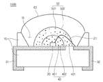
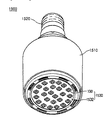
図1は、本発明の一実施例による発光素子パッケージ100の側断面図である。
FIG. 1 is a side sectional view of a light
図1を参照すれば、本発明の一実施例による発光素子パッケージ100は、胴体10、キャビティ15、前記胴体10に配置された第1リード電極31及び第2リード電極32、前記第1リード電極31及び第2リード電極32と電気的に連結されて光を生成する発光素子20、前記発光素子20と前記第2リード電極32を連結するワイヤ21、前記発光素子20を密封するように形成された第1樹脂層40、前記第1樹脂層40上に形成された第2樹脂層50、第2樹脂層50及び前記キャビティ15を満たす第3樹脂層60を備えることができる。
Referring to FIG. 1, a light
前記胴体10は、ポリフタルアミド(PPA:Polyphthalamide)のような樹脂材質、シリコン(Si)、アルミニウム(Al)、アルミニウムナイトライド(AlN)、AlOx、液晶ポリマー(PSG:photo sensitive glass)、ポリアミド9T(PA9T)、シンジオタクチックポリスチレン(SPS)、金属材質、サファイア(Al2O3)、酸化ベリリウム(BeO)、印刷回路基板(PCB:Printed Circuit Board)のうちで少なくとも一つで形成されることができる。前記胴体10は、射出成形、エッチング工程などによって形成されることができるが、これに対して限定しない。
The
前記胴体10が電気伝導性を有する材質で形成された場合、前記胴体10の表面には絶縁膜(図示せず)が形成されて、前記胴体10と前記第1、2リード電極31、32などとの電気的ショートを防止することができる。
When the
また、前記胴体10がシリコン(Si)に形成された場合、前記胴体10には導電型ドーパントを注入する方式でツェナー(zener)ダイオードなどの保護素子を集積回路形態で形成することができる。
When the
前記胴体10には、上部が開放されるように前記キャビティ15が形成されることができる。前記キャビティ15は、例えば、前記胴体10の射出成形過程で形成されるか、またはエッチング工程によって別に形成されることができるし、これに対して限定しない。
The
前記キャビティ15は、コップ形状、または凹な容器形状で形成されることができるし、前記キャビティ15の側面は底面に対して垂直な面や傾いた面になることができる。また、前記キャビティ15を上面から眺めた形状は、円形、四角形、多角形、卵円形などの形状であることがある。前記キャビティ15は、少なくとも一つのリード電極31、32によってコップ構造で形成されることができるし、これに対して限定しない。
The
前記第1リード電極31及び前記第2リード電極32は、お互いに電気的に分離するように前記胴体10に設置されることができる。前記第1、2リード電極31、32は前記発光素子20と電気的に連結されて前記発光素子20に電源を提供することができる。
The
前記第1リード電極31及び前記第2リード電極32の一端は、前記胴体10内に配置されて、他端は前記胴体10に沿って前記胴体10の外側または下面に露出することができる。または、前記第1、2リード電極31、32は、前記胴体10の上面及び下面を貫通して前記発光素子パッケージ100の底面をなすこともでき、前記第1、2リード電極31、32の構造に対して限定しない。
One end of the
前記第1、2リード電極31、32は、メッキ方法、蒸着方法またはフォトリソグラフィ方法などを利用して選択的に形成されることができるし、これに対して限定しない。
The first and second
前記第1、2リード電極31、32は、電気伝導性を有する金属材質、例えば、チタン(Ti)、銅(Cu)、ニッケル(Ni)、金(Au)、クロム(Cr)、タンタル(Ta)、白金(Pt)、スズ(Sn)、銀(Ag)、燐(P)、アルミニウム(Al)、インジウム(In)、パラジウム(Pd)、コバルト(Co)、珪素(Si)、ゲルマニウム(Ge)、ハフニウム(Hf)、ルテニウム(Ru)、または、鉄(Fe)のうちで少なくとも一つの物質を含むことができる。また、前記第1、2リード電極31、32は、単層または多層構造を有するように形成されることができるし、これに対して限定しない。
The first and second
前記発光素子20は、青色発光素子に形成されることができるし、前記第1、2リード電極31、32上に直接接合されて形成されることができる。前記発光素子20が例えば、青色LEDチップの場合、410nm乃至460nm範囲の第1主ピーク波長の値を有することができるし、例えば、420-450nm範囲の第1主ピーク波長を発光するようになる。前記発光素子20は白色カラーを具現するために青色波長と黄色蛍光体から発光された波長を利用して白色カラーバランス(balance)を合わせるようになる。しかし、前記長波長の青色波長は短波長の青色波長に比べてエネルギーが低いから発光効率の向上には限界がある。実施例は、 紫外線(UV:Ultra Violet)範囲の波長に近い青色波長であればあるほど、例えば、450nm以下例えば、420nm±5nmの波長にますます蛍光体がエネルギーをたくさん受けて発光効率がさらに改善することができる。
The
前記発光素子20は、III-V族元素の化合物半導体、例えば、GaN、AlN、AlGaN、InGaN、InN、InAlGaN、AlInN、AlGaAs、GaP、GaAs、GaAsP、AlGaInP系列の半導体材質で形成されて、半導体材質固有の色を有する光を放出することができる。
The
前記発光素子20は、チップボンディング方式、フリップチップ方式などによって前記第1、2リード電極31、32に電気的に連結されることができるし、これに対して限定しない。
The
前記第1樹脂層40は、前記発光素子20を覆うように形成されて、透光性を有するシリコンまたは樹脂材質で形成されることができるし、第1樹脂物402内に第1蛍光体401を含んで形成されることができる。
The
前記第1樹脂層40は、前記キャビティ15内に前記シリコンまたは樹脂材質を充填した後、これを硬化する方式で形成されることができるが、これに対して限定しない。
The
前記第1蛍光体401は、励起波長範囲が前記発光素子20の発光波長と等しいカラーの値を有するように形成されることができる。例えば、前記発光素子20が青色LEDチップの場合、前記第1蛍光体401は、410乃至460nm帯の第1主ピーク波長の一部光を励起させて461nm-480nmの第2主ピーク波長の値、例えば、470nm±5nmの波長範囲を発光することができる。前記第1主ピーク波長と前記第2主ピーク波長の差は5-69nm程度の差を含んで、望ましく45-55nm波長差を有することができる。
The
前記第1蛍光体401は、例えば、前記第1蛍光体401は青色蛍光体であり、前記青色蛍光体はSr2MgSi2O7:Eu2+の物質、BaMgAl10O17:Eu(Mn)、Sr5Ba3MgSi2O8:Eu2+、Sr2P2O7:Eu2+、SrSiAl2O3N2:Eu2+、(Ba1-xSrx)SiO4:Eu2+、(Sr、Ca、Ba、Mg)10(PO4)6Cl2:Eu2+、CaMgSi2O6:Eu2+のうち少なくとも一つを含むことができるし、1乃至10μmの直径を有するように形成されることができる。前記第1蛍光体401の発光波長が前記発光素子20の発光波長範囲とマッチングされる値を有するように形成された場合、前記発光素子20で生成された光と前記第1蛍光体401から発光された光によって青色成分が他の波長の値を有する光に比べて相対的にさらにたくさん発光されるようにすることで、色座標の値を維持しながら白色光効率を高めることができる。また、470nm±10nm範囲の波長の成分を発光することで、感性照明効果を極大化することができるし、カラーホワイトバランスの自由度が増大されて色座標制御が容易であることができる。
The
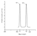
図11のように、発光素子20は、420nm±5nmの主ピーク波長P1を有する青色系列の第1主ピーク波長W1を発光して、前記第1主ピーク波長W1を吸収した第1蛍光体401は470nm±5nmの主ピーク波長P2を青色系列の第2主ピーク波長W2を発光するようになる。前記第2主ピーク波長W1の光度(Intensity)は、前記第1主ピーク波長W1の光度よりさらに低いことがあって、前記第1主ピーク波長W1の光度に比べて70-95%程度の光度を有することができる。
As shown in FIG. 11, the
前記発光素子20は、第1青色波長の光を発光して、前記第1蛍光体401は前記第1青色波長より長波長の第2青色波長の光を発光するようになる。前記第2青色波長は461nm-470nm範囲の主ピーク波長を発光するようになる。
The
前記第1樹脂物402では透光性樹脂系列を含むことができるし、光屈折率と熱特性を考慮してシリコン樹脂またはエポキシ樹脂を含むことができる。前記シリコン樹脂は熱変現象が少なくて、前記発光素子20の高い温度による物性変化が少ない。
The
前記第2樹脂層50は、前記第1樹脂層40の少なくとも一部を覆う形状で形成されることができる。前記第2樹脂層50は第2蛍光体501が第2樹脂物502内に含まれて形成されることができる。前記第2樹脂物502は前記第1樹脂物402と同じくシリコン樹脂またはエポキシ樹脂のような透光性樹脂を含むことができるし、前記第1樹脂層40上に樹脂材質を充填した後、これを硬化する方式で形成されることができる。前記第1樹脂層40の形状は曲面を有する凸型レンズ形状や平たい形状であることができるし、前記第2樹脂層50の形状は曲面を有する凸型レンズ形状や平たい形状であることができる。前記第1及び第2樹脂層40、50の曲面または平たい形状は光が出射される面の形状であることができる。
The
前記第2蛍光体501は、前記発光素子20から放出される第1主ピーク波長の光と前記第1蛍光体401から放出された第2主ピーク波長の光のうちで少なくとも一つを吸収及び励起して第2光を生成することができる。例えば、前記第2蛍光体501で赤色蛍光体、緑色蛍光体、黄色蛍光体のうちで少なくとも一つを含むことができるし、例えば赤色、緑色、黄色蛍光体をすべて含むことができる。前記発光素子20で生成された光が前記第2蛍光体501に入射されて、他の波長の光で発光することができる。前記第2蛍光体501は、青色波長に比べて長波長の光を発光する蛍光体として、YAG、TAG、Silicate、Nitride、Oxynitride系材質のうちで少なくとも一つを含むことができる。
The
前記赤色蛍光体は、La2O2S:Eu3+、Y2O2S:Eu3+、Y2O3:Eu3+(Bi3+)、CaS:Eu2+、(Zn、Cd)S:Ag+(Cl-)、K5(WO4)6.25:Eu3+ 2.5、LiLa2O2BO3:Eu3+のうちで少なくとも一つを含むことができる。緑色蛍光体は、ZnS:Cu+(Al3+)、SrGa2S4:Eu2+、CaMgSi2O7:Eu2+、Ca8Mg(SiO4)Cl2:Eu2+(Mn2+)、(Ba、Sr)2SiO4:Eu2+のうちで少なくとも一つを含むことができる。前記黄色蛍光体は、Y3Al5O12:Ce3+、Sr2SiO4:Eu2+のうちで少なくとも一つを含むことができる。前記赤色蛍光体によって放出された主ピーク波長は、600-630nm範囲内であり、前記緑色蛍光体によって放出された主ピーク波長は、525-535nm範囲内であり、 黄色蛍光体によって放出された主ピーク波長は、510-525nm範囲内にある。前記発光素子20と前記第1蛍光体401によって青色系列の波長が増加することで、第2蛍光体501である黄色、緑、赤色蛍光体による発光効率も増加するようになる。これによって470±10nmの感性照明効果を極大化することができるだけでなく、白色バランスの自由度も増加して、色座標制御を効率的にできる。
The red phosphor includes La 2 O 2 S: Eu 3+ , Y 2 O 2 S: Eu 3+ , Y 2 O 3 : Eu 3+ (Bi 3+ ), CaS: Eu 2+ , (Zn, Cd ) S: Ag + (Cl − ), K 5 (WO 4 ) 6.25 : Eu 3+ 2.5 , LiLa 2 O 2 BO 3 : Eu 3+ The green phosphors are ZnS: Cu + (Al 3+ ), SrGa 2 S 4 : Eu 2+ , CaMgSi 2 O 7 : Eu 2+ , Ca 8 Mg (SiO 4 ) Cl 2 : Eu 2+ (Mn 2+ ), (Ba, Sr) 2 SiO 4 : Eu 2+ . The yellow phosphor may include at least one of Y 3 Al 5 O 12 : Ce 3+ and Sr 2 SiO 4 : Eu 2+ . The main peak wavelength emitted by the red phosphor is in the range of 600-630 nm, the main peak wavelength emitted by the green phosphor is in the range of 525-535 nm, and the main peak wavelength emitted by the yellow phosphor is The peak wavelength is in the 510-525 nm range. As the wavelength of the blue series is increased by the
前記第3樹脂層60は、第2樹脂層50及びキャビティ15を全体的に覆うように形成されることができる。前記第3樹脂層60は本実施例でエポキシまたはシリコン樹脂をモールディングして形成されることができる。前記第2樹脂層50は第1樹脂層40と第3樹脂層60との間に配置される。そして、前記第3樹脂層60は上端の発光面が凸なレンズ型の曲面でなされるか、または平たい形状で形成されることができるし、第1樹脂層40及び第2樹脂層50を経りながら得られた光を外部に放出することができる。前記第3樹脂層60内に第1蛍光体がさらに含まれることができるし、前記第1蛍光体から分離された透光性樹脂層で形成されることができる。
The
前記第1乃至第3樹脂層40、50、60のうちで少なくとも一つの表面は、凹凸面で形成されることができるし、前記凹凸面は光を屈折させて、光指向角を改善させてくれることができる。 At least one surface of the first to third resin layers 40, 50, and 60 may be formed as an uneven surface, and the uneven surface refracts light to improve a light directivity angle. I can give you.
前記第1樹脂層40内の第1蛍光体401の含量は、前記第2樹脂層50内の第2蛍光体の含量と異なるように、例えば、さらに多い含量を有する。
For example, the content of the
前記第1乃至第3樹脂層40、50、60は、透光性樹脂層であり、前記第3樹脂層60は前記第2樹脂層50の屈折率より低い屈折率を有する材質で形成されて、前記第2樹脂層50は前記第1樹脂層40の屈折率より低い屈折率を有する材質で形成されることができる。前記第1乃至第3樹脂層40、50、60の屈折率は2以下、例えば、1.6以下の材質で形成されることができる。ここで、前記第1樹脂層40と前記第2樹脂層50の屈折率は等しいことがあって、これは等しい樹脂材質で形成されることができる。 前記第1蛍光体は、前記胴体10内に添加されることができる。前記胴体10は反射率が70%以上であり、透過率が10%未満であり、前記第1蛍光体は、前記胴体10を透過した光のうちで波長を変化させて461nm-480nmの主ピーク波長を発光することができる。
The first to third resin layers 40, 50 and 60 are translucent resin layers, and the
図2を参考すれば、前記第1蛍光体401に入射した光の角度が変化されて反射することができるし、光を散乱させて発光することができる。
Referring to FIG. 2, the angle of the light incident on the
前記第1蛍光体401の直径が小さければ、光の拡散効果が充分でなくて、過度に増加すれば蛍光体で光が吸収される問題点が発生することができるので、前記第1蛍光体401は、光の吸収を最小化する大きさ、例えば、1乃至10μmの直径を有するように形成されることができる。
If the diameter of the
前記第1蛍光体401は、前記発光素子20で生成された光の相当部分を散乱させることができる。よって、前記第1樹脂層40を通過した光は片方へ偏重されることなしに、均一に混合することができるし、これによって前記第2樹脂層50の上側では色偏差が減少された光が得られることができる。
The
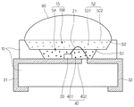
図3は、第2実施例による発光素子パッケージ100Bを示した図面である。前記第2実施例を説明するにおいて、前記第1実施例と等しい部分は同一符号で処理して、重複説明は略することにする。 FIG. 3 is a view illustrating a light emitting device package 100B according to a second embodiment. In the description of the second embodiment, parts that are the same as in the first embodiment are processed with the same reference numerals, and redundant descriptions are omitted.
図3を参照すれば、胴体10のキャビティ15には第1樹脂層40及び第2樹脂層50が配置されて、前記第2樹脂層50の第2樹脂物502内部に第1蛍光体401及び第2蛍光体501が添加される。前記第2樹脂層50に含まれる第1蛍光体401は、第1樹脂層40に含まれた第1蛍光体401とは別に形成されることで、前記第1樹脂層40内の第1蛍光体401と第2樹脂層50内の第1蛍光体401がお互いに異なる樹脂層で461nm-480nm範囲の光を発光することで、青色光を増大させてくれることができるし、感性照明効果を与えることができる。
Referring to FIG. 3, the
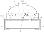
図4は、第3実施例による発光素子パッケージ100Cを示した図面である。前記第3実施例を説明するにおいて、前記第1実施例と等しい部分は同一符号で処理して、重複説明は略することにする。 FIG. 4 illustrates a light emitting device package 100C according to the third embodiment. In the description of the third embodiment, parts that are the same as in the first embodiment are processed with the same reference numerals, and redundant descriptions are omitted.
図4を参照すれば、第3樹脂層60が前記第1樹脂層40及び第2樹脂層50を覆うように形成されることができるし、前記第3樹脂層60の内部に第1蛍光体401が含まれることができる。前記第3樹脂層60の内部に第1蛍光体401が含まれるので、青色波長の光の拡散効果が上昇することができるし、色座標の調節がさらに容易になることができる。
Referring to FIG. 4, the
前記第3樹脂層60の形状が図示したところのように発光素子20に垂直した方向の上に形成される部分の高さが高くて、周辺に行くほど高さが低くなるレンズ形態で形成される場合、前記発光素子20上側に含まれる第1蛍光体401の量が多くなるので、中央に集中された多くの青色光を上部全領域にかけて効果的に散乱させることができる。
As shown in the figure, the
以上でよく見たところのように、前記第1蛍光体401は、前記発光素子20の発光波長に対応する励起波長の値を有するように形成されるので、波長を変化させること以外に光を散乱させることができるし、特に、垂直型発光素子で光が垂直に偏重される現象を改善することができる。
As has been well seen above, the
図5は、第4実施例による発光素子パッケージを示した図面である。前記第4実施例を説明するにおいて、前記第1実施例と等しい部分は同一符号で処理して、重複説明は略することにする。 FIG. 5 illustrates a light emitting device package according to a fourth embodiment. In the description of the fourth embodiment, the same parts as those of the first embodiment are processed with the same reference numerals, and the duplicate description is omitted.
図5を参照すれば、発光素子パッケージは、胴体10、キャビティ15、前記胴体10に配置された第1リード電極31及び第2リード電極32、前記第1リード電極31及び第2リード電極32と電気的に連結されて光を生成する発光素子20、前記発光素子20と前記第2リード電極32を連結するワイヤ21、前記発光素子20を密封するように形成された第1樹脂層41、該第1樹脂層41上に形成された第2樹脂層51、第2樹脂層51及び前記キャビティ15を満たす第3樹脂層60を備えることができる。
Referring to FIG. 5, the light emitting device package includes a
前記第1樹脂層41は、上面S1がフラットな面または平たい面で形成されて、前記第2樹脂層51は上面S2がフラットな面または平たい面で形成されることができる。前記第1樹脂層41は前記第2樹脂層51とキャビティ15の底の間に配置されて、前記第2樹脂層51は前記第1樹脂層41と前記第3樹脂層60との間に配置される。前記第1樹脂層41の上面S1は前記胴体10の上面より低いキャビティ15内に配置されることができるし、これに対して限定しない。
The
前記第1樹脂層41には、第1蛍光体401が形成されて、前記第2樹脂層51には第2蛍光体501が形成される。
A
前記第2樹脂層51の上面S2は、前記胴体10の上面と同一平面上に配置されるか、または他の平面上に配置されることができる。
The upper surface S2 of the
図6は、第5実施例による発光素子パッケージを示した図面である。前記第5実施例を説明するにおいて、前記第1実施例と等しい部分は同一符号で処理して、重複説明は略することにする。 FIG. 6 illustrates a light emitting device package according to a fifth embodiment. In the description of the fifth embodiment, parts that are the same as in the first embodiment are processed with the same reference numerals, and redundant descriptions are omitted.
図6を参照すれば、発光素子パッケージは、胴体10、キャビティ15、前記胴体10に配置された第1リード電極31及び第2リード電極32、前記第1リード電極31及び第2リード電極32と電気的に連結されて光を生成する発光素子20、前記発光素子20と前記第2リード電極32を連結するワイヤ21、前記発光素子20を密封するように形成された第1樹脂層42、前記第1樹脂層42上に形成された第2樹脂層52、第2樹脂層52及び前記キャビティ15を満たす第3樹脂層60を備えることができる。
Referring to FIG. 6, the light emitting device package includes a
前記キャビティ15は、第1樹脂層42が配置された第1キャビティブ15Aと第2樹脂層52が形成された第2キャビティブ15Bを含む。前記第1キャビティブ15Aの上部幅は、前記第2キャビティブ15Bの上部幅より狭く形成されることができる。これは前記キャビティ15の内部側面らが2段以上の段差になった構造で形成されることができる。また、第1キャビティブ15Aの側面と前記第2キャビティブ15Bとの側面らは、お互いに異なる角度で傾くように形成されることができるし、これに対して限定しない。
The
図7は、第6実施例による発光素子パッケージを示した図面である。前記第6実施例を説明するにおいて、前記第1実施例と等しい部分は同一符号で処理して、重複説明は略することにする。 FIG. 7 illustrates a light emitting device package according to a sixth embodiment. In the description of the sixth embodiment, parts that are the same as in the first embodiment are processed with the same reference numerals, and redundant descriptions are omitted.
図7を参照すれば、発光素子パッケージは、胴体10、キャビティ15、前記胴体10に配置された第1リード電極31及び第2リード電極32、前記第1リード電極31及び第2リード電極32と電気的に連結されて光を生成する発光素子20、該発光素子20と前記第2リード電極32を連結するワイヤ21、前記発光素子20を密封するように形成された第1樹脂層41A、前記第1樹脂層41A上に形成された第2樹脂層51A、第2樹脂層51A及び前記キャビティ15を満たす第3樹脂層60を含むことができる。
Referring to FIG. 7, the light emitting device package includes a
前記第1樹脂層41Aには第1樹脂物402内に第1蛍光体401及び第2蛍光体502が添加されることができる。図11のように、前記発光素子20は420nm±5nm範囲の主ピーク波長を有する青色系列の第1主ピーク波長W1を発光して、前記第1主ピーク波長W1を吸収した第1蛍光体401は470nm±5nmの主ピーク波長P2を青色系列の第2主ピーク波長W2を発光するようになる。前記第2主ピーク波長W2の光度(Intensity)は前記第1主ピーク波長W1の光度よりさらに低いことがあって、前記第1主ピーク波長W1の光度に比べて70-95%程度の光度を有することができる。
A
前記第2蛍光体501は、前記発光素子20から放出される第1主ピーク波長の光と前記第1蛍光体401から放出された第2主ピーク波長の光のうちで少なくとも一つを吸収及び励起して第2光を生成することができる。例えば、前記第2蛍光体501で赤色蛍光体、緑色蛍光体、黄色蛍光体のうちで少なくとも一つを含むことができるし、例えば赤色、緑色、黄色蛍光体をすべて含むことができる。
The
前記第1樹脂層41Aを通じてお互いに異なる主ピーク波長を有する青色と、510nm以上のピーク波長を有する第2カラーを放出されることができる。
Through the
前記第2樹脂層51Aは、他の蛍光体らから分離されて、どのような蛍光体を持たない透光性樹脂層で定義することができる。
The
図8は、第7実施例による発光素子パッケージを示した図面である。前記第7実施例を説明するにおいて、前記第1実施例と等しい部分は同一符号で処理して、重複説明は略することにする。 FIG. 8 is a view illustrating a light emitting device package according to a seventh embodiment. In the description of the seventh embodiment, parts that are the same as in the first embodiment are processed with the same reference numerals, and redundant descriptions are omitted.
図8を参照すれば、発光素子パッケージは胴体10、キャビティ15、前記胴体10に配置された第1リード電極31及び第2リード電極32、前記第1リード電極31及び第2リード電極32と電気的に連結されて光を生成する発光素子20、前記発光素子20と前記第2リード電極32を連結するワイヤ21、前記発光素子20を密封するように形成された第1樹脂層41B、前記第1樹脂層41B上に形成された第2樹脂層51B、第2樹脂層51B及び前記キャビティ15を満たす第3樹脂層60を備えることができる。
Referring to FIG. 8, the light emitting device package includes a
前記第1樹脂層41Bにはどのような蛍光体を持たない透光性樹脂層で形成される。
The
前記第2樹脂層51Bには、第2樹脂物502内に第1蛍光体401及び第2蛍光体502が添加されることができる。前記発光素子20は、420nmの主ピーク波長を有する青色系列の第1主ピーク波長W1を発光して、前記第1主ピーク波長W1を吸収した第1蛍光体401は470nm±5nmの主ピーク波長P2を青色系列の第2主ピーク波長W2を発光するようになる。前記第2主ピーク波長W2の光度(Intensity)は前記第1主ピーク波長W1の光度よりさらに低いことがあって、前記第1主ピーク波長W1の光度に比べて70-95%程度の光度を有することができる。
A
前記第2蛍光体501は、前記発光素子20から放出される第1主ピーク波長の光と前記第1蛍光体401から放出された第2主ピーク波長の光のうちで少なくとも一つを吸収及び励起して第2光を生成することができる。例えば、前記第2蛍光体501で赤色蛍光体、緑色蛍光体、黄色蛍光体のうちで少なくとも一つを含むことができるし、例えば赤色、緑色、黄色蛍光体をすべて含むことができる。
The
前記第2樹脂層51Bを通じてお互いに異なる主ピーク波長を有する青色と、510nm以上のピーク波長を有する第2カラーを放出されることができる。
Through the
図9は、第8実施例による発光素子パッケージを示した図面であり、図10は図9の発光素子パッケージの側断面図である。前記第8実施例を説明するにおいて、前記第1実施例と等しい部分は同一符号で処理して、重複説明は略することにする。 FIG. 9 is a view showing a light emitting device package according to an eighth embodiment, and FIG. 10 is a side sectional view of the light emitting device package of FIG. In the description of the eighth embodiment, parts that are the same as in the first embodiment are processed with the same reference numerals, and redundant descriptions are omitted.
図9及び図10を参照すれば、発光素子パッケージは、第1キャビティ17を有する胴体12、第2キャビティ34を有する第1リード電極33、第3キャビティ36を有する第2リード電極35、連結フレーム38、発光チップら22、23、及びワイヤら25乃至28を含む。
9 and 10, the light emitting device package includes a
胴体12は、ポリフタルアミド(PPA:Polyphthalamide)のような樹脂材質、シリコン(Si)、金属材質、PSG(photo sensitive glass)、サファイア(Al2O3)、印刷回路基板(PCB)のうちで少なくとも一つで形成されることができる。望ましくは、胴体12は、ポリフタルアミド(PPA:Polyphthalamide)のようなプラスチック樹脂材質とシリコン材質のうちで少なくとも一つでなされることができる。
The
胴体12の上面形状は、発光素子パッケージの用途及び設計によって三角形、四角形、多角形、及び円形など多様な形状を有することができる。前記第1リード電極33及び第2リード電極35は、胴体12の底に配置されて直下タイプで基板上に搭載されることができるし、前記胴体12の側面に配置されてエッジタイプで基板上に搭載されることができるし、これに対して限定しない。
The upper surface of the
胴体12は上部が開放されて、側面と底でなされた第1キャビティ(cavity)17を有する。前記第1キャビティ17は前記胴体12の上面から凹なコップ構造またはリセス構造を含むことができるし、これに対して限定しない。第1キャビティ17の側面は底に対して垂直するか、または傾くことができる。
The
第1キャビティ17を上で眺めた形状は円形、卵円形、多角形(例えば、四角形)であることがある。第1キャビティ17の角は曲面や、平面であることができる。
The shape of the
前記第1リード電極33は前記第1キャビティ17の第1領域に配置されて、前記第1キャビティ17の底に一部が配置されてその中心部に前記第1キャビティ17の底よりさらに低い深さを有するように凹な第2キャビティ34が配置される。前記第2キャビティ34は、前記第1リード電極33の上面から前記胴体12の下面方向に凹な形状、例えば、コップ(Cup)構造、またはリセス(recess)形状を含む。前記第2キャビティ34の側面は、前記第2キャビティ34の底から傾くか、または垂直するように折曲されることができる。前記第2キャビティ34の側面のうちで対向される二つの側面は等しい角度で傾くか、またはお互いに異なる角度で傾くことができる。
The
前記第2リード電極35は、前記第1キャビティ17の第1領域と離隔される第2領域に配置されて、前記第1キャビティ17の底に一部が配置されて、その中心部には前記第1キャビティ17の底よりさらに低い深さを有するように凹な第3キャビティ36が形成される。前記第3キャビティ36は、前記第2リード電極113の上面から前記胴体12の下面方向に凹な形状、例えば、コップ(Cup)構造またはリセス(recess)形状を含む。前記第3キャビティ36の側面は、前記第3キャビティ36の底から傾くか、または垂直するように折曲されることができる。前記第3キャビティ36の側面のうちで対向される二つの側面は等しい角度で傾くか、またはお互いに異なる角度で傾くことができる。
The
前記第1リード電極33の上部は、前記胴体12のセンター領域で前記第2リード電極35の上部とお互いに対応されるように配置されて、これに対して限定しない。
The upper part of the
前記第1リード電極33の下面及び前記第2リード電極35の下面前記胴体12の下面に露出するか、または前記胴体12の下面と同一平面上に配置されることができる。
The lower surface of the
前記第1リード電極33の第1リード部33Aは前記胴体12の下面に配置されて、前記胴体12の第1側面113に突き出されることができる。前記第2リード電極35の第2リード部35Aは前記胴体12の下面に配置されて前記胴体12の第1側面の反対側第2側面114に突き出されることができる。
The
前記連結フレーム38は、前記第1リード電極33と前記第2リード電極35との間の領域一側に配置されて、前記胴体12の第1側面111に接するように配置される。前記連結フレーム38は前記第1発光チップ22と第2発光チップ23をお互いに連結させてくれる。
The
前記第1リード電極33、前記第2リード電極35及び前記連結フレーム38は金属材質、例えば、チタン(Ti)、銅(Cu)、ニッケル(Ni)、金(Au)、クロム(Cr)、タンタル(Ta)、白金(Pt)、スズ(Sn)、銀(Ag)、燐(P)のうちで少なくとも一つを含むことができるし、単一金属層または多層金属層で形成されることができる。前記第1、第2リード電極33、35及び連結フレーム38の厚さは等しい厚さで形成されることができるし、これに対して限定しない。
The
前記第2キャビティ34及び前記第3キャビティ36の底形状は直四角形、正四角形または曲面を有する円または楕円形状であることができる。
The bottom shape of the
前記第1リード電極33の第2キャビティ34内には第1発光チップ22が配置されて、前記第2リード電極31の第3キャビティ36内には第2発光チップ23が配置されることができる。
The first
前記第1発光チップ23は、第1及び第2ワイヤ25、26で前記第1キャビティ17の底に配置された第1リード電極33と連結フレーム38に連結されることができる。前記第2発光チップ25は、第1及び第2ワイヤ27、28で前記連結フレーム38と前記第1キャビティ17の底に配置された第1リード電極33に連結されることができる。
The first
前記第1キャビティ17内の所定領域には、保護素子が配置されることができるし、前記保護素子はサイリスター、ツェナーダイオード、またはTVS(Transient voltage suppression)で具現されることができるし、前記ツェナーダイオードは前記発光チップをESD(electro static discharge)から保護するようになる。
A protective element may be disposed in a predetermined region of the
前記発光素子22、23は、III族乃至V族元素の化合物半導体を含んで、青色波長、例えば、410nm-460nm範囲の波長を発光するようになる。第1発光素子22は、410nm-460nmのうちで410nm-440nm範囲の主ピーク波長を発光することができるし、前記第2発光素子23は前記第1発光素子22の主ピーク波長と異なる主ピーク波長、例えば、430nm-460nm範囲の主ピーク波長を発光することができる。
The
他の例として、前記第1発光素子22及び第2発光素子23は、主ピーク波長が同じか、または少なくとも1nmの波長差を有する主ピーク波長で発光することができる。
As another example, the first
前記胴体12の第2キャビティ34には、第1樹脂層43が形成されて、第3キャビティ36には第2樹脂層44が配置されて、前記第1キャビティ17には第3樹脂層53が形成される。
A
前記第1樹脂層43は、第1樹脂物404及び前記第1樹脂物404内に添加された第1蛍光体403を含む。前記第2樹脂層44は第2樹脂物406及び前記第1樹脂物406内に添加された第2蛍光体405を含む。前記第3樹脂層53は第3樹脂物504及び前記第3樹脂物504内に第3蛍光体503を含む。前記第1乃至第3樹脂物404、406、504はシリコンまたはエポキシのような透光性樹脂材質で形成されることができる。
The
前記第1蛍光体403は青色蛍光体であり、前記青色蛍光体は、例えば、Sr2MgSi2O7:Eu2+、BaMgAl10O17:Eu(Mn)、Sr5Ba3MgSi2O8:Eu2+、Sr2P2O7:Eu2+、SrSiAl2O3N2:Eu2+、(Ba1-xSrx)SiO4:Eu2+、(Sr、Ca、Ba、Mg)10(PO4)6Cl2:Eu2+、CaMgSi2O6:Eu2+のうちで少なくとも一つを含むことができる。
The
前記第2蛍光体405は青色蛍光体であり、前記青色蛍光体は、例えば、Sr2MgSi2O7:Eu2+、BaMgAl10O17:Eu(Mn)、Sr5Ba3MgSi2O8:Eu2+、Sr2P2O7:Eu2+、SrSiAl2O3N2:Eu2+、(Ba1-xSrx)SiO4:Eu2+、(Sr、Ca、Ba、Mg)10(PO4)6Cl2:Eu2+、CaMgSi2O6:Eu2+のうちで少なくとも一つを含むことができる。
The
前記第1蛍光体403は、前記第1発光素子22から放出された410nm-440nm範囲の光を励起して青色波長範囲、例えば、465nm-475nm範囲の主ピーク波長で発光することができる。前記第2蛍光体405は前記第2発光素子23から放出された430nm-460nm範囲の光を励起して青色波長範囲、例えば、469nm-479nm範囲で発光することができる。前記第2蛍光体405の主ピーク波長は前記第1蛍光体403より長波長の光を発光することができる。
The
他の例として、前記第1及び第2発光素子22、23は410-440nm範囲で発光するか、または430nm-460nm範囲で発光することができる。この場合、前記第1蛍光体403は前記第1発光素子22から放出された光を励起して青色波長範囲、例えば、465nm-475nm範囲の主ピーク波長で発光することができる。前記第2蛍光体405は前記第2発光素子23から放出された410nm-460nm範囲の光を励起して青色波長範囲、例えば、469nm-479nm範囲で発光することができる。前記第2蛍光体405の主ピーク波長は前記第1蛍光体403より長波長の光を発光することができる。
As another example, the first and second
前記第1蛍光体403及び第2蛍光体405は、前記第1及び第2発光素子22、23の主ピーク波長より長波長の光を発光するようになる。前記第1及び第2蛍光体403、405の発光波長と前記第1及び第2発光素子22、23の発光波長の差は5nm-69nmであることがある。
The
前記第3蛍光体503は、赤色蛍光体、黄色蛍光体、及び緑色蛍光体のうちで少なくとも一つを含むことができる。前記第3蛍光体503は、前記第1発光素子22、第2発光素子23、第1蛍光体403、第2蛍光体405から発光された光の一部を励起して青色波長より長波長の光を発光するようになる。前記第3樹脂物504内に第1蛍光体さらに添加されることができる。
The
前記第1及び第2蛍光体403、405の発光波長が前記発光素子22、23の発光波長範囲とマッチングされる値を有するように形成された場合、前記発光素子22、23で生成された光と前記第1及び第2蛍光体403、405から発光された光によって青色成分が他の波長の値を有する光に比べて相対的にさらにたくさん発光されるようにすることで、色座標の値を維持しながら白色光効率を高めることができる。また470nm±5nm範囲の波長の成分を発光することで、感性照明効果を極大化することができるし、カラーホワイトバランスの自由度が増大されて色座標制御が容易なことがある。
When the emission wavelengths of the first and
前記胴体12の上部には、レンズがさらに形成されることができるし、前記レンズは凹型または/及び凸型レンズの構造を含むことができるし、発光素子が放出する光の配光(lightdistribution)を調節することができる。
A lens may be further formed on the
前記実施例は、発光素子パッケージのお互いに異なる領域に2個のキャビティを有する構造で説明したが、3個以上のキャビティがお互いに異なる領域に配置されることができる。また、発光素子パッケージ内に2個の発光素子に対して説明したが、3個以上の発光素子が配置されることができるし、これに対して限定しない。 The embodiment has been described with the structure having two cavities in different regions of the light emitting device package, but three or more cavities may be disposed in different regions. Further, although two light emitting elements have been described in the light emitting element package, three or more light emitting elements can be disposed, and the present invention is not limited thereto.
図12は、実施例による発光素子を示した図面である。 FIG. 12 is a view illustrating a light emitting device according to an embodiment.
図12を参照すれば、発光素子20は発光構造物110、発光構造物110下にオーミック層121が形成されて、前記オーミック層121下に反射層124が形成されて、前記反射層124下に伝導性支持部材125が形成されて、前記反射層124と前記発光構造物110のまわりに保護層123が形成されることができる。
Referring to FIG. 12, the
前記発光構造物110は、第1導電型半導体層113、第2導電型半導体層115及び前記第1導電型半導体層113と前記第2導電型半導体層115との間に活性層114が形成される。
The
前記第1導電型半導体層113は、第1導電型ドーパントがドーピングされた3族-5族元素の化合物半導体、例えば、GaN、AlN、AlGaN、InGaN、InN、InAlGaN、AlInN、AlGaAs、GaP、GaAs、GaAsP、AlGaInPなどで選択されることができる。前記第1導電型がN型半導体の場合、前記第1導電型ドーパントはSi、Ge、Sn、Se、TeなどのようなN型ドーパントを含む。前記第1導電型半導体層114は単層または多層で形成されることができるし、これに対して限定しない。
The first conductive
前記活性層114は、単一量子井構造、多重量子井構造、量子線構造、量子点構造で形成されることができる。前記活性層114は3族-5族元素の化合物半導体材料を利用して井戸層と障壁層の周期、例えば、InGaN井戸層/GaN障壁層またはInGaN井戸層/AlGaN障壁層の周期で形成されることができる。前記活性層114の井戸層は410-460nmの主ピーク波長のために、インジウム含量を3-15%範囲を有することができる。前記井戸層のインジウム含量を低める場合、長波長よりは短波長範囲に移動するようになる。
The
前記活性層114の上または/及び下には導電型クラッド層が形成されることができるし、前記導電型クラッド層はAlGaN系半導体で形成されることができる。
A conductive clad layer may be formed on and / or below the
前記活性層114の下には前記第2導電型半導体層115が形成されて、前記第2導電型半導体層115は、第2導電型ドーパントがドーピングされた3族-5族元素の化合物半導体、例えば、GaN、AlN、AlGaN、InGaN、InN、InAlGaN、AlInN、AlGaAs、GaP、GaAs、GaAsP、AlGaInPなどで選択されることができる。前記第2導電型がP型半導体の場合、前記第2導電型ドーパントはMg、ZeなどのようなP型ドーパントを含む。前記第2導電型半導体層115は単層または多層で形成されることができるし、これに対して限定しない。
The second
また、前記第2導電型半導体層115の下には第3導電型半導体層、例えば、N型半導体層が形成されることができる。前記発光構造物135はN-P接合、P-N接合、N-P-N接合、P-N-P接合構造のうちで少なくとも一つが形成されることができる。
A third conductive semiconductor layer, for example, an N-type semiconductor layer may be formed under the second
前記オーミック層121は、発光構造物110の下層、例えば第2導電型半導体層115にオーミック接触されて、その材料はITO(indium tin oxide)、IZO(indium zin coxide)、IZTO(indium zinc tin oxide)、IAZO(indium aluminum zinc oxide)、IGZO(indium gallium zinc oxide)、IGTO(indium gallium tin oxide)、AZO(aluminum zinc oxide)、ATO(antimony tin oxide)、GZO(gallium zinc oxide)、Ag、Ni、Al、Rh、Pd、Ir、Ru、Mg、Zn、Pt、Au、Hf及びこれらの選択的な組合で構成された物質のうちで形成されることができる。また、前記金属物質とIZO、IZTO、IAZO、IGZO、IGTO、AZO、ATOなどの透光性伝導性物質を利用して多層で形成することができるし、例えば、IZO/Ni、AZO/Ag、IZO/Ag/Ni、AZO/Ag/Niなどで積層することができる。前記オーミック層121内部は電極116と対応されるように電流をブロッキングする層がさらに形成されることができる。
The
前記保護層123は、ITO(indium tin oxide)、IZO(indium zinc oxide)、IZTO(indium zinc tin oxide)、IAZO(indium aluminum zinc oxide)、IGZO(indium gallium zinc oxide)、IGTO(indium gallium tin oxide)、AZO(aluminum zinc oxide)、ATO(antimony tin oxide)、GZO(gallium zinc oxide)、SiO2、SiOx、SiOxNy、Si3N4、Al2O3、TiO2程度で選択的に形成されることができる。前記保護層123は、スパッタリング方法または蒸着方法などを利用して形成することができるし、反射層124のような金属が発光構造物110の層らをショートさせることを防止することができる。
The protective layer 123 is made of ITO (indium tin oxide), IZO (indium zinc oxide), IZTO (indium zinc tin oxide), IAZO (indium aluminum zinc oxide), IGZO (indium gallium zinc oxide), IGTO (indium gallium tin oxide). ), AZO (aluminum zinc oxide), ATO (antimony tin oxide), GZO (gallium zinc oxide), SiO 2 , SiOx, SiOxNy, Si 3 N 4 , Al 2 O 3 , and TiO 2. be able to. The protective layer 123 can be formed using a sputtering method, an evaporation method, or the like, and can prevent a metal such as the reflective layer 124 from shorting the layers of the
前記反射層124は、Ag、Ni、Al、Rh、Pd、Ir、Ru、Mg、Zn、Pt、Au、Hf及びこれらの選択的な組合で構成された物質で形成されることができる。前記反射層124は前記発光構造物110の幅より大きく形成されることができるし、これは光反射効率を改善させてくれることができる。
The reflective layer 124 may be formed of a material composed of Ag, Ni, Al, Rh, Pd, Ir, Ru, Mg, Zn, Pt, Au, Hf, and a selective combination thereof. The reflective layer 124 may be formed larger than the width of the
前記伝導性支持部材125は、ベース基板として、銅(Cu)、金(Au)、ニッケル(Ni)、モリブデン(Mo)、銅-タングステン(Cu-W)、キャリアウェハー(例:Si、Ge、GaAs、ZnO、SiCなど)などで具現されることができる。前記伝導性支持部材125と前記反射層124との間には接合層がさらに形成されることができるし、前記接合層は二つの層をお互いに接合させてくれることができる。
The
前記開示された発光チップは一例であり、前記に開示された特徴に限定しない。前記発光チップは、前記の発光素子の実施例に選択的に適用されることができるし、これに対して限定しない。 The disclosed light emitting chip is an example, and is not limited to the above disclosed features. The light emitting chip can be selectively applied to the embodiment of the light emitting device, but is not limited thereto.
本発明の一実施例による発光素子パッケージは、照明システムに適用されることができる。前記照明システムは複数の発光素子パッケージがアレイされた構造を含んで、図13及び図14に示された表示装置、図15に示された照明装置を含んで、照明灯、信号灯、車両ヘッドライト、電光板、指示灯のようなユニットに適用されることができる。 The light emitting device package according to an embodiment of the present invention may be applied to a lighting system. The lighting system includes a structure in which a plurality of light emitting device packages are arrayed. The lighting system includes the display device shown in FIGS. 13 and 14, and the lighting device shown in FIG. It can be applied to units such as lightning boards and indicator lights.
図13は、本発明の一実施例による表示装置の分解斜視図である。 FIG. 13 is an exploded perspective view of a display device according to an embodiment of the present invention.
図13を参照すれば、表示装置1000は、導光板1041と、該導光板1041に光を提供する発光モジュール1031と、前記導光板1041下に反射部材1022と、前記導光板1041上に光学シート1051と、該光学シート1051上に表示パネル1061と、前記導光板1041、発光モジュール1031及び反射部材1022を収納するボトムカバー1011とを備えることができるが、これに限定されない。
Referring to FIG. 13, the
前記ボトムカバー1011、反射シート1022、導光板1041、光学シート1051は、ライトユニット1050で定義されることができる。
The
前記導光板1041は、前記発光モジュール1031から提供された光を拡散させて面光源化させる役割をする。前記導光板1041は、透明な材質でなされて、例えば、PMMA(polymethyl metaacrylate)のようなアクリル樹脂系列、PET(polyethylene terephthlate)、PC(poly carbonate)、COC(cycloolefin copolymer)及びPEN(polyethylene naphthalate)樹脂のうちで一つを含むことができる。
The
前記発光モジュール1031は、前記導光板1041の少なくとも一側面に配置されて、前記導光板1041の少なくとも一側面に光を提供して、窮極的には表示装置の光源として作用するようになる。
The
前記発光モジュール1031は、前記ボトムカバー1011内に少なくとも一つが配置されて、前記導光板1041の一側面で直接または間接的に光を提供することができる。前記発光モジュール1031は基板1033と前記に開示された実施例による発光素子パッケージ100を含んで、前記発光素子パッケージ100は前記基板1033上に所定間隔でアレイされることができる。前記基板は印刷回路基板(printed circuit board)であることがあるが、これに限定しない。また、前記基板1033はメタルコアPCB(MCPCB、Metal Core PCB)、軟性PCB(FPCB、Flexible PCB)などを含むこともでき、これに対して限定しない。前記発光素子パッケージ100は、前記ボトムカバー1011の側面または放熱プレート上に搭載される場合、前記基板1033は除去されることができる。前記放熱プレートの一部は前記ボトムカバー1011の上面に接触されることができる。よって、発光素子パッケージ100で発生された熱は放熱プレートを経由してボトムカバー1011に放出されることができる。
At least one light emitting
前記複数の発光素子パッケージ100は、前記基板1033上に光が放出される出射面が前記導光板1041と所定距離離隔されるように搭載されることができるし、これに対して限定しない。前記発光素子パッケージ100は、前記導光板1041の一側面である入光部に光を直接または間接的に提供することができるし、これに対して限定しない。
The plurality of light emitting device packages 100 may be mounted on the substrate 1033 so that an emission surface from which light is emitted is separated from the
前記導光板1041の下には前記反射部材1022が配置されることができる。前記反射部材1022は前記導光板1041の下面に入射された光を反射させて前記表示パネル1061に供給することで、前記表示パネル1061の輝度を向上させることができる。前記反射部材1022は、例えば、PET、PC、PVCレジンなどで形成されることができるが、これに対して限定しない。前記反射部材1022は前記ボトムカバー1011の上面であることができるし、これに対して限定しない。
The
前記ボトムカバー1011は、前記導光板1041、発光モジュール1031及び反射部材1022などを収納することができる。このために、前記ボトムカバー1011は上面が開口されたボックス(box)形状を有する収納部1012が具備されることができるし、これに対して限定しない。前記ボトムカバー1011はトップカバー(図示せず)と結合されることができるし、これに対して限定しない。
The
前記ボトムカバー1011は、金属材質または樹脂材質で形成されることができるし、プレス成形または圧出成形などの工程を利用して製造されることができる。また、前記ボトムカバー1011は熱伝導性が良い金属または非金属材料を含むことができるし、これに対して限定しない。
The
前記表示パネル1061は、例えば、LCDパネルとして、お互いに対向される透明な材質の第1及び第2基板、そして第1及び第2基板の間に介された液晶層を含む。前記表示パネル1061の少なくとも一面には偏光板が付着することができるし、このような偏光板の付着構造に限定しない。前記表示パネル1061は前記発光モジュール1031から提供された光を透過または遮断させて情報を表示するようになる。このような表示装置1000は、各種携帯端末機、ノートブックコンピューターのモニター、ラップトップコンピューターのモニター、テレビのような映像表示装置に適用されることができる。
The display panel 1061, for example, as an LCD panel, includes first and second substrates made of transparent materials facing each other, and a liquid crystal layer interposed between the first and second substrates. A polarizing plate can be attached to at least one surface of the display panel 1061, and the present invention is not limited to such a polarizing plate attachment structure. The display panel 1061 displays information by transmitting or blocking light provided from the
前記光学シート1051は、前記表示パネル1061と前記導光板1041との間に配置されて、少なくとも一枚以上の透光性シートを含む。前記光学シート1051は、例えば拡散シート(diffusion sheet)、水平及び垂直プリズムシート(horizontal/vertical prism sheet)、及び輝度強化シート(brightness enhanced sheet)などのようなシートのうちで少なくとも一つを含むことができる。前記拡散シートは、入射される光を拡散させてくれて、前記水平または/及び垂直プリズムシートは入射される光を前記表示パネル1061に集光させてくれて、前記輝度強化シートは損失される光を再使用して輝度を向上させてくれる。また、前記表示パネル1061上には保護シートが配置されることができるし、これに対して限定しない。
The optical sheet 1051 is disposed between the display panel 1061 and the
前記発光モジュール1031の光経路上には光学部材として、前記導光板1041、及び光学シート1051を含むことができるし、これに対して限定しない。
The
図14は、本発明の一実施例による発光素子パッケージを有する表示装置を示した図面である。 FIG. 14 is a view illustrating a display device having a light emitting device package according to an embodiment of the present invention.
図14を参照すれば、表示装置1100は、ボトムカバー1152、前記開示発光素子パッケージ100がアレイされた基板1120、光学部材1154、及び表示パネル1155を備える。
Referring to FIG. 14, the
前記基板1120と前記発光素子パッケージ100とは、発光モジュール1060に定義されることができる。前記ボトムカバー1152、少なくとも一つの発光モジュール1060、光学部材1154はライトユニット1150で定義されることができる。
The substrate 1120 and the light emitting
前記ボトムカバー1152には、収納部1153を具備することができるし、これに対して限定しない。
The
前記光学部材1154は、レンズ、導光板、拡散シート、水平及び垂直プリズムシート、及び輝度強化シートなどで少なくとも一つを含むことができる。前記導光板は、PC材質またはPMMA(Poly methy methacrylate)材質でなされることができるし、このような導光板は除去されることができる。前記拡散シートは入射される光を拡散させてくれて、前記水平及び垂直プリズムシートは入射される光を前記表示パネル1155に集光させてくれて、前記輝度強化シートは損失される光を再使用して輝度を向上させてくれる。
The
前記光学部材1154は、前記発光モジュール1060上に配置されて、前記発光モジュール1060から放出された光を面光源するか、または拡散、集光などを遂行するようになる。
The
図15は、本発明の一実施例による照明装置の斜視図である。 FIG. 15 is a perspective view of a lighting device according to an embodiment of the present invention.
図15を参照すれば、照明装置1500はケース1510と、該ケース1510に設置された発光モジュール1530と、前記ケース1510に設置されて外部電源から電源の提供を受ける連結端子1520を備えることができる。
Referring to FIG. 15, the
前記ケース1510は、放熱特性が良好な材質で形成されることが望ましくて、例えば、金属材質または樹脂材質で形成されることができる。
The
前記発光モジュール1530は、基板1532と、該基板1532に搭載される実施例による発光素子パッケージ100を含むことができる。前記発光素子パッケージ100は、複数個がマトリックス形態または所定間隔で離隔されてアレイされることができる。
The light emitting module 1530 may include a substrate 1532 and a light emitting
前記基板1532は、絶縁体に回路パターンが印刷されたものであることができるし、例えば、一般印刷回路基板(PCB:Printed Circuit Board)、メタルコア(Metal Core)PCB、軟性(Flexible)PCB、セラミックスPCB、FR-4基板などを含むことができる。 The substrate 1532 may be a circuit pattern printed on an insulator, such as a general printed circuit board (PCB), a metal core PCB, a flexible PCB, ceramics, and the like. PCB, FR-4 substrate and the like can be included.
また、前記基板1532は、光を効率的に反射する材質で形成されるか、または表面の光が効率的に反射するカラー、例えば、白色、シルバーなどのコーティング層になることがある。 Further, the substrate 1532 may be formed of a material that efficiently reflects light, or may be a coating layer of a color that efficiently reflects light on the surface, such as white or silver.
前記基板1532上には、少なくとも一つの発光素子パッケージ100が搭載されることができる。前記発光素子パッケージ100それぞれは少なくとも一つのLED(LED:Light Emitting Diode)チップを含むことができる。前記LEDチップは、赤色、緑色、青色または白色などのような刺光線範囲の発光ダイオードまたは紫外線(UV:Ultra Violet)を発光するUV発光ダイオードを含むことができる。
At least one light emitting
前記発光モジュール1530は、色感及び輝度を得るために多様な発光素子パッケージ100の組合を有するように配置されることができる。例えば、その演色性(CRI)を確保するために白色発光ダイオード、赤色発光ダイオード及び緑発光ダイオードを組み合わせて配置することができる。 The light emitting module 1530 may be disposed to have various combinations of the light emitting device packages 100 in order to obtain color and brightness. For example, a white light emitting diode, a red light emitting diode, and a green light emitting diode can be arranged in combination in order to ensure the color rendering properties (CRI).
前記連結端子1520は、前記発光モジュール1530と電気的に連結されて電源を供給することができる。前記連結端子1520はソケット方式で外部電源に回して挟まれて結合されるが、これに対して限定しない。例えば、前記連結端子1520はピン(pin)形態で形成されて外部電源に挿入されるか、または配線によって外部電源に連結されることもできるものである。
The
以上で説明したところのように、本発明の一実施例による照明システムは、実施例による発光素子または発光素子パッケージを含むことで光効率が向上させてくれることができるし、感性照明に効果的であることがある。 As described above, the lighting system according to the embodiment of the present invention can improve the light efficiency by including the light emitting device or the light emitting device package according to the embodiment, and is effective for the sensitive lighting. It may be.
以上で本発明の実施例に説明された特徴、構造、効果などは本発明の少なくとも一つの実施例に含まれて、必ず一つの実施例のみに限定されるものではない。延いては、各実施例で例示された特徴、構造、効果などは実施例らが属する分野の通常の知識を有する者によって他の実施例らに対しても組合または変形されて実施可能である。したがって、このような組合と変形に係る内容らは、本発明の範囲に含まれるものとして解釈されなければならないであろう。 また、以上で本発明の実施例を中心に説明したが、これは単に例示であるだけで、本発明を限定するものではなくて、本発明が属する分野の通常の知識を持った者なら本実施例の本質的な特性を脱しない範囲で以上に例示されないさまざまの変形と応用が可能であることが分かることができるであろう。例えば、実施例に具体的に現われた各構成要素は、変形して実施することができるものである。そして、このような変形と応用に係る差異らは添付された請求範囲で規定する本発明の範囲に含まれるものとして解釈されなければならないであろう。 The features, structures, effects, and the like described in the embodiments of the present invention are included in at least one embodiment of the present invention, and are not necessarily limited to only one embodiment. As a result, the features, structures, effects, etc. exemplified in each embodiment can be combined or modified with respect to other embodiments by those having ordinary knowledge in the field to which the embodiments belong. . Accordingly, the contents related to such combinations and modifications should be construed as being included in the scope of the present invention. Further, the embodiments of the present invention have been described above. However, this is merely an example, and is not intended to limit the present invention. Those who have ordinary knowledge in the field to which the present invention belongs will be described. It will be understood that various modifications and applications not described above are possible without departing from the essential characteristics of the embodiments. For example, each component specifically shown in the embodiments can be implemented by being modified. Such variations and modifications should be construed as being included within the scope of the present invention as defined in the appended claims.
Claims (23)
前記胴体に配置された第1リード電極及び第2リード電極と、
前記キャビティ内に配置されて、前記第1リード電極及び第2リード電極のうちの少なくとも1つと電気的に連結されて、420nm乃至460nm範囲の第1ピーク波長の光を発光する発光素子と、
前記発光素子上に第1蛍光体を有する第1樹脂層と、
前記第1樹脂層の上に第2樹脂層と、を備え、
前記第1ピーク波長の一部光が、前記第1蛍光体を励起させて461nm乃至480nm範囲の第2ピーク波長の光を発光し、
前記第1ピーク波長と前記第2ピーク波長は、紫外線より長波長であり、等しい青色帯域の光を含み、
前記第2ピーク波長の光の強度は、前記第1ピーク波長の光の強度の70%乃至95%であり、
前記第2ピーク波長と前記第1ピーク波長の差は45nm乃至55nmの範囲であり、
前記第2樹脂層内に、前記第1蛍光体または第2蛍光体のいずれか1つの蛍光体をさらに含み、
前記第2蛍光体は、赤色蛍光体、緑色蛍光体及び黄色蛍光体のうちの少なくとも1つを含む発光素子パッケージ。 A fuselage having a cavity;
A first lead electrode and a second lead electrode disposed on the body;
A light emitting device disposed in the cavity and electrically connected to at least one of the first lead electrode and the second lead electrode to emit light having a first peak wavelength in a range of 420 nm to 460 nm;
A first resin layer having a first phosphor on the light emitting element;
A second resin layer on the first resin layer;
The partial light having the first peak wavelength excites the first phosphor to emit light having a second peak wavelength in the range of 461 nm to 480 nm,
The first peak wavelength and the second peak wavelength are longer than ultraviolet light, and include light of an equal blue band,
The intensity of light of the second peak wavelength is 70% to 95% of the intensity of light of the first peak wavelength,
The difference between the second peak wavelength and the first peak wavelength is in the range of 45 nm to 55 nm,
The second resin layer further includes one of the first phosphor and the second phosphor,
The light emitting device package, wherein the second phosphor includes at least one of a red phosphor, a green phosphor, and a yellow phosphor.
前記第2ピーク波長は465nm乃至475nm範囲を含む、請求項1から3のうちのいずれかに記載の発光素子パッケージ。 The first peak wavelength includes a range of 420 nm to 430 nm;
4. The light emitting device package according to claim 1, wherein the second peak wavelength includes a range of 465 nm to 475 nm.
前記胴体に配置された第1リード電極及び第2リード電極と、
前記キャビティ内に配置されて、前記第1リード電極及び第2リード電極のうちの少なくとも1つと電気的に連結されて、410nm乃至440nm範囲の第1ピーク波長の光を発光する発光素子と、
前記発光素子上に第1蛍光体を含む第1樹脂層と、
前記第1樹脂層の上に前記第1樹脂層の前記第1蛍光体の含量と異なる含量の第2蛍光体を含む第2樹脂層と、を含み、
前記第1ピーク波長の一部光が、前記第1樹脂層の前記第1蛍光体を励起させて461nm乃至479nm帯域の第2ピーク波長の光を発光し、
前記第1ピーク波長と前記第2ピーク波長は、紫外線より長波長であり、等しい青色帯域の光を含み、
前記第2ピーク波長の光の強度は、前記第1ピーク波長の光の強度の70%乃至95%であり、
前記第2ピーク波長と前記第1ピーク波長の差は45nm乃至55nmの範囲であり、
前記第2樹脂層内に、前記第1蛍光体または前記第2蛍光体のいずれか1つの蛍光体をさらに含み、
前記第2蛍光体は、赤色蛍光体、緑色蛍光体及び黄色蛍光体のうちの少なくとも1つを含み、
前記第2ピーク波長の一部光が、前記第2蛍光体を励起させて赤色光、緑色光及び黄色光のうちの少なくとも1つを発光する発光素子パッケージ。 A fuselage having a cavity;
A first lead electrode and a second lead electrode disposed on the body;
A light emitting device disposed in the cavity and electrically connected to at least one of the first lead electrode and the second lead electrode to emit light having a first peak wavelength in a range of 410 nm to 440 nm;
A first resin layer including a first phosphor on the light emitting element;
A second resin layer including a second phosphor having a content different from the content of the first phosphor in the first resin layer on the first resin layer;
The partial light of the first peak wavelength excites the first phosphor of the first resin layer to emit light of the second peak wavelength in the 461 nm to 479 nm band,
The first peak wavelength and the second peak wavelength are longer than ultraviolet light, and include light of an equal blue band,
The intensity of light of the second peak wavelength is 70% to 95% of the intensity of light of the first peak wavelength,
The difference between the second peak wavelength and the first peak wavelength is in the range of 45 nm to 55 nm,
The second resin layer further includes any one of the first phosphor and the second phosphor.
The second phosphor includes at least one of a red phosphor, a green phosphor, and a yellow phosphor,
The light emitting device package in which the partial light having the second peak wavelength excites the second phosphor to emit at least one of red light, green light, and yellow light.
前記第1蛍光体は、465nm乃至475nm範囲の第2ピーク波長の光を発光する、請求項1または10に記載の発光素子パッケージ。 The light emitting device emits light having a first peak wavelength in a range of 420 nm to 425 nm,
The light emitting device package according to claim 1 or 10, wherein the first phosphor emits light having a second peak wavelength in a range of 465 nm to 475 nm.
前記第3樹脂層の前記第1蛍光体の含量が前記第1樹脂層の前記第1蛍光体の含量よりさらに小さい、請求項14に記載の発光素子パッケージ。 A third resin layer including the first phosphor on the second resin layer;
The light emitting device package according to claim 14, wherein a content of the first phosphor in the third resin layer is further smaller than a content of the first phosphor in the first resin layer.
前記キャビティに配置された第1リード電極及び第2リード電極と、
前記キャビティ内に配置されて、前記第1リード電極及び第2リード電極のうちの少なくとも1つと電気的に連結されて、第1青色波長の光を発光する発光素子と、
前記発光素子上に配置されて、前記第1青色波長より長波長の第2青色波長の光を発光する第1蛍光体を含む第1樹脂層と、
前記第1樹脂層の上に第2樹脂層と、を備え、
前記第1樹脂層の前記第1蛍光体は、461nm乃至479nm範囲の前記第2青色波長を発光し、
前記第1青色波長は420nm以上の光を含み、
前記第2青色波長の光の強度は、前記第1青色波長の光の強度の70%乃至95%であり、
前記第2青色波長と前記第1青色波長の差は45nm乃至55nmの範囲であり、
前記第2樹脂層内に、前記第1蛍光体または第2蛍光体のいずれか1つの蛍光体をさらに含み、
前記第2蛍光体は、赤色蛍光体、緑色蛍光体及び黄色蛍光体のうちの少なくとも1つを含み、
前記第2青色波長の一部光が、前記第2蛍光体を励起させて赤色光、緑色光及び黄色光のうちの少なくとも1つを発光する発光素子パッケージ。 A fuselage having a cavity;
A first lead electrode and a second lead electrode disposed in the cavity;
Disposed within said cavity, a light emitting element at least one is electrically connected among the first lead electrode and the second lead electrode, emits light in the first blue wavelength,
Wherein disposed on the light emitting element, a first resin layer containing a first phosphor that emits light in the second blue wavelength of the wavelength longer than the first blue wavelength,
A second resin layer on the first resin layer;
The first phosphor of the first resin layer emits the second blue wavelength in a range of 461 nm to 479 nm;
The first blue wavelength includes light of 420 nm or more;
The intensity of light of the second blue wavelength is 70% to 95% of the intensity of light of the first blue wavelength,
A difference between the second blue wavelength and the first blue wavelength is in a range of 45 nm to 55 nm;
The second resin layer further includes one of the first phosphor and the second phosphor,
The second phosphor includes at least one of a red phosphor, a green phosphor, and a yellow phosphor,
The light emitting device package in which the partial light having the second blue wavelength excites the second phosphor to emit at least one of red light, green light, and yellow light.
前記発光素子は、前記第2キャビティに第1発光素子及び前記第3キャビティに第2発光素子を含み、
前記第1発光素子と前記第2発光素子は、お互いに異なる主ピーク波長の光を発光する、請求項1、請求項10及び請求項16のうちのいずれかに記載の発光素子パッケージ。 The first lead frame includes a second cavity and the second lead frame includes a third cavity;
The light emitting device includes a first light emitting device in the second cavity and a second light emitting device in the third cavity,
Wherein the first light emitting element and the second light emitting element emits light of a main peak wavelength different from each other, the light emitting device package according to any one of claims 1, claim 10 and claim 16.
前記第2発光素子は前記第1発光素子より長波長の光を発光する、請求項17に記載の発光素子パッケージ。 The first light emitting device emits light having a main peak wavelength of 420 nm to 430 nm,
The light emitting device package according to claim 17, wherein the second light emitting device emits light having a longer wavelength than the first light emitting device.
前記第2キャビティに配置された前記第1樹脂層の前記第1蛍光体は、465nm乃至475nm範囲の主ピーク波長の光を発光し、
前記第3キャビティに配置された前記第1樹脂層の前記第1蛍光体は、469nm乃至479nm範囲の主ピーク波長の光を発光する、請求項18に記載の発光素子パッケージ。 The first resin layer is disposed in the second cavity and the third cavity,
The first phosphor of the first resin layer disposed in the second cavity emits light having a main peak wavelength in a range of 465 nm to 475 nm;
The light emitting device package according to claim 18, wherein the first phosphor of the first resin layer disposed in the third cavity emits light having a main peak wavelength in a range of 469 nm to 479 nm.
Applications Claiming Priority (2)
| Application Number | Priority Date | Filing Date | Title |
|---|---|---|---|
| KR10-2011-0076252 | 2011-07-29 | ||
| KR1020110076252A KR20130014256A (en) | 2011-07-29 | 2011-07-29 | Light emitting device package and lighting system using the same |
Publications (3)
| Publication Number | Publication Date |
|---|---|
| JP2013033903A JP2013033903A (en) | 2013-02-14 |
| JP2013033903A5 JP2013033903A5 (en) | 2015-04-09 |
| JP5999929B2 true JP5999929B2 (en) | 2016-09-28 |
Family
ID=45819126
Family Applications (1)
| Application Number | Title | Priority Date | Filing Date |
|---|---|---|---|
| JP2012046391A Active JP5999929B2 (en) | 2011-07-29 | 2012-03-02 | Light emitting device package and lighting system using the same |
Country Status (6)
| Country | Link |
|---|---|
| US (1) | US8916887B2 (en) |
| EP (1) | EP2551927B1 (en) |
| JP (1) | JP5999929B2 (en) |
| KR (1) | KR20130014256A (en) |
| CN (1) | CN102903706B (en) |
| TW (1) | TWI550915B (en) |
Families Citing this family (37)
| Publication number | Priority date | Publication date | Assignee | Title |
|---|---|---|---|---|
| TWI535070B (en) * | 2012-04-06 | 2016-05-21 | 晶元光電股份有限公司 | Light-emitting device |
| JPWO2013176195A1 (en) * | 2012-05-22 | 2016-01-14 | 宇部マテリアルズ株式会社 | Phosphor mixture with optimized light emission intensity and color rendering in the visible region |
| JP2013258209A (en) * | 2012-06-11 | 2013-12-26 | Nitto Denko Corp | Sealing sheet, light emitting diode divice, and manufacturing method of light emitting diode divice |
| KR101560062B1 (en) * | 2012-11-28 | 2015-10-15 | 주식회사 엘지화학 | Light emitting diode |
| US20140209950A1 (en) * | 2013-01-31 | 2014-07-31 | Luxo-Led Co., Limited | Light emitting diode package module |
| US9142732B2 (en) * | 2013-03-04 | 2015-09-22 | Osram Sylvania Inc. | LED lamp with quantum dots layer |
| JP2014175354A (en) * | 2013-03-06 | 2014-09-22 | Disco Abrasive Syst Ltd | Light-emitting diode |
| DE102013102482A1 (en) * | 2013-03-12 | 2014-10-02 | Osram Opto Semiconductors Gmbh | Optoelectronic component and method for producing an optoelectronic component |
| KR20140124110A (en) * | 2013-04-16 | 2014-10-24 | 주식회사 포스코엘이디 | Optical semiconductor illuminating apparatus |
| TWI596805B (en) * | 2013-07-24 | 2017-08-21 | 晶元光電股份有限公司 | Light-emitting element and the manufacturing method of the same |
| CN105706237B (en) * | 2013-09-13 | 2019-10-18 | 亮锐控股有限公司 | The encapsulation based on frame for flip-chip LED |
| KR102060195B1 (en) * | 2013-09-23 | 2020-02-11 | 엘지디스플레이 주식회사 | Light emitting diode and method for manufacturing of the same |
| JP6191453B2 (en) * | 2013-12-27 | 2017-09-06 | 日亜化学工業株式会社 | Light emitting device |
| JP2015176960A (en) * | 2014-03-14 | 2015-10-05 | 株式会社東芝 | light-emitting device |
| KR102224848B1 (en) * | 2014-10-06 | 2021-03-08 | 삼성전자주식회사 | Method for fabricating light emitting device package |
| WO2016080769A1 (en) * | 2014-11-18 | 2016-05-26 | 서울반도체 주식회사 | Light emitting device |
| KR102346157B1 (en) * | 2015-03-23 | 2021-12-31 | 쑤저우 레킨 세미컨덕터 컴퍼니 리미티드 | Light emitting device package |
| TWI635622B (en) * | 2015-06-10 | 2018-09-11 | 隆達電子股份有限公司 | Light-emitting structure, lamp and backlight module |
| JP2017009725A (en) * | 2015-06-19 | 2017-01-12 | ソニー株式会社 | Display device |
| US9735323B2 (en) * | 2015-06-30 | 2017-08-15 | Nichia Corporation | Light emitting device having a triple phosphor fluorescent member |
| KR101778848B1 (en) * | 2015-08-21 | 2017-09-14 | 엘지전자 주식회사 | Light emitting device package assembly and method of fabricating the same |
| CN105529389A (en) * | 2015-08-25 | 2016-04-27 | 王子欣 | Full-spectrum light-emitting diode and application thereof |
| CN105762144A (en) * | 2016-05-24 | 2016-07-13 | 杜军 | Full-spectrum high-color-rendering LED white light emitting device and manufacturing method thereof |
| WO2018004018A1 (en) * | 2016-06-27 | 2018-01-04 | (주)라이타이저코리아 | Light-emitting device package |
| JP6803539B2 (en) * | 2016-08-23 | 2020-12-23 | パナソニックIpマネジメント株式会社 | Light emitting device and lighting device |
| CN107204394A (en) * | 2017-06-06 | 2017-09-26 | 江苏鸿利国泽光电科技有限公司 | A kind of LED lamp bead for fresh illumination |
| TWI702362B (en) * | 2017-07-13 | 2020-08-21 | 東貝光電科技股份有限公司 | Led lighting device |
| KR20190019539A (en) * | 2017-08-18 | 2019-02-27 | 삼성전자주식회사 | Light emitting device and light emitting device package |
| CN109804476A (en) | 2017-09-15 | 2019-05-24 | 厦门市三安光电科技有限公司 | A kind of White-light LED package structure and white light source system |
| US10957825B2 (en) * | 2017-09-25 | 2021-03-23 | Lg Innotek Co., Ltd. | Lighting module and lighting apparatus having thereof |
| JP6940764B2 (en) | 2017-09-28 | 2021-09-29 | 日亜化学工業株式会社 | Light emitting device |
| US11257990B2 (en) * | 2017-09-29 | 2022-02-22 | Nichia Corporation | Light emitting device |
| JP7083255B2 (en) * | 2018-02-07 | 2022-06-10 | シャープ株式会社 | Light emitting device, display device and board |
| CN108467733B (en) * | 2018-04-08 | 2021-07-09 | 有研稀土新材料股份有限公司 | Near-infrared fluorescent powder, preparation method thereof and light-emitting device containing fluorescent powder |
| CN108878621B (en) * | 2018-06-21 | 2020-03-17 | 深圳创维-Rgb电子有限公司 | LED packaging structure, backlight module and display device |
| KR20200080063A (en) | 2018-12-26 | 2020-07-06 | 엘지이노텍 주식회사 | Lighting module, lighting apparatus and manufacturing method thereof |
| KR20220036681A (en) | 2020-09-16 | 2022-03-23 | 삼성전자주식회사 | Display appartus and manufacturing method of the same |
Family Cites Families (20)
| Publication number | Priority date | Publication date | Assignee | Title |
|---|---|---|---|---|
| US20040012027A1 (en) | 2002-06-13 | 2004-01-22 | Cree Lighting Company | Saturated phosphor solid state emitter |
| DE60330023D1 (en) * | 2002-08-30 | 2009-12-24 | Lumination Llc | HISTORIZED LED WITH IMPROVED EFFICIENCY |
| US7800121B2 (en) | 2002-08-30 | 2010-09-21 | Lumination Llc | Light emitting diode component |
| JP2004352928A (en) * | 2003-05-30 | 2004-12-16 | Mitsubishi Chemicals Corp | Light emitting equipment and lighting unit |
| TW200512949A (en) * | 2003-09-17 | 2005-04-01 | Nanya Plastics Corp | A method to provide emission of white color light by the principle of secondary excitation and its product |
| KR100887489B1 (en) | 2004-04-27 | 2009-03-10 | 파나소닉 주식회사 | Phosphor composition and method for producing the same, and light-emitting device using the same |
| US7858408B2 (en) * | 2004-11-15 | 2010-12-28 | Koninklijke Philips Electronics N.V. | LED with phosphor tile and overmolded phosphor in lens |
| JP5080723B2 (en) * | 2005-02-22 | 2012-11-21 | シャープ株式会社 | Semiconductor light emitting device |
| CN100508227C (en) * | 2005-03-18 | 2009-07-01 | 三菱化学株式会社 | Phosphor mixture, light-emitting device, image display and lighting unit |
| WO2006098450A1 (en) * | 2005-03-18 | 2006-09-21 | Mitsubishi Chemical Corporation | Light-emitting device, white light-emitting device, illuminator, and image display |
| KR101055772B1 (en) | 2005-12-15 | 2011-08-11 | 서울반도체 주식회사 | Light emitting device |
| JP4989936B2 (en) * | 2006-07-27 | 2012-08-01 | 株式会社朝日ラバー | Lighting device |
| JP2008081631A (en) * | 2006-09-28 | 2008-04-10 | Sharp Corp | Light-emitting device |
| KR100862695B1 (en) * | 2006-10-17 | 2008-10-10 | 삼성전기주식회사 | White light emitting diode |
| JP5405467B2 (en) * | 2007-08-31 | 2014-02-05 | エルジー イノテック カンパニー リミテッド | Light emitting device package |
| JP5286585B2 (en) * | 2007-10-05 | 2013-09-11 | シャープ株式会社 | Light emitting device |
| US9634203B2 (en) | 2008-05-30 | 2017-04-25 | Sharp Kabushiki Kaisha | Light emitting device, surface light source, liquid crystal display device, and method for manufacturing light emitting device |
| WO2010041195A1 (en) * | 2008-10-09 | 2010-04-15 | Philips Intellectual Property & Standards Gmbh | Blue emitting sion phosphor |
| WO2011028033A2 (en) | 2009-09-02 | 2011-03-10 | 엘지이노텍주식회사 | Phosphor, preparation method of phosphor, and white light emitting device |
| KR100999809B1 (en) * | 2010-03-26 | 2010-12-08 | 엘지이노텍 주식회사 | Light emitting device and light unit having thereof |
-
2011
- 2011-07-29 KR KR1020110076252A patent/KR20130014256A/en not_active Application Discontinuation
-
2012
- 2012-02-08 US US13/368,660 patent/US8916887B2/en active Active
- 2012-02-13 TW TW101104489A patent/TWI550915B/en active
- 2012-03-02 JP JP2012046391A patent/JP5999929B2/en active Active
- 2012-03-07 CN CN201210058772.1A patent/CN102903706B/en active Active
- 2012-03-19 EP EP12160057.1A patent/EP2551927B1/en active Active
Also Published As
| Publication number | Publication date |
|---|---|
| EP2551927A1 (en) | 2013-01-30 |
| KR20130014256A (en) | 2013-02-07 |
| TWI550915B (en) | 2016-09-21 |
| CN102903706A (en) | 2013-01-30 |
| EP2551927B1 (en) | 2018-09-12 |
| CN102903706B (en) | 2017-05-17 |
| JP2013033903A (en) | 2013-02-14 |
| US20130026500A1 (en) | 2013-01-31 |
| US8916887B2 (en) | 2014-12-23 |
| TW201306328A (en) | 2013-02-01 |
Similar Documents
| Publication | Publication Date | Title |
|---|---|---|
| JP5999929B2 (en) | Light emitting device package and lighting system using the same | |
| JP6283483B2 (en) | LIGHT EMITTING ELEMENT AND LIGHTING SYSTEM HAVING THE SAME | |
| JP6104570B2 (en) | LIGHT EMITTING ELEMENT AND LIGHTING DEVICE HAVING THE SAME | |
| JP5788539B2 (en) | Light emitting element | |
| US8519427B2 (en) | Light emitting device and lighting system | |
| US8519426B2 (en) | Light emitting device and lighting system having the same | |
| JP5906038B2 (en) | Light emitting element | |
| US9620691B2 (en) | Light emitting device package | |
| JP5745495B2 (en) | LIGHT EMITTING ELEMENT AND LIGHTING SYSTEM HAVING THE SAME | |
| JP2011216891A (en) | Light-emitting device package and lighting system | |
| KR101813495B1 (en) | Light Emitting Diode Package | |
| KR101694175B1 (en) | Light emitting device, Light emitting device package and Lighting system | |
| KR101873585B1 (en) | Light emitting device package and lighting system having the same | |
| KR20120030871A (en) | Light emitting device package and lighting unit using the same | |
| KR20120020601A (en) | Light emitting device and lighting system | |
| KR20130074562A (en) | Light emitting module | |
| KR101734549B1 (en) | Light emitting device | |
| KR102019498B1 (en) | Light emitting device and lighting system | |
| KR20130088555A (en) | Light emitting device package | |
| KR101865942B1 (en) | Light emitting device, light emitting device package, and light unit | |
| KR101872521B1 (en) | Light emitting device package and lighting system having the same | |
| KR101813491B1 (en) | Light emitting device | |
| KR101840031B1 (en) | Light emitting apparatus | |
| KR20130037045A (en) | Light emitting device package | |
| KR20130022055A (en) | Light emitting package and light emitting apparatus having the same |
Legal Events
| Date | Code | Title | Description |
|---|---|---|---|
| A521 | Request for written amendment filed |
Free format text: JAPANESE INTERMEDIATE CODE: A523 Effective date: 20150218 |
|
| A621 | Written request for application examination |
Free format text: JAPANESE INTERMEDIATE CODE: A621 Effective date: 20150218 |
|
| A977 | Report on retrieval |
Free format text: JAPANESE INTERMEDIATE CODE: A971007 Effective date: 20151118 |
|
| A131 | Notification of reasons for refusal |
Free format text: JAPANESE INTERMEDIATE CODE: A131 Effective date: 20151124 |
|
| A521 | Request for written amendment filed |
Free format text: JAPANESE INTERMEDIATE CODE: A523 Effective date: 20160222 |
|
| A131 | Notification of reasons for refusal |
Free format text: JAPANESE INTERMEDIATE CODE: A131 Effective date: 20160412 |
|
| A521 | Request for written amendment filed |
Free format text: JAPANESE INTERMEDIATE CODE: A523 Effective date: 20160706 |
|
| TRDD | Decision of grant or rejection written | ||
| A01 | Written decision to grant a patent or to grant a registration (utility model) |
Free format text: JAPANESE INTERMEDIATE CODE: A01 Effective date: 20160809 |
|
| A61 | First payment of annual fees (during grant procedure) |
Free format text: JAPANESE INTERMEDIATE CODE: A61 Effective date: 20160830 |
|
| R150 | Certificate of patent or registration of utility model |
Ref document number: 5999929 Country of ref document: JP Free format text: JAPANESE INTERMEDIATE CODE: R150 |
|
| R250 | Receipt of annual fees |
Free format text: JAPANESE INTERMEDIATE CODE: R250 |
|
| R250 | Receipt of annual fees |
Free format text: JAPANESE INTERMEDIATE CODE: R250 |
|
| S531 | Written request for registration of change of domicile |
Free format text: JAPANESE INTERMEDIATE CODE: R313531 |
|
| S111 | Request for change of ownership or part of ownership |
Free format text: JAPANESE INTERMEDIATE CODE: R313113 |
|
| R350 | Written notification of registration of transfer |
Free format text: JAPANESE INTERMEDIATE CODE: R350 |
|
| R250 | Receipt of annual fees |
Free format text: JAPANESE INTERMEDIATE CODE: R250 |
|
| R350 | Written notification of registration of transfer |
Free format text: JAPANESE INTERMEDIATE CODE: R350 |
|
| R250 | Receipt of annual fees |
Free format text: JAPANESE INTERMEDIATE CODE: R250 |
|
| R250 | Receipt of annual fees |
Free format text: JAPANESE INTERMEDIATE CODE: R250 |