JP5984378B2 - Imaging device - Google Patents

Imaging device Download PDF

Info

Publication number
JP5984378B2
JP5984378B2 JP2011281486A JP2011281486A JP5984378B2 JP 5984378 B2 JP5984378 B2 JP 5984378B2 JP 2011281486 A JP2011281486 A JP 2011281486A JP 2011281486 A JP2011281486 A JP 2011281486A JP 5984378 B2 JP5984378 B2 JP 5984378B2
Authority
JP
Japan
Prior art keywords
lens barrel
view
sheet metal
metal member
opening
Prior art date
Legal status (The legal status is an assumption and is not a legal conclusion. Google has not performed a legal analysis and makes no representation as to the accuracy of the status listed.)
Expired - Fee Related
Application number
JP2011281486A
Other languages
Japanese (ja)
Other versions
JP2013130795A5 (en
JP2013130795A (en
Inventor
廣田 紀和
紀和 廣田
豊 高瀬
豊 高瀬
Current Assignee (The listed assignees may be inaccurate. Google has not performed a legal analysis and makes no representation or warranty as to the accuracy of the list.)
Canon Inc
Original Assignee
Canon Inc
Priority date (The priority date is an assumption and is not a legal conclusion. Google has not performed a legal analysis and makes no representation as to the accuracy of the date listed.)
Filing date
Publication date
Application filed by Canon Inc filed Critical Canon Inc
Priority to JP2011281486A priority Critical patent/JP5984378B2/en
Priority to KR1020120148031A priority patent/KR101702298B1/en
Priority to RU2012155316/07A priority patent/RU2531017C2/en
Priority to US13/721,146 priority patent/US9019418B2/en
Priority to CN201210562449.8A priority patent/CN103179329B/en
Publication of JP2013130795A publication Critical patent/JP2013130795A/en
Publication of JP2013130795A5 publication Critical patent/JP2013130795A5/ja
Application granted granted Critical
Publication of JP5984378B2 publication Critical patent/JP5984378B2/en
Expired - Fee Related legal-status Critical Current
Anticipated expiration legal-status Critical

Links

Images

Classifications

    • HELECTRICITY
    • H04ELECTRIC COMMUNICATION TECHNIQUE
    • H04NPICTORIAL COMMUNICATION, e.g. TELEVISION
    • H04N23/00Cameras or camera modules comprising electronic image sensors; Control thereof
    • HELECTRICITY
    • H04ELECTRIC COMMUNICATION TECHNIQUE
    • H04NPICTORIAL COMMUNICATION, e.g. TELEVISION
    • H04N23/00Cameras or camera modules comprising electronic image sensors; Control thereof
    • H04N23/50Constructional details
    • H04N23/53Constructional details of electronic viewfinders, e.g. rotatable or detachable
    • H04N23/531Constructional details of electronic viewfinders, e.g. rotatable or detachable being rotatable or detachable
    • HELECTRICITY
    • H04ELECTRIC COMMUNICATION TECHNIQUE
    • H04NPICTORIAL COMMUNICATION, e.g. TELEVISION
    • H04N23/00Cameras or camera modules comprising electronic image sensors; Control thereof
    • H04N23/50Constructional details
    • H04N23/55Optical parts specially adapted for electronic image sensors; Mounting thereof

Landscapes

  • Engineering & Computer Science (AREA)
  • Multimedia (AREA)
  • Signal Processing (AREA)
  • Studio Devices (AREA)
  • Camera Bodies And Camera Details Or Accessories (AREA)
  • Lens Barrels (AREA)

Description

本発明は、デジタルビデオカメラ等の撮像装置に関する。   The present invention relates to an imaging apparatus such as a digital video camera.

デジタルビデオカメラ等の小型化を図るためには、レンズ鏡筒の大きさの要因となる撮像素子パッケージの取り付け構造を小型な構造にする必要がある。従来、撮像素子パッケージが固定された平板状のセンサープレートをレンズ鏡筒にビス止めにより取り付けた撮像装置が提案されている(特許文献1)。   In order to reduce the size of a digital video camera or the like, it is necessary to make the mounting structure of the image sensor package, which is a factor of the size of the lens barrel, small. Conventionally, an imaging apparatus has been proposed in which a flat sensor plate to which an imaging element package is fixed is attached to a lens barrel by screws (Patent Document 1).

特開平5−292380号公報JP-A-5-292380

しかし、上記特許文献1のように、平板状のセンサープレートをレンズ鏡筒にビス止めすると、センサープレートのビス挿通穴の部分がレンズ鏡筒に食い込んで、光学系の移動量に影響を与えてしまうおそれがある。このため、センサープレートのビス挿通穴を光軸からレンズ鏡筒の径方向に離して配置する必要があり、撮像素子パッケージの取り付け構造が大型化して、レンズ鏡筒ひいては撮像装置の大型化を招くことになる。   However, as in Patent Document 1, when the flat sensor plate is screwed to the lens barrel, the screw insertion hole portion of the sensor plate bites into the lens barrel, affecting the amount of movement of the optical system. There is a risk of it. For this reason, it is necessary to dispose the screw insertion hole of the sensor plate away from the optical axis in the radial direction of the lens barrel, and the mounting structure of the image pickup device package is increased, leading to an increase in the size of the lens barrel and thus the imaging device. It will be.

そこで、本発明は、センサープレートのビス挿通穴を光軸に近づけて配置しても光学系の移動量に影響を与えないようにして、撮像素子パッケージの取り付け構造の小型化を可能する仕組みを提供することを目的とする。   Therefore, the present invention provides a mechanism that enables downsizing of the mounting structure of the image sensor package so as not to affect the movement amount of the optical system even if the screw insertion holes of the sensor plate are arranged close to the optical axis. The purpose is to provide.

上記目的を達成するために、本発明の撮像装置は、レンズ鏡筒と、前記レンズ鏡筒の光学系を通過した光学像を電気信号に変換する撮像素子パッケージと、前記撮像素子パッケージが取り付けられ、前記レンズ鏡筒に固定される固定部材と、を備え、前記固定部材は、前記撮像素子パッケージが取り付けられる取り付け面と、前記レンズ鏡筒に固定される固定面と、前記取り付け面と前記固定面との間に形成された段差部とを有し、前記取り付け面には、前記固定部材を前記レンズ鏡筒に対して直接位置決めする位置決め部が形成され、前記固定部材は、前記位置決め部が前記レンズ鏡筒に対して位置決めされた状態で、前記固定面が前記レンズ鏡筒に固定され、前記固定部材は、前記段差部に形成された第1の開口を有することを特徴とする。 In order to achieve the above object, an imaging apparatus according to the present invention includes a lens barrel, an imaging element package that converts an optical image that has passed through the optical system of the lens barrel into an electrical signal, and the imaging element package. A fixing member fixed to the lens barrel, wherein the fixing member is a mounting surface to which the imaging device package is attached, a fixing surface to be fixed to the lens barrel, the mounting surface and the fixing A positioning portion that directly positions the fixing member with respect to the lens barrel, and the fixing member includes the positioning portion. in a state of being positioned with respect to the lens barrel, the fixing surface is fixed to the lens barrel, the fixing member, to characterized in that it has a first opening formed in the step portion .

本発明によれば、撮像素子パッケージの位置決め精度に影響を与えることなく、固定部材固定面を光軸に近づけて配置することができ、これによって、光学系の移動量に影響を与えることなく、撮像素子パッケージの取り付け構造の小型化が可能になり、レンズ鏡筒ひいては撮像装置の小型化を図ることができる。 According to the present invention, without affecting the positioning accuracy of the image sensor package structure, it is possible to arrange the fixing surface of the fixing member closer to the optical axis, thereby, affect device moving amount of the optical system without enables miniaturization of the mounting structure of the image pickup element package, it is possible to reduce the size of the lens barrel and hence the imaging apparatus.

本発明の撮像装置の実施形態の一例であるデジタルビデオカメラの外観斜視図である。1 is an external perspective view of a digital video camera that is an example of an embodiment of an imaging apparatus of the present invention. (a)はレンズ鏡筒をカメラ本体の前端側から見た図、(b)は(a)の右側面図である。(A) is the figure which looked at the lens-barrel from the front end side of the camera main body, (b) is the right view of (a). (a)は図2(a)のA−A線断面図、(b)は図2(b)のB−B線断面図である。(A) is the sectional view on the AA line of Fig.2 (a), (b) is the sectional view on the BB line of FIG.2 (b). (a)は撮像素子の正面図、(b)は撮像素子の斜視図、(c)は撮像素子の断面図である。(A) is a front view of an image sensor, (b) is a perspective view of the image sensor, and (c) is a cross-sectional view of the image sensor. (a)はセンサープレートの正面図、(b)はセンサープレートの斜視図である。(A) is a front view of a sensor plate, (b) is a perspective view of a sensor plate. (a)はセンサープレートに撮像素子を接着した状態の正面図、(b)は(a)の斜視図、(c)は(a)を裏面側から見た図である。(A) is the front view of the state which adhered the image sensor to the sensor plate, (b) is the perspective view of (a), (c) is the figure which looked at (a) from the back side. (a)は撮像素子を接着したセンサープレートをレンズ鏡筒の第3鏡筒にビス止めにより取り付けた状態を示す斜視図、(b)は撮像素子が固定されたセンサープレートとレンズ鏡筒の第3鏡筒との取り付け部分の要部断面図である。(A) is a perspective view showing a state in which a sensor plate to which an image sensor is bonded is attached to a third barrel of a lens barrel by screws, and (b) is a diagram of a sensor plate and a lens barrel to which the image sensor is fixed. It is principal part sectional drawing of the attachment part with 3 lens-barrels. (a)はセンサープレートに固定された撮像素子を素子基板に実装した状態を示す斜視図、(b)は(a)を背面側から見た斜視図、(c)は素子基板をメイン基板に接続した状態を示す斜視図である。(A) is a perspective view showing a state where an image pickup device fixed to a sensor plate is mounted on an element substrate, (b) is a perspective view of (a) seen from the back side, and (c) is an element substrate as a main substrate. It is a perspective view which shows the state connected. (a)は素子基板に放熱板をビス止めにより取り付けた状態を撮像素子の裏面側から見た斜視図、(b)は放熱板の放熱腕に弾性導電放熱部材を取り付けた状態を撮像素子側から見た斜視図である。(A) is the perspective view which looked at the state which attached the heat sink to the element substrate by screwing from the back side of the image sensor, and (b) shows the state where the elastic conductive heat radiating member is attached to the heat dissipation arm of the heat sink. It is the perspective view seen from. (a)は弾性導電放熱部材の模式図、(b)は放熱板の放熱腕と弾性導電放熱部材と周囲の構造部材との関係を示す模式図である。(A) is a schematic diagram of an elastic conductive heat radiating member, and (b) is a schematic diagram showing a relationship among a heat radiating arm of a heat radiating plate, an elastic conductive heat radiating member, and surrounding structural members. (a)は右側板金部材の外観斜視図、(b)は右側板金部材の上方から見た平面図、(c)は左側板金部材の外観斜視図である。(A) is an external perspective view of a right sheet metal member, (b) is a plan view seen from above the right sheet metal member, and (c) is an external perspective view of the left sheet metal member. (a)はレンズ受け弾性部材の側面図、(b)はレンズ受け弾性部材の斜視図である。(A) is a side view of a lens receiver elastic member, (b) is a perspective view of a lens receiver elastic member. (a)は右側板金部材の2か所の穴部にレンズ受け弾性部材を装着した状態の外観斜視図、(b)は左側板金部材の穴部にレンズ受け弾性部材を装着した状態の外観斜視図である。(A) is an external perspective view in a state where lens receiving elastic members are mounted in two holes of the right side sheet metal member, and (b) is an external perspective view in a state where lens receiving elastic members are mounted in the hole portions of the left side sheet metal member. FIG. (a)は右側板金部材の曲げ部、スリット、及び左側板金部材のスリットにカード基板を取り付ける様子を示す斜視図、(b)は右側板金部材の曲げ部、スリット、及び左側板金部材のスリットにカード基板を取り付けた状態を示す斜視図である。(c)は、(b)を上方から見た平面図である。(A) is a perspective view which shows a mode that a card board is attached to the bending part of a right side sheet metal member, a slit, and the slit of a left side sheet metal member, (b) is the bending part of a right side sheet metal member, a slit, and the slit of a left side sheet metal member It is a perspective view which shows the state which attached the card board. (C) is the top view which looked at (b) from the upper part. (a)は右側板金部材及び左側板金部材をレンズ鏡筒に取り付けた状態を上面側から見た斜視図、(b)は右側板金部材及び左側板金部材をレンズ鏡筒に取り付けた状態を下面側から見た斜視図である。(A) is the perspective view which looked at the state which attached the right side sheet metal member and the left side sheet metal member to the lens barrel from the upper surface side, (b) is the lower surface side which attached the right side sheet metal member and the left side sheet metal member to the lens barrel. It is the perspective view seen from. (a)はメイン基板に三脚ねじ部材及び補強板金部材を組み付けた状態の斜視図、(b)は(a)の分解斜視図、(c)は(a)の下方から見た斜視図である。(A) is a perspective view of a state in which a tripod screw member and a reinforcing sheet metal member are assembled to the main board, (b) is an exploded perspective view of (a), and (c) is a perspective view seen from below (a). . 図16に示すメイン基板ユニットの補強板金部材に、端子基板及びメモリ基板を取り付けた状態を示す斜視図である。FIG. 17 is a perspective view showing a state in which a terminal board and a memory board are attached to the reinforcing sheet metal member of the main board unit shown in FIG. 16. (a)は、レンズ鏡筒に右側板金部材及び左側板金部材を取り付けた図15に示すユニットに、図17に示すユニットとカード基板を取り付けた状態を示す斜視図である。(b)は(a)の状態における素子基板、メイン基板、及びカード基板の位置関係を示す斜視図、(c)は(a)を上面側から見た平面図である。FIG. 18A is a perspective view showing a state in which the unit shown in FIG. 17 and the card substrate are attached to the unit shown in FIG. 15 in which the right and left sheet metal members are attached to the lens barrel. (B) is the perspective view which shows the positional relationship of the element substrate in the state of (a), a main board | substrate, and a card substrate, (c) is the top view which looked at (a) from the upper surface side. (a)は図18(a)の状態におけるレンズ鏡筒とカード基板と放熱板との位置関係を示す上面図、(b)は図18(a)に示す構造体に操作ユニットを取り付けた状態を示す斜視図である。18A is a top view showing the positional relationship among the lens barrel, the card substrate, and the heat sink in the state shown in FIG. 18A, and FIG. 18B is a state where the operation unit is attached to the structure shown in FIG. FIG. (a)は図19(b)に示す構造体にカメラ本体の右側面カバー及び表示ユニットを取り付けた状態を示す斜視図、(b)はカメラ本体の底面側のバッテリ周辺部を示す図、(c)は(a)を後側から見た図である。(A) is a perspective view showing a state in which the right side cover and display unit of the camera body are attached to the structure shown in FIG. 19 (b), and (b) is a view showing a battery peripheral part on the bottom side of the camera body. c) is a view of (a) as viewed from the rear side. (a)はバッテリの斜視図、(b)はバッテリを取り付け面側から見た正面図、(c)は(b)のC−C線断面図である。(A) is the perspective view of a battery, (b) is the front view which looked at the battery from the attachment surface side, (c) is CC sectional view taken on the line of (b). (a)はバッテリ取り付け部が小さいタイプのデジタルビデオカメラにバッテリを取り付けた状態の模式図、(b)はデジタルビデオカメラをカメラ本体の右側面から見た模式図である。(A) is a schematic diagram of a state in which a battery is attached to a digital video camera of a type having a small battery attachment portion, and (b) is a schematic diagram of the digital video camera as viewed from the right side of the camera body. (a)は図22(a)をカメラ本体の右側面から見た図、(b)は(a)のD−D線断面図である。(A) is the figure which looked at Fig.22 (a) from the right side surface of the camera main body, (b) is the DD sectional view taken on the line of (a). (a)は表示ユニットを閉じた状態でのデジタルビデオカメラを上面から見た断面図、(b)はデジタルビデオカメラのカメラ本体から表示ユニットを取り外した状態を示す斜視図である。(A) is sectional drawing which looked at the digital video camera in the state which closed the display unit from the upper surface, (b) is a perspective view which shows the state which removed the display unit from the camera main body of the digital video camera. カメラ本体から左側面カバーを取り外した状態を示す斜視図である。It is a perspective view which shows the state which removed the left side cover from the camera main body.

以下、本発明の実施形態の一例を図面を参照して説明する。   Hereinafter, an example of an embodiment of the present invention will be described with reference to the drawings.

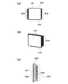
図1は、本発明の撮像装置の実施形態の一例であるデジタルビデオカメラの外観斜視図である。ここで、図1において、z軸は、カメラ本体102の前後方向を示し、紙面手前側を前端側、紙面奥側を後端側と定義する。また、このz軸は、カメラ本体102の撮像光軸に相当し、y軸は、カメラ本体102の上下方向に相当し、x軸は、カメラ本体102の左右方向に相当し、カメラ本体102を前端側から見てx軸方向の右側の側面を右側面とし、左側の側面を左側面とする。   FIG. 1 is an external perspective view of a digital video camera which is an example of an embodiment of an imaging apparatus of the present invention. Here, in FIG. 1, the z-axis indicates the front-rear direction of the camera body 102, and the front side of the page is defined as the front end side and the back side of the page is defined as the rear end side. The z axis corresponds to the imaging optical axis of the camera body 102, the y axis corresponds to the up and down direction of the camera body 102, the x axis corresponds to the left and right direction of the camera body 102, and the camera body 102 The right side surface in the x-axis direction when viewed from the front end side is the right side surface, and the left side surface is the left side surface.

図1に示すように、本実施形態のデジタルビデオカメラ101は、カメラ本体102を備え、カメラ本体102の前端側に形成された開口の内部には、レンズ鏡筒109が配置される。また、カメラ本体102の右側面には、2軸ヒンジ部114を介して表示ユニット103が開閉方向に回動可能、かつ開状態で回転可能に支持されている。カメラ本体102を右側面の後側には、メモリカード装着口110が設けられている。   As shown in FIG. 1, the digital video camera 101 of the present embodiment includes a camera body 102, and a lens barrel 109 is disposed inside an opening formed on the front end side of the camera body 102. The display unit 103 is supported on the right side surface of the camera body 102 via a biaxial hinge 114 so as to be rotatable in the opening / closing direction and rotatable in the open state. A memory card insertion slot 110 is provided on the rear side of the right side of the camera body 102.

図2(a)はレンズ鏡筒109をカメラ本体102の前端側から見た図、図2(b)は図2(a)の右側面図である。図3(a)は図2(a)のA−A線断面図、図3(b)は図2(b)のB−B線断面図である。   2A is a view of the lens barrel 109 viewed from the front end side of the camera body 102, and FIG. 2B is a right side view of FIG. 2A. 3A is a sectional view taken along line AA in FIG. 2A, and FIG. 3B is a sectional view taken along line BB in FIG. 2B.

レンズ鏡筒109は、本実施形態では、インナーフォーカス方式のレンズ鏡筒を採用しており、被写体側から像面側に向けて光軸に沿って1群レンズ401、2群レンズ402、防振レンズ403、及びアフォーカルレンズ404が配置されている。アフォーカルレンズ404の後方には、レンズ光学系を通過した光学像を電気信号に変換する撮像素子パッケージ201が配置されている。そして、1群レンズ401及び撮像素子パッケージ201の位置は固定され、2群レンズ402及びアフォーカルレンズ404が光軸方向に移動することでズーム動作及び合焦動作を行う。   In this embodiment, the lens barrel 109 employs an inner focus type lens barrel, and the first lens group 401, the second lens group 402, and the image stabilizers along the optical axis from the subject side toward the image plane side. A lens 403 and an afocal lens 404 are disposed. An image sensor package 201 that converts an optical image that has passed through the lens optical system into an electrical signal is disposed behind the afocal lens 404. The positions of the first group lens 401 and the image pickup device package 201 are fixed, and the second group lens 402 and the afocal lens 404 move in the optical axis direction to perform a zoom operation and a focusing operation.

具体的には、1群レンズ401は、固定鏡筒301に固定され、2群レンズ402は、第2鏡筒302に保持されて光軸方向に移動可能とされ、第2鏡筒302の後方側には、絞りユニット405が配置されている。絞りユニット405の後方側には、防振レンズ403が防振アクチュエータによって光軸と直交する方向に移動可能に保持され、防振レンズ403の後方側には、アフォーカルレンズ404が配置されている。アフォーカルレンズ404は、第3鏡筒303の内部で光軸方向に移動可能に設けられ、また、第3鏡筒303には、撮像素子パッケージ201が接着固定されたセンサープレート406が取り付けられる。   Specifically, the first lens group 401 is fixed to the fixed lens barrel 301, and the second lens group 402 is held by the second lens barrel 302 so as to be movable in the optical axis direction. A diaphragm unit 405 is arranged on the side. An anti-vibration lens 403 is held behind the aperture unit 405 so as to be movable in a direction perpendicular to the optical axis by an anti-vibration actuator, and an afocal lens 404 is arranged behind the anti-vibration lens 403. . The afocal lens 404 is provided so as to be movable in the direction of the optical axis inside the third lens barrel 303, and a sensor plate 406 to which the imaging element package 201 is bonded and fixed is attached to the third lens barrel 303.

1群レンズ401は、図3に示すように、後方に向けて縮径され、また、固定鏡筒301のカメラ本体102の右側面の側に位置する右側壁には、y軸に平行な軸を中心とする円弧状の切り欠き部407が形成されている。   As shown in FIG. 3, the first lens group 401 is reduced in diameter toward the rear, and the right wall located on the right side surface of the camera body 102 of the fixed barrel 301 has an axis parallel to the y axis. An arc-shaped notch 407 is formed with the center at the center.

また、第2鏡筒302のカメラ本体102の右側面の側に位置する右側壁は、固定鏡筒301の切り欠き部407が形成された右側壁に光軸方向に接しており、第2鏡筒302の右側壁の内面には、反射防止用の遮光形状部408が形成されている。本実施形態では、第2鏡筒302の右側壁を光軸に近づけることにより、カメラ本体102の小型化を可能にしている。また、第2鏡筒302の右側壁を光軸に近づけることにより、レンズ鏡筒109の内面での不要光の反射によるフレアやゴーストが起きやすくなるが、遮光形状部408により、反射光を遮断してフレアやゴーストを低減している。   The right side wall of the second lens barrel 302 located on the right side surface of the camera body 102 is in contact with the right side wall of the fixed lens barrel 301 where the notch 407 is formed in the optical axis direction. A light blocking shape portion 408 for preventing reflection is formed on the inner surface of the right side wall of the tube 302. In the present embodiment, the camera body 102 can be reduced in size by bringing the right side wall of the second lens barrel 302 closer to the optical axis. Further, by bringing the right side wall of the second lens barrel 302 closer to the optical axis, flare and ghost are likely to occur due to reflection of unnecessary light on the inner surface of the lens barrel 109, but the light shielding shape portion 408 blocks the reflected light. To reduce flare and ghosting.

第3鏡筒303は、光軸方向の前方がアフォーカルレンズ404の移動領域とされ、後方が撮像素子パッケージ201の取り付け領域413とされている。取り付け領域413には、赤外吸収ガラス409の収納部410、撮像素子パッケージ201の収納部411、センサープレート406の取り付け部が設けられる。   The third lens barrel 303 has a front area in the optical axis direction as a movement area of the afocal lens 404 and a rear area as an attachment area 413 of the imaging element package 201. The attachment area 413 is provided with a storage portion 410 for the infrared absorbing glass 409, a storage portion 411 for the image sensor package 201, and a mounting portion for the sensor plate 406.

図4(a)は撮像素子パッケージ201の正面図、図4(b)は撮像素子パッケージ201の斜視図、図4(c)は撮像素子パッケージ201の断面図である。図5(a)はセンサープレート406の正面図、図5(b)はセンサープレート406の斜視図である。   4A is a front view of the image sensor package 201, FIG. 4B is a perspective view of the image sensor package 201, and FIG. 4C is a cross-sectional view of the image sensor package 201. FIG. 5A is a front view of the sensor plate 406, and FIG. 5B is a perspective view of the sensor plate 406.

図4に示すように、撮像素子パッケージ201は、保護ガラス501、ベース部材502、リード503、及び撮像素子504を備える。ベース部材502には、撮像素子504が搭載される。撮像素子パッケージ201の裏面側には、センサープレート406が取り付けられる取り付け面505が形成されている。   As illustrated in FIG. 4, the imaging element package 201 includes a protective glass 501, a base member 502, leads 503, and an imaging element 504. An imaging element 504 is mounted on the base member 502. An attachment surface 505 to which the sensor plate 406 is attached is formed on the back side of the image sensor package 201.

図5に示すように、センサープレート406は、撮像素子パッケージ201が取り付けられる取り付け面506と、光軸方向の後方側に段差を有する複数(図では2つ)の当接面507とを有する。   As shown in FIG. 5, the sensor plate 406 includes an attachment surface 506 to which the image sensor package 201 is attached, and a plurality (two in the drawing) contact surfaces 507 having steps on the rear side in the optical axis direction.

また、当接面507と取り付け面506との間には、2つの段差接続部510a,510bが形成されている。センサープレート406の取り付け面506には、接着剤充填穴508、位置決め穴511、及び回転止め穴512が形成され、当接面507には、ビス挿通穴513が形成され、段差接続部510a,510bの間には、変形防止穴509が形成されている。2つの当接面507にそれぞれ形成されたビス挿通穴513は、撮像素子パッケージ201の中心に対して互いに略同一距離で対向配置されている。   In addition, two step connection portions 510 a and 510 b are formed between the contact surface 507 and the attachment surface 506. An attachment surface 506 of the sensor plate 406 is formed with an adhesive filling hole 508, a positioning hole 511, and a rotation stop hole 512, and a screw insertion hole 513 is formed on the contact surface 507, and the step connection portions 510a and 510b. Between them, a deformation preventing hole 509 is formed. Screw insertion holes 513 formed in the two contact surfaces 507 are opposed to each other at substantially the same distance from the center of the image pickup device package 201.

図6(a)はセンサープレート406に撮像素子パッケージ201を接着した状態の正面図、図6(b)は図6(a)の斜視図、図6(c)は図6(a)を裏面側から見た図である。図7(a)は、撮像素子パッケージ201を接着したセンサープレート406をレンズ鏡筒109の第3鏡筒303にビス止めにより取り付けた状態を示す斜視図である。図7(b)は、撮像素子パッケージ201を接着したセンサープレート406とレンズ鏡筒109の第3鏡筒303との取り付け部分の要部断面図である。   6A is a front view showing a state in which the image sensor package 201 is bonded to the sensor plate 406, FIG. 6B is a perspective view of FIG. 6A, and FIG. 6C is a back view of FIG. It is the figure seen from the side. FIG. 7A is a perspective view showing a state in which the sensor plate 406 to which the image pickup device package 201 is bonded is attached to the third lens barrel 303 of the lens barrel 109 with screws. FIG. 7B is a cross-sectional view of a main part of a mounting portion between the sensor plate 406 to which the image sensor package 201 is bonded and the third lens barrel 303 of the lens barrel 109.

センサープレート406は、撮像素子パッケージ201を第3鏡筒303に位置決め固定する部材である。センサープレート406の位置決め穴511を基準に、撮像素子パッケージ201を位置合わせして、撮像素子パッケージ201とセンサープレート406とを接着する。すなわち、撮像素子パッケージ201の取り付け面505とセンサープレート406の取り付け面506とを接触させた状態で、接着剤充填穴508に接着剤を充填することで、撮像素子パッケージ201とセンサープレート406とを接着する。   The sensor plate 406 is a member that positions and fixes the imaging element package 201 to the third lens barrel 303. The image sensor package 201 is aligned with the positioning hole 511 of the sensor plate 406 as a reference, and the image sensor package 201 and the sensor plate 406 are bonded. That is, with the mounting surface 505 of the imaging device package 201 and the mounting surface 506 of the sensor plate 406 in contact with each other, the adhesive filling hole 508 is filled with an adhesive so that the imaging device package 201 and the sensor plate 406 are connected. Glue.

そして、位置決め穴511及び回転止め穴512をそれぞれ第3鏡筒303の位置決めボス601及び回転止めボス602に嵌め込み、ビス挿通穴513から挿入したタップビス603を第3鏡筒303にねじ込む。これにより、センサープレート406が第3鏡筒303に取り付けられる。レンズ鏡筒109の光軸と撮像素子パッケージ201の撮像面の光軸方向の位置決めは、センサープレート406の取り付け面506のうち、撮像素子パッケージ201が取付けられることなく露出した領域を第3鏡筒303の当接面604に当接させることで行う。   Then, the positioning hole 511 and the rotation stop hole 512 are fitted into the positioning boss 601 and the rotation stop boss 602 of the third lens barrel 303, respectively, and the tap screw 603 inserted from the screw insertion hole 513 is screwed into the third lens barrel 303. As a result, the sensor plate 406 is attached to the third lens barrel 303. The positioning of the optical axis of the lens barrel 109 and the imaging surface of the imaging device package 201 in the optical axis direction is based on the third lens barrel in the mounting surface 506 of the sensor plate 406 where the imaging device package 201 is not attached. This is performed by contacting the contact surface 604 of 303.

ところで、センサープレート406の当接面507については、取り付け面506との間に段差を有しているため、取り付け面506と当接面507の両方を初期状態(ビス止め前の状態)で第3鏡筒303に当接させることは、部品の量産加工精度上困難である。   By the way, since the contact surface 507 of the sensor plate 406 has a step between it and the attachment surface 506, both the attachment surface 506 and the contact surface 507 are in the initial state (state before screwing). It is difficult to abut the three lens barrels 303 on the mass production processing accuracy of parts.

また、当接面507のみが第3鏡筒303に当接する寸法関係だと、第3鏡筒303の当接面604とセンサープレート406の取り付け面506との間に隙間が生じる。このため、レンズ鏡筒109の光軸と撮像素子パッケージ201の撮像面の光軸方向の距離関係に影響が生じる。   In addition, when only the contact surface 507 is in a dimensional relationship in which the third lens barrel 303 is in contact, a gap is generated between the contact surface 604 of the third lens barrel 303 and the mounting surface 506 of the sensor plate 406. This affects the distance relationship between the optical axis of the lens barrel 109 and the imaging surface of the imaging device package 201 in the optical axis direction.

本実施形態では、必ず第3鏡筒303の当接面604とセンサープレート406の取り付け面506とを当接させる。このため、センサープレート406の当接面507と第3鏡筒303のビス穴形成面605との隙間寸法S(図7(b))がS≧0となる寸法公差としている。   In the present embodiment, the contact surface 604 of the third lens barrel 303 and the mounting surface 506 of the sensor plate 406 are always brought into contact with each other. For this reason, the clearance dimension S (FIG. 7B) between the contact surface 507 of the sensor plate 406 and the screw hole forming surface 605 of the third lens barrel 303 is a dimensional tolerance that satisfies S ≧ 0.

これにより、センサープレート406を第3鏡筒303にビス止めしてセンサープレート406のビス挿通穴513の部分が第3鏡筒303に食い込んでも、光学系の移動量に影響を与えないようにすることができる。このため、センサープレート406のビス挿通穴513を光軸zに近づけて配置することができ、撮像素子パッケージ201の取り付け構造の小型化が可能となる。   Thus, even if the sensor plate 406 is screwed to the third lens barrel 303 and the screw insertion hole 513 portion of the sensor plate 406 bites into the third lens barrel 303, the movement amount of the optical system is not affected. be able to. For this reason, the screw insertion hole 513 of the sensor plate 406 can be disposed close to the optical axis z, and the mounting structure of the image sensor package 201 can be reduced in size.

一方、S>0の寸法交差でセンサープレート406を第3鏡筒303にタップビス603を介して取り付けると、センサープレート406の当接面507が変形し、その変形が接着剤充填穴508に及ぶと、接着強度が低下して剥離するおそれがある。   On the other hand, when the sensor plate 406 is attached to the third lens barrel 303 via the tap screw 603 at a dimension crossing of S> 0, the contact surface 507 of the sensor plate 406 is deformed, and the deformation reaches the adhesive filling hole 508. , There is a risk that the adhesive strength is lowered and peels off.

そこで、前述したように、センサープレート406の2つの段差接続部510a,510bの間に、変形防止穴509を形成して、段差接続部510a,510bを接着剤充填穴508から離れた位置に配置している。接着剤充填穴508は、図6(c)を参照して、段差接続部510a,510bに近い側514を遠い側515より大きな曲率半径の円弧形状としている。これにより、接着剤充填面積を確保しつつ段差接続部510,510bの変形を接着剤充填穴508に伝えないようにすることが可能である。   Therefore, as described above, the deformation prevention hole 509 is formed between the two step connection portions 510a and 510b of the sensor plate 406, and the step connection portions 510a and 510b are arranged at positions away from the adhesive filling hole 508. doing. With reference to FIG. 6C, the adhesive filling hole 508 has a side 514 close to the step connection portions 510 a and 510 b having an arc shape with a larger radius of curvature than the far side 515. Accordingly, it is possible to prevent the deformation of the step connection portions 510 and 510b from being transmitted to the adhesive filling hole 508 while securing the adhesive filling area.

つまり、接着剤充填穴508は、段差接続部510a,510bに近い側514と撮像素子パッケージ201の中心(光軸z)との距離L1が遠い側515と撮像素子パッケージ201の中心との距離L2よりも短いことになる。   That is, the adhesive filling hole 508 is a distance L2 between the side 515 far from the side 514 near the step connection portions 510a and 510b and the center (optical axis z) of the image sensor package 201 and the center of the image sensor package 201. Will be shorter.

また、段差接続部510aは、x軸方向に沿って形成され、段差接続部510bは、y軸方向に沿って形成されて、2つの段差接続部510a,510bの間に変形防止穴509が形成されている。さらに、変形防止穴509は、段差接続部510aがビス挿通穴513の中心からy軸方向に光軸z側に離れた位置に配置され、段差接続部510bがビス挿通穴513の中心からx軸方向に光軸z側に離れた位置に配置されるように形成されている。ここで、段差接続部510aは、本発明の第1の段差接続部の一例に相当し、段差接続部510bは、本発明の第2の段差接続部の一例に相当する。   Further, the step connection portion 510a is formed along the x-axis direction, and the step connection portion 510b is formed along the y-axis direction, and a deformation prevention hole 509 is formed between the two step connection portions 510a and 510b. Has been. Further, the deformation preventing hole 509 is disposed at a position where the step connection portion 510a is separated from the center of the screw insertion hole 513 in the y-axis direction toward the optical axis z, and the step connection portion 510b is disposed from the center of the screw insertion hole 513 to the x axis. It is formed so as to be disposed at a position away from the optical axis z in the direction. Here, the step connection portion 510a corresponds to an example of the first step connection portion of the present invention, and the step connection portion 510b corresponds to an example of the second step connection portion of the present invention.

このように、2つの段差接続部510a,510bが光軸zに直交するx軸方向及びy軸方向の2方向に形成されることで、段差接続部510a,510bがx軸回り及びy軸回りに回転変形する要素を抑制し合うことになる。これにより、ビス挿通穴513に挿通したタップビス603をビス穴形成面605にねじ込むことで、当接面507がビス穴形成面605に対して変形する際、当接面507を光軸zに沿って平行移動しやすくすることが可能となる。   As described above, the two step connection portions 510a and 510b are formed in the two directions of the x-axis direction and the y-axis direction orthogonal to the optical axis z, so that the step connection portions 510a and 510b are about the x-axis and the y-axis. Therefore, the elements that are rotationally deformed are suppressed. Thus, when the contact surface 507 is deformed with respect to the screw hole forming surface 605 by screwing the tap screw 603 inserted into the screw insertion hole 513 into the screw hole forming surface 605, the contact surface 507 is moved along the optical axis z. It is possible to facilitate parallel movement.

図8(a)はセンサープレート406に貼り付けられた撮像素子パッケージ201を素子基板202に実装した状態を示す斜視図、図8(b)は図8(a)を背面側から見た斜視図である。図8(c)は、素子基板202をメイン基板204に接続した状態を示す斜視図である。   8A is a perspective view showing a state where the image pickup device package 201 attached to the sensor plate 406 is mounted on the element substrate 202, and FIG. 8B is a perspective view of FIG. 8A viewed from the back side. It is. FIG. 8C is a perspective view showing a state where the element substrate 202 is connected to the main substrate 204.

素子基板202には、撮像素子パッケージ201で光電変換された信号をデジタル信号に変換するAD変換IC203及び周辺回路が実装され、AD変換IC203は、撮像素子パッケージ201の実装面の反対側の面に実装されている。素子基板202のAD変換IC203でAD変換された映像信号は、コネクタ実装部701に実装されたBtoBコネクタ702を介してメイン基板204に出力される。   The element substrate 202 is mounted with an AD conversion IC 203 and a peripheral circuit that convert a signal photoelectrically converted by the imaging element package 201 into a digital signal. The AD conversion IC 203 is mounted on a surface opposite to the mounting surface of the imaging element package 201. Has been implemented. The video signal AD-converted by the AD conversion IC 203 of the element substrate 202 is output to the main substrate 204 via the BtoB connector 702 mounted on the connector mounting portion 701.

図9(a)は、素子基板202に放熱板703をビス止めにより取り付けた状態を撮像素子パッケージ201の裏面側から見た斜視図である。   FIG. 9A is a perspective view of the state in which the heat radiating plate 703 is attached to the element substrate 202 with screws, as viewed from the back side of the imaging element package 201.

放熱板703は、素子基板202と平行な主面部704と、主面部704からz軸方向を後方に延びる放熱腕705と、主面部704からz軸方向を前方に延びる放熱腕706とを有する。放熱腕705は、カメラ本体102の右側面の側に配置され、放熱腕706、カメラ本体102の左側面の側に配置される。   The heat radiating plate 703 includes a main surface portion 704 parallel to the element substrate 202, a heat radiating arm 705 extending rearward from the main surface portion 704 in the z-axis direction, and a heat radiating arm 706 extending forward from the main surface portion 704 in the z-axis direction. The heat dissipating arm 705 is disposed on the right side of the camera body 102, and is disposed on the left side of the heat dissipating arm 706 and the camera body 102.

また、主面部704のAD変換IC203と対向する位置には、絞り部708が形成され、これにより、放熱板703をAD変換IC203に近づけることが可能になり、AD変換IC203の放熱を効率よく行うことができる。   In addition, a diaphragm portion 708 is formed at a position facing the AD conversion IC 203 on the main surface portion 704, which makes it possible to bring the heat radiating plate 703 closer to the AD conversion IC 203, thereby efficiently radiating heat from the AD conversion IC 203. be able to.

図9(b)は、放熱板703の放熱腕705,706にそれぞれ弾性導電放熱部材707を取り付けた状態を撮像素子パッケージ201側から見た斜視図である。弾性導電放熱部材707は、周囲の構造部材に弾性的に接触して素子基板202や撮像素子パッケージ201等で発生した電気ノイズの導電や熱の放散を行う。   FIG. 9B is a perspective view of the state where the elastic conductive heat radiating member 707 is attached to the heat radiating arms 705 and 706 of the heat radiating plate 703 as viewed from the image pickup device package 201 side. The elastic conductive heat radiating member 707 elastically contacts with surrounding structural members and conducts electrical noise generated in the element substrate 202, the image pickup element package 201, and the like and dissipates heat.

図10(a)は弾性導電放熱部材707の模式図、図10(b)は放熱板703の放熱腕705,706と弾性導電放熱部材707と周囲の構造部材805との関係を示す模式図である。   FIG. 10A is a schematic diagram of the elastic conductive heat dissipation member 707, and FIG. 10B is a schematic diagram illustrating the relationship among the heat dissipation arms 705 and 706 of the heat dissipation plate 703, the elastic conductive heat dissipation member 707, and the surrounding structural member 805. is there.

弾性導電放熱部材707は、プラスチックシート801に銅箔やアルミ箔等の金属箔802を貼り付けたシートを、金属箔802が外側を向くように折り曲げ、内側に両面テープ803を貼り付けた発泡ウレタンやスポンジ等の弾性部材804を挟んで形成される。なお、プラスチックシート801は、厚さ0.05〜0.3mm程度のものが用いられ、金属箔802は、厚さ0.05〜0.5mm程度のものが用いられる。   The elastic conductive heat radiating member 707 is a urethane foam in which a sheet of metal foil 802 such as copper foil or aluminum foil is attached to a plastic sheet 801, bent so that the metal foil 802 faces outward, and a double-sided tape 803 is attached inside. And an elastic member 804 such as a sponge. The plastic sheet 801 has a thickness of about 0.05 to 0.3 mm, and the metal foil 802 has a thickness of about 0.05 to 0.5 mm.

両面テープ803は、金属箔802及びプラスチックシート801に対して一部が露出するように貼り付けられ、この露出部分を用いて放熱板703の放熱腕705,706に貼り付けを行う。   The double-sided tape 803 is attached to the metal foil 802 and the plastic sheet 801 so as to be partially exposed, and is attached to the heat dissipation arms 705 and 706 of the heat dissipation plate 703 using the exposed portions.

図10(b)に示すように、弾性導電放熱部材707は、放熱板703の放熱腕705,706と対向する面の構造部材805にも金属箔802が対向し、金属箔802は、弾性部材804によって構造部材805に押し付けられて導電及び放熱を行う。また、弾性導電放熱部材707は、略U字形状を有しており、U字部分806が熱源である撮像素子パッケージ201や素子基板202に近い放熱板703の主面部704側になるように配置することで、放熱効果を高めることが可能である。   As shown in FIG. 10B, the elastic conductive heat radiation member 707 has a metal foil 802 opposed to a structural member 805 on the surface of the heat radiation plate 703 facing the heat radiation arms 705 and 706, and the metal foil 802 is made of an elastic member. It is pressed against the structural member 805 by 804 to conduct and dissipate heat. The elastic conductive heat radiating member 707 has a substantially U shape, and is arranged so that the U-shaped portion 806 is on the main surface portion 704 side of the heat radiating plate 703 close to the imaging element package 201 and the element substrate 202 which are heat sources. By doing so, it is possible to enhance the heat dissipation effect.

また、金属箔802の支持材としてプラスチックシート801を用いることにより、金属箔802の塑性変形を防止して弾性部材804の反発力を妨げないようにすることができる。このように構成することによって、導電かつ放熱を1つの部材で行うことが可能となり、放熱ゴムやガスケットを併用せず、低コスト化及び省スペース化を図ることが可能となる。なお、本実施形態では、1枚の両面テープを用いているが、弾性部材804を挟んで2枚の両面テープを用いたり、1枚の長い両面テープで弾性部材804を包むなどしてもよい。   In addition, by using the plastic sheet 801 as a support material for the metal foil 802, plastic deformation of the metal foil 802 can be prevented so that the repulsive force of the elastic member 804 is not hindered. With this configuration, it is possible to conduct and dissipate heat with a single member, and it is possible to reduce costs and save space without using a heat radiating rubber or gasket. In this embodiment, one double-sided tape is used, but two double-sided tapes may be used with the elastic member 804 interposed therebetween, or the elastic member 804 may be wrapped with one long double-sided tape. .

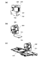
次に、図11(a)及び図11(b)を参照して、カメラ本体102の右側面の外装カバーとレンズ鏡筒109との間に配置される右側板金部材901について説明する。図11(a)は右側板金部材901の外観斜視図、図11(b)は右側板金部材901の上方から見た平面図である。   Next, with reference to FIG. 11A and FIG. 11B, the right sheet metal member 901 disposed between the outer cover on the right side of the camera body 102 and the lens barrel 109 will be described. 11A is an external perspective view of the right sheet metal member 901, and FIG. 11B is a plan view of the right sheet metal member 901 viewed from above.

右側板金部材901は、熱伝導性の高いアルミ合金や銅合金等で形成され、右側面を形成する主面部902、前後方向(z軸方向)に互いに離間して配置された2カ所の上面部903,604及び下面部905により略コ字形状をなしている。   The right sheet metal member 901 is formed of an aluminum alloy, a copper alloy, or the like with high thermal conductivity, and a main surface portion 902 that forms the right side surface, and two upper surface portions that are spaced apart from each other in the front-rear direction (z-axis direction). 903 and 604 and the lower surface part 905 form a substantially U shape.

上面部903の後側には、図11(b)に示すように、上方から平面視してz軸に対して約65°の角度θで斜めに交差して配置される曲げ部906が設けられ、下面部905の後側には、スリット907が曲げ部906と対向して斜めに延びて形成されている。右側板金部材901の主面部902には、2か所の穴部908が前後方向に互いに離間して形成され、穴部908には、レンズ受け弾性部材1001(図12参照)が装着される。   On the rear side of the upper surface portion 903, as shown in FIG. 11B, there is provided a bending portion 906 that is arranged obliquely intersecting at an angle θ of about 65 ° with respect to the z axis in plan view from above. On the rear side of the lower surface portion 905, a slit 907 is formed so as to extend obliquely facing the bent portion 906. Two holes 908 are formed in the main surface portion 902 of the right sheet metal member 901 so as to be separated from each other in the front-rear direction, and a lens receiving elastic member 1001 (see FIG. 12) is attached to the hole 908.

次に、図11(c)を参照して、カメラ本体102の左側面の外装カバーとレンズ鏡筒109との間に配置される左側板金部材909について説明する。図11(c)は、左側板金部材909の外観斜視図である。   Next, with reference to FIG. 11C, the left sheet metal member 909 disposed between the exterior cover on the left side of the camera body 102 and the lens barrel 109 will be described. FIG. 11C is an external perspective view of the left sheet metal member 909.

左側板金部材909は、熱伝導性の高いアルミ合金や銅合金等で形成され、左側面を形成する主面部910、前後方向(z軸方向)に互いに離間して配置された2カ所の上面部911,912及び下面部913により略コ字形状をなしている。下面部913の後側には、右側板金部材901のスリット907と同方向に延びるスリット914が形成されている。左側板金部材909の主面部910には、1か所の穴部915が形成され、穴部915には、レンズ受け弾性部材1001が装着される。   The left sheet metal member 909 is made of a highly heat conductive aluminum alloy, copper alloy, or the like, a main surface portion 910 that forms the left side surface, and two upper surface portions that are spaced apart from each other in the front-rear direction (z-axis direction) 911 and 912 and the lower surface portion 913 form a substantially U shape. A slit 914 extending in the same direction as the slit 907 of the right sheet metal member 901 is formed on the rear side of the lower surface portion 913. One hole 915 is formed in the main surface 910 of the left sheet metal member 909, and the lens receiving elastic member 1001 is mounted in the hole 915.

図12(a)はレンズ受け弾性部材1001の側面図、図12(b)はレンズ受け弾性部材1001の斜視図である。   12A is a side view of the lens receiving elastic member 1001, and FIG. 12B is a perspective view of the lens receiving elastic member 1001. FIG.

レンズ受け弾性部材1001は、軸方向に同軸に並んで形成された大径部1002、小径部1003及び中径部1004を有し、中心部には、穴1005が貫通して形成されている。大径部1002、及び中径部1004の外端外周部、並びに穴1005の両端内周部には、面取り1006が施されている。   The lens receiving elastic member 1001 has a large-diameter portion 1002, a small-diameter portion 1003, and a medium-diameter portion 1004 that are formed coaxially in the axial direction, and a hole 1005 is formed through the center portion. Chamfering 1006 is applied to the outer peripheral portions of the large-diameter portion 1002 and the medium-diameter portion 1004 and the inner peripheral portions of both ends of the hole 1005.

図13(a)は右側板金部材901の2か所の穴部908にレンズ受け弾性部材1001を装着した状態の外観斜視図、図13(b)は左側板金部材909の穴部915にレンズ受け弾性部材1001を装着した状態の外観斜視図である。   13A is an external perspective view showing a state in which the lens receiving elastic member 1001 is mounted in the two holes 908 of the right sheet metal member 901, and FIG. 13B is a lens receiving in the hole 915 of the left sheet metal member 909. FIG. 3 is an external perspective view of a state where an elastic member 1001 is mounted.

右側板金部材901の穴部908には、接触面積の大きな大径部1002がレンズ鏡筒109側に配置されるように小径部1003が嵌め込まれて、右側板金部材901が大径部1002と中径部1004との間に挟まれた状態となる。左側板金部材909も同様に、接触面積の大きな大径部1002がレンズ鏡筒109側に配置されるように穴部915に小径部1003が嵌め込まれて、左側板金部材909が大径部1002と中径部1004との間に挟まれた状態となる。   The small-diameter portion 1003 is fitted in the hole 908 of the right-side sheet metal member 901 so that the large-diameter portion 1002 having a large contact area is disposed on the lens barrel 109 side. It is in a state of being sandwiched between the diameter portion 1004. Similarly, the left-side sheet metal member 909 is fitted with the small-diameter portion 1003 in the hole 915 so that the large-diameter portion 1002 having a large contact area is disposed on the lens barrel 109 side. It is in a state of being sandwiched between the middle diameter portion 1004.

図14(a)は、右側板金部材901の曲げ部906、スリット907、及び左側板金部材のスリット914にカード基板1101を取り付ける様子を示す斜視図である。図14(b)は右側板金部材901の曲げ部906、スリット907、及び左側板金部材のスリット914にカード基板1101を取り付けた状態を示す斜視図、図14(c)は図14(b)を上方から見た平面図である。   FIG. 14A is a perspective view showing a state in which the card substrate 1101 is attached to the bent portion 906 of the right side sheet metal member 901, the slit 907, and the slit 914 of the left side sheet metal member. FIG. 14B is a perspective view showing a state in which the card substrate 1101 is attached to the bent portion 906, the slit 907, and the slit 914 of the left sheet metal member 901, and FIG. 14C shows FIG. 14B. It is the top view seen from the upper part.

カード基板1101には、外部メモリカードが接続されるカードスロット1102が実装される。そして、図14(a)に示すように、カード基板1101に設けられた差し込み部1107をスリット907とスリット914に挿入した後、曲げ部906にカード基板1101を押し当てて不図示のビスによって締結する。   A card slot 1102 to which an external memory card is connected is mounted on the card substrate 1101. 14A, after inserting the insertion portion 1107 provided on the card substrate 1101 into the slit 907 and the slit 914, the card substrate 1101 is pressed against the bending portion 906 and fastened with a screw (not shown). To do.

ここで、前述したように、曲げ部906及び2か所のスリット907,914がレンズ鏡筒109の光軸zに対して約65°傾いているため、カード基板1101も光軸zに対して傾いて取り付けられる。   Here, as described above, since the bent portion 906 and the two slits 907 and 914 are inclined by about 65 ° with respect to the optical axis z of the lens barrel 109, the card substrate 1101 also has the optical axis z. Mounted at an angle.

右側板金部材901及び左側板金部材909は、前述したように、それぞれ略コ字状に形成されているため、右側板金部材901及び左側板金部材909を組み合わせた構造体は、断面矩形状となり、平行四辺形状の変形に対して強度的に問題がある。しかし、カード基板1101を斜めに傾けて取り付けることによって、カード基板1101が筋交いとして補強部材の役割を担うことができる。   Since the right sheet metal member 901 and the left sheet metal member 909 are each formed in a substantially U shape as described above, the structure in which the right sheet metal member 901 and the left sheet metal member 909 are combined has a rectangular cross section and is parallel to each other. There is a problem in strength against the deformation of the quadrilateral shape. However, by attaching the card substrate 1101 obliquely, the card substrate 1101 can serve as a reinforcing member as a brace.

また、カード基板1101の傾斜角度θ=約65°は、光軸z方向から見たカード基板1101の投影面積が、レンズ鏡筒109の投影面積にほぼ収まるように決定される。つまり、図14(c)に示すように、右側板金部材901と左側板金部材909による撮像レンズ収納幅B1が、カード基板1101の光軸z方向に占有する幅B2と略等しくなっている。   Further, the inclination angle θ of the card substrate 1101 = about 65 ° is determined so that the projected area of the card substrate 1101 viewed from the optical axis z direction is substantially within the projected area of the lens barrel 109. That is, as shown in FIG. 14C, the imaging lens storage width B1 by the right sheet metal member 901 and the left sheet metal member 909 is substantially equal to the width B2 occupied in the optical axis z direction of the card substrate 1101.

このように傾斜角度θを決定することにより、カメラ本体102の左右方向(x方向)の幅をレンズ鏡筒109の幅で決定される要素以上に大型化することなく、小型なカメラ本体102とすることができる。また、カード基板1101の上下方向(y軸方向)高さは、カード基板1101の左右方向(x軸方向)の幅B2よりも短く、レンズ鏡筒109の上下方向の高さに収まるようになっている。さらに、カード基板1101のカードスロット1102の実装面の反対側の面には、バックアップ用蓄電池1105が実装されている。   By determining the inclination angle θ in this way, the camera body 102 can be reduced in size without increasing the width of the camera body 102 in the left-right direction (x direction) beyond the element determined by the width of the lens barrel 109. can do. Also, the height of the card substrate 1101 in the vertical direction (y-axis direction) is shorter than the width B2 of the card substrate 1101 in the horizontal direction (x-axis direction), so that the height of the lens barrel 109 is within the vertical direction. ing. Further, a backup storage battery 1105 is mounted on the surface of the card board 1101 opposite to the mounting surface of the card slot 1102.

図15(a)は右側板金部材901及び左側板金部材909をレンズ鏡筒109に取り付けた状態を上面側から見た斜視図、図15(b)は右側板金部材901及び左側板金部材909をレンズ鏡筒109に取り付けた状態を下面側から見た斜視図である。   15A is a perspective view of the state in which the right sheet metal member 901 and the left sheet metal member 909 are attached to the lens barrel 109 as viewed from the upper surface side, and FIG. 15B shows the right sheet metal member 901 and the left sheet metal member 909 as lenses. It is the perspective view which looked at the state attached to the lens-barrel 109 from the lower surface side.

レンズ鏡筒109には、右側板金部材901及び左側板金部材909に装着されたレンズ受け弾性部材1001の穴1005に嵌合される軸部1202が形成されている。右側板金部材901の上面部903と左側板金部材909の上面部911は、不図示の掛止爪を介して接続され、右側板金部材901の上面部904と左側板金部材909の上面部912も、不図示の掛止爪を介して接続される。右側板金部材901の下面部905と左側板金部材909の下面部913とは、ビス1201によって締結される。   The lens barrel 109 is formed with a shaft portion 1202 that fits into the hole 1005 of the lens receiving elastic member 1001 attached to the right sheet metal member 901 and the left sheet metal member 909. The upper surface part 903 of the right sheet metal member 901 and the upper surface part 911 of the left sheet metal member 909 are connected via a not-shown latching claw, and the upper surface part 904 of the right sheet metal member 901 and the upper surface part 912 of the left sheet metal member 909 are also It is connected via a latching claw (not shown). The lower surface portion 905 of the right sheet metal member 901 and the lower surface portion 913 of the left sheet metal member 909 are fastened by screws 1201.

レンズ鏡筒109は、右側板金部材901及び左側板金部材909の組立構造体に対してレンズ受け弾性部材1001の弾性力のみによって保持されている。これにより、右側板金部材901と左側板金部材909に取り付けられる外装部材等からの負荷をレンズ鏡筒109に伝えにくくすることができ、また、レンズ鏡筒109で発する振動や騒音を外装部材等に伝えにくくすることができる。   The lens barrel 109 is held only by the elastic force of the lens receiving elastic member 1001 with respect to the assembly structure of the right sheet metal member 901 and the left sheet metal member 909. Thereby, it is possible to make it difficult to transmit the load from the exterior member attached to the right sheet metal member 901 and the left sheet metal member 909 to the lens barrel 109, and vibration and noise generated by the lens barrel 109 are transmitted to the exterior member and the like. It can be difficult to convey.

図16(a)はメイン基板204に三脚ねじ部材1301及び補強板金部材1302を組み付けた状態の斜視図、図16(b)は図16(a)の分解斜視図、図16(c)は図16(a)の下方から見た斜視図である。   16A is a perspective view of a state in which the tripod screw member 1301 and the reinforcing sheet metal member 1302 are assembled to the main board 204, FIG. 16B is an exploded perspective view of FIG. 16A, and FIG. It is the perspective view seen from the downward direction of 16 (a).

メイン基板204は、三脚ねじ部材1301との間に補強板金部材1302を挟んでユニット化された状態で右側板金部材901及び左側板金部材909の組立構造体の下面側に取り付けられる。メイン基板204には、前述した素子基板202がコネクタ接続されるとともに、レンズ鏡筒109の駆動アクチュエータ及び駆動系の位置検出手段等に接続されるFPC等が接続されている。また、メイン基板204の下面側には、HDMI端子1303、USB端子1304、及び電源入力端子112が実装されている。   The main board 204 is attached to the lower surface side of the assembly structure of the right sheet metal member 901 and the left sheet metal member 909 in a unit state with the reinforcing sheet metal member 1302 sandwiched between the main board 204 and the tripod screw member 1301. The main substrate 204 is connected to the element substrate 202 described above by a connector, and is connected to an FPC connected to a drive actuator of the lens barrel 109, a position detection unit of the drive system, and the like. An HDMI terminal 1303, a USB terminal 1304, and a power input terminal 112 are mounted on the lower surface side of the main board 204.

三脚ねじ部材1301は、繊維強化プラスチック等で形成されており、回転止め部1305、三脚ねじ部1306、補強板金部材1302の取り付け部1307、及び端子補強部1308を有する。   The tripod screw member 1301 is made of fiber reinforced plastic or the like, and includes a rotation stop portion 1305, a tripod screw portion 1306, a mounting portion 1307 of the reinforcing sheet metal member 1302, and a terminal reinforcing portion 1308.

三脚ねじ部1306には、三脚が締結されるねじが形成され、回転止め部1305には、三脚の回転止め凸部が嵌合する凹部が形成されている。三脚ねじ部1306の上面部は、三脚を取り付けた際に突き上げる力が加わるため、補強板金部材1302を取り付けて補強する。端子補強部1308は、HDMI端子1303、USB端子1304、電源入力端子112の基板側の反対面を支持して補強する。   The tripod screw portion 1306 is formed with a screw to which the tripod is fastened, and the rotation stop portion 1305 is formed with a recess into which the rotation stop projection portion of the tripod is fitted. The upper surface portion of the tripod screw portion 1306 is reinforced by attaching a reinforcing sheet metal member 1302 because a force to push up is applied when the tripod is attached. The terminal reinforcing portion 1308 supports and reinforces the opposite surfaces of the HDMI terminal 1303, the USB terminal 1304, and the power input terminal 112 on the board side.

図17は、図16に示すメイン基板ユニットの補強板金部材1302に、端子基板1309及びメモリ基板1310を取り付けた状態を示す斜視図である。   FIG. 17 is a perspective view showing a state in which the terminal board 1309 and the memory board 1310 are attached to the reinforcing sheet metal member 1302 of the main board unit shown in FIG.

図17に示すように、メイン基板ユニットの補強板金部材1302には、映像音声出力端子1311及び外部マイク入力端子1312を実装した端子基板1309、及び不図示の内蔵メモリを実装したメモリ基板1310がそれぞれ締結されてユニット化される。   As shown in FIG. 17, the reinforcing sheet metal member 1302 of the main board unit includes a terminal board 1309 on which an audio / video output terminal 1311 and an external microphone input terminal 1312 are mounted, and a memory board 1310 on which a built-in memory (not shown) is mounted. It is fastened and unitized.

図18(a)は、レンズ鏡筒109に右側板金部材901及び左側板金部材909を取り付けた図15に示すユニットに、図17に示すユニットとカード基板1101を取り付けた状態を示す斜視図である。図18(b)は、図18(a)の状態における素子基板202、メイン基板204、及びカード基板1101の位置関係を示す斜視図である。   FIG. 18A is a perspective view showing a state where the unit shown in FIG. 17 and the card substrate 1101 are attached to the unit shown in FIG. 15 in which the right sheet metal member 901 and the left sheet metal member 909 are attached to the lens barrel 109. . FIG. 18B is a perspective view showing a positional relationship among the element substrate 202, the main substrate 204, and the card substrate 1101 in the state of FIG.

カード基板1101の下部には、凸部1401が設けられ、凸部1401と対向する位置には、素子基板202のコネクタ実装部701に実装されたBtoBコネクタ702とメイン基板204との接続部が配置される。   A convex portion 1401 is provided at a lower portion of the card substrate 1101, and a connection portion between the BtoB connector 702 mounted on the connector mounting portion 701 of the element substrate 202 and the main substrate 204 is disposed at a position facing the convex portion 1401. Is done.

図18(c)は、図18(a)を上面側から見た平面図である。図18(c)に示すように、凸部1401は、カード基板1101とBtoBコネクタとの交差位置に配置されている。このように配置することにより、BtoBコネクタ702がその短辺および長辺を軸に回転するのを規制して接続不良を起こすのを防止することができる。また、凸部1401と素子基板202のコネクタ実装部701との距離を、BtoBコネクタ702の嵌合量を上回らないようにすることで、BtoBコネクタ702の不用意な抜けを防止することができる。   FIG.18 (c) is the top view which looked at Fig.18 (a) from the upper surface side. As shown in FIG. 18C, the convex portion 1401 is arranged at the intersection of the card substrate 1101 and the BtoB connector. By arranging in this way, it is possible to prevent the BtoB connector 702 from rotating around the short side and the long side as an axis, thereby preventing poor connection. Further, by preventing the distance between the convex portion 1401 and the connector mounting portion 701 of the element substrate 202 from exceeding the fitting amount of the BtoB connector 702, the BtoB connector 702 can be prevented from being unintentionally disconnected.

図19(a)は、図18(a)の状態におけるレンズ鏡筒109とカード基板1101と放熱板703との位置関係を示す上面図である。   FIG. 19A is a top view showing a positional relationship among the lens barrel 109, the card substrate 1101, and the heat radiating plate 703 in the state of FIG.

図19(a)に示すように、放熱板703の主面部704とカード基板1101とによって形成される三角形状のスペース1402(図の破線部)に、放熱板703の右側の放熱腕705が配置される。放熱腕705にヘミング加工を施すことで、三角形状のスペース1402を放熱スペースとして利用している。また、三角形状のスペース1402とカード基板1101を挟んで反対側のスペースには、バックアップ用蓄電池1105を配置して、スペースを有効利用している。   As shown in FIG. 19A, the right side heat dissipation arm 705 of the heat dissipation plate 703 is arranged in a triangular space 1402 (broken line portion in the figure) formed by the main surface portion 704 of the heat dissipation plate 703 and the card substrate 1101. Is done. By applying a hemming process to the heat dissipating arm 705, the triangular space 1402 is used as a heat dissipating space. Further, a backup storage battery 1105 is disposed in the space on the opposite side across the triangular space 1402 and the card substrate 1101 to effectively use the space.

図19(b)は、図18(a)に示す構造体に操作ユニット1403を取り付けた状態を示す斜視図である。   FIG. 19B is a perspective view showing a state in which the operation unit 1403 is attached to the structure shown in FIG.

操作ユニット1403は、ズームスイッチ1404を及び電源スイッチ1405及び録画スイッチ1406がユニット化されている。操作ユニット1403は、右側板金部材901と左側板金部材909が上面で締結された位置で、カード基板1101の上面部に取り付けられる。操作ユニット1403とメイン基板204とは、FPC1407で接続され、FPC1407は、分岐してカード基板1101のコネクタ1408に接続されて、カード基板1101とメイン基板204との接続も兼ねている。   The operation unit 1403 includes a zoom switch 1404, a power switch 1405, and a recording switch 1406 as a unit. The operation unit 1403 is attached to the upper surface portion of the card substrate 1101 at a position where the right sheet metal member 901 and the left sheet metal member 909 are fastened on the upper surface. The operation unit 1403 and the main board 204 are connected by an FPC 1407, and the FPC 1407 is branched and connected to the connector 1408 of the card board 1101, which also serves as a connection between the card board 1101 and the main board 204.

図20(a)は図19(b)に示す構造体にカメラ本体102の右側面カバー104及び表示ユニット103を取り付けた状態を示す斜視図、図20(b)はカメラ本体102の底面側のバッテリ周辺部を示す図である。図20(c)は、図20(a)を後側から見た図である。   20A is a perspective view showing a state where the right side cover 104 and the display unit 103 of the camera body 102 are attached to the structure shown in FIG. 19B, and FIG. 20B is a bottom view of the camera body 102. It is a figure which shows a battery peripheral part. FIG.20 (c) is the figure which looked at Fig.20 (a) from the rear side.

バッテリ213は、右側面カバー104の後側に設けられたバッテリ取り付け部108に取り付けられる。バッテリ取り付け部108をカメラ本体102の底面側から見たとき、バッテリ取り付け部108の最大左右幅H1の中心1503より取り付けレール幅H2の中心1504がカメラ本体102の左側面に接近して配置される。   The battery 213 is attached to a battery attachment portion 108 provided on the rear side of the right side cover 104. When the battery mounting portion 108 is viewed from the bottom side of the camera body 102, the center 1504 of the mounting rail width H2 is arranged closer to the left side surface of the camera body 102 than the center 1503 of the maximum left-right width H1 of the battery mounting portion 108. .

図21(a)はバッテリ213の斜視図、図21(b)はバッテリ213を取り付け面側から見た正面図、図21(c)は図21(b)のC−C線断面図である。   21A is a perspective view of the battery 213, FIG. 21B is a front view of the battery 213 viewed from the mounting surface side, and FIG. 21C is a cross-sectional view taken along the line CC in FIG. 21B. .

バッテリ213は、リチウムイオン電池のセル1601、回路基板1602及びコネクタ1603を、取り付け部カバー1604と外観カバー1605との間に挟んで構成される。取り付け部カバー1604の取り付け部の左右幅H3の中心1608は、取り付け部カバー1604の左右幅H4(=外観カバー1605の左右幅)の中心1609より取り付け面から見て左側に偏って配置されている。これに起因して、前述したように、バッテリ取り付け部108の最大左右幅H1の中心1503より取り付けレール幅H2の中心1504がカメラ本体102の左側面に接近して配置されている。   The battery 213 includes a lithium-ion battery cell 1601, a circuit board 1602, and a connector 1603 sandwiched between an attachment portion cover 1604 and an exterior cover 1605. The center 1608 of the left and right width H3 of the attachment portion of the attachment portion cover 1604 is arranged to be shifted to the left as viewed from the attachment surface from the center 1609 of the left and right width H4 of the attachment portion cover 1604 (= left and right width of the appearance cover 1605). . Due to this, as described above, the center 1504 of the mounting rail width H2 is arranged closer to the left side surface of the camera body 102 than the center 1503 of the maximum left-right width H1 of the battery mounting portion 108.

図21(c)に示すように、バッテリ213の内部においても、セル1601の中心1616に対して、回路基板1602の中心1617が左側に偏って配置されている。そして、セル1601と回路基板1602の偏りは左右方向だけではなく、図21(b)に示すように、上下方向にも偏りをもっている。つまり、取り付け部カバー1604の取り付け部の上下高さT1は、取り付け部カバー1604全体の上下高さT2(=外観カバー1605の上下高さ)より上面側に偏っており、段差T3が生じるようになっている。   As shown in FIG. 21 (c), the center 1617 of the circuit board 1602 is also arranged on the left side with respect to the center 1616 of the cell 1601 even inside the battery 213. The deviation between the cell 1601 and the circuit board 1602 is not only in the horizontal direction but also in the vertical direction as shown in FIG. That is, the vertical height T1 of the mounting portion of the mounting portion cover 1604 is biased to the upper surface side from the vertical height T2 of the entire mounting portion cover 1604 (= the vertical height of the appearance cover 1605) so that a step T3 is generated. It has become.

図22(a)は、本実施形態のデジタルビデオカメラ101よりバッテリ取り付け部が小さいタイプのデジタルビデオカメラ1613にバッテリ213を取り付けた状態の模式図である。図22(b)は、デジタルビデオカメラ1613をカメラ本体1614の右側面から見た模式図である。   FIG. 22A is a schematic diagram of a state in which a battery 213 is attached to a digital video camera 1613 of a type having a battery attachment portion smaller than that of the digital video camera 101 of the present embodiment. FIG. 22B is a schematic view of the digital video camera 1613 as viewed from the right side of the camera body 1614.

デジタルビデオカメラ1613は、カメラ本体1614の右側面に2軸ヒンジ部114を介して表示ユニット1615が開閉方向に回動可能、かつ開状態で回転可能に支持されている。カメラ本体1614の後側に設けられたバッテリ取り付け部108の左右幅H1は、バッテリ213側の取り付け部の左右幅H3(図21(b)参照)と略同じ幅とされている。このようなデジタルビデオカメラ1613のバッテリ取り付け部108にバッテリ213を取り付けると、表示ユニット1615は全閉状態にはならないものの、バッテリ213を取り付けて使用することは可能である。   In the digital video camera 1613, a display unit 1615 is supported on the right side surface of a camera body 1614 via a biaxial hinge portion 114 so as to be rotatable in an opening / closing direction and rotatable in an open state. The left-right width H1 of the battery attachment portion 108 provided on the rear side of the camera body 1614 is substantially the same as the left-right width H3 (see FIG. 21B) of the attachment portion on the battery 213 side. When the battery 213 is attached to the battery attachment portion 108 of the digital video camera 1613, the display unit 1615 is not fully closed, but the battery 213 can be attached and used.

また、デジタルビデオカメラ1613のバッテリ取り付け部108の上下高さは、バッテリ213側の取り付け部の上下高さT1(図21(b)参照)と略同じ高さとされている。したがって、バッテリ取り付け部108にバッテリ213を取り付けると、図22(b)に示すように、カメラ本体1614の底面からバッテリ213の段差T3の部分が飛び出すものの、バッテリ213を取り付けて使用することは可能である。   The vertical height of the battery mounting portion 108 of the digital video camera 1613 is substantially the same height as the vertical height T1 (see FIG. 21B) of the mounting portion on the battery 213 side. Therefore, when the battery 213 is attached to the battery attachment portion 108, as shown in FIG. 22B, the step T3 portion of the battery 213 protrudes from the bottom surface of the camera body 1614, but the battery 213 can be attached and used. It is.

図23(a)は図22(a)をカメラ本体102の右側面から見た図、図23(b)は図23(a)のD−D線断面図である。   FIG. 23A is a view of FIG. 22A viewed from the right side of the camera body 102, and FIG. 23B is a cross-sectional view taken along the line DD of FIG.

カメラ本体102の右側面カバー104には、メモリカード装着口110が設けられている。カードスロット1102が実装されるカード基板1101は、前述したように、斜めに傾いて設けられているため、メモリカード装着口110も斜めに傾いている。したがって、メモリカード装着口110からカードスロット1102に装着されたメモリカード1702を取り出す際には、図23(b)に示すように、メモリカード1702をカメラ本体102の斜め後方側に向けて取り出すことになる。   A memory card insertion slot 110 is provided on the right side cover 104 of the camera body 102. As described above, since the card board 1101 on which the card slot 1102 is mounted is provided obliquely, the memory card insertion slot 110 is also inclined. Therefore, when taking out the memory card 1702 inserted into the card slot 1102 from the memory card insertion slot 110, the memory card 1702 is taken out obliquely rearward of the camera body 102 as shown in FIG. become.

このように構成することによって、表示ユニット103を開いた状態であれば、メモリカード1702の取り出し方向の延長線上で表示ユニット103と干渉することがない。メモリカード装着口110は、バッテリ取り付け部108の近傍に配置されるように、バッテリ取り付け部108のカメラ本体102の前後方向での位置が決まっている。また、バッテリ取り付け部108がカメラ本体102の左側面側に偏って配置されているため、メモリカード1702の取り出し時に、指1703が入るスペース1704(図の破線囲み部)を確保することが可能である。   With this configuration, when the display unit 103 is in an open state, there is no interference with the display unit 103 on the extended line in the removal direction of the memory card 1702. The memory card insertion slot 110 is positioned in the front-rear direction of the camera body 102 so that the battery attachment part 108 is disposed in the vicinity of the battery attachment part 108. In addition, since the battery mounting portion 108 is arranged to be biased toward the left side surface of the camera body 102, it is possible to secure a space 1704 (a portion surrounded by a broken line in the drawing) in which the finger 1703 enters when the memory card 1702 is taken out. is there.

図24(a)は表示ユニット103を閉じた状態でのデジタルビデオカメラ101を上面から見た断面図、図24(b)はカメラ本体102から表示ユニット103を取り外した状態を示す斜視図である。   FIG. 24A is a cross-sectional view of the digital video camera 101 viewed from above with the display unit 103 closed, and FIG. 24B is a perspective view showing a state in which the display unit 103 is detached from the camera body 102. .

前述したように、右側面カバー104には、表示ユニット103が2軸ヒンジ部114を介して取り付けられている。この2軸ヒンジ部114の開閉軸115を中心としたヒンジカバー118の回転軌跡1705は、固定鏡筒301の切り欠き部407の形状に沿う軌跡となっている。   As described above, the display unit 103 is attached to the right side cover 104 via the biaxial hinge portion 114. A rotation locus 1705 of the hinge cover 118 around the opening / closing shaft 115 of the biaxial hinge portion 114 is a locus along the shape of the cutout portion 407 of the fixed barrel 301.

このように構成することによって、表示ユニット103をレンズ鏡筒109の光軸zに近づけることが可能である。デジタルビデオカメラ101は、光軸zと表示ユニット103との距離を近づけるほど小型に見えるという特徴があるため、小型のデジタルビデオカメラ101を実現することが可能である。   With this configuration, the display unit 103 can be brought closer to the optical axis z of the lens barrel 109. Since the digital video camera 101 has a feature that it looks smaller as the distance between the optical axis z and the display unit 103 is closer, it is possible to realize a small digital video camera 101.

また、2軸ヒンジ部114の回転軸116を光軸zより下側に配置することで、表示ユニット103とメイン基板204を接続するFPC1706をレンズ鏡筒109の下側に通すことが可能となる。したがって、表示ユニット103とレンズ鏡筒109の間のスペースにFPC1706を通すよりも、表示ユニット103を光軸zに近づけることが可能となる。   Further, by arranging the rotation axis 116 of the biaxial hinge portion 114 below the optical axis z, the FPC 1706 connecting the display unit 103 and the main substrate 204 can be passed below the lens barrel 109. . Therefore, it is possible to bring the display unit 103 closer to the optical axis z than when the FPC 1706 is passed through the space between the display unit 103 and the lens barrel 109.

図25は、カメラ本体102から左側面カバー107を取り外した状態を示す斜視図である。左側面カバー107は、使用者が右手で把持する部分であり、ビスなどを表出させても外観の美観を損ないにくいことから、最終組付けのカバーとなり、分解する際には最初に取り外されることが多い。   FIG. 25 is a perspective view showing a state in which the left side cover 107 is removed from the camera body 102. The left side cover 107 is a part that the user grips with the right hand, and since it is difficult to impair the appearance of the appearance even if a screw or the like is exposed, it is a cover for final assembly and is removed first when disassembling. There are many cases.

カード基板1101には、前述したように、リチウムイオン電池等のバックアップ用蓄電池1105が実装されている。左側面カバー107を取り外した際に、カード基板1101が斜めに傾いているため、カード基板1101に実装されたバックアップ用蓄電池1105が視認しやすいレイアウトになっている。そのため、バックアップ用蓄電池1105の取り出す際に、左側面カバー107のみを外し、ラジオペンチなどの工具1901で容易にバックアップ用蓄電池1105を引き出すことができる。   As described above, a backup storage battery 1105 such as a lithium ion battery is mounted on the card substrate 1101. Since the card substrate 1101 is inclined obliquely when the left side cover 107 is removed, the backup storage battery 1105 mounted on the card substrate 1101 is easily visible. Therefore, when the backup storage battery 1105 is taken out, only the left side cover 107 can be removed, and the backup storage battery 1105 can be easily pulled out with a tool 1901 such as radio pliers.

以上説明したように、本実施形態では、センサープレート406のビス挿通穴513を光軸zに近づけて配置しても光学系の移動量に影響を与えないため、撮像素子パッケージ201の取り付け構造の小型化が可能になる。これにより、レンズ鏡筒109ひいてはデジタルビデオカメラ101の小型化を図ることができる。   As described above, in this embodiment, even if the screw insertion hole 513 of the sensor plate 406 is arranged close to the optical axis z, the movement amount of the optical system is not affected. Miniaturization is possible. As a result, the lens barrel 109 and thus the digital video camera 101 can be miniaturized.

なお、本発明の構成は、上記実施形態に例示したものに限定されるものではなく、材質、形状、寸法、形態、数、配置箇所等は、本発明の要旨を逸脱しない範囲において適宜変更可能である。   The configuration of the present invention is not limited to that exemplified in the above embodiment, and the material, shape, dimensions, form, number, arrangement location, and the like can be changed as appropriate without departing from the scope of the present invention. It is.

101 デジタルビデオカメラ
109 レンズ鏡筒
201 撮像素子パッケージ
406 センサープレート
506 取り付け面
507 当接面
508 接着剤充填穴
509 変形防止穴
510a,510b 段差接続部
513 ビス挿通穴
101 Digital Video Camera 109 Lens Tube 201 Image Sensor Package 406 Sensor Plate 506 Mounting Surface 507 Contact Surface 508 Adhesive Filling Hole 509 Deformation Prevention Holes 510a and 510b Step Connection Portion 513 Screw Insertion Hole

Claims (4)

レンズ鏡筒と、
前記レンズ鏡筒の光学系を通過した光学像を電気信号に変換する撮像素子パッケージと、
前記撮像素子パッケージが取り付けられ、前記レンズ鏡筒に固定される固定部材と、を備え、
前記固定部材は、前記撮像素子パッケージが取り付けられる取り付け面と、前記レンズ鏡筒に固定される固定面と、前記取り付け面と前記固定面との間に形成された段差部とを有し、
前記取り付け面には、前記固定部材を前記レンズ鏡筒に対して直接位置決めする位置決め部が形成され、
前記固定部材は、前記位置決め部が前記レンズ鏡筒に対して位置決めされた状態で、前記固定面が前記レンズ鏡筒に固定され、
前記固定部材は、前記段差部に形成された第1の開口を有することを特徴とする撮像装置。
A lens barrel;
An image sensor package that converts an optical image that has passed through the optical system of the lens barrel into an electrical signal;
A fixing member to which the imaging element package is attached and fixed to the lens barrel;
The fixing member includes a mounting surface to which the imaging device package is attached, a fixing surface to be fixed to the lens barrel, and a step portion formed between the mounting surface and the fixing surface.
A positioning portion for directly positioning the fixing member with respect to the lens barrel is formed on the attachment surface ,
The fixing member is fixed to the lens barrel while the positioning portion is positioned with respect to the lens barrel.
The imaging device, wherein the fixing member has a first opening formed in the stepped portion.
前記位置決め部が前記レンズ鏡筒に対して位置決めされ、前記固定面を前記レンズ鏡筒に固定する前の状態にて、前記固定面と前記レンズ鏡筒との間には、隙間が発生するように、前記段差部は形成されていることを特徴とする請求項1に記載の撮像装置。 A gap is generated between the fixed surface and the lens barrel in a state before the positioning portion is positioned with respect to the lens barrel and the fixed surface is fixed to the lens barrel. The imaging device according to claim 1, wherein the step portion is formed. 前記取り付け面には、前記撮像素子パッケージの背面を露出させる第2の開口が形成され、
前記撮像素子パッケージの背面を前記取り付け面に当接させた後、前記第2の開口に接着剤を塗布することで、前記撮像素子パッケージは前記取り付け面に接着固定されることを特徴とする請求項1又は2に記載の撮像装置。
A second opening that exposes the back surface of the imaging device package is formed on the mounting surface,
The imaging device package is bonded and fixed to the mounting surface by applying an adhesive to the second opening after the back surface of the imaging device package is brought into contact with the mounting surface. Item 3. The imaging device according to Item 1 or 2.
光軸中心に対応する位置から前記第2の開口の第1の角までの距離は、光軸中心に対応する位置から第1の開口から遠い側の前記第2の開口の第2の角までの距離より短くなるように、前記第2の開口は形成され、
前記第2の開口の第1の角は、前記第1開口から遠い側の前記第2の開口の第2の角よりも前記第1の開口に近いことを特徴とする請求項1乃至3のいずれか1項に記載の撮像装置。
The distance from the position corresponding to the optical axis center to the first corner of the second opening is from the position corresponding to the optical axis center to the second corner of the second opening farther from the first opening. The second opening is formed to be shorter than the distance of
The first corner of the second opening is closer to the first opening than the second corner of the second opening farther from the first opening. The imaging device according to any one of the above.
JP2011281486A 2011-12-22 2011-12-22 Imaging device Expired - Fee Related JP5984378B2 (en)

Priority Applications (5)

Application Number Priority Date Filing Date Title
JP2011281486A JP5984378B2 (en) 2011-12-22 2011-12-22 Imaging device
KR1020120148031A KR101702298B1 (en) 2011-12-22 2012-12-18 Image pickup apparatus having image pickup device package mounted thereon
RU2012155316/07A RU2531017C2 (en) 2011-12-22 2012-12-19 Image capturing apparatus having image capturing device in housing
US13/721,146 US9019418B2 (en) 2011-12-22 2012-12-20 Image pickup apparatus, including a fixing member, and having image pickup device package mounted thereon
CN201210562449.8A CN103179329B (en) 2011-12-22 2012-12-21 The picture pick-up device of picture pick-up device encapsulation is installed

Applications Claiming Priority (1)

Application Number Priority Date Filing Date Title
JP2011281486A JP5984378B2 (en) 2011-12-22 2011-12-22 Imaging device

Publications (3)

Publication Number Publication Date
JP2013130795A JP2013130795A (en) 2013-07-04
JP2013130795A5 JP2013130795A5 (en) 2015-01-22
JP5984378B2 true JP5984378B2 (en) 2016-09-06

Family

ID=48638930

Family Applications (1)

Application Number Title Priority Date Filing Date
JP2011281486A Expired - Fee Related JP5984378B2 (en) 2011-12-22 2011-12-22 Imaging device

Country Status (5)

Country Link
US (1) US9019418B2 (en)
JP (1) JP5984378B2 (en)
KR (1) KR101702298B1 (en)
CN (1) CN103179329B (en)
RU (1) RU2531017C2 (en)

Families Citing this family (10)

* Cited by examiner, † Cited by third party
Publication number Priority date Publication date Assignee Title
US20150063777A1 (en) * 2013-03-15 2015-03-05 Oplight Llc Personal recording and data transmitting apparatus
CN104469099A (en) * 2013-09-25 2015-03-25 深圳富泰宏精密工业有限公司 Camera installation structure and portable electronic device comprising same
JP6348757B2 (en) * 2014-04-14 2018-06-27 オリンパス株式会社 Light adjusting device and method for measuring distance between substrates of light adjusting device
WO2016040776A1 (en) * 2014-09-12 2016-03-17 Oplight Llc Personal recording and data transmitting apparatus
JP2017044795A (en) * 2015-08-25 2017-03-02 オリンパス株式会社 Image-capturing device
US10613420B2 (en) * 2016-08-05 2020-04-07 Gopro, Inc. Heat spreader for camera
US10771659B2 (en) * 2017-06-22 2020-09-08 Canon Kabushiki Kaisha Electronic apparatus and image pickup apparatus improved in heat dissipation structure
JP7405533B2 (en) * 2019-08-21 2023-12-26 本田技研工業株式会社 Vehicle imaging unit
TWI708089B (en) * 2019-09-04 2020-10-21 群光電子股份有限公司 Digital imaging device
USD1026995S1 (en) * 2021-10-14 2024-05-14 Yueping He Digital video camera

Family Cites Families (25)

* Cited by examiner, † Cited by third party
Publication number Priority date Publication date Assignee Title
JPS575997Y2 (en) * 1976-04-07 1982-02-04
JPH0628394B2 (en) * 1986-01-13 1994-04-13 株式会社日立製作所 Solid-state image sensor mounting structure
JPS63261991A (en) * 1987-04-20 1988-10-28 Matsushita Electric Ind Co Ltd Speaker
JP2679525B2 (en) * 1992-04-14 1997-11-19 日本ビクター株式会社 Image sensor mounting mechanism and mounting method
JP3638045B2 (en) * 1995-08-23 2005-04-13 フオスター電機株式会社 Speaker
US6762796B1 (en) * 1998-08-10 2004-07-13 Olympus Optical Co., Ltd. Image pickup module having integrated lens and semiconductor chip
TW523924B (en) * 2001-01-12 2003-03-11 Konishiroku Photo Ind Image pickup device and image pickup lens
JP4033439B2 (en) * 2001-09-11 2008-01-16 シャープ株式会社 Solid-state imaging unit, manufacturing method thereof, and imaging device
JP4012428B2 (en) * 2002-04-30 2007-11-21 富士フイルム株式会社 Image sensor unit
JP4185729B2 (en) * 2002-08-06 2008-11-26 キヤノン株式会社 Lens barrel and camera
JP2005195737A (en) * 2004-01-05 2005-07-21 Fuji Photo Film Co Ltd Lens device and camera
JP4630565B2 (en) * 2004-03-31 2011-02-09 キヤノン株式会社 Optical equipment
KR20050102841A (en) * 2004-04-23 2005-10-27 삼성전자주식회사 An iris apparatus and a driving apparatus for iris and camera unit having the same and method to control the iris apparatus
JP4818750B2 (en) * 2006-02-23 2011-11-16 オリンパスイメージング株式会社 Imaging device
US7829833B2 (en) * 2005-05-24 2010-11-09 Olympus Imaging Corp. Arranging and/or supporting an image pickup device in an image pickup apparatus
KR101188235B1 (en) * 2005-06-30 2012-10-05 호야 가부시키가이샤 Flexible printed wiring board arrangement of an imaging device
US20070189766A1 (en) * 2006-02-10 2007-08-16 Matsushita Electric Industrial Co., Ltd. Lens barrel and image pickup apparatus
JPWO2007096992A1 (en) * 2006-02-24 2009-07-09 パナソニック株式会社 Imaging device and portable terminal device
JP2009048118A (en) * 2007-08-22 2009-03-05 Olympus Imaging Corp Cam follower and lens frame
JP4921286B2 (en) * 2007-08-24 2012-04-25 キヤノン株式会社 Imaging device and photoelectric conversion element package holding unit
JP4946921B2 (en) * 2008-03-05 2012-06-06 ソニー株式会社 The camera module
RU80967U1 (en) * 2008-10-21 2009-02-27 Общество с ограниченной ответственностью "Байтэрг" VIDEO CAMERA MODULE
CN102520562B (en) * 2009-01-28 2014-09-10 奥林巴斯映像株式会社 Image pickup apparatus and camera shake correcting apparatus applied to image pickup apparatus
JP2011066718A (en) * 2009-09-17 2011-03-31 Casio Computer Co Ltd Imaging apparatus
JP5064585B2 (en) * 2010-06-14 2012-10-31 パナソニック株式会社 Shielding structure and imaging element support structure

Also Published As

Publication number Publication date
US9019418B2 (en) 2015-04-28
CN103179329B (en) 2015-12-23
KR101702298B1 (en) 2017-02-06
CN103179329A (en) 2013-06-26
RU2012155316A (en) 2014-06-27
JP2013130795A (en) 2013-07-04
KR20130079170A (en) 2013-07-10
RU2531017C2 (en) 2014-10-20
US20130162893A1 (en) 2013-06-27

Similar Documents

Publication Publication Date Title
JP5984378B2 (en) Imaging device
TWI542942B (en) Optical unit with vibration correction function
JP5871534B2 (en) Imaging device
JP4769908B2 (en) Imaging device
JP6035687B2 (en) The camera module
JP2010026263A (en) Image pickup apparatus
CN116990931A (en) Optical element driving mechanism
JP2012032704A (en) Imaging apparatus
JP5971942B2 (en) Electronics
JPWO2007096992A1 (en) Imaging device and portable terminal device
TW202008063A (en) Camera module and electronic device
JP2008070790A (en) Imaging apparatus
JP2013106180A (en) Imaging apparatus
JP2013130797A (en) Electronic apparatus
WO2019013068A1 (en) Imaging device
TWI706210B (en) Camera module and electronic device
JP2011257742A (en) Display panel unit and electronic device
JP2018189667A (en) Imaging apparatus
JP2014027364A (en) Display device and electronic apparatus
JP2013007871A (en) Imaging apparatus
US20120162874A1 (en) Display device
JP2021167907A (en) Method for manufacturing imaging apparatus, and imaging apparatus
JP2021167903A (en) Imaging apparatus
JP5424855B2 (en) Electronics
JP2014170153A (en) Imaging device

Legal Events

Date Code Title Description
A521 Request for written amendment filed

Free format text: JAPANESE INTERMEDIATE CODE: A523

Effective date: 20141201

A621 Written request for application examination

Free format text: JAPANESE INTERMEDIATE CODE: A621

Effective date: 20141201

A977 Report on retrieval

Free format text: JAPANESE INTERMEDIATE CODE: A971007

Effective date: 20151027

A131 Notification of reasons for refusal

Free format text: JAPANESE INTERMEDIATE CODE: A131

Effective date: 20151110

A521 Request for written amendment filed

Free format text: JAPANESE INTERMEDIATE CODE: A523

Effective date: 20160106

TRDD Decision of grant or rejection written
A01 Written decision to grant a patent or to grant a registration (utility model)

Free format text: JAPANESE INTERMEDIATE CODE: A01

Effective date: 20160705

A61 First payment of annual fees (during grant procedure)

Free format text: JAPANESE INTERMEDIATE CODE: A61

Effective date: 20160802

R151 Written notification of patent or utility model registration

Ref document number: 5984378

Country of ref document: JP

Free format text: JAPANESE INTERMEDIATE CODE: R151

LAPS Cancellation because of no payment of annual fees