JP5982097B2 - Multilayer semiconductor memory device, memory system including the same, and defect repair method for through electrode - Google Patents
Multilayer semiconductor memory device, memory system including the same, and defect repair method for through electrode Download PDFInfo
- Publication number
- JP5982097B2 JP5982097B2 JP2011121586A JP2011121586A JP5982097B2 JP 5982097 B2 JP5982097 B2 JP 5982097B2 JP 2011121586 A JP2011121586 A JP 2011121586A JP 2011121586 A JP2011121586 A JP 2011121586A JP 5982097 B2 JP5982097 B2 JP 5982097B2
- Authority
- JP
- Japan
- Prior art keywords
- input
- defect
- electrode
- memory device
- semiconductor memory
- Prior art date
- Legal status (The legal status is an assumption and is not a legal conclusion. Google has not performed a legal analysis and makes no representation as to the accuracy of the status listed.)
- Active
Links
Images


Classifications
-
- G—PHYSICS
- G11—INFORMATION STORAGE
- G11C—STATIC STORES
- G11C5/00—Details of stores covered by group G11C11/00
- G11C5/06—Arrangements for interconnecting storage elements electrically, e.g. by wiring
-
- G—PHYSICS
- G11—INFORMATION STORAGE
- G11C—STATIC STORES
- G11C29/00—Checking stores for correct operation ; Subsequent repair; Testing stores during standby or offline operation
- G11C29/70—Masking faults in memories by using spares or by reconfiguring
- G11C29/702—Masking faults in memories by using spares or by reconfiguring by replacing auxiliary circuits, e.g. spare voltage generators, decoders or sense amplifiers, to be used instead of defective ones
-
- G—PHYSICS
- G11—INFORMATION STORAGE
- G11C—STATIC STORES
- G11C5/00—Details of stores covered by group G11C11/00
- G11C5/02—Disposition of storage elements, e.g. in the form of a matrix array
-
- G—PHYSICS
- G11—INFORMATION STORAGE
- G11C—STATIC STORES
- G11C7/00—Arrangements for writing information into, or reading information out from, a digital store
- G11C7/10—Input/output [I/O] data interface arrangements, e.g. I/O data control circuits, I/O data buffers
-
- H—ELECTRICITY
- H01—ELECTRIC ELEMENTS
- H01L—SEMICONDUCTOR DEVICES NOT COVERED BY CLASS H10
- H01L22/00—Testing or measuring during manufacture or treatment; Reliability measurements, i.e. testing of parts without further processing to modify the parts as such; Structural arrangements therefor
- H01L22/20—Sequence of activities consisting of a plurality of measurements, corrections, marking or sorting steps
- H01L22/22—Connection or disconnection of sub-entities or redundant parts of a device in response to a measurement
-
- H—ELECTRICITY
- H01—ELECTRIC ELEMENTS
- H01L—SEMICONDUCTOR DEVICES NOT COVERED BY CLASS H10
- H01L25/00—Assemblies consisting of a plurality of individual semiconductor or other solid state devices ; Multistep manufacturing processes thereof
- H01L25/03—Assemblies consisting of a plurality of individual semiconductor or other solid state devices ; Multistep manufacturing processes thereof all the devices being of a type provided for in the same subgroup of groups H01L27/00 - H01L33/00, or in a single subclass of H10K, H10N, e.g. assemblies of rectifier diodes
- H01L25/04—Assemblies consisting of a plurality of individual semiconductor or other solid state devices ; Multistep manufacturing processes thereof all the devices being of a type provided for in the same subgroup of groups H01L27/00 - H01L33/00, or in a single subclass of H10K, H10N, e.g. assemblies of rectifier diodes the devices not having separate containers
- H01L25/065—Assemblies consisting of a plurality of individual semiconductor or other solid state devices ; Multistep manufacturing processes thereof all the devices being of a type provided for in the same subgroup of groups H01L27/00 - H01L33/00, or in a single subclass of H10K, H10N, e.g. assemblies of rectifier diodes the devices not having separate containers the devices being of a type provided for in group H01L27/00
- H01L25/0657—Stacked arrangements of devices
-
- H—ELECTRICITY
- H01—ELECTRIC ELEMENTS
- H01L—SEMICONDUCTOR DEVICES NOT COVERED BY CLASS H10
- H01L25/00—Assemblies consisting of a plurality of individual semiconductor or other solid state devices ; Multistep manufacturing processes thereof
- H01L25/18—Assemblies consisting of a plurality of individual semiconductor or other solid state devices ; Multistep manufacturing processes thereof the devices being of types provided for in two or more different subgroups of the same main group of groups H01L27/00 - H01L33/00, or in a single subclass of H10K, H10N
-
- H—ELECTRICITY
- H01—ELECTRIC ELEMENTS
- H01L—SEMICONDUCTOR DEVICES NOT COVERED BY CLASS H10
- H01L2224/00—Indexing scheme for arrangements for connecting or disconnecting semiconductor or solid-state bodies and methods related thereto as covered by H01L24/00
- H01L2224/01—Means for bonding being attached to, or being formed on, the surface to be connected, e.g. chip-to-package, die-attach, "first-level" interconnects; Manufacturing methods related thereto
- H01L2224/10—Bump connectors; Manufacturing methods related thereto
- H01L2224/15—Structure, shape, material or disposition of the bump connectors after the connecting process
- H01L2224/16—Structure, shape, material or disposition of the bump connectors after the connecting process of an individual bump connector
-
- H—ELECTRICITY
- H01—ELECTRIC ELEMENTS
- H01L—SEMICONDUCTOR DEVICES NOT COVERED BY CLASS H10
- H01L2225/00—Details relating to assemblies covered by the group H01L25/00 but not provided for in its subgroups
- H01L2225/03—All the devices being of a type provided for in the same subgroup of groups H01L27/00 - H01L33/648 and H10K99/00
- H01L2225/04—All the devices being of a type provided for in the same subgroup of groups H01L27/00 - H01L33/648 and H10K99/00 the devices not having separate containers
- H01L2225/065—All the devices being of a type provided for in the same subgroup of groups H01L27/00 - H01L33/648 and H10K99/00 the devices not having separate containers the devices being of a type provided for in group H01L27/00
- H01L2225/06503—Stacked arrangements of devices
- H01L2225/06541—Conductive via connections through the device, e.g. vertical interconnects, through silicon via [TSV]
Description
本発明は、半導体メモリ装置に関し、特に、複数のメモリチップが3次元に積層された積層半導体メモリ装置及びこれを含むメモリシステムに関する。 The present invention relates to a semiconductor memory device, and more particularly to a stacked semiconductor memory device in which a plurality of memory chips are stacked three-dimensionally and a memory system including the same.
半導体集積回路間の超高速通信のために貫通電極を通信手段として用いて3次元的にメモリチップを積層する積層半導体メモリ装置に対する研究が行われている。 Research has been conducted on a stacked semiconductor memory device in which memory chips are stacked three-dimensionally using through electrodes as communication means for ultrahigh-speed communication between semiconductor integrated circuits.
積層半導体メモリ装置において、メモリチップを接続する多数の貫通電極(Through Silicon Via)を製造する過程において欠陥が発生するおそれがある。そのため、高い製造歩留まりを有する貫通電極の製造が必要とされる。 In a stacked semiconductor memory device, there is a risk that defects may occur in the process of manufacturing a large number of through electrodes (Through Silicon Vias) that connect memory chips. Therefore, it is necessary to manufacture a through electrode having a high manufacturing yield.
本発明の目的は、貫通電極の欠陥をリペアして歩留まりを向上させることができる積層半導体メモリ装置を提供することにある。 An object of the present invention is to provide a stacked semiconductor memory device capable of repairing a defect of a through electrode and improving a yield.
本発明の別の目的は、上記積層半導体メモリ装置を含むメモリシステムを提供することにある。 Another object of the present invention is to provide a memory system including the stacked semiconductor memory device.
本発明のさらに別の目的は、積層半導体メモリ装置の貫通電極欠陥リペア方法を提供することにある。 Still another object of the present invention is to provide a through electrode defect repair method for a stacked semiconductor memory device.
上記目的を達成するために、本発明の一実施態様による積層半導体メモリ装置は、積層された複数のメモリチップ、複数の貫通電極(TSV)及び入出力バッファを含む。 To achieve the above object, a stacked semiconductor memory device according to an embodiment of the present invention includes a plurality of stacked memory chips, a plurality of through silicon vias (TSV), and an input / output buffer.
貫通電極の各々は上記メモリチップをすべて貫通する。入出力バッファは、上記メモリチップ全部又は一部と上記貫通電極の各々との間に結合され、上記貫通電極の欠陥状態に基づいて選択的に活性化される。 Each of the through electrodes penetrates all the memory chips. The input / output buffer is coupled between all or part of the memory chip and each of the through electrodes, and is selectively activated based on a defect state of the through electrodes.
本発明の一実施態様によれば、上記入出力バッファは上記メモリチップの内部に含まれることができる。 According to an embodiment of the present invention, the input / output buffer may be included in the memory chip.
本発明の一実施態様によれば、上記貫通電極のうちの一部が欠陥を有する場合、欠陥を有する貫通電極に接続した入出力バッファ中に、欠陥発生地点より下に位置したメモリチップに含まれた入出力バッファが活性化することができる。 According to an embodiment of the present invention, when a part of the through electrode has a defect, the input / output buffer connected to the defective through electrode is included in the memory chip positioned below the defect occurrence point. The activated input / output buffer can be activated.
本発明の一実施態様によれば、上記貫通電極のうちの一部が欠陥を有する場合、上記欠陥を有する貫通電極に接続した入出力バッファ中に、欠陥発生地点より上に位置したメモリチップに含まれた入出力バッファが不活性化することができる。 According to an embodiment of the present invention, when a part of the through electrode has a defect, the memory chip located above the defect occurrence point in the input / output buffer connected to the through electrode having the defect. The included input / output buffer can be deactivated.
本発明の一実施態様によれば、上記メモリチップの各々は、上記貫通電極の欠陥状態に基づいて上記メモリチップの各々の内部にある入出力バッファをイネーブルさせるバッファ制御回路を含むことができる。 According to an embodiment of the present invention, each of the memory chips may include a buffer control circuit that enables an input / output buffer in each of the memory chips based on a defect state of the through electrode.
本発明の一実施態様によれば、上記バッファ制御回路は揮発性メモリ装置を含むことができる。 According to an embodiment of the present invention, the buffer control circuit may include a volatile memory device.
本発明の一実施態様によれば、上記バッファ制御回路はOTPまたはEEPROMを含むことができる。 According to an embodiment of the present invention, the buffer control circuit may include an OTP or an EEPROM.
本発明の一実施態様によれば、上記メモリチップの各々は、上記貫通電極の欠陥状態に基づいて上記メモリチップの各々の内部にある入出力バッファをイネーブルさせるバッファ制御回路を上記入出力バッファ毎に独立的に有することができる。 According to an embodiment of the present invention, each of the memory chips includes a buffer control circuit that enables an input / output buffer in each of the memory chips based on a defect state of the through electrode. Can have independently.
本発明の一実施態様によれば、アドレス/コマンドのための複数の貫通電極とデータのための複数の貫通電極とを含む場合、上記データのための貫通電極のうちの一部の欠陥によってデータバスのマッピング(mapping)が変更された場合、アドレス/コマンドバスのマッピングを変更することができる。 According to an embodiment of the present invention, when a plurality of through electrodes for address / command and a plurality of through electrodes for data are included, data is generated due to a defect in a part of the through electrodes for data. If the bus mapping is changed, the address / command bus mapping can be changed.
本発明の一実施態様によれば、上記積層半導体メモリ装置はアドレス/コマンドのための複数の貫通電極とデータのための複数の貫通電極とを含む場合、上記アドレス/コマンドのための貫通電極のうちの一部の欠陥によってアドレス/コマンドバスのマッピング(mapping)が変更された場合、データバスのマッピングを変更することができる。 According to one embodiment of the present invention, when the stacked semiconductor memory device includes a plurality of through electrodes for address / command and a plurality of through electrodes for data, the through electrode for the address / command If the address / command bus mapping is changed due to some of these defects, the data bus mapping can be changed.
本発明の別の実施態様によるメモリシステムは、プロセッサチップ、該プロセッサチップの上部に積層された複数のメモリチップ、複数の貫通電極(TSV)及び入出力バッファを含む。 A memory system according to another embodiment of the present invention includes a processor chip, a plurality of memory chips stacked on the processor chip, a plurality of through silicon vias (TSV), and an input / output buffer.
貫通電極の各々は上記メモリチップをすべて貫通して上記プロセッサチップに接続される。入出力バッファは上記メモリチップ全部又は一部と上記貫通電極の各々との間に結合され、上記貫通電極の欠陥状態に基づいて選択的に活性化される。 Each of the through electrodes penetrates through the memory chip and is connected to the processor chip. The input / output buffer is coupled between all or part of the memory chip and each of the through electrodes, and is selectively activated based on the defect state of the through electrodes.
本発明の一実施態様によれば、アドレス/コマンドのための複数の貫通電極とデータのための複数の貫通電極とを含む場合、上記データのための貫通電極のうちの一部の欠陥によってデータバスのマッピング(mapping)が変更された場合、アドレス/コマンドバスのマッピングを変更することができる。 According to an embodiment of the present invention, when a plurality of through electrodes for address / command and a plurality of through electrodes for data are included, data is generated due to a defect in a part of the through electrodes for data. If the bus mapping is changed, the address / command bus mapping can be changed.
本発明の一実施態様によれば、上記プロセッサチップは上記変更されたデータバスのマッピングを元通り復旧するリペア回路を含むことができる。 According to an embodiment of the present invention, the processor chip may include a repair circuit that restores the changed data bus mapping.
本発明の一実施態様による積層半導体メモリ装置の貫通電極欠陥リペア方法は、メモリチップの全部又は一部と貫通電極の各々との間に入出力バッファを結合する段階と、上記貫通電極の欠陥状態に基づいて上記入出力バッファを選択的に活性化する段階とを含む。 According to an embodiment of the present invention, there is provided a method of repairing a through-electrode defect in a stacked semiconductor memory device, comprising: coupling an input / output buffer between all or part of a memory chip and each through-electrode; Selectively activating the input / output buffer based on
本発明の一実施態様によれば、上記入出力バッファを選択的に活性化する段階は、欠陥を有する貫通電極に接続された入出力バッファ中に、欠陥発生地点より下に位置した1つのメモリチップに含まれた入出力バッファを活性化する段階と、欠陥を有しない貫通電極に接続された入出力バッファを活性化する段階とを含むことができる。 According to an embodiment of the present invention, the step of selectively activating the input / output buffer includes the step of: selecting one memory located below the defect occurrence point in the input / output buffer connected to the through electrode having the defect. Activating the input / output buffer included in the chip and activating the input / output buffer connected to the through electrode without a defect may be included.
本発明の一実施態様によれば、上記入出力バッファを選択的に活性化する段階は、上記データのための貫通電極のうちの一部の欠陥によってデータバスのマッピング(mapping)を変更する段階と、アドレス/コマンドバスのマッピングを変更させる段階と、を含むことができる。 According to an embodiment of the present invention, the step of selectively activating the input / output buffer includes changing a data bus mapping due to a defect in a part of the through electrode for the data. And changing the address / command bus mapping.
本発明の一実施態様による積層半導体メモリ装置は、第1方向に積層された複数のメモリチップ、上記複数のメモリチップの各々に配置された複数の入出力バッファ(input/outputbuffers)、及び上記メモリチップを介して上記第1方向に伸びる複数の貫通電極(TSV)を含む。上記複数の貫通電極の各々は、上記複数の入出力バッファのうちの少なくとも2つと結合され、上記複数の入出力バッファは上記複数の貫通電極のうちの少なくとも1つに欠陥が存在する場合に選択的に活性化される。 A stacked semiconductor memory device according to an embodiment of the present invention includes a plurality of memory chips stacked in a first direction, a plurality of input / output buffers (input / output buffers) disposed in each of the plurality of memory chips, and the memory It includes a plurality of through electrodes (TSV) extending in the first direction through the chip. Each of the plurality of through electrodes is coupled to at least two of the plurality of input / output buffers, and the plurality of input / output buffers are selected when at least one of the plurality of through electrodes has a defect. Activated.
本発明の実施態様による積層半導体メモリ装置は、貫通電極の欠陥状態に基づいて貫通電極(TSVs)に接続されたメモリチップに含まれた入出力バッファを選択的に活性化させる。 The stacked semiconductor memory device according to the embodiment of the present invention selectively activates an input / output buffer included in a memory chip connected to a through electrode (TSVs) based on a defect state of the through electrode.
したがって、本発明の実施態様による積層半導体メモリ装置及びこれを含むメモリシステムは製造歩留まりが高い。 Accordingly, the stacked semiconductor memory device and the memory system including the same according to the embodiment of the present invention have a high manufacturing yield.
本明細書に開示された本発明の実施形態において、特定の構造的ないし機能的な説明は、ただ本発明の実施形態を説明することを目的として例示したものであって、本発明の実施形態は多様な形態で実施することができ、本明細書に説明された実施形態に限定されたものとして解釈してはいけない。 In the embodiments of the present invention disclosed in this specification, the specific structural or functional description is merely an example for the purpose of illustrating the embodiments of the present invention. Can be implemented in a variety of forms and should not be construed as limited to the embodiments set forth herein.
本発明は多様な変更を加えることができ、多様な形態を有することができるため、特定の実施形態を図示して本願に詳細に説明する。しかしながら、これは本発明を特定の開示形態に限定しようとするものではなく、本発明の思想及び技術範囲に含まれるすべての変更、均等物ないし代替物も含むものであることを理解されたい。 Since the present invention can be variously modified and can have various forms, specific embodiments are illustrated and described in detail herein. However, it should be understood that this is not intended to limit the invention to the specific forms of disclosure, but includes all modifications, equivalents or alternatives that fall within the spirit and scope of the invention.
「第1」、「第2」のような用語は、多様な構成要素を説明するのに用いられるが、上記構成要素は上記用語によって限定されない。上記用語は、1つの構成要素を他の構成要素と区別する目的だけに用いる。例えば、本発明の権利範囲から逸脱しない限り、第1構成要素は第2構成要素と称することができ、同様に第2構成要素も第1構成要素と称することができる。 Terms such as “first” and “second” are used to describe various components, but the components are not limited by the terms. The above terms are used only for the purpose of distinguishing one component from another. For example, a first component can be referred to as a second component, and similarly, a second component can be referred to as a first component without departing from the scope of the present invention.
ある構成要素が他の構成要素に「連結される」とか「接続される」とした場合には、その他の構成要素に直接連結されているか、または接続されていることができ、また、その間にさらに他の構成要素が存在する場合もあると理解すべきである。一方、ある構成要素が他の構成要素に「直接連結される」とか「直接接続される」とした場合には、その間に他の構成要素が存在しないものとして理解すべきである。構成要素との間の関係を説明する他の表現である、例えば「〜間に」と「直ちに〜間に」または「〜に隣り合う」と「〜に直接隣り合う」などは同様に解釈すべきである。 When a component is “coupled” or “connected” to another component, it can be directly coupled to or connected to the other component, It should be understood that there may be other components as well. On the other hand, when a certain component is “directly connected” or “directly connected” to another component, it should be understood that no other component exists between them. Other expressions describing the relationship between components, such as “between” and “immediately between” or “adjacent to” and “adjacent to” are interpreted in the same way. Should.
本願に用いられる用語は、ただ特定な実施形態を説明するために用いられたものであって、本発明を限定しようとする意図ではない。単数の表現は文脈上明白に断らない限り複数の表現を含む。本願において、「含む」または「有する」などの用語は、実施された特徴、数値、段階、動作、構成要素、部分品またはこれらを組み合わせたものが存在することを指定しようとするものであって、1つまたはそれ以上の他の特徴や数値、段階、動作、構成要素、部分品またはこれらを組み合わせたものなどの存在または付加可能性をあらかじめ排除しないことを理解すべきである。 The terminology used herein is for the purpose of describing particular embodiments only and is not intended to be limiting of the invention. The singular form includes the plural form unless the context clearly dictates otherwise. In this application, terms such as “comprising” or “having” are intended to designate the presence of implemented features, values, steps, actions, components, components or combinations thereof. It should be understood that it does not pre-exclude the presence or additionality of one or more other features or values, steps, actions, components, parts or combinations thereof.
特に定義されない限り、技術的または科学的な用語を含む明細書中で用いられるすべての用語は本発明が属する技術分野において通常の知識を有する者によって一般に理解しているものと同一意味を有する。一般的に用いられた事前に定義されている用語は関連技術の文脈上に有する意味と一致する意味を有するものとして解釈されるべきであり、本願において明白に定義しない限り、理想的または過度に形式的な意味として解釈されない。 Unless defined otherwise, all terms used in the specification, including technical or scientific terms, have the same meaning as commonly understood by one of ordinary skill in the art to which this invention belongs. Commonly used pre-defined terms should be construed as having a meaning consistent with the meaning possessed in the context of the related art, and are ideally or excessively defined unless explicitly defined herein. It is not interpreted as a formal meaning.
一方、ある実施形態を変形実施可能な場合に、特定ブロック内に銘記された機能または動作が順序図に記載された順序と異なることもある。例えば、連続する2つのブロックが、実際には実質的に同時に実行されることができ、係る機能または動作によっては上記ブロックが逆順に実行されることができる。 On the other hand, when an embodiment can be modified, functions or operations recorded in a specific block may be different from the order described in the flowchart. For example, two consecutive blocks can actually be executed substantially simultaneously, and depending on such functions or operations, the blocks can be executed in reverse order.
以下、添付された図面を参照して本発明の好適な実施形態を説明する。
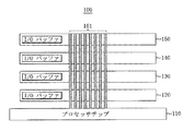
図1は、本発明の第1実施形態による積層半導体メモリ装置を含むメモリシステム100を示す簡略化された断面図である。
Hereinafter, preferred embodiments of the present invention will be described with reference to the accompanying drawings.
FIG. 1 is a simplified cross-sectional view illustrating a
図1に示すように、メモリシステム100は、プロセッサチップ110、メモリチップ120,130,140,150及び貫通電極(TSV)161を含む。メモリチップ120,130,140,150は、プロセッサチップ110の上部に積層されていて、積層半導体メモリ装置(stacked memory device)を構成する。貫通電極161は、各々のメモリチップ120,130,140,150をすべて貫通し、プロセッサチップ110に接続される。メモリチップ120,130,140,150は、各々のメモリチップ120,130,140,150の全部又は一部と貫通電極161の各々との間に結合される入出力バッファI/OBUFFERSを含む。入出力バッファI/OBUFFERSは、貫通電極161の状態に基づいて選択的に活性化される。
As shown in FIG. 1, the
図2は、図1のメモリシステム100に含まれたメモリチップの構造の一例を示す平面図である。
FIG. 2 is a plan view showing an example of the structure of a memory chip included in the
図2に示すように、メモリチップ120aは、貫通電極161aとメモリバンク121,122,123,124とで構成されたメモリコアを含む。図1に示すように、メモリバンク121,122,123,124と貫通電極161aとの間には入出力バッファI/OBUFFERSが接続されているが、図2では説明の便宜上省略した。メモリバンク121,122,123,124上には、貫通電極161とメモリバンク121,122,123,124内にある回路ブロックとを電気的に接続する内部電極が配置されている。図2では便宜上メモリバンクごとに1つの内部電極が図示されている。また、図2では、貫通電極161がメモリチップ120,130,140,150の中間部分に配置されているが、貫通電極161はメモリチップ120,130,140,150の任意の位置に配置される。
As shown in FIG. 2, the
図3は、図1のメモリシステムの3次元構造を示す簡略化された透視図である。 FIG. 3 is a simplified perspective view illustrating the three-dimensional structure of the memory system of FIG.
図3に示すように、メモリシステム100aは、貫通電極161によって電気的に接続されたプロセッサチップ110及びメモリチップ120,130,140,150を含む。図3には2行で配置された貫通電極161が図示されているが、メモリシステム100aは任意の個数の貫通電極を有することができる。
As shown in FIG. 3, the
図4は、本発明の第2実施形態による積層半導体メモリ装置を含むメモリシステム200を示す断面図である。
図4に示すように、メモリシステム200は、プロセッサチップ210及びプロセッサチップ210の上部に積層されたメモリチップ220,230,240,250で構成された積層半導体メモリ装置を含む。プロセッサチップ210はメモリコントローラ211を含むことができる。
FIG. 4 is a cross-sectional view showing a
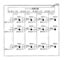
As shown in FIG. 4, the
第1メモリチップ220はプロセッサチップ210の上部に積層されており、第2メモリチップ230は第1メモリチップ220の上部に積層されており、第3メモリチップ240は第2メモリチップ230の上部に積層されており、第4メモリチップ250は第3メモリチップ240の上部に積層されている。貫通電極TSV1,TSV2,TSV3,TSV4は、第4メモリチップ250から第1メモリチップ220までを貫通してプロセッサチップ210に接続される。
The
第1乃至第4入出力バッファ221,222,223,224は、第1メモリチップ220内に含まれていて、第1乃至第4貫通電極TSV1,TSV2,TSV3,TSV4に各々接続されて4ビット信号である第1バッファイネーブル信号EN_BUF_1<0:3>により選択的に活性化される。
The first to fourth input /
第5乃至第8入出力バッファ231,232,233,234は、第2メモリチップ230内に含まれていて、第1乃至第4貫通電極TSV1,TSV2,TSV3,TSV4に各々接続されて4ビット信号である第2バッファイネーブル信号EN_BUF_2<0:3>により選択的に活性化される。
The fifth to eighth input /
第9乃至第12入出力バッファ241,242,243,244は、第3メモリチップ240内に含まれていて、第1乃至第4貫通電極TSV1,TSV2,TSV3,TSV4に各々接続されて4ビット信号である第3バッファイネーブル信号EN_BUF_3<0:3>により選択的に活性化される。
The ninth to twelfth input /
第13乃至第16入出力バッファ251,252,253,254は、第4メモリチップ250内に含まれていて、第1乃至第4貫通電極TSV1,TSV2,TSV3,TSV4に各々接続されて4ビット信号である第4バッファイネーブル信号EN_BUF_4<0:3>により選択的に活性化される。
The thirteenth to sixteenth input /
図4のメモリシステムは、第2貫通電極TSV2のDP1地点に断路(open)などの欠陥を有し、第4貫通電極TSV4のDP2地点に欠陥を有する。第2貫通電極TSV2のDP1とプロセッサチップ210との間では通信が可能である。よって、欠陥を有する第2貫通電極TSV2に接続された入出力バッファ222,232,242,252のうち欠陥発生地点DP1のすぐ下に位置した第1メモリチップ220に含まれた第2入出力バッファ222が活性化される。また、第4貫通電極TSV4のDP2とプロセッサチップ210との間では通信が可能である。よって、欠陥を有する第4貫通電極TSV4に接続された入出力バッファ224,234,244,254のうち欠陥発生地点DP2のすぐ下に位置した第3メモリチップ240に含まれた第12入出力バッファ244が活性化される。
The memory system of FIG. 4 has a defect such as an open circuit at the DP1 point of the second through electrode TSV2, and has a defect at the DP2 point of the fourth through electrode TSV4. Communication is possible between DP1 of the second through silicon via TSV2 and the
また、第1メモリチップ320に含まれた第2入出力バッファ322がすでに活性化されたため、第1貫通電極TSV1に接続された入出力バッファ221,231,241,251のうち第2メモリチップ230に含まれた第5入出力バッファ231が活性化される。また、第3メモリチップ240に含まれた第12入出力バッファ244がすでに活性化されたため、第3貫通電極TSV3に接続された入出力バッファ223,233,243,253のうち第4メモリチップ250に含まれた第15入出力バッファ253が活性化される。
In addition, since the second input /
図5は、本発明の第3実施形態による積層半導体メモリ装置を含むメモリシステムを示す断面図である。 FIG. 5 is a cross-sectional view illustrating a memory system including the stacked semiconductor memory device according to the third embodiment of the present invention.
図5に示すように、メモリシステム200aは、プロセッサチップ210a及びプロセッサチップ210aの上部に積層されたメモリチップ220a,230a,240a,250aで構成された積層半導体メモリ装置を含む。プロセッサチップ210aはメモリコントローラ211を含むことができる。貫通電極TSV1,TSV2,TSV3,TSV4は、第4メモリチップ250aから第1メモリチップ220aまでを貫通してプロセッサチップ210aに接続される。
As shown in FIG. 5, the
図5の積層半導体メモリ装置及び積層半導体メモリ装置を含むメモリシステムにおいて、メモリチップ220a,230a,240a,250aの各々の内部にバッファ制御回路が含まれている。第1メモリチップ220a内に含まれた第1バッファ制御回路225は、第1バッファイネーブル信号EN_BUF_1を生成し、第1メモリチップ220a内に含まれた入出力バッファ221,222,223,224を活性化または不活性化させる。第2メモリチップ230a内に含まれた第2バッファ制御回路235は、第2バッファイネーブル信号EN_BUF_2を生成し、第2メモリチップ230a内に含まれた入出力バッファ231,232,233,234を活性化または不活性化させる。第3メモリチップ240a内に含まれた第3バッファ制御回路245は、第3バッファイネーブル信号EN_BUF_3を生成し、第3メモリチップ240a内に含まれた入出力バッファ241,242,243,244を活性化または不活性化させる。第4メモリチップ250a内に含まれた第4バッファ制御回路255は、第4バッファイネーブル信号EN_BUF_4を生成し、第4メモリチップ250a内に含まれた入出力バッファ251,252,253,254を活性化または不活性化させる。
In the stacked semiconductor memory device of FIG. 5 and the memory system including the stacked semiconductor memory device, a buffer control circuit is included in each of the
図6は、図5の積層半導体メモリ装置を構成する1つのチップの構造の一例を示す簡略化された回路図である。 6 is a simplified circuit diagram showing an example of the structure of one chip constituting the stacked semiconductor memory device of FIG.
図6に示すように、第1メモリチップ220aのバッファ制御回路225は、第1接続ラインCL1を介して入出力バッファBUF11,BUF21,…,BUFn1に接続されている。入出力バッファBUF11,BUF21,…,BUFn1は、各々の貫通電極TSV11,TSV21,…,TSVn1に接続されている。バッファ制御回路225は、第2接続ラインCL2を介して入出力バッファBUF12,BUF22,…,BUFn2に接続されている。入出力バッファBUF12,BUF22,…,BUFn2は、各々の貫通電極TSV12,TSV22,…,TSVn2に接続されている。バッファ制御回路225は、第3接続ラインCL3を介して入出力バッファBUF13,BUF23,…,BUFn3に接続されている。入出力バッファBUF13,BUF23,…,BUFn3は、各々の貫通電極TSV13,TSV23,…,TSVn3に接続されている。バッファ制御回路225は、第4接続ラインCL4を介して入出力バッファBUF14,BUF24,…,BUFn4に接続されている。入出力バッファBUF14,BUF24,…,BUFn4は、各々の貫通電極TSV14,TSV24,…,TSVn4に接続されている。
As shown in FIG. 6, the
入出力バッファBUF11,BUF21,…,BUFn1は、貫通電極TSV11,TSV21,…,TSVn1を介して出力データDQ0_0,DQ0_1,…,DQ0_nを出力し、入出力バッファBUF12,BUF22,…,BUFn2は、貫通電極TSV12,TSV22,…,TSVn2を介して出力データDQ1_0,DQ1_1,…,DQ1_nを出力する。入出力バッファBUF13,BUF23,…,BUFn3は、貫通電極TSV13,TSV23,…,TSVn3を介して出力データDQ2_0,DQ2_1,…,DQ2_nを出力し、入出力バッファBUF14,BUF24,…,BUFn4は、貫通電極TSV14,TSV24,…,TSVn4を介して出力データDQ3_0,DQ3_1,…,DQ3_nを出力する。 , BUFn1 outputs output data DQ0_0, DQ0_1,..., DQ0_n through the through silicon vias TSV11, TSV21,. Output data DQ1_0, DQ1_1,..., DQ1_n are output via the electrodes TSV12, TSV22,. , BUFn3 outputs output data DQ2_0, DQ2_1,..., DQ2_n through the through silicon vias TSV13, TSV23,. Output data DQ3_0, DQ3_1,..., DQ3_n are output via the electrodes TSV14, TSV24,.
バッファ制御回路225は、4ビットである第1バッファイネーブル信号EN_BUF_1<0:3>を生成する。第1バッファイネーブル信号EN_BUF_1<0:3>の第1ビットEN_BUF_1<0>は、第1接続ラインCL1を介して入出力バッファBUF11,BUF21,…,BUFn1を活性化し、第1バッファイネーブル信号EN_BUF_1<0:3>の第2ビットEN_BUF_1<1>は、第2接続ラインCL2を介して入出力バッファBUF12,BUF22,…,BUFn2を活性化する。第1バッファイネーブル信号EN_BUF_1<0:3>の第3ビットEN_BUF_1<2>は、第3接続ラインCL3を介して入出力バッファBUF13,BUF23,…,BUFn3を活性化し、第1バッファイネーブル信号EN_BUF_1<0:3>の第4ビットEN_BUF_1<3>は、第4接続ラインCL4を介して入出力バッファBUF14,BUF24,…,BUFn4を活性化する。
The
図7及び図8は、図6の回路図に含まれたバッファ制御回路の実施形態を示す回路図である。 7 and 8 are circuit diagrams showing embodiments of the buffer control circuit included in the circuit diagram of FIG.
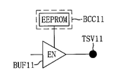
図7に示すように、バッファ制御回路225aはOTP(one time programming)を用いて実現することができる。また、図8に示すように、バッファ制御回路225bはEEPROM(Electrically erasable Programmable Read Only Memory)を用いて実現することができる。
As shown in FIG. 7, the
図9は、図5の積層半導体メモリ装置を構成する1つのチップの構造の別の一例を示す簡略化された回路図である。 FIG. 9 is a simplified circuit diagram showing another example of the structure of one chip constituting the stacked semiconductor memory device of FIG.
図9に示すように、メモリチップ220bは入出力バッファ毎に独立的にバッファ制御回路を含む。例えば、入出力バッファBUF11はバッファ制御回路BCC11によって制御され、入出力バッファBUF12はバッファ制御回路BCC12によって制御され、入出力バッファBUF13はバッファ制御回路BCC13によって制御され、入出力バッファBUF14はバッファ制御回路BCC14によって制御される。同様に、入出力バッファBUF21はバッファ制御回路BCC21によって制御され、入出力バッファBUF22はバッファ制御回路BCC22によって制御され、入出力バッファBUF23はバッファ制御回路BCC23によって制御され、入出力バッファBUF24はバッファ制御回路BCC24によって制御される。同様に、入出力バッファBUFn1はバッファ制御回路BCCn1によって制御され、入出力バッファBUFn2はバッファ制御回路BCCn2によって制御され、入出力バッファBUFn3はバッファ制御回路BCCn3によって制御され、入出力バッファBUFn4はバッファ制御回路BCCn4によって制御される。
As shown in FIG. 9, the
図10及び図11は、図9の回路図に含まれたバッファ制御回路の実施形態を示す回路図である。図10及び図11に示すように、バッファ制御回路BCC11はOTPまたはEEPROMを用いて実現することができる。 10 and 11 are circuit diagrams showing embodiments of the buffer control circuit included in the circuit diagram of FIG. As shown in FIGS. 10 and 11, the buffer control circuit BCC11 can be realized using OTP or EEPROM.
図12は、本発明の第4実施形態による積層半導体メモリ装置を含むメモリシステム300を示す断面図である。
FIG. 12 is a cross-sectional view illustrating a
図12に示すように、メモリシステム300は、プロセッサチップ310及びプロセッサチップ310の上部に積層されたメモリチップ320,330,340,350で構成された積層半導体メモリ装置を含む。プロセッサチップ310はメモリコントローラ311を含むことができる。
As shown in FIG. 12, the
第1メモリチップ320はプロセッサチップ310の上部に積層されており、第2メモリチップ330は第1メモリチップ320の上部に積層されており、第3メモリチップ340は第2メモリチップ330の上部に積層されており、第4メモリチップ350は第3メモリチップ340の上部に積層されている。貫通電極TSV1,TSV2,TSV3,TSV4は、第4メモリチップ350から第1メモリチップ320までを貫通してプロセッサチップ310に接続される。
The
第1及び第2入出力バッファ321,322は、第1メモリチップ320内に含まれていて、第1及び第2貫通電極TSV1,TSV2に各々接続されて2ビット信号である第1バッファイネーブル信号EN_BUF_1<0:1>により選択的に活性化される。
The first and second input /
第3及び第4入出力バッファ331,332は、第2メモリチップ330内に含まれていて、第3及び第4貫通電極TSV3,TSV4に各々接続されて2ビット信号である第2バッファイネーブル信号EN_BUF_2<0:1>により選択的に活性化される。
The third and fourth input /
第5及び第6入出力バッファ341,342は、第3メモリチップ340内に含まれていて、第1及び第2貫通電極TSV1,TSV2に各々接続されて2ビット信号である第3バッファイネーブル信号EN_BUF_3<0:1>により選択的に活性化される。
The fifth and sixth input /
第7及び第8入出力バッファ351,352は、第4メモリチップ350内に含まれていて、第3及び第4貫通電極TSV3,TSV4に各々接続されて2ビット信号である第4バッファイネーブル信号EN_BUF_4<0:1>により選択的に活性化される。
The seventh and eighth input /
図4の実施形態とは異なって、図12の積層半導体メモリ装置を含むメモリシステムのメモリチップ320,330,340,350は、各々の貫通電極TSV1,TSV1,TSV3,TSV4のすべてに接続せず、貫通電極TSV1,TSV1,TSV3,TSV4のうちの2つの貫通電極に接続される。
Unlike the embodiment of FIG. 4, the
図12のメモリシステムは、第2貫通電極TSV2のDP1地点において断路(open)などの欠陥を有し、第4貫通電極TSV4のDP2地点において欠陥を有する。第2貫通電極TSV2のDP1とプロセッサチップ310との間では通信が可能である。よって、欠陥を有する第2貫通電極TSV2に接続された入出力バッファ322,342のうち欠陥発生地点DP1のすぐ下に位置した第1メモリチップ320に含まれた第2入出力バッファ322が活性化される。また、第4貫通電極TSV4のDP2とプロセッサチップ310の間では通信が可能である。よって、欠陥を有する第4貫通電極TSV4に接続された入出力バッファ332,352のうち欠陥発生地点DP2のすぐ下に位置した第2メモリチップ240に含まれた第4入出力バッファ332が活性化される。
The memory system of FIG. 12 has a defect such as an open circuit at the DP1 point of the second through electrode TSV2, and has a defect at the DP2 point of the fourth through electrode TSV4. Communication is possible between DP1 of the second through silicon via TSV2 and the
また、第1メモリチップ320に含まれた第2入出力バッファ322がすでに活性化されたため、第1貫通電極TSV1に接続された入出力バッファ321,341のうち第3メモリチップ340に含まれた第5入出力バッファ341が活性化される。また、第2メモリチップ330に含まれた第4入出力バッファ332がすでに活性化されたため、第3貫通電極TSV3に接続された入出力バッファ331,351のうち第4メモリチップ350に含まれた第7入出力バッファ351が活性化される。
Further, since the second input /
図13は、本発明の第5実施形態による積層半導体メモリ装置を含むメモリシステム400を示す断面図である。
FIG. 13 is a cross-sectional view illustrating a
図13に示すように、メモリシステム400はプロセッサチップ410及びプロセッサチップ410の上部に積層されたメモリチップ420,430,440,450で構成された積層半導体メモリ装置を含む。プロセッサチップ410はメモリコントローラ411を含むことができる。
As shown in FIG. 13, the
第1メモリチップ420はプロセッサチップ410の上部に積層されており、第2メモリチップ430は第1メモリチップ420の上部に積層されており、第3メモリチップ440は第2メモリチップ430の上部に積層されており、第4メモリチップ450は第3メモリチップ440の上部に積層されている。貫通電極TSV11,TSV12,TSV13,TSV14,TSV15,TSV16,TSV17,TSV18は、第4メモリチップ450から第1メモリチップ420までを貫通してプロセッサチップ410に接続される。貫通電極TSV11,TSV12,TSV13,TSV14はアドレス/コマンドADD/CMDの伝送を行い、貫通電極TSV15,TSV16,TSV17,TSV18はデータDQの伝送を行う。
The
第1乃至第4入出力バッファ421,422,423,424は、第1メモリチップ420内に含まれていて、第1乃至第4貫通電極TSV11,TSV12,TSV13,TSV14に各々接続されて4ビット信号である第1バッファイネーブル信号EN_ABUF_1<0:3>により選択的に活性化される。第5乃至第8入出力バッファ425,426,427,428は、第1メモリチップ420内に含まれていて、第5乃至第8貫通電極TSV15,TSV16,TSV17,TSV18に各々接続されて4ビット信号である第2バッファイネーブル信号EN_DBUF_1<0:3>により選択的に活性化される。
第9乃至第12入出力バッファ431,432,433,434は、第2メモリチップ430内に含まれていて、第1乃至第4貫通電極TSV11,TSV12,TSV13,TSV14に各々接続されて4ビット信号である第3バッファイネーブル信号EN_ABUF_2<0:3>により選択的に活性化される。第13乃至第16入出力バッファ435,436,437,438は、第2メモリチップ430内に含まれていて、第5乃至第8貫通電極TSV15,TSV16,TSV17,TSV18に各々接続されて4ビット信号である第4バッファイネーブル信号EN_DBUF_2<0:3>により選択的に活性化される。
The first to fourth input /
The ninth to twelfth input /
第17乃至第20入出力バッファ441,442,443,444は、第3メモリチップ440内に含まれていて、第1乃至第4貫通電極TSV11,TSV12,TSV13,TSV14に各々接続されて4ビット信号である第5バッファイネーブル信号EN_ABUF_3<0:3>により選択的に活性化される。第21乃至第24入出力バッファ445,446,447,448は、第3メモリチップ440内に含まれていて、第5乃至第8貫通電極TSV15,TSV16,TSV17,TSV18に各々接続されて4ビット信号である第6バッファイネーブル信号EN_DBUF_3<0:3>により選択的に活性化される。
The 17th to 20th input /
第25乃至第28入出力バッファ451,452,453,454は、第4メモリチップ450内に含まれていて、第1乃至第4貫通電極TSV11,TSV12,TSV13,TSV14に各々接続されて4ビット信号である第7バッファイネーブル信号EN_ABUF_4<0:3>により選択的に活性化される。第29乃至第32入出力バッファ455,456,457,458は、第4メモリチップ450内に含まれていて、第5乃至第8貫通電極TSV15,TSV16,TSV17,TSV18に各々接続されて4ビット信号である第8バッファイネーブル信号EN_DBUF_4<0:3>により選択的に活性化される。
The 25th to 28th input /
図13の実施形態において、第1バッファイネーブル信号EN_ABUF_1<0:3>、第3バッファイネーブル信号EN_ABUF_2<0:3>、第5バッファイネーブル信号EN_ABUF_3<0:3>、及び第7バッファイネーブル信号EN_ABUF_4<0:3>は、コマンド/アドレスのための第1乃至第4貫通電極TSV11,TSV12,TSV13,TSV14に接続された入出力バッファを制御する。第2バッファイネーブル信号EN_DBUF_1<0:3>、第4バッファイネーブル信号EN_DBUF_2<0:3>、第6バッファイネーブル信号EN_DBUF_3<0:3>、及び第8バッファイネーブル信号EN_DBUF_4<0:3>は、データのための第5乃至第8貫通電極TSV15,TSV16,TSV17,TSV18に接続された入出力バッファを制御する。 In the embodiment of FIG. 13, the first buffer enable signal EN_ABUF_1 <0: 3>, the third buffer enable signal EN_ABUF_2 <0: 3>, the fifth buffer enable signal EN_ABUF_3 <0: 3>, and the seventh buffer enable signal EN_ABUF_4. <0: 3> controls the input / output buffers connected to the first to fourth through electrodes TSV11, TSV12, TSV13, and TSV14 for commands / addresses. The second buffer enable signal EN_DBUF_1 <0: 3>, the fourth buffer enable signal EN_DBUF_2 <0: 3>, the sixth buffer enable signal EN_DBUF_3 <0: 3>, and the eighth buffer enable signal EN_DBUF_4 <0: 3> An input / output buffer connected to the fifth through eighth through electrodes TSV15, TSV16, TSV17, and TSV18 for data is controlled.
第1メモリチップ420と第2メモリチップ430との間の地点DP1において第6貫通電極TSV16が欠陥を有し、第3メモリチップ440と第4メモリチップ450との間の地点DP2において第8貫通電極TSV18が欠陥を有する場合、上記第6貫通電極TSV16に接続される第1メモリチップ420の第6入出力バッファ426が活性化され、第8貫通電極TSV18に接続される第3メモリチップ440の第24入出力バッファ448が活性化される。
The sixth through electrode TSV16 has a defect at a point DP1 between the
また、第1メモリチップ420に含まれた第6入出力バッファ426がすでに活性化されたため、第5貫通電極TSV15に接続された入出力バッファ425,435,445,455のうち第2メモリチップ430に含まれた第13入出力バッファ435が活性化される。また、第3メモリチップ440に含まれた第24入出力バッファ448がすでに活性化されたため、第7貫通電極TSV17に接続された入出力バッファ427,437,447,457のうち第4メモリチップ450に含まれた第31入出力バッファ457が活性化される。
In addition, since the sixth input /
貫通電極の欠陥からデータのマッピング(mapping)が変更されると、変更されたデータのマッピングによってアドレス/コマンドADD/CMDのマッピングも変更する。図13の実施形態において、データのための貫通電極に接続された入出力バッファのうち第5貫通電極TSV15に接続される第13入出力バッファ435が活性化され、第6貫通電極TSV16に接続される第6入出力バッファ426が活性化され、第7貫通電極TSV17に接続される第31入出力バッファ457が活性化され、第8貫通電極TSV18に接続される第24入出力バッファ448が活性化される。よって、アドレス/コマンドADD/CMDのための貫通電極に接続された入出力バッファのうち第1貫通電極TSV11に接続される第9入出力バッファ431が活性化され、第2貫通電極TSV12に接続される第2入出力バッファ422が活性化され、第3貫通電極TSV13に接続される第27入出力バッファ453が活性化され、第4貫通電極TSV14に接続される第20入出力バッファ444が活性化されることができる。
When the data mapping is changed due to the defect of the through electrode, the address / command ADD / CMD mapping is also changed by the changed data mapping. In the embodiment of FIG. 13, the thirteenth input /
図14は、本発明の第6実施形態による積層半導体メモリ装置を含むメモリシステム400aを示す断面図である。
FIG. 14 is a cross-sectional view showing a
図14のメモリシステム400aは、バッファイネーブル信号を生成するバッファ制御回路がメモリチップの各々に内蔵されている。図14のメモリシステム400aの動作は、図13に示すメモリシステム400の動作に類似するため、図14のメモリシステム400aに対する動作説明は省略する。
In the
図15は、本発明の第7実施形態による積層半導体メモリ装置を含むメモリシステム400bを示す断面図である。
FIG. 15 is a cross-sectional view illustrating a
図15のプロセッサチップ410bは、図13のプロセッサチップ410に対応する。また、メモリチップ420b,430b,440b,450bは、図13のメモリチップ420,430,440,450に対応する。図15に示すように、アドレス/コマンドADD/CMDのための貫通電極に欠陥が発生した際、データのマッピングが変更される。
The
図15のメモリシステム400bは、第2貫通電極TSV12のDP3地点及び第4貫通電極TSV14のDP4地点に欠陥を有する。アドレス/コマンドADD/CMDのための貫通電極に接続された入出力バッファのうち第1貫通電極TSV11に接続される第9入出力バッファ431が活性化され、第2貫通電極TSV12に接続される第2入出力バッファ422が活性化され、第3貫通電極TSV13に接続される第27入出力バッファ453が活性化され、第4貫通電極TSV14に接続される第20入出力バッファ444が活性化される。よって、データのための貫通電極に接続された入出力バッファのうちの第5貫通電極TSV15に接続される第13入出力バッファ435が活性化され、第6貫通電極TSV16に接続される第6入出力バッファ426が活性化され、第7貫通電極TSV17に接続される第31入出力バッファ457が活性化され、第8貫通電極TSV18に接続される第24入出力バッファ448が活性化されることができる。
The
積層半導体メモリ装置のデータのマッピングが変更されると、プロセッサチップ410はデータバスの変更されたマッピングを元通り復旧する必要がある。
When the data mapping of the stacked semiconductor memory device is changed, the
図16は、図13、図14、図15のメモリシステムにおいて、変更したデータのマッピング(mapping)を元通り復旧するリペア回路412を示す回路図である。
FIG. 16 is a circuit diagram showing a
図16に示すように、リペア回路412は貫通電極TSV15,TSV16,TSV17,TSV18に接続されたデマルチプレクサDM1,DM2,DM3,DM4を含む。リペア回路412は、制御信号CTRLに応答してデータDQ0,DQ1,DQ2,DQ3を貫通電極TSV15,TSV16,TSV17,TSV18のうちの1つに提供する。制御信号CTRLはマッピングテーブル(mapping table)に基づいて得ることができ、プロセッサチップ410がメモリチップに対してトレーニング(training)動作を行って得ることができる。
As shown in FIG. 16, the
図17は、本発明の実施形態による積層半導体メモリ装置の貫通電極欠陥リペア方法を示すフローチャートである。 FIG. 17 is a flowchart illustrating a through electrode defect repair method for a stacked semiconductor memory device according to an embodiment of the present invention.
図17に示すように、以下の段階によって積層半導体メモリ装置の貫通電極欠陥をリペアすることができる。
1.メモリチップの全部又は一部と貫通電極の各々との間に入出力バッファを結合する。
2.上記貫通電極の状態に基づいて入出力バッファを選択的に活性化する。
As shown in FIG. 17, through electrode defects of the stacked semiconductor memory device can be repaired by the following steps.
1. An input / output buffer is coupled between all or part of the memory chip and each of the through electrodes.
2. The input / output buffer is selectively activated based on the state of the through electrode.
図18は、図17の貫通電極欠陥リペア方法において、入出力バッファを選択的に活性化する段階の一例を示すフローチャートである。 FIG. 18 is a flowchart showing an example of a step of selectively activating the input / output buffer in the through electrode defect repair method of FIG.
図18に示すように、入出力バッファを選択的に活性化する段階は以下の段階を含むことができる。
1.欠陥を有する貫通電極に接続された入出力バッファのうち、欠陥発生地点より下に位置する1つのメモリチップに含まれた入出力バッファを活性化する。
2.欠陥を有しない貫通電極に接続された入出力バッファを活性化する。
As shown in FIG. 18, the step of selectively activating the input / output buffer may include the following steps.
1. Among the input / output buffers connected to the through electrode having a defect, the input / output buffer included in one memory chip located below the defect occurrence point is activated.
2. The input / output buffer connected to the through electrode having no defect is activated.
図19は、図17の貫通電極欠陥リペア方法において、入出力バッファを選択的に活性化する段階の別の一例を示すフローチャートである。 FIG. 19 is a flowchart showing another example of the step of selectively activating the input / output buffer in the through electrode defect repair method of FIG.
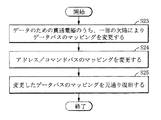
図19に示すように、入出力バッファを選択的に活性化する段階は以下の段階を含むことができる。
1.上記データのための貫通電極のうちの一部の欠陥によりデータバスのマッピング(mapping)を変更する。
2.アドレス/コマンドバスのマッピングを変更する。
As shown in FIG. 19, the step of selectively activating the input / output buffer may include the following steps.
1. The mapping of the data bus is changed due to some defects in the through electrodes for the data.
2. Change the address / command bus mapping.
本発明は、積層半導体メモリ装置を含むメモリシステムに適用可能である。
上述では、本発明の好ましい実施形態を参照して説明したが、当該技術分野の熟練した当業者は、添付の特許請求範囲に記載された本発明の思想及び領域から逸脱しない範囲で、本発明を多様に修正及び変更することができる。
The present invention is applicable to a memory system including a stacked semiconductor memory device.
Although the foregoing has been described with reference to preferred embodiments of the invention, those skilled in the art will recognize that the invention is within the scope and spirit of the invention as defined by the appended claims. Various modifications and changes can be made.
100,200,300,400 メモリシステム
110,210,310,410 プロセッサチップ
111,211,311,411 メモリコントローラ
120,130,140,150 メモリチップ
220,230,240,250 メモリチップ
320,330,340,350 メモリチップ
420,430,440,450 メモリチップ
100, 200, 300, 400
Claims (25)
前記メモリチップを貫通する複数の貫通電極(TSV)と、
少なくとも2つの前記メモリチップと1つの前記貫通電極との間に結合され、前記貫通電極の欠陥発生位置に基づいて選択的に活性化される入出力バッファと、
を含むことを特徴とする積層半導体メモリ装置。 A plurality of stacked memory chips;
A plurality of through-electrodes (TSV) penetrating the memory chip;
An input / output buffer coupled between at least two memory chips and one through electrode, and selectively activated based on a defect occurrence position of the through electrode;
A stacked semiconductor memory device comprising:
前記メモリチップの内部に含まれることを特徴とする請求項1に記載の積層半導体メモリ装置。 The input / output buffer is
The stacked semiconductor memory device according to claim 1, wherein the stacked semiconductor memory device is included in the memory chip.
前記貫通電極の欠陥発生位置に基づいて前記メモリチップの各々の内部にある入出力バッファをイネーブルさせるバッファ制御回路を含むことを特徴とする請求項1に記載の積層半導体メモリ装置。 Each of the memory chips is
2. The stacked semiconductor memory device according to claim 1, further comprising: a buffer control circuit that enables an input / output buffer in each of the memory chips based on a defect occurrence position of the through electrode.
前記貫通電極の欠陥発生位置に基づいて前記メモリチップの各々の内部にある入出力バッファをイネーブルさせるバッファ制御回路を前記入出力バッファ毎に独立的に有することを特徴とする請求項1に記載の積層半導体メモリ装置。 Each of the memory chips is
The buffer control circuit for enabling an input / output buffer in each of the memory chips based on a defect occurrence position of the through electrode independently for each of the input / output buffers. Stacked semiconductor memory device.
アドレス/コマンドのための複数の貫通電極とデータのための複数の貫通電極を含む場合、前記アドレス/コマンドのための貫通電極のうちの一部の欠陥によってアドレス/コマンドバスのマッピングが変更された場合、データバスのマッピングを変更することを特徴とする請求項1に記載の積層半導体メモリ装置。 The stacked semiconductor memory device includes:
In the case of including a plurality of through electrodes for address / command and a plurality of through electrodes for data, mapping of the address / command bus is changed due to a defect in a part of the through electrodes for address / command. 2. The stacked semiconductor memory device according to claim 1, wherein the data bus mapping is changed.
前記プロセッサチップの上部に積層された複数のメモリチップと、
前記メモリチップをすべて貫通し、前記プロセッサチップに接続された複数の貫通電極(TSV)と、
前記メモリチップの少なくとも2つと前記貫通電極の各々との間に結合され、前記貫通電極の欠陥発生位置に基づいて選択的に活性化される入出力バッファと、
を含むことを特徴とするメモリシステム。 A processor chip,
A plurality of memory chips stacked on top of the processor chip;
A plurality of through-electrodes (TSVs) penetrating all of the memory chip and connected to the processor chip;
Wherein coupled between the memory of at least two chips and each of the through electrode, and the input and output buffers are selectively activated based on defect positions of the through electrode,
A memory system comprising:
前記貫通電極の欠陥発生位置に基づいて前記入出力バッファを選択的に活性化する段階と、
を含むことを特徴とする積層半導体メモリ装置の貫通電極欠陥リペア方法。 A step of respectively coupling the output buffer between the at least two memory chips and one through the electrodes,
Selectively activating the input / output buffer based on a defect occurrence position of the through electrode;
A through electrode defect repair method for a stacked semiconductor memory device, comprising:
前記メモリチップの内部に形成されることを特徴とする請求項16に記載の積層半導体メモリ装置の貫通電極欠陥リペア方法。 The input / output buffer is
The method for repairing a through electrode defect in a stacked semiconductor memory device according to claim 16, wherein the defect is formed inside the memory chip.
欠陥を有する貫通電極に接続された入出力バッファのうち欠陥を有する貫通電極の欠陥ポイントより下に位置した1つのメモリチップに含まれた入出力バッファを活性化する段階と、
欠陥を有しない貫通電極に接続された入出力バッファを活性化する段階と、
を含むことを特徴とする請求項16に記載の積層半導体メモリ装置の貫通電極欠陥リペア方法。 Selectively activating the input / output buffer comprises:
Activating an input / output buffer included in one memory chip located below a defect point of the defective through electrode among input / output buffers connected to the defective through electrode;
Activating an input / output buffer connected to a through electrode without a defect;
The method of repairing a through electrode defect in a stacked semiconductor memory device according to claim 16, comprising:
データのための貫通電極のうちの少なくとも1つの欠陥によってデータバスのマッピングを変更する段階と、
アドレス/コマンドバスのマッピングを変更する段階と、
を含むことを特徴とする請求項16に記載の積層半導体メモリ装置の貫通電極欠陥リペア方法。 Selectively activating the input / output buffer comprises:
And changing the mapping of the data bus by the at least one defect of the through electrode for data,
Changing the address / command bus mapping;
The method of repairing a through electrode defect in a stacked semiconductor memory device according to claim 16, comprising:
前記変更されたデータバスのマッピングを元通り復旧する段階をさらに含むことを特徴とする請求項20に記載の積層半導体メモリ装置の貫通電極欠陥リペア方法。 Selectively activating the input / output buffer comprises:
21. The method of claim 20, further comprising restoring the changed data bus mapping to the original state.
前記複数のメモリチップの各々に配置された複数の入出力バッファと、
前記メモリチップを介して前記第1方向に伸びる複数の貫通電極(TSV)と、
を含み、
前記複数の貫通電極の各々は前記複数の入出力バッファのうちの少なくとも2つと結合され、前記複数の入出力バッファは前記複数の貫通電極のうちの少なくとも1つに欠陥が存在した際、前記欠陥の発生位置に基づいて選択的に活性化されることを特徴とする積層半導体メモリ装置。 A plurality of memory chips stacked in a first direction;
A plurality of input / output buffers disposed in each of the plurality of memory chips;
A plurality of through electrodes (TSV) extending in the first direction through the memory chip;
Including
Each of the plurality of through electrodes is coupled to at least two of the plurality of input / output buffers, and when the plurality of input / output buffers has a defect in at least one of the plurality of through electrodes, the defect A stacked semiconductor memory device, wherein the stacked semiconductor memory device is selectively activated based on a generation position of the semiconductor memory.
Applications Claiming Priority (2)
| Application Number | Priority Date | Filing Date | Title |
|---|---|---|---|
| KR10-2010-0051733 | 2010-06-01 | ||
| KR1020100051733A KR101728068B1 (en) | 2010-06-01 | 2010-06-01 | Stacked semiconductor memory device, memory system including the same, and method of repairing defects of through silicon vias |
Publications (3)
| Publication Number | Publication Date |
|---|---|
| JP2011253607A JP2011253607A (en) | 2011-12-15 |
| JP2011253607A5 JP2011253607A5 (en) | 2014-06-05 |
| JP5982097B2 true JP5982097B2 (en) | 2016-08-31 |
Family
ID=45022037
Family Applications (1)
| Application Number | Title | Priority Date | Filing Date |
|---|---|---|---|
| JP2011121586A Active JP5982097B2 (en) | 2010-06-01 | 2011-05-31 | Multilayer semiconductor memory device, memory system including the same, and defect repair method for through electrode |
Country Status (5)
| Country | Link |
|---|---|
| US (1) | US8654593B2 (en) |
| JP (1) | JP5982097B2 (en) |
| KR (1) | KR101728068B1 (en) |
| CN (1) | CN102270504B (en) |
| TW (1) | TWI532051B (en) |
Families Citing this family (30)
| Publication number | Priority date | Publication date | Assignee | Title |
|---|---|---|---|---|
| JP6083576B2 (en) * | 2011-12-23 | 2017-02-22 | インテル・コーポレーション | Memory device, method and system |
| KR20130098681A (en) | 2012-02-28 | 2013-09-05 | 삼성전자주식회사 | Semiconductor memory device |
| US9312257B2 (en) | 2012-02-29 | 2016-04-12 | Semiconductor Energy Laboratory Co., Ltd. | Semiconductor device |
| CN104205233B (en) * | 2012-03-30 | 2017-06-23 | 英特尔公司 | The built-in self-test of the memory architecture for stacking |
| JP2014063974A (en) * | 2012-08-27 | 2014-04-10 | Ps4 Luxco S A R L | Chip laminate, semiconductor device including chip laminate and semiconductor device manufacturing method |
| TWI501361B (en) | 2012-12-27 | 2015-09-21 | Ind Tech Res Inst | Through silicon via repair circuit |
| US9679615B2 (en) | 2013-03-15 | 2017-06-13 | Micron Technology, Inc. | Flexible memory system with a controller and a stack of memory |
| US8890607B2 (en) | 2013-03-15 | 2014-11-18 | IPEnval Consultant Inc. | Stacked chip system |
| US9136843B2 (en) | 2013-04-21 | 2015-09-15 | Industrial Technology Research Institute | Through silicon via repair circuit of semiconductor device |
| US9170296B2 (en) | 2013-08-06 | 2015-10-27 | Globalfoundries U.S.2 Llc | Semiconductor device defect monitoring using a plurality of temperature sensing devices in an adjacent semiconductor device |
| KR102104578B1 (en) * | 2013-08-30 | 2020-04-27 | 에스케이하이닉스 주식회사 | SEMICONDUCTOR APPARATUS WITH Data Bit Inversion |
| KR102111742B1 (en) | 2014-01-14 | 2020-05-15 | 삼성전자주식회사 | Stacked semiconductor package |
| KR101583939B1 (en) | 2014-06-10 | 2016-01-22 | 한양대학교 에리카산학협력단 | Semiconductor device comprising repairable penetration electrode |
| KR102125340B1 (en) | 2014-06-19 | 2020-06-23 | 삼성전자주식회사 | Integrated circuit having main route and detour route for signal transmission, and integrated circuit package therewith |
| KR20160006991A (en) * | 2014-07-10 | 2016-01-20 | 에스케이하이닉스 주식회사 | Semiconductor apparatus including a plurality of channels and through-vias |
| KR101503737B1 (en) * | 2014-07-15 | 2015-03-20 | 연세대학교 산학협력단 | Semiconductor device |
| KR102313949B1 (en) * | 2014-11-11 | 2021-10-18 | 삼성전자주식회사 | Stack semiconductor device and memory device including the same |
| TWI556247B (en) | 2014-11-12 | 2016-11-01 | 財團法人工業技術研究院 | Fault-tolerance through silicon via interface and controlling method thereof |
| US9627088B2 (en) * | 2015-02-25 | 2017-04-18 | Ememory Technology Inc. | One time programmable non-volatile memory and read sensing method thereof |
| US10832127B2 (en) * | 2015-11-30 | 2020-11-10 | Samsung Electronics Co., Ltd. | Three-dimensional integration of neurosynaptic chips |
| US10763861B2 (en) * | 2016-02-13 | 2020-09-01 | HangZhou HaiCun Information Technology Co., Ltd. | Processor comprising three-dimensional memory (3D-M) array |
| KR102451996B1 (en) * | 2016-03-31 | 2022-10-07 | 삼성전자주식회사 | Reception interface circuit for self-training of a reference voltage and memory system including the same |
| KR102416942B1 (en) * | 2017-11-13 | 2022-07-07 | 에스케이하이닉스 주식회사 | Stacked semiconductor apparatus and semiconductor system |
| KR102498883B1 (en) * | 2018-01-31 | 2023-02-13 | 삼성전자주식회사 | Semiconductor device including through electrodes distributing current |
| KR102471416B1 (en) * | 2018-05-23 | 2022-11-29 | 에스케이하이닉스 주식회사 | Semiconductor device and memory module including the same |
| US20200006306A1 (en) * | 2018-07-02 | 2020-01-02 | Shanghai Denglin Technologies Co. Ltd | Configurable random-access memory (ram) array including through-silicon via (tsv) bypassing physical layer |
| CN109817540B (en) * | 2019-01-30 | 2021-06-08 | 上海华虹宏力半导体制造有限公司 | Wafer detection defect classification method |
| KR20210034784A (en) * | 2019-09-23 | 2021-03-31 | 삼성전자주식회사 | Solid state drive device and method for fabricating the same |
| US10916489B1 (en) * | 2019-10-02 | 2021-02-09 | Micron Technology, Inc. | Memory core chip having TSVS |
| US11393790B2 (en) * | 2019-12-06 | 2022-07-19 | Micron Technology, Inc. | Memory with TSV health monitor circuitry |
Family Cites Families (14)
| Publication number | Priority date | Publication date | Assignee | Title |
|---|---|---|---|---|
| JP2004095799A (en) * | 2002-08-30 | 2004-03-25 | Toshiba Corp | Semiconductor device and method of manufacturing the same |
| JP4063796B2 (en) | 2004-06-30 | 2008-03-19 | 日本電気株式会社 | Multilayer semiconductor device |
| WO2007032184A1 (en) * | 2005-08-23 | 2007-03-22 | Nec Corporation | Semiconductor device, semiconductor chip, method for testing wiring between chips and method for switching wiring between chips |
| JP4708176B2 (en) | 2005-12-08 | 2011-06-22 | エルピーダメモリ株式会社 | Semiconductor device |
| US7494846B2 (en) * | 2007-03-09 | 2009-02-24 | Taiwan Semiconductor Manufacturing Company, Ltd. | Design techniques for stacking identical memory dies |
| KR100909902B1 (en) * | 2007-04-27 | 2009-07-30 | 삼성전자주식회사 | Flash memory device and Flash memory system |
| US7990171B2 (en) | 2007-10-04 | 2011-08-02 | Samsung Electronics Co., Ltd. | Stacked semiconductor apparatus with configurable vertical I/O |
| US7816934B2 (en) * | 2007-10-16 | 2010-10-19 | Micron Technology, Inc. | Reconfigurable connections for stacked semiconductor devices |
| US8756486B2 (en) * | 2008-07-02 | 2014-06-17 | Micron Technology, Inc. | Method and apparatus for repairing high capacity/high bandwidth memory devices |
| JP5632584B2 (en) * | 2009-02-05 | 2014-11-26 | ピーエスフォー ルクスコ エスエイアールエルPS4 Luxco S.a.r.l. | Semiconductor device |
| JP5564230B2 (en) * | 2009-10-09 | 2014-07-30 | ピーエスフォー ルクスコ エスエイアールエル | Multilayer semiconductor device |
| US8866303B2 (en) * | 2010-06-17 | 2014-10-21 | Conversant Intellectual Property Management Inc. | Semiconductor device with configurable through-silicon vias |
| KR20130011138A (en) * | 2011-07-20 | 2013-01-30 | 삼성전자주식회사 | Monolithic rank and multiple rank compatible memory device |
| JP2014236186A (en) * | 2013-06-05 | 2014-12-15 | ピーエスフォー ルクスコ エスエイアールエルPS4 Luxco S.a.r.l. | Semiconductor device |
-
2010
- 2010-06-01 KR KR1020100051733A patent/KR101728068B1/en active IP Right Grant
-
2011
- 2011-04-13 US US13/085,776 patent/US8654593B2/en active Active
- 2011-05-03 TW TW100115493A patent/TWI532051B/en active
- 2011-05-30 CN CN201110141841.0A patent/CN102270504B/en active Active
- 2011-05-31 JP JP2011121586A patent/JP5982097B2/en active Active
Also Published As
| Publication number | Publication date |
|---|---|
| KR20110131976A (en) | 2011-12-07 |
| CN102270504A (en) | 2011-12-07 |
| JP2011253607A (en) | 2011-12-15 |
| US20110292742A1 (en) | 2011-12-01 |
| CN102270504B (en) | 2016-08-31 |
| TWI532051B (en) | 2016-05-01 |
| TW201201218A (en) | 2012-01-01 |
| KR101728068B1 (en) | 2017-04-19 |
| US8654593B2 (en) | 2014-02-18 |
Similar Documents
| Publication | Publication Date | Title |
|---|---|---|
| JP5982097B2 (en) | Multilayer semiconductor memory device, memory system including the same, and defect repair method for through electrode | |
| JP5209927B2 (en) | Manufacturing method of semiconductor structure | |
| US11894093B2 (en) | Stacked DRAM device and method of manufacture | |
| US10644826B2 (en) | Flexibile interfaces using through-silicon via technology | |
| KR100724653B1 (en) | Semiconductor chip, semiconductor integrated circuit device using the same, and method of selecting semiconductor chip | |
| JP2011253607A5 (en) | ||
| JP2006244689A (en) | Semiconductor memory device capable of adjusting input/output bit structure | |
| US9287268B2 (en) | Dynamic random access memory (DRAM) and production method, semiconductor packaging component and packaging method | |
| JP4674850B2 (en) | Semiconductor device | |
| US20090091962A1 (en) | Multi-chip memory device with stacked memory chips, method of stacking memory chips, and method of controlling operation of multi-chip package memory | |
| US9379063B2 (en) | Semiconductor device and semiconductor chip | |
| JP4399777B2 (en) | Semiconductor memory device, semiconductor device, and electronic device | |
| US20110242869A1 (en) | Three-dimensional stacked semiconductor integrated circuit and control method thereof | |
| KR20150106024A (en) | Stacked semiconductor apparatus and semiconductor system capable of inputting signals through various paths | |
| US20150206825A1 (en) | Semiconductor device having through-silicon via | |
| US20130314968A1 (en) | Offsetting clock package pins in a clamshell topology to improve signal integrity | |
| CN105826274A (en) | Semiconductor package method, semiconductor package piece, and method for manufacturing dynamic random access memory | |
| KR20160148344A (en) | Input/output circuit and input/output device including the same | |
| US10403331B2 (en) | Semiconductor device having a floating option pad, and a method for manufacturing the same | |
| JP5473649B2 (en) | Semiconductor device and semiconductor module | |
| KR102017809B1 (en) | Chip die and semiconductor memory device including the same | |
| JP5666030B2 (en) | Semiconductor device and semiconductor module | |
| JP2011171480A (en) | Semiconductor device | |
| JP2015220397A (en) | Semiconductor device | |
| CN117350232A (en) | Storage structure and memory |
Legal Events
| Date | Code | Title | Description |
|---|---|---|---|
| A521 | Request for written amendment filed |
Free format text: JAPANESE INTERMEDIATE CODE: A523 Effective date: 20140416 |
|
| A621 | Written request for application examination |
Free format text: JAPANESE INTERMEDIATE CODE: A621 Effective date: 20140416 |
|
| A977 | Report on retrieval |
Free format text: JAPANESE INTERMEDIATE CODE: A971007 Effective date: 20141119 |
|
| RD04 | Notification of resignation of power of attorney |
Free format text: JAPANESE INTERMEDIATE CODE: A7424 Effective date: 20141226 |
|
| A131 | Notification of reasons for refusal |
Free format text: JAPANESE INTERMEDIATE CODE: A131 Effective date: 20150106 |
|
| A521 | Request for written amendment filed |
Free format text: JAPANESE INTERMEDIATE CODE: A523 Effective date: 20150406 |
|
| A131 | Notification of reasons for refusal |
Free format text: JAPANESE INTERMEDIATE CODE: A131 Effective date: 20151005 |
|
| A521 | Request for written amendment filed |
Free format text: JAPANESE INTERMEDIATE CODE: A523 Effective date: 20160105 |
|
| TRDD | Decision of grant or rejection written | ||
| A01 | Written decision to grant a patent or to grant a registration (utility model) |
Free format text: JAPANESE INTERMEDIATE CODE: A01 Effective date: 20160704 |
|
| A61 | First payment of annual fees (during grant procedure) |
Free format text: JAPANESE INTERMEDIATE CODE: A61 Effective date: 20160801 |
|
| R150 | Certificate of patent or registration of utility model |
Ref document number: 5982097 Country of ref document: JP Free format text: JAPANESE INTERMEDIATE CODE: R150 |
|
| R250 | Receipt of annual fees |
Free format text: JAPANESE INTERMEDIATE CODE: R250 |
|
| R250 | Receipt of annual fees |
Free format text: JAPANESE INTERMEDIATE CODE: R250 |
|
| R250 | Receipt of annual fees |
Free format text: JAPANESE INTERMEDIATE CODE: R250 |
|
| R250 | Receipt of annual fees |
Free format text: JAPANESE INTERMEDIATE CODE: R250 |
|
| R250 | Receipt of annual fees |
Free format text: JAPANESE INTERMEDIATE CODE: R250 |