JP5959216B2 - Substrate transport method and substrate transport apparatus - Google Patents
Substrate transport method and substrate transport apparatus Download PDFInfo
- Publication number
- JP5959216B2 JP5959216B2 JP2012023009A JP2012023009A JP5959216B2 JP 5959216 B2 JP5959216 B2 JP 5959216B2 JP 2012023009 A JP2012023009 A JP 2012023009A JP 2012023009 A JP2012023009 A JP 2012023009A JP 5959216 B2 JP5959216 B2 JP 5959216B2
- Authority
- JP
- Japan
- Prior art keywords
- substrate
- resin
- wafer
- temperature
- suction
- Prior art date
- Legal status (The legal status is an assumption and is not a legal conclusion. Google has not performed a legal analysis and makes no representation as to the accuracy of the status listed.)
- Active
Links
- 239000000758 substrate Substances 0.000 title claims description 135
- 238000000034 method Methods 0.000 title claims description 35
- 239000011347 resin Substances 0.000 claims description 63
- 229920005989 resin Polymers 0.000 claims description 63
- 230000007246 mechanism Effects 0.000 claims description 40
- 238000012546 transfer Methods 0.000 claims description 32
- 210000000078 claw Anatomy 0.000 claims description 20
- 238000000465 moulding Methods 0.000 claims description 12
- 238000001816 cooling Methods 0.000 claims description 9
- 230000002093 peripheral effect Effects 0.000 claims description 7
- 238000001514 detection method Methods 0.000 claims description 5
- 230000007723 transport mechanism Effects 0.000 claims description 5
- 235000012431 wafers Nutrition 0.000 description 114
- 239000004820 Pressure-sensitive adhesive Substances 0.000 description 23
- 238000010438 heat treatment Methods 0.000 description 18
- 239000002390 adhesive tape Substances 0.000 description 15
- 238000000926 separation method Methods 0.000 description 13
- 239000000853 adhesive Substances 0.000 description 8
- 230000001070 adhesive effect Effects 0.000 description 8
- 239000011810 insulating material Substances 0.000 description 7
- 239000010410 layer Substances 0.000 description 6
- 239000012790 adhesive layer Substances 0.000 description 5
- 230000009477 glass transition Effects 0.000 description 5
- 238000000227 grinding Methods 0.000 description 4
- 238000012545 processing Methods 0.000 description 4
- 230000002950 deficient Effects 0.000 description 3
- 230000003028 elevating effect Effects 0.000 description 3
- 238000002955 isolation Methods 0.000 description 3
- 238000007665 sagging Methods 0.000 description 3
- 239000004065 semiconductor Substances 0.000 description 3
- 238000007493 shaping process Methods 0.000 description 3
- 230000001276 controlling effect Effects 0.000 description 2
- 230000000694 effects Effects 0.000 description 2
- 238000002474 experimental method Methods 0.000 description 2
- 238000004519 manufacturing process Methods 0.000 description 2
- 230000001681 protective effect Effects 0.000 description 2
- 238000011084 recovery Methods 0.000 description 2
- 230000002441 reversible effect Effects 0.000 description 2
- 238000004088 simulation Methods 0.000 description 2
- 229910001220 stainless steel Inorganic materials 0.000 description 2
- 239000010935 stainless steel Substances 0.000 description 2
- 230000001360 synchronised effect Effects 0.000 description 2
- XUIMIQQOPSSXEZ-UHFFFAOYSA-N Silicon Chemical compound [Si] XUIMIQQOPSSXEZ-UHFFFAOYSA-N 0.000 description 1
- XAGFODPZIPBFFR-UHFFFAOYSA-N aluminium Chemical compound [Al] XAGFODPZIPBFFR-UHFFFAOYSA-N 0.000 description 1
- 229910052782 aluminium Inorganic materials 0.000 description 1
- 230000015572 biosynthetic process Effects 0.000 description 1
- 238000004891 communication Methods 0.000 description 1
- 238000007796 conventional method Methods 0.000 description 1
- 238000010586 diagram Methods 0.000 description 1
- 239000006260 foam Substances 0.000 description 1
- 238000005187 foaming Methods 0.000 description 1
- 239000011521 glass Substances 0.000 description 1
- 238000003825 pressing Methods 0.000 description 1
- 230000001105 regulatory effect Effects 0.000 description 1
- 229910052710 silicon Inorganic materials 0.000 description 1
- 239000010703 silicon Substances 0.000 description 1
- 239000007787 solid Substances 0.000 description 1
- 238000001179 sorption measurement Methods 0.000 description 1
- 238000003860 storage Methods 0.000 description 1
- 230000007704 transition Effects 0.000 description 1
Images


Classifications
-
- H—ELECTRICITY
- H01—ELECTRIC ELEMENTS
- H01L—SEMICONDUCTOR DEVICES NOT COVERED BY CLASS H10
- H01L21/00—Processes or apparatus adapted for the manufacture or treatment of semiconductor or solid state devices or of parts thereof
- H01L21/67—Apparatus specially adapted for handling semiconductor or electric solid state devices during manufacture or treatment thereof; Apparatus specially adapted for handling wafers during manufacture or treatment of semiconductor or electric solid state devices or components ; Apparatus not specifically provided for elsewhere
- H01L21/683—Apparatus specially adapted for handling semiconductor or electric solid state devices during manufacture or treatment thereof; Apparatus specially adapted for handling wafers during manufacture or treatment of semiconductor or electric solid state devices or components ; Apparatus not specifically provided for elsewhere for supporting or gripping
- H01L21/6838—Apparatus specially adapted for handling semiconductor or electric solid state devices during manufacture or treatment thereof; Apparatus specially adapted for handling wafers during manufacture or treatment of semiconductor or electric solid state devices or components ; Apparatus not specifically provided for elsewhere for supporting or gripping with gripping and holding devices using a vacuum; Bernoulli devices
-
- H—ELECTRICITY
- H01—ELECTRIC ELEMENTS
- H01L—SEMICONDUCTOR DEVICES NOT COVERED BY CLASS H10
- H01L24/00—Arrangements for connecting or disconnecting semiconductor or solid-state bodies; Methods or apparatus related thereto
- H01L24/93—Batch processes
- H01L24/95—Batch processes at chip-level, i.e. with connecting carried out on a plurality of singulated devices, i.e. on diced chips
- H01L24/96—Batch processes at chip-level, i.e. with connecting carried out on a plurality of singulated devices, i.e. on diced chips the devices being encapsulated in a common layer, e.g. neo-wafer or pseudo-wafer, said common layer being separable into individual assemblies after connecting
-
- H—ELECTRICITY
- H01—ELECTRIC ELEMENTS
- H01L—SEMICONDUCTOR DEVICES NOT COVERED BY CLASS H10
- H01L2924/00—Indexing scheme for arrangements or methods for connecting or disconnecting semiconductor or solid-state bodies as covered by H01L24/00
- H01L2924/10—Details of semiconductor or other solid state devices to be connected
- H01L2924/11—Device type
- H01L2924/12—Passive devices, e.g. 2 terminal devices
- H01L2924/1204—Optical Diode
- H01L2924/12041—LED
-
- H—ELECTRICITY
- H01—ELECTRIC ELEMENTS
- H01L—SEMICONDUCTOR DEVICES NOT COVERED BY CLASS H10
- H01L2924/00—Indexing scheme for arrangements or methods for connecting or disconnecting semiconductor or solid-state bodies as covered by H01L24/00
- H01L2924/10—Details of semiconductor or other solid state devices to be connected
- H01L2924/11—Device type
- H01L2924/12—Passive devices, e.g. 2 terminal devices
- H01L2924/1204—Optical Diode
- H01L2924/12042—LASER
-
- H—ELECTRICITY
- H01—ELECTRIC ELEMENTS
- H01L—SEMICONDUCTOR DEVICES NOT COVERED BY CLASS H10
- H01L2924/00—Indexing scheme for arrangements or methods for connecting or disconnecting semiconductor or solid-state bodies as covered by H01L24/00
- H01L2924/15—Details of package parts other than the semiconductor or other solid state devices to be connected
- H01L2924/151—Die mounting substrate
- H01L2924/156—Material
- H01L2924/15786—Material with a principal constituent of the material being a non metallic, non metalloid inorganic material
- H01L2924/15788—Glasses, e.g. amorphous oxides, nitrides or fluorides
-
- H—ELECTRICITY
- H01—ELECTRIC ELEMENTS
- H01L—SEMICONDUCTOR DEVICES NOT COVERED BY CLASS H10
- H01L2924/00—Indexing scheme for arrangements or methods for connecting or disconnecting semiconductor or solid-state bodies as covered by H01L24/00
- H01L2924/30—Technical effects
- H01L2924/35—Mechanical effects
- H01L2924/351—Thermal stress
- H01L2924/3511—Warping
Landscapes
- Engineering & Computer Science (AREA)
- Computer Hardware Design (AREA)
- Microelectronics & Electronic Packaging (AREA)
- Power Engineering (AREA)
- Physics & Mathematics (AREA)
- Condensed Matter Physics & Semiconductors (AREA)
- General Physics & Mathematics (AREA)
- Manufacturing & Machinery (AREA)
- Container, Conveyance, Adherence, Positioning, Of Wafer (AREA)
Description
本発明は、半導体ウエハやLED(Light Emitting Diode)などの基板を搬送する基板搬送方法および基板搬送装置に係り、特に、ダイシング処理によって基板から分断されたチップのうち良品のみを樹脂でモールドして円形や四角形に成型し直し、所定の工程で加熱された当該成型基板を搬送する技術に関する。 The present invention relates to a substrate transport method and a substrate transport apparatus for transporting a substrate such as a semiconductor wafer or an LED (Light Emitting Diode), and in particular, by molding only good products out of chips separated from a substrate by a dicing process with a resin. The present invention relates to a technique of re-molding into a circle or a rectangle and conveying the molded substrate heated in a predetermined process.
近年、高密度実装の要求に伴って半導体ウエハ(以下、適宜「ウエハ」という)の厚みが、数十μmまでバックグラインド処理される傾向にある。したがって、バックグラインド処理からダイシング処理を終えるまでに表面に形成された回路やバンプが破損し、生産効率が低下している。 In recent years, with the demand for high-density mounting, the thickness of a semiconductor wafer (hereinafter referred to as “wafer” as appropriate) tends to be back-grinded to several tens of μm. Therefore, the circuits and bumps formed on the surface are damaged from the back grinding process to the dicing process, and the production efficiency is lowered.
そこで、回路形成済のウエハにバックグラインド処理を行う前にダイシング処理を行い、良品の回路形成済みのベアチップのみ選別している。これら良品のチップのみを樹脂でモールディングして基板形状に成形し直している。具体的には、次のように実施している。 Therefore, dicing processing is performed before the back-grinding processing is performed on the wafer on which the circuit has been formed, and only non-defective circuit-formed bare chips are selected. Only these non-defective chips are molded with a resin and molded into a substrate shape. Specifically, it is implemented as follows.
図21(a)に示すように、ローラRで粘着シート3を押圧してキャリア用の基板2(例えば、アルミニウムやステンレス鋼)に貼り付ける。良品のベアチップ1aの電極面を下向きにし、図21(b)に示すように、基板2上の接着シート3上に2次元アレー状に整列固定する。図21(c)に示すように、ベアチップ1a上から樹脂1bをモールドし、ウエハ形状に成型し直す。図21(d)に示すように、粘着シート3の接着力を低下させて当該成型ウエハ1を基板2から分離する。このとき、粘着シート3は、基板2側に残されている。その後、図21(e)に示すように、樹脂1bから露出している電極面側に保護シートPを貼付け、反対側からバックグラインドする。バックグラインド後に保護テープPを剥離し、図21(d)に示すように、薄型化された成形ウエハ1を支持用の粘着テープDCを介してリングフレームfに接着支持し、ベアチップを分断するダイシング工程へと搬送している(特許文献1)。
As shown in FIG. 21A, the pressure-sensitive
また、上述のような、成型された良品のベアチップのみをモールドして成型し直した成形ウエハを、非接触で温度コントロールしながら搬送することが提案および実施されている(特許文献2)。 In addition, it has been proposed and practiced to transport a molded wafer obtained by molding and remolding only a molded good bare chip as described above while controlling the temperature in a non-contact manner (Patent Document 2).
また、近年のウエハの薄型化に伴い、低下した剛性を補強するために、同形状の支持板を両面粘着テープで貼り合わせている。当該支持板は、マウント工程において、剥離される。その剥離方法は、加熱することで発砲膨張して接着力を低下または減滅させる加熱剥離性または紫外線硬化型の感圧性の粘着層を有する両面粘着テープを利用し、マウント工程の前に当該支持板付きのウエハに加熱処理にて実施している(特許文献3)。 In addition, in order to reinforce the lowered rigidity due to the recent thinning of the wafer, a support plate having the same shape is bonded with a double-sided adhesive tape. The support plate is peeled off in the mounting process. The peeling method uses a double-sided pressure-sensitive adhesive tape having a heat-releasable or UV-curable pressure-sensitive adhesive layer that expands and expands by heating to reduce or diminish the adhesive force. The heat treatment is performed on a wafer with a plate (Patent Document 3).
近年の高密度実装の要求に伴って成型ウエハの形状が大型化する傾向にある。したがって、搬送経路上で浮上させて非接触で搬送すると、増大した自重が未硬化状態の樹脂の硬度よりも上回り、基板に反りを発生させるといった問題がある。 With the recent demand for high-density mounting, the shape of the molded wafer tends to increase. Therefore, when the surface is lifted on the transport path and transported in a non-contact manner, there is a problem in that the increased weight exceeds the hardness of the uncured resin, causing the substrate to warp.
また、硬化処理を受けた樹脂であっても、後工程で加熱処理を施されると軟化する。したがって、軟化状態の樹脂も未硬化状態の樹脂と同様に、非接触状態で成型ウエハを搬送すると反りが発する。 Moreover, even if it is resin which received the hardening process, if it heat-processes by a post process, it will soften. Therefore, the softened resin, like the uncured resin, warps when the molded wafer is conveyed in a non-contact state.
また、樹脂が未硬化または軟化状態の場合、成型ウエハの反りのみならず、ウエハ外周の樹脂が、自重で僅かに裏面側に垂れる。このような樹脂の垂れは、ウエハの厚みを不均一にするので、後工程のダイシング処理においてウエハを所望のスクライブラインに沿って精度よく切断できないといったさらなる問題を生じさせている。 Further, when the resin is in an uncured or softened state, not only the warping of the molded wafer but also the resin on the outer periphery of the wafer slightly hangs down to the back side due to its own weight. Such dripping of the resin makes the thickness of the wafer non-uniform, which causes a further problem that the wafer cannot be accurately cut along a desired scribe line in a dicing process in a subsequent process.
また、軟化状態の樹脂にエアーを吹き付けると、その面が波打って凹凸が生じる場合もある。 In addition, when air is blown onto the softened resin, the surface may be undulated to cause unevenness.
また、成型ウエハは、従来の円形以外に四角形にも成型されるようになっている。従来の非接触方法で当該成型ウエハを搬送すると、当該成型ウエハの垂直軸周りに回転し易く、かつ、所定の進路を維持して搬送させることが困難になっている。したがって、搬送経路の両側縁に沿って設けた落下防止用の側壁に成型ウエハの角部が接触し、破損するといった問題も生じている。 In addition to the conventional circular shape, the molded wafer is also formed into a square shape. When the molded wafer is transported by a conventional non-contact method, it is easy to rotate around the vertical axis of the molded wafer and it is difficult to transport the molded wafer while maintaining a predetermined path. Accordingly, there is a problem that corners of the molded wafer come into contact with the side walls for preventing the fall provided along both side edges of the transport path and are damaged.
本発明はこのような事情に鑑みてなされたものであって、基板を破損させることなく、効率よく冷却しながら基板を搬送する基板搬送方法および基板搬送装置を提供することを主たる目的とする。 The present invention has been made in view of such circumstances, and a main object of the present invention is to provide a substrate transport method and a substrate transport apparatus that transport a substrate while efficiently cooling it without damaging the substrate.
この発明は、このような目的を達成するために、次のような構成をとる。
すなわち、本発明は、基板を搬送する基板搬送方法であって、
前記基板は、平面状に整列配置された複数個のチップを樹脂でモールドして成型した基板であり、
前記樹脂が加熱状態にある基板を吸着プレートで吸着保持して冷却しながら搬送する搬送する過程を含み、
加熱状態にある前記基板を搬出側テーブルから吸着プレートで吸着保持して搬送する過程で、当該基板の樹脂が自重で変形または垂れない温度まで基板を冷却し、
前記温度に達した基板を搬入側テーブルに受け渡し、当該搬入側テーブルで基板を室温まで冷却する
ことを特徴とする。
In order to achieve such an object, the present invention has the following configuration.
That is, the present invention is a substrate carrying method for carrying a substrate,
The substrate is a substrate formed by molding a plurality of chips arranged in a plane and molded with a resin,
Including a process of transporting the substrate in which the resin is in a heated state while being sucked and held by a suction plate and cooled ,
In the process of transporting the substrate in the heated state by suction holding from the carry-out side table with the suction plate, the substrate is cooled to a temperature at which the resin of the substrate does not deform or droop due to its own weight,
The substrate that has reached the temperature is delivered to a loading-side table, and the substrate is cooled to room temperature by the loading-side table .
(作用・効果) 上記方法によれば、加熱状態にある基板を吸着プレートで吸着保持しているので、カラス転移点以上またはガラス転移点以下であっても撓みやすい軟化状態にある樹脂の硬度を上回る自重の影響により生じる基板の反りが回避される。つまり、吸着プレートによって基板が吸着保持されて平坦な状態に強制される。また、吸着プレートに吸着保持されまま樹脂が冷却されるので、反りを発生させる自重を超える硬度まで樹脂を効率よく硬化させることができる。したがって、基板に反りや樹脂の垂れ、および裏面に凹凸を発生させることなく、基板裏面を平坦な状態を保ちつつ各処理部に搬送することができる。
(Operation / Effect) According to the above method, since the substrate in the heated state is sucked and held by the suction plate, the hardness of the resin in the softened state that is easily bent even if it is higher than the crow transition point or lower than the glass transition point is obtained. The substrate warpage caused by the influence of the excess weight is avoided. That is, the substrate is sucked and held by the suction plate and forced into a flat state. Further, since the resin is cooled while being adsorbed and held on the adsorption plate, the resin can be efficiently cured to a hardness exceeding its own weight that causes warping. Therefore, the back surface of the substrate can be transported to each processing unit while maintaining a flat state without causing warpage or dripping of the resin and unevenness on the back surface.
さらに、基板が吸着プレートで覆われているので、当該基板の姿勢を維持したまま所定の搬送経路に沿って確実に目的位置まで搬送することができる。したがって、搬送過程で他の構造物などに基板が接触して破損するのを回避することができる。 Furthermore, since the substrate is covered with the suction plate, the substrate can be reliably transported to the target position along a predetermined transport path while maintaining the posture of the substrate. Therefore, it is possible to avoid the substrate from coming into contact with other structures or the like during the transfer process and being damaged.
また、この発明は、このような目的を達成するために、次のような構成をとる。 The present invention has the following configuration in order to achieve such an object.
基板を搬送する基板搬送装置であって、
前記基板は、平面状に整列配置された複数個のチップを樹脂でモールドして成型した基板であり、
前記基板を吸着保持して冷却可能な吸着プレートを備えた搬送機構と、
前記基板を吸着保持して冷却するテーブルと、
前記樹脂が加熱状態にある基板を吸着プレートで吸着保持して異なる温度設定の各テーブルに搬送する過程で、該基板の樹脂が自重で変形または垂れない温度まで基板を冷却し、当該温度に達した基板を搬入側テーブルに受け渡し、当該搬入側テーブルで基板を室温まで冷却する制御部と、
を備えることを特徴とする。
A substrate transfer device for transferring a substrate,
The substrate is a substrate formed by molding a plurality of chips arranged in a plane and molded with a resin,
A transport mechanism provided with a suction plate capable of cooling by holding the substrate;
A table that holds and cools the substrate;
In the process of sucking and holding the substrate in which the resin is heated by the suction plate and transporting it to each table with different temperature settings, the substrate is cooled to a temperature at which the resin of the substrate does not deform or sag due to its own weight, and reaches that temperature. A controller that delivers the substrate to the carry-in table and cools the substrate to room temperature by the carry-in table ;
It is characterized by providing.
(作用・効果) この構成によれば、基板を吸着プレートで吸着保持した状態で冷却しながら複数台のテーブルに当該基板を搬送することができる。したがって、上記方法を好適に実施することができる。 (Operation / Effect) According to this configuration, the substrate can be transported to a plurality of tables while cooling in a state where the substrate is sucked and held by the suction plate. Therefore, the above method can be suitably performed.
なお、上記構成において、基板の温度を検出する検出器を備え、
制御部は、検出器の検出結果に応じて各テーブルからの搬出および各テーブルへの搬入のタイミングを調整することが好ましい。
In the above configuration, a detector for detecting the temperature of the substrate is provided,
It is preferable that the control unit adjusts the timing of unloading from each table and loading into each table according to the detection result of the detector.
この構成によれば、基板の自重による反りを上回る硬度に樹脂が達するのを確実に判別することができる。したがって、基板の反りを確実に回避することができる。 According to this configuration, it is possible to reliably determine that the resin reaches a hardness exceeding the warpage due to the weight of the substrate. Therefore, it is possible to reliably avoid warping of the substrate.
なお、上記構成において、前記樹脂で被覆された基板裏面の外周部分の複数箇所を支持する支持爪を備えた支持プレートと、
前記支持プレートを昇降させて支持爪上の基板を前記テーブルの載置面と、当該テーブル上方の搬出位置に移動させる駆動機構を備えることが好ましい。
In the above configuration, a support plate including support claws for supporting a plurality of locations on the outer peripheral portion of the back surface of the substrate coated with the resin;
It is preferable to include a drive mechanism that raises and lowers the support plate to move the substrate on the support claw to a placement surface of the table and a carry-out position above the table.
この構成によれば、テーブル上への基板の載置およびテーブルからの基板の搬出時に、基板裏面の外周部分を支持爪で支持しているので、基板の外周部分で発生しがちな垂れが抑制される。また、基板裏面側に進入してくる搬送機構の経路を妨げることがない。 According to this configuration, since the outer peripheral portion of the back surface of the substrate is supported by the support claws when the substrate is placed on the table and the substrate is taken out of the table, drooping that tends to occur in the outer peripheral portion of the substrate is suppressed. Is done. Further, the path of the transport mechanism entering the back side of the substrate is not obstructed.
さらに、上記構成において、テーブルは、樹脂で被覆された基板裏面の中央領域を支持する複数本のピンを備えることが好ましい。 Furthermore, in the above configuration, the table preferably includes a plurality of pins that support the central region of the back surface of the substrate coated with resin.
この構成によれば、テーブルへの基板の受け渡し時などにおいて、吸着プレートによる吸着保持が解除された場合、ピンで中央領域を支持することにより、基板の反りを抑制することができる。また、基板の外周部分を支持爪で支持し、かつ、中央領域をピンで支持することにより、基板を水平に保つことができる。したがって、基板の搬入、搬送および搬出のいずれの時点においても、当該基板を平坦に維持することが可能になる。 According to this configuration, when the suction holding by the suction plate is released at the time of delivery of the substrate to the table or the like, the warp of the substrate can be suppressed by supporting the central region with the pins. Further, the substrate can be kept horizontal by supporting the outer peripheral portion of the substrate with the support claws and supporting the central region with the pins. Therefore, it is possible to keep the substrate flat at any time of loading, transporting and unloading the substrate.
本発明の基板搬送方法および基板搬送装置によれば、複数個のチップを樹脂でモールドして成型された基板の当該樹脂が加熱されて軟化状態にあったとしても、基板を破損させることなく冷却しながら精度よく目的位置に当該基板を搬送することができる。 According to the substrate transfer method and the substrate transfer apparatus of the present invention, even if the resin of the substrate formed by molding a plurality of chips with resin is heated and softened, it is cooled without damaging the substrate. The substrate can be accurately transferred to the target position.
以下、図面を参照して本発明の実施例を説明する。 Embodiments of the present invention will be described below with reference to the drawings.
本発明の基板搬送装置は、図2に示すように、ステンレス鋼、ガラス基板またはシリコン基板からなる支持板2と同心状に両面粘着テープ3を介して貼り合わされたバックグラインド前のウエハ1を、当該支持板2から分離する支持板分離装置に備わっている。なお、支持板2は、ウエハ1と同等サイズまたはそれ以上である。
As shown in FIG. 2, the substrate transfer apparatus of the present invention includes a
ここで、ウエハ1は、次のようにして成型されている。ウエハ表面への回路形成後にダイシング処理がされたベアチップ1aを検査し、良品のベアチップ1aのみを選別する。これらベアチップ1aの電極面を下向きにし、図3に示すように、キャリア用の支持板2に貼り付けた両面粘着テープ3上に2次元アレー状に整列固定する。さらに、ベアチップ1a上から樹脂1bでモールドし、ウエハを成型している。
Here, the
図2に戻り、両面粘着テープ3は、テープ基材3aの両面に、加熱することで発泡膨張して接着力を失う加熱剥離性の粘着層3bと、紫外線の照射によって硬化して接着力が低下する紫外線硬化型または非紫外線硬化型の感圧性の粘着層3cを備えて構成されたものである。つまり、この両面粘着テープ3の粘着層3bに支持板2が貼り付けられるとともに、粘着層3cにウエハ1が貼付けられている。
Returning to FIG. 2, the double-sided pressure-sensitive
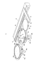
図1は本発明に係る支持板分離装置を示す平面図、図4は第3基板搬送装置の概略を示す全体斜視図、図5は第3基板搬送装置の正面図および図6は第3基板搬送装置の部分縦断側面図である。 1 is a plan view showing a support plate separating apparatus according to the present invention, FIG. 4 is an overall perspective view showing an outline of a third substrate transfer device, FIG. 5 is a front view of the third substrate transfer device, and FIG. 6 is a third substrate. It is a partial vertical side view of a conveying apparatus.
この支持体分離装置は、ワークWを収納したカセットC1およびウエハ1または支持板2を収納したカセットC2が装填されるウエハ供給/回収部4、第1ロボットアーム5を備えた第1基板搬送機構6、冷却機構7、第2ロボットアーム8を備えた第2基板搬送機構9、予備加熱テーブル10、第3基板搬送装置11、ワークWから支持板2を分離する支持板分離機構12と、支持板2が分離されたウエハ1から両面粘着テープ3を剥離除去するテープ剥離機構13と、剥離除去した両面粘着テープ3を回収するテープ回収部14、ウエハ1にマーキングを付すマーキング部15、ウエハ受渡部16、および第4ロボットアーム17を備えた第4基板搬送機構18が備えられている。以下、各機構についての具体的に説明する。
The support separating apparatus includes a wafer supply / recovery unit 4 loaded with a cassette C1 storing workpieces W and a cassette
ウエハ供給/回収部4には、供給側に2台のカセットC1および回収側に2台のカセットC2を並列して載置される。カセットC1には、ウエハ1に支持板2を貼り合わせて成るワークWが、当該支持板2を下にして複数枚を多段に水平姿勢で差込み収納されている。カセットC2の一方には、支持板2を分離されてベアチップ1aの回路面を上向きにした複数枚のウエハ1が、多段に水平姿勢で差込み収納されている。カセットC2の他方には、分離後の複数枚の支持板2が、多段に水平姿勢で差込み収納されている。
In the wafer supply / recovery unit 4, two cassettes C1 are placed in parallel on the supply side and two cassettes C2 are placed in parallel on the collection side. In the cassette C1, a workpiece W formed by bonding the
第1基板搬送機構6に備えられた第1ロボットアーム5は、上下に反転および水平に進退移動可能に構成されるとともに、全体が旋回および昇降可能になっている。この第1ロボットアーム5の先端には、馬蹄形をした真空吸着式のワーク保持部5aが備えられている。さらに、ワーク保持部5aには、アライメント機構が備わっている。例えば、先端側の2カ所に上向きの保持部が形成されており、基端側の角部に2本の可動ピンが備わっている。当該可動ピンを移動させることにより、保持部と協動してワークWを挟み込んでアライメントおよび保持を行う。
The
冷却機構7は、吸着パッド19と冷却ユニット20から構成されている。吸着パッド19は、加熱状態にある支持板2の中央を吸着して回転する。冷却ユニット20は、吸着パッド19の上方に配備され、回転している支持板2にエアーを吹き付ける。
The cooling mechanism 7 includes a suction pad 19 and a cooling unit 20. The suction pad 19 rotates by sucking the center of the
第2基板搬送機構9に備えられた第2ロボットアーム8は、水平に進退移動可能に構成されるとともに、全体が旋回および昇降可能になっている。この第2ロボットアーム8の先端には、馬蹄形をした真空吸着式のワーク保持部8aが備えられている。
The
予備加熱テーブル10は、ワークWよりも大形で表面に微小幅(例えば1mm以下)の吸着溝の形成されたチャックテーブルである。また、予備加熱テーブル10は、断熱材で形成されており、その内部にヒータおよび表面のワークWの温度を検知する温度センサを備えている。温度センサの検出信号は、制御部80に送られる。さらに、予備加熱テーブル10は、表面を出退昇降可能にする複数本の支持ピンを備えている。支持ピンの先端は、絶縁物で構成されているか、あるいは絶縁物で被覆されている。
The preheating table 10 is a chuck table which is larger than the workpiece W and has a suction groove having a minute width (for example, 1 mm or less) on the surface. The preheating table 10 is formed of a heat insulating material, and includes a heater and a temperature sensor that detects the temperature of the workpiece W on the surface. The detection signal of the temperature sensor is sent to the
第3基板搬送装置11は、図4ないし図7に示すように、第1テーブル21、第2テーブル22およびウエハ搬送機構23が配備されている。なお、第3基板搬送装置11は、本発明の基板搬送装置に相当する。
As shown in FIGS. 4 to 7, the third
第1テーブル21は、ワークWよりも大形で表面に微小幅(例えば1mm以下)の吸着溝の形成されたチャックテーブルである。第1テーブル21は、断熱材で形成されており、その内部にヒータ24aおよび温度センサ25a(図7を参照)を備えている。なお、温度センサ25aは、テーブル表面のワークWの温度を検知して検出信号を制御部80に送る。
The first table 21 is a chuck table that is larger than the workpiece W and has a suction groove having a minute width (for example, 1 mm or less) on the surface. The 1st table 21 is formed with the heat insulating material, and is equipped with the
また、第1テーブル21の外周の複数箇所に中心向きに先細りの凹部26が設けられている。また、第1テーブル21は、流路を介して外部の真空装置と連通接続されている。また、第1テーブル21は、複数本の支持用のピン27aを装備している。
In addition, tapered
複数本のピン27aは、第1テーブル21の所定の円周上に等間隔をおいて配備されている。すなわち、これらピン27aは、可動台50aに設けられており、可動台50aに連結されたシリンダ28aによって第1テーブル21の保持面に対して出退昇降可能に構成れている。さらに、ピン27aの先端は、絶縁物で構成されているか、あるいは絶縁物で被覆されている。
The plurality of
第1テーブル21の外周には、第1テーブル21の上方でワークWを受け取る位置と第1テーブル21上にワークWを受け渡す昇降機構29aが配備されている。
On the outer periphery of the first table 21, a position for receiving the workpiece W above the first table 21 and an elevating
昇降機構29aは、第1テーブル21と同一曲率を有する円弧状のプレート30aを有する。プレート30aは、シリンダ31aによって昇降可能に構成されている。また、プレート30aには複数本の支持爪32aが配備されている。なお、プレート30aは本発明の支持プレートに相当し、シリンダ31aは駆動機構に相当する。
The elevating
支持爪32aの先端は、第1テーブル21の中心向きに先細りになっている。つまり、プレート30aを昇降させたとき、支持爪32aは、第1テーブル21の外周に設けられた凹部26内に収まる。このとき、支持爪32aの表面は、第1テーブル21の表面以下になる。なお、本実施例では、3本の支持爪32aを利用しているが、当該本数に限定されるものではく、3本以上であってもよい。
The tip of the
なお、第2テーブル22は、第1テーブル21と略同じ構造をしている。したがって、同一構造には同一番号にアルファベットの「b」を付している。 The second table 22 has substantially the same structure as the first table 21. Therefore, alphabetical letters “b” are attached to the same number in the same structure.
ウエハ搬送機構23は、水平に往復移動する可動台33、この可動台33から延伸したアーム34、当該アーム先端の装備された吸着プレート35から構成されている。
The
可動台33は、装置基台に配備されたフレーム36に敷設された2本の案内レール37に沿って左右に移動する。すなわち、図4および図5に示すように、案内レール37の一端側に配備されたモータ38によって正逆転駆動される駆動プーリ39が軸支されるとともに、他端側に遊転プーリ40が軸支されている。駆動プーリ39と遊転プーリ40とに亘って巻き掛けられたベルト41に可動台33のスライド係合部42が連結されている。したがって、ベルト41の正逆回動によって可動台33が左右に移動されるようになっている。
The movable table 33 moves to the left and right along two
吸着プレート35は、ウエハ1よりも大形で表面に微小幅(例えば1mm以下)の吸着溝の形成された断熱材で構成されている。本実施例では、吸着プレート35は、第1テーブル21および第2テーブル22よも小径に設定されている。また、吸着プレート35の外周の複数箇所に中心向きに先細りの切り欠き43が設けられている。この切り欠き43は、ウエハ1の内側に達している。また、吸着プレート35の吸着溝は、複数本の流路を介して外部の真空装置と連通接続されている。さらに、吸着プレート35は、ヒータ44および温度センサ45を備えている。なお、温度センサ45は、保持面上のウエハ1の温度を検知し、検出信号を制御部80に送る。
The
支持板分離機構12は、図8に示すように、縦壁55の背部に縦向きに配置されたレール56に沿って昇降可能な可動台57、この可動台57に高さ調節可能に支持された可動枠58、この可動枠58から前方に向けて延出されたアーム59の先端部に装着された吸着プレート60などを備えている。
As shown in FIG. 8, the support
可動台57は、ネジ軸61をモータ62によって正逆転駆動することでねじ送り昇降される。また、吸着プレート60の下面は真空吸着面に構成されるとともに、当該吸着プレート内部にはヒータ63が内蔵されている。
The movable table 57 is screwed up and down by driving the
テープ剥離機構13は、図9ないし図11に示すように、レール65に沿って前後にスライド移動可能な可動台66から下向きに延出された支持フレーム67を介して剥離ローラ68が装着されている。
As shown in FIGS. 9 to 11, the
可動台66は、モータ69で正逆転駆動されるネジ軸70によって前後水平に独立してねじ送り移動させるよう構成されている。
The movable table 66 is configured to be screw-feeded independently in the front-rear and horizontal directions by a
剥離ローラ68は、図9および図10に示すように、中空の回転軸72に装着されたプーリ73とモータ74の駆動軸に装着された駆動プーリ78とに張架された無端ベルト79によって自転可能に構成されている。また、剥離ローラ68は、図11に示すように、表面に吸引孔71設けられており、外部に配備された吸引装置に連通接続されている。なお、剥離ローラ68は、弾性体で被覆されている。
As shown in FIGS. 9 and 10, the peeling
吸引孔71は、両面粘着テープ3の剥離開始端の部分と剥離終了端に対応する位置に形成されている。剥離開始端側の吸引孔71は、テープ外周の円弧に沿った複数個の長孔に形成されている。剥離終了端側の吸引孔71は、1個の長孔が形成されている。なお、吸引孔71の形状および個数は、両面粘着テープ3の大きさや形状に応じて適宜に変更される。
The
テープ回収部14は、図10に示すように、剥離ローラ68の下方に回収ボックスとして配備されている。
As shown in FIG. 10, the
マーキング部15は、ウエハ1を吸着保持するチャックテーブル75、チャックテーブル75に吸着保持されたウエハ1に2次元コードや3次元立体コードなどのマーキングを施すレーザ装置76を備えている。
The marking
ウエハ受渡部16は、ウエハ1および支持板2の裏面を吸着保持する吸着パッド77を備えている。吸着パッド77は、マーキング部15側から第4ロボットアーム17への受け渡し位置にスライド移動するとともに、昇降するように構成されている。
The
第4基板送機構18に備えられた第4ロボットアーム17は、平に進退移動可能に構成されるとともに、全体が旋回および昇降可能となっている。この第4ロボットアーム17の先端には、馬蹄形をした真空吸着式のワーク保持部17aが備えられている。
The
次に、ウエハ搬送装置を備えた上記支持板分離装置の一連の動作について、図12〜20を参照しながら説明する。 Next, a series of operations of the support plate separating apparatus provided with the wafer transfer apparatus will be described with reference to FIGS.
先ず、図7に示す操作部を操作して各種設定を行う。例えば、予備加熱テーブル10のヒータの加熱温度、支持板分離機構12のヒータ63の加熱温度、第1テーブル21、第2テーブル22および吸着プレート35の各ヒータの加熱温度並びに時間等の各条件を設定する。
First, various settings are performed by operating the operation unit shown in FIG. For example, the heating temperature of the preheating table 10, the heating temperature of the
予備加熱テーブル10の加熱温度は、例えば次のようにして求められる。ウエハ1と支持板2を両面粘着テープ3に貼り合わせるとき、貼付部材の押圧力で両面粘着テープ3および樹脂1bの少なくともいずれかが延伸される。換言すれば、貼り合わせが完了したとき、復元力が樹脂1bや両面粘着テープ3に蓄積される。したがって、この復元力の作用によりウエハ1と支持板2が一体となったワークWが僅かに反り返っているものが含まれる。そこで、ワークWの反りを修正する。つまり、ワークWが平坦となるよう、樹脂1bおよび両面粘着テープ3の少なくともいずれかを適度に軟化させる温度に設定する。この温度や時間は、使用する樹脂1bおよび両面粘着テープ3の特性によって異なるので、実験やシミュレーションなどによって予め決定される。
The heating temperature of the preheating table 10 is calculated | required as follows, for example. When the
支持分離機構12における加熱温度は、加熱剥離性の粘着層3bを有する両面粘着テープ3に応じて設定する。つまり、加熱により発泡膨張して粘着力を低減または減滅する温度に設定する。
The heating temperature in the
第1テーブル21、第2テーブル22および吸着プレート35の加熱温度は、本実施例では、例えば第1テーブル21、吸着プレート35および第2テーブル22の順に低くなるよう設定される。なお、加熱温度の設定は、当該順番に限定されるものではなく、使用する樹脂の特性、ウエハ1の形状あるいは重量などによって適宜に変更することができる。
In the present embodiment, the heating temperatures of the first table 21, the second table 22, and the
先ず、第1テーブル21の加熱温度は、支持分離機構12と協動して両面粘着テープ3の粘着層3bを発砲膨張させる温度に設定される。
First, the heating temperature of the first table 21 is set to a temperature at which the adhesive layer 3b of the double-sided
第2テーブル22の加熱温度は、ウエハ1が室温程度になるように設定される。
The heating temperature of the second table 22 is set so that the
吸着プレート35の加熱温度および時間は、第2テーブル22よりも厳格に設定される。つまり、第1テーブル21で軟化している樹脂1bと接触して直接に冷却したとき、軟化した樹脂1bが自重によりウエハ1の端縁側で垂れや変形しないなどの条件を満たす温度および時間に設定される。この条件は、使用する樹脂1bによって異なるので、実験やシミュレーションなどによって予め決定する。例えば、樹脂1bのガラス転移点の近傍、ガラス転移点を含む所定範囲などである。
The heating temperature and time of the
これら各設定条件は、制御部80に備わった記憶部81に記憶される。
Each of these setting conditions is stored in a
各条件の設定が完了すると、装置を作動させる。先ず、第1基板搬送機構6の第1ロボットアーム5が、カセットC1に向けて移動される。第1ロボットアーム5の先端のワーク保持部5aがカセットC1に収容されているワークW同士の隙間に挿入される。ワーク保持部5aは、ワークWを裏面から吸着保持して搬出する。つまり、支持板2を保持して搬出する。この搬出過程でアライメントも行う。その後、上下反転し、ウエハ1の樹脂1b面を下向きにして予備加熱テーブル10に移載する。
When the setting of each condition is completed, the apparatus is operated. First, the
このとき、予備加熱テーブル10は、ピンを保持面から突き出してワークWを受け取り、その後下降する。ワークWは、テーブル上で吸着保持され、所定温度まで加熱される。予備加熱処理の間、温度センサによってワークWの温度が検出される。ワークWが所定温度に達すると、ピンでワークWを上昇させる。この時点で、樹脂1bや両面粘着テープ3が僅かに軟化し、これら樹脂1bや両面粘着テープ3に作用している復元力が解放される。したがって、ワークWの僅かな反りが解消されて平坦になる。
At this time, the preheating table 10 projects the pin from the holding surface, receives the workpiece W, and then descends. The workpiece W is sucked and held on the table and heated to a predetermined temperature. During the preheating process, the temperature of the workpiece W is detected by the temperature sensor. When the workpiece W reaches a predetermined temperature, the workpiece W is raised with a pin. At this time, the
予備加熱テーブル10上のワークWを表面側から第2ロボットアーム8によって吸着保持し、当該ワークWを第1テーブル21に搬送する。つまり、第2ロボットアーム8は、支持板2を吸着保持している。
The workpiece W on the preheating table 10 is sucked and held by the
第1テーブル21上に搬入されたワークWは、図12に示すように、テーブル上に突出しているピン27aによって中央領域を支持されるとともに、第1テーブル21の外周の上方で待機している支持爪32aによってワークWの外周の複数箇所を支持される。ピン27aおよび支持爪32aが同調して同じ速度で下降する。したがって、ワークWは、樹脂1b面を下向きにして第1テーブル21上で吸着保持される。このとき、第1テーブル21は、ヒータ63によって予め所定温度に加熱されている。
As shown in FIG. 12, the workpiece W carried on the first table 21 is supported at the center region by the
次に、図13に示すように、支持板分離機構12の吸着プレート60がワークWの上面に接触するまで下降され、内蔵されたヒータ63および第1テーブル21のヒータ24aの協動によってワークWを加熱する。吸着プレート60による加熱と第1テーブル21による加熱によって両面粘着テープ3における加熱剥離性の粘着層3bが発泡膨張して接着力を失う。
Next, as shown in FIG. 13, the
所定時間の加熱処理が完了すると、図14に示すように、支持板2を吸着保持した状態で吸着プレート60を上昇させる。このとき、接着力を失った粘着層3bが支持板2の下面から離され、支持板2だけが上昇させられる。
When the heat treatment for a predetermined time is completed, as shown in FIG. 14, the
支持板分離処理の済んだ第1テーブル21上には、発泡して接着力を失うとともに、その表面に凹凸が生じた粘着層3bの露出した両面粘着テープ3の残されたウエハ1が保持されている。この状態で、図15に示すように、テープ剥離機構13を作動させて剥離ローラ68を待機位置から剥離開始位置に移動させる。
On the first table 21 that has been subjected to the support plate separation process, the
このとき、剥離ローラ68を剥離開始端で停止させるとともに、両面粘着テープ3の剥離開始端を吸引するよう剥離ローラ68を自転させて吸引孔71を下向きに位置調整する。
At this time, the peeling
剥離開始位置での剥離ローラ68の位置調整などが完了すると、シリンダを作動させて第1テーブル21を上昇させ、剥離ローラ68に両面粘着テープ3を適度に押圧する。同時に、剥離ローラ68から両面粘着テープ3を吸引しつつ、剥離ローラ68を剥離終了端に向けて移動させながら両面粘着テープ3を剥離ローラ68に巻き付けて剥離する。
When the position adjustment of the peeling
剥離終了端を超えて待機位置に剥離ローラ68が到達すると、吸引装置を正圧に切り換え、吸引孔71からエアーを吹き出して剥離ローラ68に巻き付いている両面粘着テープ3をテープ回収部13の回収ボックスに回収させる。
When the peeling
次に、昇降機構29aのシリンダ28aおよびシリンダ31aが作動する。したがって、ピン27aおよび支持爪32aを同じ速度で上昇させて第1テーブル21から突き出し、図16に示すように、ウエハ1を第1テーブル21から離間させる。
Next, the
ウエハ搬送機構23の吸着プレート35が、図17に示すように、昇降機構29aのプレート30aの開口側からウエハ1と第1テーブル21の間に進入する。この吸着プレート35の移動に同期して、ピン27aが接触しないように下降する。吸着プレート35が、ウエハ1の保持位置に達すると、プレート30aを下降させてその表面でウエハ1を吸着保持する。
As shown in FIG. 17, the
吸着プレート35は、第1テーブル21よりも低い温度で加熱されているので、搬送過程で目標温度まで下げられる。このとき、ウエハ1は、裏面全体を吸着プレート35により吸着保持されて平坦に保たれている。したがって、樹脂1bとベアチップ1bの膨張係数の違いによって発生する反りはキャンセルされる。また、樹脂1bの外形の変形や垂れは、吸着プレートの接触によって規制され、平坦な状態が維持される。ウエハ搬送機構23は、図18に示すように、ウエハ1を吸着保持したまま所定の位置まで移動して停止している。
Since the
ウエハ1が目標温度に達すると、吸着プレート35は、図19に示すように、第2テーブル22上の受け渡し位置に移動する。昇降機構29bが作動して支持爪32bが上昇し、吸着プレート35の切り欠き43を通過してウエハ1の外周を複数箇所で支持する。吸着プレート35の吸着を解除し、さらに支持爪32bを上昇させてウエハ1を吸着プレート35から離間させる。同時に吸着プレート35は、受け渡し位置から後退する。
When the
同時に第2テーブル22からピン27bが上昇し、ウエハ1の中央領域を複数箇所で支持する。その状態で、支持爪32bとピン27bが同調して同じ速度で下降する。第2テーブル22に達したウエハ1は、図20に示すように、裏面を吸着保持される。ウエハ1は、第2テーブル22上で室温まで温度が下げられる。
At the same time, the
温度センサ25bを利用してウエハ1の温度をモニタし、室温に達するとウエハ1を第2テーブル22から搬出する。先ず。ウエハ1の吸着を解除し、ピン27bを上昇させる。第2テーブル22から離間されたウエハ1の裏面を第2基板搬送機構9の第2ロボットアーム8によって吸着保持して搬出する。その後、ピン27bは、第2テーブル22内に下降する。
The temperature of the
第2ロボットアーム8によりウエハ1は、マーキング部15のチャックテーブル75に載置され、ノッチなどに基づいて位置合わせされる。その後、ウエハ1のベアチップ1の露出面の所定の外周分部にレーザによりマーキングが付される。
The
マーキング処理が完了すると、ウエハ1は、再び第2ロボットアーム8によって吸着保持され、ウエハ受渡部16に載置される。ウエハ1は、吸着パッド77によって裏面を吸着保持されたまま、第4ロボットアーム17への受渡位置に移動される。
When the marking process is completed, the
第4ロボットアーム17は、ウエハ1の裏面を吸着保持し、ベアチップ1aの露出面を上向きにしてカセットC2に収納する。
The
ウエハ搬送機構23によってウエハ1が搬送されている間、支持板2は、別の経路を通ってカセットC1に回収される。
While the
支持板分離機構12で分離されて吸着プレート60に吸着保持されている支持板2は、第2ロボットアーム8によって裏面から吸着保持され、吸着パッド19に受け渡される。吸着パッド19は、支持板2の裏面を吸着保持して回転する。吸着パッド19の回転に同調して、冷却ユニット20が支持板2の表面にエアーを吹き付ける。支持板2が、目標温度の室温に達するとエアー供給および吸着パッド19の回転を停止する。
The
第1ロボットアーム5が、支持板2の表面を保持し、上下反転した後に、カセットC1の所定の空きスペースに収納する。
The
以上で一巡の動作が終了し、以後同じ動作が繰り返される。 This completes one round of operation, and thereafter the same operation is repeated.
上記実施例装置によれば、第1テーブル21で支持板2を分離するとき、高温に加熱されてウエハ1の樹脂1bが軟化した状態であっても、第1テーブル21の加熱温度よりも低い温度に加熱された吸着プレート35が樹脂1bの全面に接触させられる。吸着プレート35で樹脂1bの全面を吸着保持し、ウエハ1の外周で樹脂1bの自重による垂れや変形が生じない温度まで下げられ、第2テーブル22に受け渡される。
According to the above-described embodiment apparatus, when the
したがって、樹脂1bの軟化により反りや垂れなどが生じないように、吸着プレート35でウエハ1が保持されているので、自重よりも樹脂1bの硬度が上回るのまで冷却されて樹脂1bの変形などが生じない。したがって、ウエハ1は、平坦な状態を維持したまま搬送される。また、ウエハ1の外周に垂れが生じていないので、厚みが均一に保たれ、その後工程のダイシング処理においてウエハ1を水平に保持することができる。したがって、所望のスクライブラインに沿ってウエハ1を精度よくダイシングすることができる。
Therefore, since the
また、各テーブル21,22への搬入時および搬出時に、ウエハ1の裏面の外周部分を支持爪32a,32bおよびウエハ裏面の中央領域の複数箇所をピン27a,27bでそれぞれ支持しているので、各テーブル21,22による吸着保持および吸着プレート35による吸着保持を解除しても、ウエハ1を略水平状態で支持することができる。換言すれば、ウエハ1を平坦な状態で支持するので、ウエハ1の反りや樹脂の垂れを回避することができる。
Further, at the time of carrying in and out of each table 21, 22, the outer peripheral portion of the back surface of the
さらに、ウエハ1が12インチ以上になると、従来方法でエアーの流量をコントロールしてウエハ1を浮上させ、規定経路に沿って精度よく搬送させるのが困難である。それ故に、ウエハ1を落下防止用の側壁などに接触させて破損させてしまう。
Further, when the
これに対して、上記実施例装置では、ウエハ1の直径よいも大径の吸着プレート35によって吸着保持して搬送するので、他の部材にウエハ1のエッジを接触させることなく、規定の搬送経路に沿って確実に搬送することができる。したがって、搬送時にウエハ1を破損させることがない。
On the other hand, in the above-described embodiment apparatus, since the
なお、本発明は以下のような形態で実施することも可能である。 The present invention can also be implemented in the following forms.
(1)上記実施例装置では、処理対象が略円形のウエハ1であったが、当該形状に限定されるものではない。例えば、長方形や正方形などの四角形の成型基板であってもよい。四角形の場合、円形に比べて非接触での搬送をコントロールするのが困難である。したがって、角部が落下防止用の側壁に接触すると破損し易い。しかしながら、本実施例装置において、テーブル形状および吸着プレート35の形状を基板形状の収まる大きさおよび形状に変更することで、当該問題を解消することができる。または、第1テーブル21、第2テーブル22、ウエハ搬送機構23の吸着プレート35を四角形にし、これら第1および第2テーブルを囲うプレート30a、30bを逆「コ」の字型にしてもよい。
(1) In the above-described embodiment apparatus, the processing target is the substantially
(2)上記実施例装置において、各温度センサによってウエハ1の温度を検出して搬送タイミングを決めていたが、ウエハ1の温度低下の時間特性を予め求めておき、当該温度特性に応じた時間に基づいて、ウエハ1の搬出タイミングを決めてもよい。
(2) In the above embodiment apparatus, the temperature of the
(3)上記実施例装置において、支持板分離機構12でウエハ1側に両面粘着テープ3を残していてが、支持板2側に残してもよい。この場合、ウエハ1側に加熱剥離性の粘着層を貼付ければよい。
(3) In the apparatus of the above embodiment, the double-sided pressure-sensitive
(4)上記実施例装置では、真空吸着用の吸着プレート35を利用して説明しているが、当該形態に限定されず、ウエハ1の裏面を略全面にわたって吸着保持できる構成であればよい。例えば、静電チャックのプレートを利用することもできる。
(4) In the above-described embodiment apparatus, the description is made using the
(5)上記実施例装置では、第1テーブル21で樹脂がガラス転移点以上に軟化された場合を例にとって説明したが、当該条件に限定されるもではない。つまり、ガラス転移点以下であっても、加熱によりウエハ1が撓みやすい軟化状態をも含む。当該条件の場合にも、ウエハ1に反りや垂れを発生させることなく精度よく搬送することができる。
(5) In the above-described embodiment device, the case where the resin is softened to the glass transition point or more by the first table 21 has been described as an example, but the present invention is not limited to this condition. That is, even if it is below the glass transition point, it includes a softened state in which the
1 … 半導体ウエハ
1a … ベアチップ
1b … 樹脂
2 … 支持板
3 … 両面粘着テープ
10 … 予備加熱テーブル
11 … 第3基板搬送装置
12 … 支持板分離機構
13 … テープ剥離機構
21 … 第1テーブル
22 … 第2テーブル
23 … ウエハ搬送機構
24a、24b … ヒータ
25a、25b … 温度センサ
27a、27b … ピン
29a、29b … 昇降機構
32a、32b … 支持爪
35 … 吸着プレート
45 … 温度センサ
W … ワーク
DESCRIPTION OF
Claims (5)
前記基板は、平面状に整列配置された複数個のチップを樹脂でモールドして成型した基板であり、
前記樹脂が加熱状態にある基板を吸着プレートで吸着保持して冷却しながら搬送する搬送する過程を含み、
加熱状態にある前記基板を搬出側テーブルから吸着プレートで吸着保持して搬送する過程で、当該基板の樹脂が自重で変形または垂れない温度まで基板を冷却し、
前記温度に達した基板を搬入側テーブルに受け渡し、当該搬入側テーブルで基板を室温まで冷却する
ことを特徴とする基板搬送方法。 A substrate carrying method for carrying a substrate,
The substrate is a substrate formed by molding a plurality of chips arranged in a plane and molded with a resin,
Including a process of transporting the substrate in which the resin is in a heated state while being sucked and held by a suction plate and cooled ,
In the process of transporting the substrate in the heated state by suction holding from the carry-out side table with the suction plate, the substrate is cooled to a temperature at which the resin of the substrate does not deform or droop due to its own weight,
A substrate transfer method , wherein the substrate that has reached the temperature is delivered to a carry-in table, and the substrate is cooled to room temperature by the carry-in table .
前記基板は、平面状に整列配置された複数個のチップを樹脂でモールドして成型した基板であり、
前記基板を吸着保持して冷却可能な吸着プレートを備えた搬送機構と、
前記基板を吸着保持して冷却するテーブルと、
前記樹脂が加熱状態にある基板を吸着プレートで吸着保持して異なる温度設定の各テーブルに搬送する過程で、該基板の樹脂が自重で変形または垂れない温度まで基板を冷却し、当該温度に達した基板を搬入側テーブルに受け渡し、当該搬入側テーブルで基板を室温まで冷却する制御部と、
を備えたことを特徴とする基板搬送装置。 A substrate transfer device for transferring a substrate,
The substrate is a substrate formed by molding a plurality of chips arranged in a plane and molded with a resin,
A transport mechanism provided with a suction plate capable of cooling by holding the substrate;
A table that holds and cools the substrate;
In the process of sucking and holding the substrate in which the resin is heated by the suction plate and transporting it to each table with different temperature settings, the substrate is cooled to a temperature at which the resin of the substrate does not deform or sag due to its own weight, and reaches that temperature. A controller that delivers the substrate to the carry-in table and cools the substrate to room temperature by the carry-in table ;
A substrate transfer device comprising:
前記基板の温度を検出する検出器を備え、
前記制御部は、検出器の検出結果に応じて各テーブルからの搬出および各テーブルへの搬入のタイミングを調整する
ことを特徴とする基板搬送装置。 The substrate transfer apparatus according to claim 2 ,
A detector for detecting the temperature of the substrate;
The said control part adjusts the timing of carrying out from each table and carrying in to each table according to the detection result of a detector. The board | substrate conveyance apparatus characterized by the above-mentioned.
前記樹脂で被覆された基板裏面の外周部分の複数箇所を支持する支持爪を備えた支持プレートと、
前記支持プレートを昇降させて支持爪上の基板を前記テーブルの載置面と、当該テーブル上方の搬出位置に移動させる駆動機構と
を備えたことを特徴とする基板搬送装置。 In the board | substrate conveyance apparatus of Claim 2 or Claim 3,
A support plate provided with support claws for supporting a plurality of locations on the outer peripheral portion of the back surface of the substrate coated with the resin;
A substrate transport apparatus comprising: a support mechanism for moving the substrate on a support claw up and down to move the substrate on the support claw to a carry-out position above the table.
前記テーブルは、樹脂で被覆された基板裏面の中央領域を支持する複数本のピンを備えた
ことを特徴とする基板搬送装置。
In the board | substrate conveyance apparatus in any one of Claim 2 thru | or 4 ,
The substrate transport apparatus, wherein the table includes a plurality of pins that support a central region of the back surface of the substrate coated with resin.
Priority Applications (5)
| Application Number | Priority Date | Filing Date | Title |
|---|---|---|---|
| JP2012023009A JP5959216B2 (en) | 2012-02-06 | 2012-02-06 | Substrate transport method and substrate transport apparatus |
| PT130003387T PT2624292E (en) | 2012-02-06 | 2013-01-23 | Substrate transport method and substrate transport apparatus |
| EP20130000338 EP2624292B1 (en) | 2012-02-06 | 2013-01-23 | Substrate transport method and substrate transport apparatus |
| TW102104302A TWI584404B (en) | 2012-02-06 | 2013-02-05 | Substrate transport method and substrate transport apparatus |
| KR1020130012729A KR20130090827A (en) | 2012-02-06 | 2013-02-05 | Substrate transport method and substrate transport apparatus |
Applications Claiming Priority (1)
| Application Number | Priority Date | Filing Date | Title |
|---|---|---|---|
| JP2012023009A JP5959216B2 (en) | 2012-02-06 | 2012-02-06 | Substrate transport method and substrate transport apparatus |
Publications (3)
| Publication Number | Publication Date |
|---|---|
| JP2013161958A JP2013161958A (en) | 2013-08-19 |
| JP2013161958A5 JP2013161958A5 (en) | 2015-01-15 |
| JP5959216B2 true JP5959216B2 (en) | 2016-08-02 |
Family
ID=47721908
Family Applications (1)
| Application Number | Title | Priority Date | Filing Date |
|---|---|---|---|
| JP2012023009A Active JP5959216B2 (en) | 2012-02-06 | 2012-02-06 | Substrate transport method and substrate transport apparatus |
Country Status (5)
| Country | Link |
|---|---|
| EP (1) | EP2624292B1 (en) |
| JP (1) | JP5959216B2 (en) |
| KR (1) | KR20130090827A (en) |
| PT (1) | PT2624292E (en) |
| TW (1) | TWI584404B (en) |
Families Citing this family (8)
| Publication number | Priority date | Publication date | Assignee | Title |
|---|---|---|---|---|
| KR101940580B1 (en) * | 2012-05-24 | 2019-01-22 | 에이씨엠 리서치 (상하이) 인코포레이티드 | Loadlock chamber and method for treating substrates using the same |
| KR101455205B1 (en) * | 2014-04-29 | 2014-10-27 | 주식회사 다이나테크 | Corrector |
| JP6322083B2 (en) * | 2014-08-08 | 2018-05-09 | 日東電工株式会社 | Semiconductor wafer cooling method and semiconductor wafer cooling apparatus |
| JP6811951B2 (en) * | 2017-02-03 | 2021-01-13 | 株式会社ディスコ | Transport mechanism |
| JP7112220B2 (en) * | 2017-05-12 | 2022-08-03 | キヤノン株式会社 | Methods, apparatus, systems, and methods of manufacturing articles |
| JP7061012B2 (en) * | 2018-05-01 | 2022-04-27 | 株式会社ディスコ | Processing equipment |
| JP7282467B2 (en) * | 2019-08-14 | 2023-05-29 | 株式会社ディスコ | processing equipment |
| KR102235146B1 (en) * | 2019-10-08 | 2021-04-02 | 리얼룩앤컴퍼니 주식회사 | 3d forming film manufacturing device with improved cooling performance |
Family Cites Families (15)
| Publication number | Priority date | Publication date | Assignee | Title |
|---|---|---|---|---|
| JPS6378546A (en) * | 1986-09-22 | 1988-04-08 | Hitachi Ltd | Handling device for wafer |
| JP2941505B2 (en) * | 1991-08-08 | 1999-08-25 | 株式会社東芝 | Substrate positioning method |
| JP3442253B2 (en) * | 1997-03-13 | 2003-09-02 | 東京エレクトロン株式会社 | Substrate processing equipment |
| JPH11168131A (en) * | 1997-12-04 | 1999-06-22 | Nec Kyushu Ltd | Wafer-transferring chuck |
| JP4403631B2 (en) * | 2000-04-24 | 2010-01-27 | ソニー株式会社 | Manufacturing method of chip-shaped electronic component and manufacturing method of pseudo wafer used for manufacturing the same |
| JP4592270B2 (en) | 2003-10-06 | 2010-12-01 | 日東電工株式会社 | Method for peeling semiconductor wafer from support and apparatus using the same |
| JP2007317822A (en) * | 2006-05-25 | 2007-12-06 | Sony Corp | Substrate processing method, and method for manufacturing semiconductor device |
| JP2008053432A (en) * | 2006-08-24 | 2008-03-06 | Disco Abrasive Syst Ltd | Wafer machining device |
| DE102008041250A1 (en) * | 2008-08-13 | 2010-02-25 | Ers Electronic Gmbh | Method and device for the thermal processing of plastic discs, in particular mold wafers |
| CN102217055B (en) * | 2008-11-21 | 2013-09-18 | 芝浦机械电子株式会社 | Substrate processing method and substrate processing apparatus |
| JP5549185B2 (en) * | 2009-11-06 | 2014-07-16 | 株式会社ニコン | Semiconductor device manufacturing method and substrate bonding apparatus |
| JP2011151149A (en) | 2010-01-20 | 2011-08-04 | Tdk Corp | Method for manufacturing laminated electronic component |
| JP5543813B2 (en) * | 2010-03-23 | 2014-07-09 | 日東電工株式会社 | Work transfer method and work transfer device |
| JP2012186245A (en) * | 2011-03-04 | 2012-09-27 | Tokyo Electron Ltd | Joining device, joining system, joining method, program, and computer storage medium |
| JP2011223014A (en) * | 2011-06-02 | 2011-11-04 | Furukawa Electric Co Ltd:The | Film for chip protection |
-
2012
- 2012-02-06 JP JP2012023009A patent/JP5959216B2/en active Active
-
2013
- 2013-01-23 PT PT130003387T patent/PT2624292E/en unknown
- 2013-01-23 EP EP20130000338 patent/EP2624292B1/en not_active Not-in-force
- 2013-02-05 KR KR1020130012729A patent/KR20130090827A/en not_active Application Discontinuation
- 2013-02-05 TW TW102104302A patent/TWI584404B/en not_active IP Right Cessation
Also Published As
| Publication number | Publication date |
|---|---|
| TWI584404B (en) | 2017-05-21 |
| JP2013161958A (en) | 2013-08-19 |
| PT2624292E (en) | 2015-05-20 |
| EP2624292A1 (en) | 2013-08-07 |
| KR20130090827A (en) | 2013-08-14 |
| TW201351558A (en) | 2013-12-16 |
| EP2624292B1 (en) | 2015-04-22 |
Similar Documents
| Publication | Publication Date | Title |
|---|---|---|
| JP5959216B2 (en) | Substrate transport method and substrate transport apparatus | |
| JP5635378B2 (en) | Semiconductor wafer transfer method and semiconductor wafer transfer apparatus | |
| JP2013168417A (en) | Substrate transfer method and substrate transfer apparatus | |
| JP5543813B2 (en) | Work transfer method and work transfer device | |
| JP4401322B2 (en) | Support plate separation apparatus and support plate separation method using the same | |
| KR101498289B1 (en) | Method for separating protective tape and apparatus for separating protective tape | |
| JP5543812B2 (en) | Adhesive tape application method and adhesive tape application device | |
| TWI502636B (en) | Wafer mounting method and wafer mounting apparatus | |
| KR102157458B1 (en) | Method and apparatus for mounting semiconductor wafer | |
| JP5253996B2 (en) | Work dividing method and tape expansion device | |
| JP6322083B2 (en) | Semiconductor wafer cooling method and semiconductor wafer cooling apparatus | |
| JP2013065757A (en) | Pickup method of semiconductor chip and pickup device of semiconductor chip | |
| KR102649912B1 (en) | Bonding module and die bonding apparatus having the same | |
| JP7287630B2 (en) | Apparatus and method for applying protective tape to semiconductor wafer | |
| JP5433542B2 (en) | Double-sided adhesive tape peeling method and double-sided adhesive tape peeling device | |
| JP2016082166A (en) | Adhesive tape joining method and adhesive tape joining device | |
| JP7109244B2 (en) | Adhesive Tape Conveying Method and Adhesive Tape Conveying Device | |
| JP6653032B2 (en) | Semiconductor wafer mounting method and semiconductor wafer mounting apparatus | |
| JP2023089631A (en) | Protective member formation apparatus | |
| JP2017076643A (en) | Adhesive tape affixing method and adhesive tape affixing device | |
| JP2016157718A (en) | Transfer method of wafer and transfer mechanism of wafer | |
| JP2017076644A (en) | Adhesive tape affixing method and adhesive tape affixing device |
Legal Events
| Date | Code | Title | Description |
|---|---|---|---|
| A521 | Request for written amendment filed |
Free format text: JAPANESE INTERMEDIATE CODE: A523 Effective date: 20141121 |
|
| A621 | Written request for application examination |
Free format text: JAPANESE INTERMEDIATE CODE: A621 Effective date: 20150128 |
|
| A131 | Notification of reasons for refusal |
Free format text: JAPANESE INTERMEDIATE CODE: A131 Effective date: 20150818 |
|
| A977 | Report on retrieval |
Free format text: JAPANESE INTERMEDIATE CODE: A971007 Effective date: 20150820 |
|
| A521 | Request for written amendment filed |
Free format text: JAPANESE INTERMEDIATE CODE: A523 Effective date: 20151005 |
|
| TRDD | Decision of grant or rejection written | ||
| A01 | Written decision to grant a patent or to grant a registration (utility model) |
Free format text: JAPANESE INTERMEDIATE CODE: A01 Effective date: 20160524 |
|
| A61 | First payment of annual fees (during grant procedure) |
Free format text: JAPANESE INTERMEDIATE CODE: A61 Effective date: 20160621 |
|
| R150 | Certificate of patent or registration of utility model |
Ref document number: 5959216 Country of ref document: JP Free format text: JAPANESE INTERMEDIATE CODE: R150 |
|
| R250 | Receipt of annual fees |
Free format text: JAPANESE INTERMEDIATE CODE: R250 |
|
| R250 | Receipt of annual fees |
Free format text: JAPANESE INTERMEDIATE CODE: R250 |
|
| R250 | Receipt of annual fees |
Free format text: JAPANESE INTERMEDIATE CODE: R250 |
|
| R250 | Receipt of annual fees |
Free format text: JAPANESE INTERMEDIATE CODE: R250 |
|
| R250 | Receipt of annual fees |
Free format text: JAPANESE INTERMEDIATE CODE: R250 |
|
| R250 | Receipt of annual fees |
Free format text: JAPANESE INTERMEDIATE CODE: R250 |