JP5954792B2 - Bending transducer - Google Patents
Bending transducer Download PDFInfo
- Publication number
- JP5954792B2 JP5954792B2 JP2012556417A JP2012556417A JP5954792B2 JP 5954792 B2 JP5954792 B2 JP 5954792B2 JP 2012556417 A JP2012556417 A JP 2012556417A JP 2012556417 A JP2012556417 A JP 2012556417A JP 5954792 B2 JP5954792 B2 JP 5954792B2
- Authority
- JP
- Japan
- Prior art keywords
- layer
- bending transducer
- protective layer
- bending
- protective
- Prior art date
- Legal status (The legal status is an assumption and is not a legal conclusion. Google has not performed a legal analysis and makes no representation as to the accuracy of the status listed.)
- Expired - Fee Related
Links
Images

Classifications
-
- H—ELECTRICITY
- H10—SEMICONDUCTOR DEVICES; ELECTRIC SOLID-STATE DEVICES NOT OTHERWISE PROVIDED FOR
- H10N—ELECTRIC SOLID-STATE DEVICES NOT OTHERWISE PROVIDED FOR
- H10N30/00—Piezoelectric or electrostrictive devices
- H10N30/80—Constructional details
- H10N30/88—Mounts; Supports; Enclosures; Casings
- H10N30/883—Additional insulation means preventing electrical, physical or chemical damage, e.g. protective coatings
-
- H—ELECTRICITY
- H10—SEMICONDUCTOR DEVICES; ELECTRIC SOLID-STATE DEVICES NOT OTHERWISE PROVIDED FOR
- H10N—ELECTRIC SOLID-STATE DEVICES NOT OTHERWISE PROVIDED FOR
- H10N30/00—Piezoelectric or electrostrictive devices
- H10N30/20—Piezoelectric or electrostrictive devices with electrical input and mechanical output, e.g. functioning as actuators or vibrators
- H10N30/204—Piezoelectric or electrostrictive devices with electrical input and mechanical output, e.g. functioning as actuators or vibrators using bending displacement, e.g. unimorph, bimorph or multimorph cantilever or membrane benders
- H10N30/2041—Beam type
- H10N30/2042—Cantilevers, i.e. having one fixed end
-
- H—ELECTRICITY
- H10—SEMICONDUCTOR DEVICES; ELECTRIC SOLID-STATE DEVICES NOT OTHERWISE PROVIDED FOR
- H10N—ELECTRIC SOLID-STATE DEVICES NOT OTHERWISE PROVIDED FOR
- H10N30/00—Piezoelectric or electrostrictive devices
- H10N30/30—Piezoelectric or electrostrictive devices with mechanical input and electrical output, e.g. functioning as generators or sensors
- H10N30/302—Sensors
-
- H—ELECTRICITY
- H10—SEMICONDUCTOR DEVICES; ELECTRIC SOLID-STATE DEVICES NOT OTHERWISE PROVIDED FOR
- H10N—ELECTRIC SOLID-STATE DEVICES NOT OTHERWISE PROVIDED FOR
- H10N30/00—Piezoelectric or electrostrictive devices
- H10N30/30—Piezoelectric or electrostrictive devices with mechanical input and electrical output, e.g. functioning as generators or sensors
- H10N30/304—Beam type
- H10N30/306—Cantilevers
-
- H—ELECTRICITY
- H10—SEMICONDUCTOR DEVICES; ELECTRIC SOLID-STATE DEVICES NOT OTHERWISE PROVIDED FOR
- H10N—ELECTRIC SOLID-STATE DEVICES NOT OTHERWISE PROVIDED FOR
- H10N30/00—Piezoelectric or electrostrictive devices
- H10N30/80—Constructional details
- H10N30/87—Electrodes or interconnections, e.g. leads or terminals
- H10N30/875—Further connection or lead arrangements, e.g. flexible wiring boards, terminal pins
Landscapes
- General Electrical Machinery Utilizing Piezoelectricity, Electrostriction Or Magnetostriction (AREA)
- Measuring Fluid Pressure (AREA)
Description
本発明は、圧電材料と圧電材料上に適用された(付けられた)電極層とで構成される圧電素子を備える層構成(層構造)を有する曲げ変換器に関する。 The present invention relates to a bending transducer having a layer structure (layer structure) including a piezoelectric element composed of a piezoelectric material and an electrode layer applied (attached) on the piezoelectric material.
圧電曲げ変換器は、一般に、圧電材料の機械的変形から電気信号への変換、およびその逆の変換を行うために、圧電効果を利用するものである。このため、曲げ変換器は、圧力センサなどのセンサシステムと、例えば作動素子などのアクチュエータシステムとの両方の分野において用いられる。加えて、曲げ変換器を電気エネルギーを生成するための発電機として用いることが、例えば独国特許出願公開第102008007774A1号明細書から既知である。環境発電とも称される、圧電セラミックを用いるこのエネルギー生成が用いられる分野には、例えば、タイヤ内に編成(配置)されたタイヤ圧力センサからタイヤ外に配置された受信機への圧力信号などの測定信号を無線送信するための送信機への電力供給がある。 Piezoelectric bending transducers generally use the piezoelectric effect to convert a mechanical deformation of a piezoelectric material into an electrical signal and vice versa. For this reason, bending transducers are used in the field of both sensor systems such as pressure sensors and actuator systems such as actuating elements. In addition, the use of bending transducers as generators for generating electrical energy is known, for example, from DE 10 2008 0077 74 A1. Fields where this energy generation using piezoelectric ceramic, also called energy harvesting, is used, such as pressure signals from a tire pressure sensor knitted (arranged) in a tire to a receiver located outside the tire, etc. There is a power supply to the transmitter for wireless transmission of the measurement signal.
圧電効果を利用するために、圧電材料の電気的接触が必要である。これは、圧電材料の両側に適用された(付けられた)「電極層」を介して行われる。電極層は、一般に、連続的な層であるが、構造化されることも可能である。 In order to take advantage of the piezoelectric effect, electrical contact of the piezoelectric material is necessary. This is done via “electrode layers” applied to (attached to) both sides of the piezoelectric material. The electrode layer is generally a continuous layer, but can also be structured.
かかる層構成から形成された圧電素子は、機械的キャリア上に適用される(付けられる)ことが多い。1つの圧電素子のみ、つまり、電極層がその上に適用された(付けられた)圧電材料がかかる機械的キャリアの片側に適用される(付けられる)場合、所謂モノモルフ曲げ変換器となる。かかる圧電素子が機械的キャリアの両側に適用される(付けられる)場合、トライモルフ曲げ変換器と呼ばれるものとなる。バイモルフ曲げ変換器とは、機械的キャリアを伴わずに2つの圧電素子を結合させたものである。ここで、2つの結合された圧電素子は、共通の電極層を共有する。マルチモルフ構成では、典型的には3つ以上の圧電素子が層状に結合される。 Piezoelectric elements formed from such layer configurations are often applied (attached) on a mechanical carrier. If only one piezoelectric element, ie the piezoelectric material on which the electrode layer is applied (applied), is applied (applied) to one side of such a mechanical carrier, it becomes a so-called monomorph bending transducer. When such a piezoelectric element is applied (attached) to both sides of a mechanical carrier, it becomes what is called a trimorph bending transducer. A bimorph bending transducer is a combination of two piezoelectric elements without a mechanical carrier. Here, the two coupled piezoelectric elements share a common electrode layer. In a multimorph configuration, typically three or more piezoelectric elements are combined in layers.
典型的に用いられる圧電材料は、圧電セラミック、特にPZTセラミック(チタン酸ジルコン酸鉛)と呼ばれるものである。 Typically used piezoelectric materials are piezoelectric ceramics, especially those called PZT ceramics (lead zirconate titanate).
原則的に、特にエネルギーを生成するために用いられるときは、可能な限り大きい電気信号を生成するために、曲げ変換器の可能な限り高い機械的曲げまたは変形が所望される。これは、圧電材料の非常に脆弱な材料特性により妨害される。一般的に言って、例えば圧電材料の破損などの損傷を回避するために、圧電セラミックは、歪み(strain)について最大約1%、圧力について最大約1%まで荷重してもよい。これは、歪み(伸張)についての相対的延長ΔL/Lは、最大0.001、圧力荷重(圧縮)については最大0.01であることが可能であることを意味する。これを超える荷重は、圧電セラミックを破壊する可能性がある。ここで、圧電材料(圧電セラミック)の層は、極めて薄く、例えばたった50〜400μmの範囲の層厚を有することを考慮に入れるべきである。このため、圧電セラミック層は、極めて薄く脆弱な膜である。製造中の取り扱いをより簡単にするため、独国特許出願公開第3310589A1号明細書は、電極層が適用される(付けられる)前に圧電セラミックを合成樹脂で含浸させ、続いて合成樹脂を硬化させて熱硬化性プラスチックにすることを記載している。 In principle, when used to generate energy, the highest possible mechanical bending or deformation of the bending transducer is desired in order to generate as large an electrical signal as possible. This is hampered by the very fragile material properties of the piezoelectric material. Generally speaking, the piezoceramic may be loaded up to about 1% for strain and up to about 1% for pressure, for example to avoid damage such as breakage of the piezoelectric material. This means that the relative extension ΔL / L for strain (extension) can be up to 0.001 and for pressure load (compression) up to 0.01. Loads exceeding this can break the piezoelectric ceramic. It should be taken into account here that the layer of piezoelectric material (piezoceramic) is very thin, for example having a layer thickness in the range of only 50 to 400 μm. For this reason, the piezoelectric ceramic layer is a very thin and fragile film. In order to make handling easier during manufacture, DE 3310589 A1 describes impregnating a piezoelectric ceramic with a synthetic resin before the electrode layer is applied (attached) and subsequently curing the synthetic resin. It is described that it is made into a thermosetting plastic.
本発明は、改善された荷重容量を有する曲げ変換器を特定するという目的に基づくものである。この目的は、本発明によれば、圧電材料と圧電材料上に適用された(付けられた)電極層とで構成される圧電素子を備える層構成(層構造)を有する曲げ変換器であって、層構成は、外側に保護層を有する、曲げ変換器により達成される。保護層は、好適な方法で層構成上に、または適切であれば圧電材料上に、特に接着剤層を用いて積層体の形態で適用される(付けられる)。保護層は、特に電気的機能を有しない、つまり、好ましくは非導電性であるが、それ自体、導体トラックまたは導電性層のためのキャリア層(carrier layer)であることが可能である。「外側に」とは、この場合、通常は電極層により形成された層構成の最上層または最下層(外側の平坦な面)を意味する。 The present invention is based on the object of identifying a bending transducer having an improved load capacity. According to the invention, this object is a bending transducer having a layer structure (layer structure) comprising a piezoelectric element composed of a piezoelectric material and an electrode layer applied (attached) on the piezoelectric material. The layer configuration is achieved by a bending transducer with a protective layer on the outside. The protective layer is applied (applied) in a suitable manner on the layer structure or, if appropriate, on the piezoelectric material, in particular in the form of a laminate using an adhesive layer. The protective layer has no particular electrical function, i.e. preferably is non-conductive, but can itself be a carrier track or a carrier layer for the conductive layer. "Outside" in this case means the uppermost layer or the lowermost layer (outer flat surface) of the layer structure usually formed by electrode layers.
この種の弾性保護層が設けられた曲げ変換器は、歪み荷重と圧力荷重との両方について、弾性保護層を伴わない変形実施形態と比較したときに10倍高い荷重容量を有することが、調査により示されている。
It has been investigated that a bending transducer provided with this type of elastic protective layer has a
これにより、全体として、曲げ変換器は、層構成と層構成の外側に適用された(付けられた)弾性保護層とで構成される積層体の形態で形成される。 Thereby, as a whole, the bending transducer is formed in the form of a laminate composed of a layer configuration and an elastic protective layer applied (attached) outside the layer configuration.
1つの好適な構成によれば、保護層は、プレストレス下で層構成上、つまり、層構成の最外層上に適用される(付けられる)。このため、保護層と層構成との間の接続は、ストレスフリーではない。むしろ、保護層は、層構成との接続面においてプレストレス、好ましくは圧力荷重を働かせる。これにより、(曲げ)荷重下における層構成の初期故障または破損が、いわば外側から働く前記プレストレスにより効果的に打ち消される。 According to one preferred configuration, the protective layer is applied (applied) on the layer structure under pre-stress, ie on the outermost layer of the layer structure. For this reason, the connection between the protective layer and the layer configuration is not stress-free. Rather, the protective layer applies prestress, preferably pressure load, at the interface with the layer configuration. Thereby, the initial failure or breakage of the layer structure under a (bending) load is effectively canceled out by the prestress acting from the outside.
ここで、プレストレスは、特に何らの優先的な方向も有しない。しかし、プレストレスは、プレストレスが曲げの間に発生する圧縮荷重(圧縮応力)と同じ方向に配向されるように(向けられるように)、意図的に一方向、好ましくは曲げ変換器の長手方向に配向させることが可能である。 Here, prestress does not have any preferential direction. However, the prestress is deliberately unidirectional, preferably the length of the bending transducer, so that the prestress is oriented in the same direction as the compressive load (compressive stress) that occurs during bending. It can be oriented in the direction.
プレストレスは、保護層が層構成上に適用される(付けられる)ときに発生する。保護層の種類によって、様々な可能性が開かれている。弾性保護層の場合、プレストレスは、例えば、弾性復元力がプレストレスを働かせるように、保護層を予め伸張させ、かかる保護層を予め伸張した状態で適用する(付ける)ことにより達成される。代替として、保護層は、硬化可能な物質を用いて、例えば所謂プリプレグの形態でまたはワニスとして、適用される(付けられる)。好ましくは、物質を適用する(付ける)ための(当該)物質および/またはプロセスパラメータは、プレストレスが硬化中、特に収縮プロセスにより発生するように選択される。選択された製造プロセスのために層構成の長さが変化する場合、適用された(付けられた)保護層の収縮は、層構成の収縮よりも大きい。プレストレスは、この場合、特に熱プロセス、つまり、加熱処理およびその後の冷却により製造される。例えば、保護層は、層構成に結合される前に加熱され、その後、例えば接着により層構成に結合され、結合状態において冷却される。 Prestress occurs when a protective layer is applied (applied) on the layer structure. Depending on the type of protective layer, various possibilities are open. In the case of an elastic protective layer, the prestress is achieved by, for example, stretching the protective layer in advance so that the elastic restoring force exerts the prestress, and applying (applying) the protective layer in a prestretched state. Alternatively, the protective layer is applied (applied) with a curable material, for example in the form of a so-called prepreg or as a varnish. Preferably, the material and / or process parameters for applying (applying) the material are selected such that prestress occurs during curing, in particular by the shrinkage process. When the length of the layer configuration varies for the selected manufacturing process, the shrinkage of the applied (attached) protective layer is greater than the shrinkage of the layer configuration. The prestress is in this case produced in particular by a thermal process, ie heat treatment and subsequent cooling. For example, the protective layer is heated before being bonded to the layer structure, and then bonded to the layer structure, for example by adhesion, and cooled in the bonded state.
1つの好適な実施形態によれば、熱的プレストレスを確実に発生させるために、保護層は、特にその最外層としての、層構成の熱膨張係数と異なる、好ましくはより大きい、熱膨張係数を有する。 According to one preferred embodiment, in order to ensure that thermal prestress is generated, the protective layer has a coefficient of thermal expansion that is different from, preferably greater than, the thermal expansion coefficient of the layer configuration, in particular as its outermost layer. Have
1つの好適な展開形態によれば、保護層は、プレストレスに加えてまたはその代替として、層構成、特に圧電材料よりも高い弾性および/またはより高い弾性率(圧電材料よりも高い弾性およびより高い弾性率のいずれか一方または双方)を有する。その結果、破損のリスクがさらに低減される。この場合、「より高い弾性」は、弾性保護層の材料が、特に明確により高い降伏強度または降伏応力を有することを意味する。「降伏応力」は、一般に、材料が弾性変形のみを示すが塑性変形を示さない応力−歪み曲線における最大の応力を意味するものと理解される。「弾性率E」は、一般に、応力と応力−歪み曲線における直線的弾性領域における伸長との間の商をいうものである。従って、弾性率は、上記曲線における直線的弾性領域における(一定の)勾配を与えるものである。 According to one preferred development, the protective layer has a layer structure, in particular higher elasticity and / or higher elastic modulus (higher elasticity and higher than piezoelectric material) and higher in addition to or as an alternative to prestressing. One or both of high elastic moduli). As a result, the risk of breakage is further reduced. In this case, “higher elasticity” means that the material of the elastic protective layer has a clearly higher yield strength or yield stress, in particular. “Yield stress” is generally understood to mean the maximum stress in a stress-strain curve in which the material exhibits only elastic deformation but no plastic deformation. “Elastic modulus E” generally refers to the quotient between stress and elongation in the linear elastic region of the stress-strain curve. Therefore, the elastic modulus gives a (constant) gradient in the linear elastic region in the curve.
保護層の厚さは、好ましくは50μmよりも大きく、好ましくは100μmよりも大きく、特に最大約1000μmの範囲である。保護層の厚さは、特に、それぞれの電極層の厚さよりも大きい。電極層の厚さは、例えば金電極を用いるとき、数100nmの領域であり、所謂炭素電極を用いるとき、厚さは例えば5〜50μmの範囲である。圧電材料自体の厚さは、例えば50〜400μmの範囲である。 The thickness of the protective layer is preferably greater than 50 μm, preferably greater than 100 μm, especially in the range of up to about 1000 μm. In particular, the thickness of the protective layer is larger than the thickness of each electrode layer. The thickness of the electrode layer is, for example, several hundred nm when using a gold electrode, and the thickness is, for example, in the range of 5 to 50 μm when using a so-called carbon electrode. The thickness of the piezoelectric material itself is, for example, in the range of 50 to 400 μm.
1つの好都合な構成によれば、保護層が層構成の両方の外側に適用されている(付けられている)。ここで、保護層は、一般に、それぞれ、圧電セラミックに接触(コンタクト)する電極層に直接接続される。 According to one advantageous configuration, a protective layer is applied (applied) on both outside of the layer configuration. Here, the protective layer is generally directly connected to an electrode layer that contacts (contacts) the piezoelectric ceramic.
ここで、曲げ変換器は、異なる層構成により特徴付けることが可能である。例えば、曲げ変換器は、例えば、さらなる機械的キャリア層を伴わずに、およびさらなる追加的な圧電素子を伴わずに、1つの圧電素子のみ、つまり、電極層がその両側に適用された(付けられた)1つの圧電材料を有することが可能である。保護層は、この単一の圧電素子の好ましくは両側に適用される(付けられる)。モノモルフまたはトライモルフ構成のためなど、機械的キャリア層を用いる構成において、機械的キャリアは、現在の場合(本場合)において、層構成の一部としてみなされる。モノモルフ構成において、機械的キャリアは、片側において層構成の終端をなしている。この変形実施形態において、機械的キャリアは、典型的には、十分に大きい安定化効果を働かせるため、保護層は、好ましくは、層構成の片側のみ、つまり、機械的キャリアから遠い側に適用される(付けられる)。 Here, the bending transducer can be characterized by different layer configurations. For example, a bending transducer can be applied with only one piezoelectric element, i.e. an electrode layer, on both sides thereof, for example without an additional mechanical carrier layer and without an additional additional piezoelectric element. It is possible to have one piezoelectric material). A protective layer is preferably applied (applied) to both sides of this single piezoelectric element. In configurations that use a mechanical carrier layer, such as for a monomorph or trimorph configuration, the mechanical carrier is considered as part of the layer configuration in the present case (in this case). In the monomorph configuration, the mechanical carrier terminates the layer configuration on one side. In this variant embodiment, the mechanical carrier typically exerts a sufficiently large stabilization effect, so that the protective layer is preferably applied only on one side of the layer configuration, i.e. on the side far from the mechanical carrier. (Attached).
トライモルフ構成、つまり、1つの圧電素子が機械的キャリアの各側に適用される(付けられる)ため、層構成が機械的キャリアと機械的キャリアの2つの対向する側に編成(配置)された2つの圧電素子とから構成される構成において、保護層は、層構成の2つの外側の外方、つまり、圧電素子の最外側に適用される(付けられる)。原則的に、複数の圧電素子がスタックの形態で機械的キャリアの両側または片側のいずれかに編成(配置)される場合も、同じことが当てはまる。 Trimorph configuration, ie one piezoelectric element is applied (attached) to each side of the mechanical carrier, so that the layer configuration is knitted (arranged) on two opposite sides of the mechanical carrier and the mechanical carrier 2 In a configuration composed of two piezoelectric elements, the protective layer is applied (applied) outside the two outer sides of the layer configuration, ie the outermost side of the piezoelectric element. In principle, the same applies if a plurality of piezoelectric elements are knitted (arranged) in the form of a stack either on either side or on one side of the mechanical carrier.
層構成が機械的キャリアを伴わずに互いに結合された複数の圧電素子により形成されたバイモルフまたはマルチモルフ構成において、1つの電気的保護層は、好ましくは、やはり層構成の各対向する外側に編成(配置)される。 In a bimorph or multimorph configuration in which the layer configuration is formed by a plurality of piezoelectric elements joined together without a mechanical carrier, one electrical protective layer is preferably knitted on each opposite outside of the layer configuration ( Placed).
曲げ変換器は、一般に、中立帯と称されるものを有し、かかる中立帯は、層構成の中央面により構成され、かかる中央面は、典型的には、層構成の各層に対して平行に延在する。1つの好適な構成によれば、層構成は、曲げ変換器の中立帯に対して非対称的に編成(配置)される、つまり、層構成の中央面は、曲げ変換器の中央面と一致しない。また、好ましくは、層構成は、中立帯が層構成の外側に隣接する(接する)か、または層構成の外側に編成(配置)されるように、中立帯の外に完全に移動されている。この構成は、かなりの量のエネルギーを生成することが可能であるために、特に曲げ変換器がエネルギーを生成するための発電機として用いられるときに、特に有益である。1つの好適な構成によれば、この場合、曲げ変換器は、曲げ変換器が一方向のみに荷重される(曲げられる)ように、具体的には、圧電セラミックは圧力荷重に対してより高い耐性を有するため、曲げ変換器の中立帯の外側に編成(配置)された層構成が圧力のみで荷重されるように、用いられ装着される。 Bending transducers have what is commonly referred to as a neutral zone, which is constituted by a central plane of the layer configuration, which is typically parallel to each layer of the layer configuration. Extend to. According to one preferred configuration, the layer configuration is knitted (arranged) asymmetrically with respect to the neutral zone of the bending transducer, ie the central plane of the layer configuration does not coincide with the central plane of the bending transducer . Also preferably, the layer configuration is moved completely out of the neutral zone so that the neutral zone is adjacent (adjacent) to the outside of the layer configuration or is knitted (arranged) outside the layer configuration. . This configuration is particularly beneficial, especially when the bending transducer is used as a generator for generating energy, because it can generate a significant amount of energy. According to one preferred configuration, in this case, the bending transducer is specifically higher for pressure loads, so that the bending transducer is loaded (bent) in only one direction. In order to be resistant, the layer structure knitted (arranged) outside the neutral zone of the bending transducer is used and mounted so that it is loaded only with pressure.
1つの好都合な構成によれば、これは、外側に適用された(付けられた)2つの保護層の非対称的な構成により達成される。従って、2つの保護層は、対称的な構成と比較して、層構成が中立帯に対してオフセットされているという点において、厚さが異なる。この場合、より厚い保護層の厚さは、好ましくは、層構成およびより薄い保護層の全厚以上である。 According to one advantageous configuration, this is achieved by an asymmetric configuration of two protective layers applied (attached) on the outside. Thus, the two protective layers differ in thickness in that the layer configuration is offset with respect to the neutral zone compared to a symmetric configuration. In this case, the thickness of the thicker protective layer is preferably greater than or equal to the total thickness of the layer configuration and the thinner protective layer.
1つの好適な構成によれば、積層プラスチック膜が特に弾性保護層として用いられる。これは、特に、例えばPVCまたは別の熱可塑性で形成された市販の積層膜を接着結合することによる取り付けを意味するものと理解される。この種のプラスチック膜が層構成上に積層される、つまり、層構成に接着結合される。市販の積層膜は、この目的のために、熱の作用により粘着性になって接着剤層を形成する特別な被覆を有する。 According to one preferred configuration, a laminated plastic film is used in particular as an elastic protective layer. This is understood to mean, in particular, attachment by adhesive bonding of commercially available laminated films, for example made of PVC or another thermoplastic. This kind of plastic film is laminated on the layer structure, that is, adhesively bonded to the layer structure. Commercially available laminate films have a special coating for this purpose that becomes tacky by the action of heat and forms an adhesive layer.
1つの好適な代替によれば、保護層は、フレキシブルプリント回路基板材料、例えばFR3または特にFR4材料と称されるものから構成される。かかるプリント回路基板材料は、典型的には、硬化したエポキシ樹脂から構成されている。FR4材料は、ガラス繊維で強化されたエポキシ樹脂である。プリント回路基板材料のかかる膜は、市場で容易に入手可能であり、多種多様な変形実施形態において利用可能である。このプリント回路基板材料の保護層も、好ましくは、層構成に接着結合される。 According to one preferred alternative, the protective layer is composed of a flexible printed circuit board material, for example what is referred to as FR3 or in particular FR4 material. Such printed circuit board materials are typically composed of a cured epoxy resin. The FR4 material is an epoxy resin reinforced with glass fibers. Such films of printed circuit board material are readily available on the market and are available in a wide variety of alternative embodiments. This protective layer of printed circuit board material is also preferably adhesively bonded to the layer configuration.
いくつかの(複数の)導体トラックまたは導電性層が保護層上に直接適用される(付けられる)と好都合である。特に、保護層は、この場合、フレキシブルプリント回路基板のキャリア層である。この変形実施形態により、圧電セラミックの、または圧電セラミック上に適用された(付けられた)それぞれの電極層の、特に簡単で永続的に確実な電気的接触が可能になる。このため、外側に追加的に適用された(付けられた)この保護層を用いて接触が行われる。本変形実施形態において、導体トラックまたはキャリア層と層構成の電極層との間に導電性接続が確立されるように、特に導電性接着剤が層構成への接続のために用いられる。しかし、導電性接続は、いずれの場合においても、極めて薄い接着剤層を用いることにより確立することも可能である。 Conveniently, several (multiple) conductor tracks or conductive layers are applied (applied) directly onto the protective layer. In particular, the protective layer is in this case the carrier layer of the flexible printed circuit board. This variant embodiment allows a particularly simple and permanently reliable electrical contact of each electrode layer applied to (or attached to) the piezoelectric ceramic. For this purpose, contact is made with this protective layer additionally applied (applied) to the outside. In this variant embodiment, in particular a conductive adhesive is used for connection to the layer configuration, so that a conductive connection is established between the conductor track or carrier layer and the electrode layer of the layer configuration. However, in any case, the conductive connection can also be established by using a very thin adhesive layer.
特に、曲げ変換器が導体トラックがその上に編成(配置)されたフレキシブルプリント回路基板のキャリア層として構成されるとき、曲げ変換器の全体は、この目的が意図されるとともに特にプリント回路基板上に形成された接点において接触および接続されることのみを必要とする、プレハブ電気機械装置として構成される。原則的に、さらなる電子装置または回路をフレキシブルプリント回路基板上に直接編成(配置)することも可能である。保護層を形成するフレキシブルな特に膜タイプのプリント回路基板は、好ましくは、層構成に対して縁において突出し、突出する部分的な領域において、曲げ変換器を接続線に接触させるための接触面を有する。 In particular, when the bending transducer is configured as a carrier layer of a flexible printed circuit board on which conductor tracks are knitted (arranged), the entire bending transducer is intended for this purpose and in particular on the printed circuit board. Configured as a prefabricated electromechanical device that only needs to be contacted and connected at the contacts formed in In principle, it is also possible to organize (place) further electronic devices or circuits directly on the flexible printed circuit board. The flexible, particularly membrane-type printed circuit board forming the protective layer preferably protrudes at the edge with respect to the layer structure, and in the protruding partial area a contact surface for bringing the bending transducer into contact with the connecting line is provided. Have.
導体トラックまたは導電体層は、例えばスパッタリング、電気メッキ、接着結合、またはローラ塗布など、特にプリント回路基板技術からそれら自体既知の方法により、保護層上に形成される。 The conductor track or conductor layer is formed on the protective layer by methods known per se, in particular from printed circuit board technology, such as sputtering, electroplating, adhesive bonding or roller coating.
1つの好適な展開形態によれば、保護層上に直接編成(配置)される導電体層は、同時に、圧電素子のための電極を形成する、すなわち、導電体層は、恐らくは導電性接着剤を用いて、圧電セラミックに直接接触する。 According to one preferred development, the conductor layer that is knitted (placed) directly on the protective layer simultaneously forms electrodes for the piezoelectric element, ie the conductor layer is probably a conductive adhesive. Is used to directly contact the piezoelectric ceramic.
好適な構成において、層構成は、一体化された導体トラックまたはその上に適用された(付けられた)導電性層を有する2つのかかるプリント回路基板膜の間の(に)サンドイッチの形態で編成(配置)される。特に、さらにその上、導体トラックは、接続面または接触面(コンタクト面)において終端し、かかる面には、接続状態において、接続ワイヤが好ましくは半田付けにより接触する。1つの好都合な展開形態によれば、保護層は、この場合、互い違いの側において層構成に対して突出し、突出する部分的な領域において、接触面が形成され、その結果、簡単な接触が可能になる。 In a preferred configuration, the layer configuration is knitted in the form of a sandwich between two such printed circuit board films having an integrated conductor track or a conductive layer applied thereon. (Arranged). In particular, furthermore, the conductor track terminates at a connection surface or a contact surface (contact surface), to which the connection wire is preferably contacted by soldering in the connected state. According to one advantageous development, the protective layer in this case protrudes with respect to the layer configuration on the staggered side, and in the protruding partial areas a contact surface is formed, so that simple contact is possible become.
第3の代替の構成によれば、保護層は、ワニス層により形成されている。ワニス層は、現在の場合(本場合)において、例えばスプレー、ブラシ、ローラにより粘性状態の好適なワニス、例えば合成樹脂ワニスを層構成上に適用(塗布)することにより形成され、適用(塗布)後、溶剤の蒸発により硬化する層である。原則として、一般に、保護層に加え、機械的特性を改善するための好適なワニスで圧電セラミックを含浸させることが可能である。 According to a third alternative configuration, the protective layer is formed by a varnish layer. In the present case (in this case), the varnish layer is formed by applying (applying) a suitable varnish in a viscous state, for example, a synthetic resin varnish, onto the layer structure by using, for example, a spray, a brush, or a roller. Thereafter, the layer is cured by evaporation of the solvent. In principle, it is generally possible to impregnate the piezoceramic with a suitable varnish for improving the mechanical properties in addition to the protective layer.
好適な構成において、曲げ変換器は、損傷することなく、圧力荷重下で少なくとも約10%まで圧縮され、および/または(いずれか一方または双方)、伸長荷重下で少なくとも約1%まで伸長されるように、保護層を編成(配置)することにより全体的に形成される。このため、保護層を有する曲げ変換器は、かかる保護層の使用を伴わない曲げ変換器よりも目立って強い可逆荷重容量を有する。 In a preferred configuration, the bending transducer is compressed to at least about 10% under pressure load and / or stretched to at least about 1% under elongation load without damage. Thus, it forms entirely by knitting (arranging) the protective layer. For this reason, a bending transducer having a protective layer has a remarkably stronger reversible load capacity than a bending transducer without the use of such a protective layer.
曲げ変換器は、アクチュエータとして、センサとして、および特にエネルギー生成のために発電機として用いられると好都合である。曲げ変換器は、好ましくは、無線信号送信のためのエネルギーを提供するためのタイヤ圧力センサにおける発電機として用いられる。 The bending transducer is advantageously used as an actuator, as a sensor and in particular as a generator for energy generation. The bending transducer is preferably used as a generator in a tire pressure sensor for providing energy for wireless signal transmission.
本発明の変形実施形態を、図面を参照して以下でより詳細に説明する。前記図面は、概略的かつ大幅に簡略化された、部分的に詳細なタイプの図を示すものである。 Modified embodiments of the present invention are described in more detail below with reference to the drawings. The drawings show a partly detailed type of diagram, schematically and greatly simplified.
図面において、同じ機能を有する部品には、同じ参照符号が続く。 In the drawings, parts having the same function are followed by the same reference numerals.
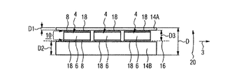
曲げ変換器2の図面に示す様々な変形実施形態は、長手方向3に延在し、それぞれ、少なくとも1つの圧電素子4を有する。圧電素子4は、一般に、圧電材料、特に圧電セラミック6(好ましくはPZTセラミック)から構成される層で構成される。電極層8が圧電セラミック6の両側に編成(配置)されている。電極層8を有する圧電セラミック6は、それぞれ、圧電素子4を形成する。
The various variant embodiments shown in the drawing of the bending transducer 2 extend in the
圧電素子4は、図1A、図1Bおよび図2A、図2Bによる変形実施形態において、同時に層構成10を形成する。図3に示すモノモルフ構成において、層構成10は、機械的キャリア12により形成され、機械的キャリア12の片側に、圧電素子4が編成(配置)されている。図4によるトライモルフ変形実施形態において、層構成10は、機械的キャリア12と、機械的キャリア12の両側に適用された(付けられた)圧電素子4とにより形成されている。機械的キャリア自体は、様々な変形実施形態において基本的に既知であり、例えば絶縁材料から、または例えば金属などの導電性材料から形成されている。導電性素子としての構成において、隣接する(接触する)電極層8は省略してもよい。キャリア12の厚さは、典型的には、圧電素子4の厚さよりも大きく、典型的には、0.2〜3mmの範囲である。これらの異なる層構成10の製造は、それ自体、既知である。
The
図面に示すすべての曲げ変換器2は、特にプレストレス下で層構成10上に適用された(付けられた)、例えば少なくとも1つの弾性保護層14A、Bを追加的に編成(配置)することにより特徴付けられている。これにより、前記保護層は、少なくとも長手方向3の配向(方位)において、結合面内において圧力または剪断荷重を働かせる。このため、プレストレスにより働く力は、外方領域から中心領域に方向付けられている。
All the bending transducers 2 shown in the drawings are additionally knitted (arranged), for example, at least one elastic
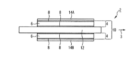
図3によるモノモルフ構成では、1つの保護層14Aのみが層構成10の外側に適用されているが(付けられているが)、その他の変形実施形態では、それぞれ、1つの保護層14A、14Bが層構成10の両方の対向する外側に適用されている(付けられている)。この場合、保護層14A、14Bは、好ましくは、例えばアクリレートまたはエポキシ樹脂系の好適な接着剤を用いて適用される(付けられる)。適切であれば、導電性接着剤を用いてもよい。保護層14A、14Bは、好ましくは、少なくとも一方向において層構成の縁辺に重なるように、層構成10よりも大きい表面積を有する。
In the monomorph configuration according to FIG. 3, only one
一般に、図1A、図1B、図2A、図2B、および図4による変形実施形態は、層構成が2つの膜タイプの保護層の間の(に)サンドイッチの形態で接着結合により編成(配置)されているという点において特徴付けられている。 In general, the variant embodiments according to FIG. 1A, FIG. 1B, FIG. 2A, FIG. 2B and FIG. 4 are knitted (arranged) by adhesive bonding in the form of a sandwich between two membrane-type protective layers. It is characterized in that it is
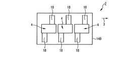
図1A、1Bによる変形実施形態において、連続的な圧電素子は設けられていないが、個々のセグメントが2つの保護層13A、13Bの間の圧電素子4上に編成(配置)されている。
In the variant embodiment according to FIGS. 1A and 1B, continuous piezoelectric elements are not provided, but individual segments are knitted (arranged) on the
図1Aにおいて、曲げ変換器2の中立帯16を点線により追加的に示している。ここで、中立帯16は、個々の層に対して平行に延在する中心面、つまり、2つの保護層14A、14Bの外方の平坦な側により形成された曲げ変換器2の外方の平坦な側から同じ距離を有する中心面により形成されている。図1Aにおいて見られるように、層構成10は、この中立帯に対して非対称的に編成(配置)され、特に、完全に中立帯16の外に移動されている。例示的実施形態において、層構成10は、中立帯16に直接隣接(接触)している。
In FIG. 1A, the
例示的実施形態において、これは、2つの保護層14A、14Bの厚さが異なることにより達成されている。ここで、上側保護層14Aは、下側保護層14Bの厚さD2と比較して相当に小さい厚さD1を有する。例示的実施形態において、厚さD2は、厚さD1と層構成10の厚さD3との合計に等しい。典型的には、1つの圧電セラミック6層のみが用いられるときの層構成10の厚さD3は、例えば50〜約500μmの範囲である。圧電セラミック6の両側に適用される(付けられる)電極層8は、それぞれ、電極層の構成によって変化する可能性がある厚さを有し、例えば金電極が用いられるとき、数100nmである。炭素電極が用いられるとき、電極層の厚さは、例えば5〜50μmである。炭素電極とは、一般に、追加的な埋め込まれた顔料粒子としてグラファイトを有する熱硬化性樹脂(例えばエポキシ樹脂)が適用された炭素重合体から作製された電極を意味するものと理解される。
In the exemplary embodiment, this is achieved by the different thicknesses of the two
保護層14A、14Bは、好ましくは、プリント回路基板材料、例えばFR4材料として既知の材料から形成されている。FR4材料は、ガラス繊維で強化された硬化したエポキシ樹脂である。保護層14A、14Bの厚さは、好ましくは、100μmよりも大きい。例示的実施形態において、例えば、200〜500μmの範囲の厚さD3を有する層構成10と、100〜200μmの範囲の厚さD1を有する上側保護層14Aとが用いられる。すると、下側保護層14Bの厚さD2は、400〜700μmの範囲となる。
The
図1A、図1Bの例示的実施形態において、導体トラック18の形態の導電性領域が保護層14A、14B上に適用されている(付けられている)。保護層14A、14Bは、導体トラック18とともに、膜タイプのフレキシブルプリント回路基板を形成する。保護層14A、14Bは、この場合、前記フレキシブルプリント回路基板のキャリア層であり、かかるキャリア層上に、導体トラック18が適用されている(付けられている)。個々の電極層8の接触は、導体トラック18を介して特に簡単かつ効率的に行われる。このため、機械的変形において生成された電気信号(電荷キャリア)の送信は、プリント回路基板とその導体トラック18とを介して簡単に行うことが可能である。この場合、下流に接続された制御ユニットまたはエネルギー貯蔵への送信のための個々の導体トラック18の接触は、接点(ここではより詳細に図示しない)を介して行われ、かかる接点は、例えば接触トラック18の拡幅された接触面により形成され、かかる接触面上に、例えば接続ワイヤが半田付けなどされる。図1Bによる平面図において、導体トラック18の接続可能性は、図示していない。これらは、外部への導体トラック18(部分的にのみ図示)により概略的にのみ図示している。
In the exemplary embodiment of FIGS. 1A and 1B, a conductive region in the form of a
大きい厚さD2を有する下側保護層14Bの構成について、保護層の個々の膜の複数のプライを互いに重ねるように編成(配置)することも可能である。図1Aに示すような曲げ変換器は、例えば一端側において、例えばその左端において、保持装置においてクランプ固定され、対向する右端は、自由端を形成する。自由端は、個々の圧電素子4が圧力によってのみ荷重されるように、設置状態において、好ましくは矢印20により示す曲げ方向にのみ偏向されている(偏向される)。
Regarding the configuration of the lower
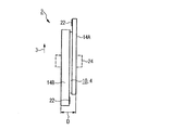
図2A、図2Bによる例示的実施形態は、大部分、図1A、図1Bによる例示的実施形態に対応している。この場合も、曲げ変換器2は、異なる厚さを有する2つの対向する保護層14A、14Bと、保護層14A、14Bの間に編成(配置)された(単一の)圧電素子4とにより形成されている。保護層14A、14Bは、図1Aおよび図1Bの例示的実施形態におけるように、圧電素子4に対して突出している。図2A、図2Bによる変形において、保護層14A、14Bは、2つの保護層14A、14Bが長手方向においてオフセットされて編成(配置)されるとともに互いに対して突出する領域を有するように、曲げ変換器2の長手方向において圧電素子4に対して突出している。これらの突出領域において、接触面22が保護層14A、14Bの内側に形成され、かかる接触面上に、例えば接続ワイヤが半田付けされる。この場合も、好ましくは、保護層14A、14Bに、電極層8(さらなる詳細は図示せず)を接触させるための導体トラック18(やはりさらなる詳細は図示せず)が設けられる。
The exemplary embodiment according to FIGS. 2A and 2B largely corresponds to the exemplary embodiment according to FIGS. 1A and 1B. In this case as well, the bending transducer 2 is constituted by two opposing
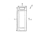
図2Aにおいて、曲げ変換器の領域における概ね中心において、可能性のある装着箇所24が点線により示され、かかる箇所において、曲げ変換器が例えばその装着端位置においてクランプ固定される。図2Bは、装着箇所24を伴わない、図2Aに対して90°回転した図である。曲げ変換器2の幅Bは、一般に典型的には、3〜10mmの範囲であり、例示的実施形態において例えば5.5mmである。典型的な曲げ変換器2の長さLは、例えば20〜50mmの範囲であり、例示的実施形態において例えば約30mmである。典型的な曲げ変換器の全厚Dは、例えば400〜1500μmの範囲であり、図1Aおよび図2Aによる例示的実施形態において約650μmの範囲である。
In FIG. 2A, a possible mounting
図面に示す例示的実施形態において、それぞれ、保護層14A、14Bは、導体トラック18が適用された(付けられた)追加層としての電極層8を有する層構成10の外側に適用されている(付けられている)。1つの代替の変形実施形態において、導電性層が、電極層8を形成する保護層14A、14B上に適用される(付けられる)。
In the exemplary embodiment shown in the drawings, the
すべての例示的実施形態は、保護層14A、14Bの使用により特徴付けられており、好ましくは、層構成10は、2つの保護層14A、14Bの間に接着結合により編成(配置)されている。この方策により、層構成の荷重容量が著しく増加し、破損のリスクが低減される。この方策により、全体として、曲げ変換器2の相当に高い曲げ応力が可能になる。
All exemplary embodiments are characterized by the use of
さらなる特別な設計上の特長としては、発電機の動作についてかなりのエネルギー生成を可能にするために、圧電層構成(圧電活性層構造)10を曲げ変換器2の中立帯16の外に移動させることが考えられる。さらにその上、特に圧電セラミック6上に編成(配置)された電極層8を補うために、導体トラック18または導電性層を保護層14A、14B上に直接編成(配置)することを強調すべきである。これは、導体トラック18により、電極層8を特に簡単な接触させることが可能になるためである。これにより、全体として、簡単に実現可能な接触を有するとともに高い曲げ応力においても確実に機能する、高い荷重容量を有する曲げ変換器2が形成される。特に、保護層14A、14B上に適用された(付けられた)導電性層自体が電極層を形成する(または電極8に加えて設けられる)構成において、特にロバストな接触が可能になる。これは、圧電セラミック6が裂ける可能性がある場合も、圧電セラミック6は、圧電セラミック6の表面の一部が非接触状態で残ることなく、依然として確実に全面積に亘り接触しているためである。導体トラック18または導電性層は、例えば銀、金、炭素、または銅などの導電性材料でスパッタリング、印刷、または積層することにより製造される。
A further special design feature is that the piezoelectric layer configuration (piezoactive layer structure) 10 is moved out of the
2 曲げ変換器
3 長手方向
4 圧電素子
6 圧電セラミック
8 電極層
10 層構成
12 機械的キャリア
14A、B 保護層
16 中立帯
18 導体トラック
20 曲げ方向
22 接触面(コンタクト面)
24 装着箇所
B 幅
D1 厚さ
D2 厚さ
D3 厚さ
L 長さ
2
24 Installation location B Width D1 Thickness D2 Thickness D3 Thickness L Length
Claims (15)
前記2つの膜は、前記層構成(10)上で重なるとともに、それぞれ、前記層構成(10)に面する内側に導体トラック(18)を有し、かかる導体トラック(18)を介して前記圧電素子(4)は前記保護層(14A、14B)に接触するとともに、かかる導体トラック(18)は接触面(22)につながり、かかる接触面(22)は突出する部分的な領域において配置されるとともに、かかる接触面(22)上には、接続状態において接続線が接触し、
前記保護層(14A、14B)は、弾性を有し、弾性復元力がプレストレスを働かせるように、伸張された状態で前記層構成(10)上に適用されている、曲げ変換器(10)。 In a bending transducer (2) having a layer structure (10) comprising a piezoelectric element (4) composed of a piezoelectric material (6) and an electrode layer (8) applied on the piezoelectric material (6). The layer structure (10) has a protective layer (14A, 14B) on the outside, and the layer structure (10) is knitted in the form of a sandwich between two films forming the protective layer (14A, 14B). And
The two films overlap on the layer structure (10), and each has a conductor track (18) on the inner side facing the layer structure (10), and the piezoelectric film is interposed via the conductor track (18). The element (4) contacts the protective layer (14A, 14B), and the conductor track (18) is connected to the contact surface (22), and the contact surface (22) is arranged in a protruding partial region. At the same time, on the contact surface (22), the connection line contacts in the connected state,
The protective layer (14A, 14B) are resilient, to exert an elastic restoring force Gapu Restless, in Shin Zhang state is applied over the layer structure (10), bending transformation Vessel (10).
Applications Claiming Priority (3)
| Application Number | Priority Date | Filing Date | Title |
|---|---|---|---|
| DE102010011047.7 | 2010-03-11 | ||
| DE102010011047A DE102010011047A1 (en) | 2010-03-11 | 2010-03-11 | bending transducer |
| PCT/EP2011/001191 WO2011110353A1 (en) | 2010-03-11 | 2011-03-10 | Bending transducer |
Publications (2)
| Publication Number | Publication Date |
|---|---|
| JP2013522865A JP2013522865A (en) | 2013-06-13 |
| JP5954792B2 true JP5954792B2 (en) | 2016-07-20 |
Family
ID=44123418
Family Applications (1)
| Application Number | Title | Priority Date | Filing Date |
|---|---|---|---|
| JP2012556417A Expired - Fee Related JP5954792B2 (en) | 2010-03-11 | 2011-03-10 | Bending transducer |
Country Status (7)
| Country | Link |
|---|---|
| US (1) | US20130002095A1 (en) |
| EP (1) | EP2545598B1 (en) |
| JP (1) | JP5954792B2 (en) |
| CN (1) | CN102782893B (en) |
| DE (1) | DE102010011047A1 (en) |
| DK (1) | DK2545598T3 (en) |
| WO (1) | WO2011110353A1 (en) |
Families Citing this family (29)
| Publication number | Priority date | Publication date | Assignee | Title |
|---|---|---|---|---|
| KR101725115B1 (en) * | 2010-12-16 | 2017-04-26 | 한국전자통신연구원 | Power Supplier Using a Flexible PCB Based Self-powering and Sensor Node Using The Same |
| DE102011087844A1 (en) * | 2011-12-06 | 2013-06-06 | Johnson Matthey Catalysts (Germany) Gmbh | Assembly for power generation and a bending transducer for such an assembly |
| JP6002524B2 (en) * | 2012-09-28 | 2016-10-05 | 住友理工株式会社 | Transducer |
| DE102013211596A1 (en) | 2013-06-20 | 2014-12-24 | Robert Bosch Gmbh | Method for electrically contacting a piezoceramic |
| EP3049034B1 (en) | 2013-09-29 | 2017-10-25 | Institut Hospitalo-Universitaire de Chirurgie Mini -Invasive Guidee Par l'Image | Implantable device to treat obesity |
| JP6343144B2 (en) * | 2013-12-20 | 2018-06-13 | Jr東日本コンサルタンツ株式会社 | Floor power generation structure |
| DE102014214753A1 (en) * | 2014-07-28 | 2016-01-28 | Robert Bosch Gmbh | Pressure sensor and method of manufacturing a pressure sensor |
| CN113230021A (en) | 2015-01-12 | 2021-08-10 | 科达莱昂治疗公司 | Droplet delivery apparatus and method |
| CN105865670B (en) * | 2015-02-09 | 2020-09-25 | 精工爱普生株式会社 | Force detection device and robot |
| DE102015215942A1 (en) * | 2015-08-20 | 2017-02-23 | Robert Bosch Gmbh | Electronic assembly, in particular for a transmission control module |
| JP6726508B2 (en) * | 2016-04-07 | 2020-07-22 | 日本特殊陶業株式会社 | Piezoelectric actuator |
| CN107819410B (en) * | 2016-09-13 | 2020-11-13 | 广东顺德中山大学卡内基梅隆大学国际联合研究院 | Piezoelectric energy harvester |
| CN109906120A (en) * | 2017-01-20 | 2019-06-18 | 科达莱昂治疗公司 | Piezoelectric fluid distributor |
| WO2018179589A1 (en) * | 2017-03-30 | 2018-10-04 | 三菱電機株式会社 | Optical scanning device and method of manufacture therefor |
| JP7056669B2 (en) * | 2017-11-09 | 2022-04-19 | 株式会社村田製作所 | Piezoelectric components, sensors and actuators |
| WO2019113483A1 (en) | 2017-12-08 | 2019-06-13 | Kedalion Therapeutics, Inc. | Fluid delivery alignment system |
| WO2019197942A1 (en) * | 2018-04-09 | 2019-10-17 | King Abdullah University Of Science And Technology | Energy producing device with a piezoelectric energy generating beam |
| US12350194B1 (en) | 2018-04-12 | 2025-07-08 | Bausch + Lomb Ireland Limited | Topical ocular delivery of fluids with controlled mass dosing and wireless communication |
| US20190314197A1 (en) | 2018-04-12 | 2019-10-17 | Kedalion Therapeutics, Inc. | Topical Ocular Delivery Methods and Devices for Use in the Same |
| WO2020010116A1 (en) | 2018-07-03 | 2020-01-09 | Kedalion Therapeutics, Inc. | Topical ocular delivery devices and methods for using the same |
| US11679028B2 (en) | 2019-03-06 | 2023-06-20 | Novartis Ag | Multi-dose ocular fluid delivery system |
| US12097145B2 (en) | 2019-03-06 | 2024-09-24 | Bausch + Lomb Ireland Limited | Vented multi-dose ocular fluid delivery system |
| US12496218B1 (en) | 2019-11-12 | 2025-12-16 | Bausch + Lomb Ireland Limited | Fractionated topical ocular drug delivery methods and devices for use in the same |
| DE102020107028B4 (en) | 2020-03-13 | 2022-12-29 | Technische Universität Chemnitz | Piezoelectric device and method of making same |
| EP4120973A4 (en) | 2020-04-17 | 2024-04-17 | Bausch + Lomb Ireland Limited | HYDRODYNAMIC ACTUATED PRESERVATIVE-FREE DISPENSING SYSTEM WITH COLLAPSIBLE LIQUID CONTAINER |
| US12290472B2 (en) | 2020-04-17 | 2025-05-06 | Bausch + Lomb Ireland Limited | Hydrodynamically actuated preservative free dispensing system |
| CN115768384A (en) | 2020-04-17 | 2023-03-07 | 科达隆治疗公司 | Hydrodynamically actuated, preservative-free dispensing system |
| US11938057B2 (en) | 2020-04-17 | 2024-03-26 | Bausch + Lomb Ireland Limited | Hydrodynamically actuated preservative free dispensing system |
| US20240206340A1 (en) * | 2021-03-31 | 2024-06-20 | Tdk Corporation | Power generator and power generation system |
Family Cites Families (23)
| Publication number | Priority date | Publication date | Assignee | Title |
|---|---|---|---|---|
| DE3310589A1 (en) | 1983-03-23 | 1984-09-27 | Siemens AG, 1000 Berlin und 8000 München | SYNTHETIC RESIN IMPREGNATED PIEZOCERAMIC BODY |
| EP1088352A1 (en) * | 1998-05-29 | 2001-04-04 | Motorola, Inc. | Resonant piezoelectric alerting device |
| DE19856202A1 (en) * | 1998-12-05 | 2000-06-15 | Bosch Gmbh Robert | Piezoelectric actuator |
| US6512323B2 (en) * | 2000-03-22 | 2003-01-28 | Caterpillar Inc. | Piezoelectric actuator device |
| JP2001354497A (en) * | 2000-06-07 | 2001-12-25 | Matsushita Electric Ind Co Ltd | Manufacturing method of ferroelectric film |
| EP1168463A1 (en) * | 2000-06-23 | 2002-01-02 | DORNIER GmbH | Fiber composite with integrated piezoelectric actor or sensor |
| US6515402B2 (en) * | 2001-01-24 | 2003-02-04 | Koninklijke Philips Electronics N.V. | Array of ultrasound transducers |
| US20020140321A1 (en) * | 2001-03-27 | 2002-10-03 | Waterfield Larry G. | Coated electroactive bender actuator |
| US20040021529A1 (en) * | 2002-07-30 | 2004-02-05 | Bradley Paul D. | Resonator with protective layer |
| US6965189B2 (en) * | 2002-09-20 | 2005-11-15 | Monodrive Inc. | Bending actuators and sensors constructed from shaped active materials and methods for making the same |
| US20050012434A1 (en) * | 2003-03-26 | 2005-01-20 | Continuum Photonics, Inc. | Robust piezoelectric power generation module |
| US20050210988A1 (en) * | 2004-03-05 | 2005-09-29 | Jun Amano | Method of making piezoelectric cantilever pressure sensor array |
| DE102004046150A1 (en) * | 2004-09-23 | 2006-03-30 | Fraunhofer-Gesellschaft zur Förderung der angewandten Forschung e.V. | Device and method for influencing the vibration of a surface element |
| DE102005020527A1 (en) * | 2005-05-03 | 2006-11-09 | Festo Ag & Co. | Piezoelectric unit for use as e.g. print head for ink jet printer, has supporting body electrically contacted by piezoelectric inactive material, which is glass fiber reinforced plastic overlying in contacting region of body |
| DE102005055870A1 (en) * | 2005-11-23 | 2007-05-24 | Epcos Ag | Electroacoustic component, has layer system arranged between carrier substrate and piezo substrate, and comprising metal layer and dielectric layer, where thickness of piezo substrate is maximally half of thickness of carrier substrate |
| JP2007167998A (en) * | 2005-12-20 | 2007-07-05 | Toshiba Corp | Device having beam structure and semiconductor device |
| US20070188053A1 (en) * | 2006-02-14 | 2007-08-16 | Robert Bosch Gmbh | Injection molded energy harvesting device |
| JP2007273589A (en) * | 2006-03-30 | 2007-10-18 | Fujitsu Ltd | Thin film piezoelectric device and manufacturing method thereof |
| JP2007316045A (en) * | 2006-04-25 | 2007-12-06 | Matsushita Electric Ind Co Ltd | Pressure detection element |
| US7414351B2 (en) * | 2006-10-02 | 2008-08-19 | Robert Bosch Gmbh | Energy harvesting device manufactured by print forming processes |
| JP2008301453A (en) * | 2007-06-04 | 2008-12-11 | Toshiba Corp | Thin film piezoelectric resonator and filter circuit using the same |
| DE102008007774A1 (en) | 2008-02-06 | 2009-08-13 | Robert Bosch Gmbh | Bending transducer for generating electrical energy from mechanical deformations |
| WO2010008381A1 (en) * | 2008-07-15 | 2010-01-21 | Iptrade, Inc. | Unimorph/bimorph piezoelectric package |
-
2010
- 2010-03-11 DE DE102010011047A patent/DE102010011047A1/en not_active Ceased
-
2011
- 2011-03-10 EP EP11713177.1A patent/EP2545598B1/en not_active Not-in-force
- 2011-03-10 JP JP2012556417A patent/JP5954792B2/en not_active Expired - Fee Related
- 2011-03-10 CN CN201180011884.5A patent/CN102782893B/en not_active Expired - Fee Related
- 2011-03-10 US US13/583,997 patent/US20130002095A1/en not_active Abandoned
- 2011-03-10 WO PCT/EP2011/001191 patent/WO2011110353A1/en not_active Ceased
- 2011-03-10 DK DK11713177.1T patent/DK2545598T3/en active
Also Published As
| Publication number | Publication date |
|---|---|
| EP2545598B1 (en) | 2014-02-26 |
| US20130002095A1 (en) | 2013-01-03 |
| EP2545598A1 (en) | 2013-01-16 |
| DK2545598T3 (en) | 2014-05-05 |
| DE102010011047A1 (en) | 2011-09-15 |
| CN102782893A (en) | 2012-11-14 |
| JP2013522865A (en) | 2013-06-13 |
| CN102782893B (en) | 2015-10-07 |
| WO2011110353A1 (en) | 2011-09-15 |
Similar Documents
| Publication | Publication Date | Title |
|---|---|---|
| JP5954792B2 (en) | Bending transducer | |
| JP3524557B2 (en) | Piezoelectric flexural transducer and method of manufacturing the same | |
| JP5318761B2 (en) | Piezoelectric ceramic planar actuator and method of manufacturing the planar actuator | |
| JP4785434B2 (en) | Piezoelectric ceramic fiber with metal core | |
| JP2008122215A (en) | Piezoelectric sensor and manufacturing method thereof | |
| JP5111071B2 (en) | Piezoelectric sensor | |
| US6316865B1 (en) | Piezoelectric element | |
| KR101578806B1 (en) | Flexible piezo-electric loudspeaker including battery | |
| KR101467933B1 (en) | Piezo fiber composite structure and device using thereof | |
| US20080211353A1 (en) | High temperature bimorph actuator | |
| KR20230010710A (en) | piezoelectric element | |
| US20020084720A1 (en) | Piezoelectric bending transducer | |
| KR101612456B1 (en) | Piezo-electric fiber composite structure and piezo-electric film speaker using thereof | |
| KR102381748B1 (en) | Multilayer transformable device and display device comprising the same | |
| US7105988B2 (en) | Piezoelectric device and method to manufacture a piezoelectric device | |
| JP2004266643A (en) | Piezoelectric sounding element and method of manufacturing the same | |
| KR101594432B1 (en) | Electrostatic force based actuator including poly-imide organic dielectric layer | |
| US20040012308A1 (en) | Piezo-electric bending transducer | |
| US6313401B1 (en) | Thermally stable actuator/sensor structure | |
| KR20220076506A (en) | piezoelectric element | |
| CN104538545B (en) | Ferroelastic domain switching based large actuating strain piezoelectric actuator | |
| JP4673418B2 (en) | Vibrating transfer device | |
| JP6882096B2 (en) | Piezoelectric power generator | |
| KR101467934B1 (en) | Piezo fiber composite structure and device using thereof | |
| KR101577961B1 (en) | Piezo fiber composite structure |
Legal Events
| Date | Code | Title | Description |
|---|---|---|---|
| RD03 | Notification of appointment of power of attorney |
Free format text: JAPANESE INTERMEDIATE CODE: A7423 Effective date: 20140203 |
|
| RD04 | Notification of resignation of power of attorney |
Free format text: JAPANESE INTERMEDIATE CODE: A7424 Effective date: 20140205 |
|
| A621 | Written request for application examination |
Free format text: JAPANESE INTERMEDIATE CODE: A621 Effective date: 20140207 |
|
| A131 | Notification of reasons for refusal |
Free format text: JAPANESE INTERMEDIATE CODE: A131 Effective date: 20150113 |
|
| A977 | Report on retrieval |
Free format text: JAPANESE INTERMEDIATE CODE: A971007 Effective date: 20150115 |
|
| A601 | Written request for extension of time |
Free format text: JAPANESE INTERMEDIATE CODE: A601 Effective date: 20150410 |
|
| A601 | Written request for extension of time |
Free format text: JAPANESE INTERMEDIATE CODE: A601 Effective date: 20150612 |
|
| A521 | Request for written amendment filed |
Free format text: JAPANESE INTERMEDIATE CODE: A523 Effective date: 20150713 |
|
| A131 | Notification of reasons for refusal |
Free format text: JAPANESE INTERMEDIATE CODE: A131 Effective date: 20151020 |
|
| A521 | Request for written amendment filed |
Free format text: JAPANESE INTERMEDIATE CODE: A523 Effective date: 20160105 |
|
| TRDD | Decision of grant or rejection written | ||
| A01 | Written decision to grant a patent or to grant a registration (utility model) |
Free format text: JAPANESE INTERMEDIATE CODE: A01 Effective date: 20160510 |
|
| A61 | First payment of annual fees (during grant procedure) |
Free format text: JAPANESE INTERMEDIATE CODE: A61 Effective date: 20160608 |
|
| R150 | Certificate of patent or registration of utility model |
Ref document number: 5954792 Country of ref document: JP Free format text: JAPANESE INTERMEDIATE CODE: R150 |
|
| LAPS | Cancellation because of no payment of annual fees |