JP5947534B2 - Contactless power supply system - Google Patents
Contactless power supply system Download PDFInfo
- Publication number
- JP5947534B2 JP5947534B2 JP2011277792A JP2011277792A JP5947534B2 JP 5947534 B2 JP5947534 B2 JP 5947534B2 JP 2011277792 A JP2011277792 A JP 2011277792A JP 2011277792 A JP2011277792 A JP 2011277792A JP 5947534 B2 JP5947534 B2 JP 5947534B2
- Authority
- JP
- Japan
- Prior art keywords
- power
- matching circuit
- circuit
- resonance coil
- power feeding
- Prior art date
- Legal status (The legal status is an assumption and is not a legal conclusion. Google has not performed a legal analysis and makes no representation as to the accuracy of the status listed.)
- Expired - Fee Related
Links
- 230000005540 biological transmission Effects 0.000 claims description 67
- 238000000034 method Methods 0.000 description 12
- 238000010586 diagram Methods 0.000 description 8
- HEZMWWAKWCSUCB-PHDIDXHHSA-N (3R,4R)-3,4-dihydroxycyclohexa-1,5-diene-1-carboxylic acid Chemical compound O[C@@H]1C=CC(C(O)=O)=C[C@H]1O HEZMWWAKWCSUCB-PHDIDXHHSA-N 0.000 description 7
- 238000009774 resonance method Methods 0.000 description 7
- 239000003990 capacitor Substances 0.000 description 5
- 230000001413 cellular effect Effects 0.000 description 5
- 238000006243 chemical reaction Methods 0.000 description 5
- 238000010168 coupling process Methods 0.000 description 4
- 230000008878 coupling Effects 0.000 description 2
- 238000005859 coupling reaction Methods 0.000 description 2
- 230000003071 parasitic effect Effects 0.000 description 2
- 230000005611 electricity Effects 0.000 description 1
- 230000005674 electromagnetic induction Effects 0.000 description 1
- 230000002250 progressing effect Effects 0.000 description 1
- 238000012827 research and development Methods 0.000 description 1
Images


Classifications
-
- H—ELECTRICITY
- H02—GENERATION; CONVERSION OR DISTRIBUTION OF ELECTRIC POWER
- H02J—CIRCUIT ARRANGEMENTS OR SYSTEMS FOR SUPPLYING OR DISTRIBUTING ELECTRIC POWER; SYSTEMS FOR STORING ELECTRIC ENERGY
- H02J7/00—Circuit arrangements for charging or depolarising batteries or for supplying loads from batteries
- H02J7/00032—Circuit arrangements for charging or depolarising batteries or for supplying loads from batteries characterised by data exchange
- H02J7/00034—Charger exchanging data with an electronic device, i.e. telephone, whose internal battery is under charge
-
- H—ELECTRICITY
- H02—GENERATION; CONVERSION OR DISTRIBUTION OF ELECTRIC POWER
- H02J—CIRCUIT ARRANGEMENTS OR SYSTEMS FOR SUPPLYING OR DISTRIBUTING ELECTRIC POWER; SYSTEMS FOR STORING ELECTRIC ENERGY
- H02J50/00—Circuit arrangements or systems for wireless supply or distribution of electric power
- H02J50/10—Circuit arrangements or systems for wireless supply or distribution of electric power using inductive coupling
- H02J50/12—Circuit arrangements or systems for wireless supply or distribution of electric power using inductive coupling of the resonant type
-
- H—ELECTRICITY
- H01—ELECTRIC ELEMENTS
- H01F—MAGNETS; INDUCTANCES; TRANSFORMERS; SELECTION OF MATERIALS FOR THEIR MAGNETIC PROPERTIES
- H01F38/00—Adaptations of transformers or inductances for specific applications or functions
- H01F38/14—Inductive couplings
-
- H—ELECTRICITY
- H02—GENERATION; CONVERSION OR DISTRIBUTION OF ELECTRIC POWER
- H02J—CIRCUIT ARRANGEMENTS OR SYSTEMS FOR SUPPLYING OR DISTRIBUTING ELECTRIC POWER; SYSTEMS FOR STORING ELECTRIC ENERGY
- H02J50/00—Circuit arrangements or systems for wireless supply or distribution of electric power
- H02J50/005—Mechanical details of housing or structure aiming to accommodate the power transfer means, e.g. mechanical integration of coils, antennas or transducers into emitting or receiving devices
-
- H—ELECTRICITY
- H02—GENERATION; CONVERSION OR DISTRIBUTION OF ELECTRIC POWER
- H02J—CIRCUIT ARRANGEMENTS OR SYSTEMS FOR SUPPLYING OR DISTRIBUTING ELECTRIC POWER; SYSTEMS FOR STORING ELECTRIC ENERGY
- H02J50/00—Circuit arrangements or systems for wireless supply or distribution of electric power
- H02J50/40—Circuit arrangements or systems for wireless supply or distribution of electric power using two or more transmitting or receiving devices
-
- H—ELECTRICITY
- H02—GENERATION; CONVERSION OR DISTRIBUTION OF ELECTRIC POWER
- H02J—CIRCUIT ARRANGEMENTS OR SYSTEMS FOR SUPPLYING OR DISTRIBUTING ELECTRIC POWER; SYSTEMS FOR STORING ELECTRIC ENERGY
- H02J50/00—Circuit arrangements or systems for wireless supply or distribution of electric power
- H02J50/80—Circuit arrangements or systems for wireless supply or distribution of electric power involving the exchange of data, concerning supply or distribution of electric power, between transmitting devices and receiving devices
-
- H—ELECTRICITY
- H02—GENERATION; CONVERSION OR DISTRIBUTION OF ELECTRIC POWER
- H02J—CIRCUIT ARRANGEMENTS OR SYSTEMS FOR SUPPLYING OR DISTRIBUTING ELECTRIC POWER; SYSTEMS FOR STORING ELECTRIC ENERGY
- H02J50/00—Circuit arrangements or systems for wireless supply or distribution of electric power
- H02J50/90—Circuit arrangements or systems for wireless supply or distribution of electric power involving detection or optimisation of position, e.g. alignment
Description
本発明は給電装置、及び当該給電装置を具備する非接触給電システムに関する。 The present invention relates to a power feeding device and a non-contact power feeding system including the power feeding device.
様々な電子機器の普及が進み、多種多様な製品が市場に出荷されている。近年では、携帯電話及びデジタルビデオカメラ等の携帯型の電子機器の普及が顕著である。また電力を基に動力を得る電気自動車等の電気推進移動体も製品として市場に登場しつつある。 Various electronic devices are spreading and various products are shipped to the market. In recent years, portable electronic devices such as mobile phones and digital video cameras have been widely used. In addition, electric propulsion vehicles such as electric vehicles that obtain power based on electric power are also appearing on the market as products.
携帯電話、デジタルビデオカメラまたは電気推進移動体には、蓄電手段であるバッテリーが内蔵されている。当該バッテリーの充電は、殆どが給電手段である家庭用交流電源より直接接触させて行われているのが現状である。またバッテリーを具備しない構成またはバッテリーに充電された電力を用いない構成では、家庭用交流電源より配線等を介して直接給電し動作させているのが現状である。 A mobile phone, a digital video camera, or an electric propulsion mobile body has a built-in battery as a power storage means. At present, most of the battery is charged by direct contact with a household AC power source as a power supply means. Further, in a configuration without a battery or a configuration in which no electric power charged in the battery is used, the current situation is that power is directly supplied from a household AC power supply via wiring or the like.
一方で非接触によりバッテリーの充電または負荷への給電を行う方式についての研究開発も進んでおり、代表的な方式として、電磁結合方式(電磁誘導方式ともいう)、電波方式(マイクロ波方式ともいう)、共鳴方式が挙げられる。電磁結合方式については、小型家電機器等、普及が進んでいる電子機器もある。 On the other hand, research and development on a method for charging a battery or supplying power to a load in a non-contact manner is also progressing. Typical methods include an electromagnetic coupling method (also referred to as an electromagnetic induction method) and a radio wave method (also referred to as a microwave method). ), Resonance method. As for the electromagnetic coupling method, there are some electronic devices that are widely used, such as small home appliances.
また、共鳴方式の非接触給電システムとしては、特許文献1又は2にあるように電力の伝送効率(送電効率)の向上を図るべく、開発が進んでいる。
Further, as described in
共鳴方式による非接触給電システムでは、電力を受ける側の装置(以下、受電装置)が有する共鳴用コイルと、電力を供給する側の装置(以下、給電装置)が有する共鳴用コイルとの距離によって、効率が高い送電が可能な条件が異なってしまい、安定して効率の高い送電を行うことが困難である。 In a non-contact power feeding system using a resonance method, the distance between a resonance coil included in a device that receives power (hereinafter referred to as a power receiving device) and a resonance coil included in a device that supplies power (hereinafter referred to as a power feeding device). The conditions under which high-efficiency power transmission is possible differ, making it difficult to perform stable and efficient power transmission.
また、給電時に受電装置と給電装置の配置が変化すると、送電の効率が低下してしまうおそれがある。 In addition, if the arrangement of the power receiving device and the power feeding device changes during power feeding, the power transmission efficiency may be reduced.
そこで、本発明の一態様は、電力の伝送効率を高めることができる共鳴方式による給電システムを提供することを目的とする。 In view of the above, an object of one embodiment of the present invention is to provide a power feeding system using a resonance method that can increase power transmission efficiency.
本発明の一態様は、高周波電源に第1の整合回路を介して接続された第1の共鳴用コイルと、第1の整合回路及び第1の送受信回路にそれぞれ接続された第1の制御回路と、を有する給電装置と、第1の共鳴用コイルと電磁共鳴をする第2の共鳴用コイルと、負荷、第2の整合回路、及び第2の送受信回路にそれぞれ接続された第2の制御回路と、を有する受電装置と、を有する非接触給電システムである。 One embodiment of the present invention includes a first resonance coil connected to a high-frequency power source via a first matching circuit, and a first control circuit connected to each of the first matching circuit and the first transmission / reception circuit. And a second control coil connected to a load, a second matching circuit, and a second transmission / reception circuit, respectively, and a second control coil that performs electromagnetic resonance with the first resonance coil. And a power receiving device having a circuit.
上記構成において、第1の整合回路及び第2の整合回路は、回路構成が同じである、非接触給電システムである。 In the above configuration, the first matching circuit and the second matching circuit are contactless power supply systems having the same circuit configuration.
上記構成において、第1の整合回路は、高周波電源と直列に接続された第1の素子と、高周波電源と並列に接続された第2の素子とを有し、第2の整合回路は、負荷と直列に接続された第3の素子と、負荷と並列に接続された第4の素子と、を有する、非接触給電システムである。 In the above configuration, the first matching circuit includes a first element connected in series with the high-frequency power source and a second element connected in parallel with the high-frequency power source, and the second matching circuit includes a load And a fourth element connected in parallel with the load. The non-contact power feeding system.
上記構成において、第1の素子と第3の素子とは、同じ構成を有する素子であり、第2の素子と第4の素子とは、同じ構成を有する素子である、非接触給電システムである。 In the above structure, the first element and the third element are elements having the same structure, and the second element and the fourth element are elements having the same structure, which is a non-contact power feeding system. .
上記構成において、第1の素子及び第3の素子は、可変容量素子であり、第2の素子及び第4の素子は、可変コイルである、非接触給電システムである。 In the above structure, the first element and the third element are variable capacitance elements, and the second element and the fourth element are a variable coil, which is a non-contact power feeding system.
本発明の一態様は、高周波電源に接続された第1のコイルと、第1のコイルと電磁結合をする第1の共鳴用コイルと、第1の共鳴用コイルに接続された第1の整合回路と、第1の整合回路と第1の送受信回路にそれぞれ接続された第1の制御回路と、を有する給電装置と、第1の共鳴用コイルと電磁共鳴をする第2の共鳴用コイルと、第2の共鳴用コイルに接続された第2の整合回路と、第2の共鳴用コイルと電磁結合をし、第2の整流回路を介して負荷に接続された第2のコイルと、負荷、第2の整合回路、及び第2の送受信回路にそれぞれ接続された第2の制御回路と、を有する受電装置と、を有する非接触給電システムである。 One aspect of the present invention includes a first coil connected to a high-frequency power source, a first resonance coil that is electromagnetically coupled to the first coil, and a first matching connected to the first resonance coil. A power supply device including a circuit, a first matching circuit, and a first control circuit connected to the first transmission / reception circuit, a second resonance coil that performs electromagnetic resonance with the first resonance coil, and A second matching circuit connected to the second resonance coil, a second coil electromagnetically coupled to the second resonance coil, and connected to the load via the second rectifier circuit; , A second matching circuit, and a second control circuit connected to the second transmission / reception circuit, respectively, and a power receiving device.
本発明の一態様は、高周波電源に第1の整合回路を介して接続された第1のコイルと、第1のコイルと電磁結合する第1の共鳴用コイルと、第1の整合回路及び第1の送受信回路にそれぞれ接続された第1の制御回路と、を有する給電装置と、第1の共鳴用コイルと電磁共鳴をする第2の共鳴用コイルと、第2の共鳴用コイルと電磁結合をし、第2の整合回路及び整流回路を介して負荷に接続された第2のコイルと、負荷、第2の整合回路、及び第2の送受信回路にそれぞれ接続された第2の制御回路と、を有する受電装置と、を有する非接触給電システムである。 One embodiment of the present invention includes a first coil connected to a high-frequency power source through a first matching circuit, a first resonance coil that is electromagnetically coupled to the first coil, a first matching circuit, and a first matching circuit. A first control circuit connected to each of the transmission / reception circuits, a second resonance coil that performs electromagnetic resonance with the first resonance coil, and an electromagnetic coupling with the second resonance coil A second coil connected to the load via the second matching circuit and the rectifier circuit, and a second control circuit connected to the load, the second matching circuit, and the second transmission / reception circuit, respectively. , A non-contact power feeding system having a power receiving device.
上記構成において、第1の整合回路及び第2の整合回路は、回路構成が同じである、非接触給電システムである。 In the above configuration, the first matching circuit and the second matching circuit are contactless power supply systems having the same circuit configuration.
上記構成において、第1の整合回路は、第1の共鳴用コイルと接続された第5の素子を有し、第2の整合回路は、第2の共鳴用コイルと接続された第6の素子を有する、非接触給電システムである。 In the above configuration, the first matching circuit has a fifth element connected to the first resonance coil, and the second matching circuit has a sixth element connected to the second resonance coil. It is a non-contact electric power feeding system which has.
上記構成において、第5の素子及び第6の素子は、可変容量素子である、非接触給電システムである。 In the above structure, the fifth element and the sixth element are non-contact power feeding systems which are variable capacitance elements.
本発明の一態様は、給電時に受電装置と給電装置の配置に応じて、電力の伝送効率を高めることができる共鳴方式による非接触給電システムを提供することができる。これにより、給電装置は、受電装置へ電力を効率よく供給することができる。このため、給電利用者にとって、より利便性が高い給電システムを提供することができる。 One embodiment of the present invention can provide a contactless power supply system using a resonance method that can increase power transmission efficiency in accordance with the arrangement of a power reception device and a power supply device during power supply. Thereby, the power feeding device can efficiently supply power to the power receiving device. For this reason, it is possible to provide a power supply system that is more convenient for power supply users.
以下、本発明の実施の形態について図面を参照しながら説明する。但し、本発明は多くの異なる態様で実施することが可能であり、本発明の趣旨及びその範囲から逸脱することなくその形態及び詳細を様々に変更し得ることは当業者であれば容易に理解される。従って実施の形態の記載内容に限定して解釈されるものではない。なお、以下に説明する発明の構成において、同じ物を指し示す符号は異なる図面間において共通とする。 Hereinafter, embodiments of the present invention will be described with reference to the drawings. However, the present invention can be implemented in many different modes, and those skilled in the art can easily understand that the modes and details can be variously changed without departing from the spirit and scope of the present invention. Is done. Therefore, the present invention is not construed as being limited to the description of the embodiments. Note that in the structures of the invention described below, the same portions are denoted by the same reference numerals in different drawings.
なお、各実施の形態の図面等において示す各構成の大きさ、層の厚さ、信号波形は、明瞭化のために誇張されて表記している場合がある。よって、必ずしもそのスケールに限定されない。 Note that the size, layer thickness, and signal waveform of each component illustrated in the drawings and the like in the embodiments are exaggerated for simplicity in some cases. Therefore, it is not necessarily limited to the scale.
なお本明細書にて用いる第1乃至第n(nは自然数)という用語は、構成要素の混同を避けるために付したものであり、数的に限定するものではないことを付記する。
It should be noted that the
(実施の形態1)
本実施の形態では、本発明の一態様における共鳴方式による非接触給電を行う非接触給電システムについて説明する。
(Embodiment 1)
In this embodiment, a contactless power feeding system that performs contactless power feeding by a resonance method according to one embodiment of the present invention will be described.
〈非接触給電システムの構成〉
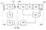
図1に、本発明の一態様に係る非接触給電システムの構成について示す。図1に示す非接触給電システムでは、共鳴方式が適用されている。図1に示す非接触給電システムは、給電装置110及び受電装置120を含むように構成される。図1では、給電装置110における第1の共鳴用コイル112と、受電装置120における第2の共鳴用コイル122とが共鳴することで、電磁波による送電を行うことができる。
<Configuration of wireless power supply system>
FIG. 1 illustrates a structure of a contactless power feeding system according to one embodiment of the present invention. In the non-contact power feeding system shown in FIG. 1, a resonance method is applied. The non-contact power feeding system illustrated in FIG. 1 is configured to include a
給電装置110は、高周波電源111と、第1の共鳴用コイル112と、第1の整合回路113と、第1の制御回路114と、第1の送受信回路115と、第1のアンテナ116とを有する。給電装置110において、高周波電源111は、第1の整合回路113を介して第1の共鳴用コイル112と接続され、第1の整合回路113は、第1の制御回路114を介して第1の送受信回路115と接続されている。
The
また、受電装置120は、負荷121と、第2の共鳴用コイル122と、第2の整合回路123と、第2の制御回路124と、第2の送受信回路125と、第2のアンテナ126と、整流回路127と、DCDCコンバータ128とを有する。受電装置120において、第2の共鳴用コイル122は、第2の整合回路123、整流回路127、及びDCDCコンバータ128を介して負荷121と接続されており、負荷121は、第2の制御回路124を介して第2の整合回路123、第2の送受信回路125にそれぞれ接続されている。なお、DCDCコンバータは、負荷121の中に組み込まれていてもよい。
The
なお、図示しないが、受電装置120において、負荷121と第2の制御回路124との間に、A/D変換回路を設けてもよいし、第2の制御回路124と第2の整合回路123との間にD/A変換回路を設けてもよい。また、給電装置110において、第1の制御回路114と第1の整合回路113との間にD/A変換回路を設けてもよい。また、第2の制御回路124は、A/D変換回路を含む構成としてもよい。
Although not illustrated, in the
給電装置110が有する第1の整合回路113は、高周波電源111と直列に接続された少なくとも一つの素子と、高周波電源111と並列に接続された少なくとも一つの素子とを有する。また、受電装置120が有する第2の整合回路123は、負荷121と直列に接続された少なくとも一つの素子と、負荷121に並列に接続された少なくとも一つの素子とを有する。なお、本明細書等において素子とは、容量素子、可変容量素子、コイル、可変コイルを指す。
The
また、第1の整合回路113において、高周波電源111と直列に接続された素子と、並列に接続された素子の少なくとも一方は、可変素子(可変容量素子又は可変コイル)であることが好ましい。同様に、第2の整合回路123において、負荷121に直列に接続された素子と、並列に接続された素子の少なくとも一方は、可変素子(可変容量素子又は可変コイル)であることが好ましい。第1の整合回路113の可変素子は、第1の制御回路114からの信号によってインピーダンスを制御することができる。第2の整合回路123の可変素子は、第2の制御回路124からの信号によってインピーダンスを制御することができる。また、第1の整合回路113において、高周波電源111と直列に接続された素子と、第2の整合回路123において、負荷121と直列に接続された素子とは、同じ構成を有する素子であることが好ましく、第1の整合回路113において、高周波電源111と並列に接続された素子と、第2の整合回路123において、負荷121と並列に接続された素子とは、同じ構成を有する素子であることが好ましい。
In the
例えば、第1の整合回路113において、高周波電源111と直列に接続された素子が容量素子である場合には、第2の整合回路123において、負荷121と直列に接続された素子も容量素子であることが好ましい。また、第1の整合回路113において、高周波電源111と並列に接続された素子がコイルである場合には、第2の整合回路123において、負荷121と並列に接続された素子はコイルであることが好ましい。
For example, in the
本実施の形態では、第1の整合回路113は、高周波電源111と直列に接続された可変容量素子Cs0と、高周波電源111と並列に接続された可変コイルLp0とを有し、第2の整合回路123は、負荷121と直列に接続された可変容量素子Cs1と、負荷121と並列に接続された可変コイルLp1とを有する場合について説明する。
In the present embodiment, the
共鳴方式による非接触給電システムでは、給電装置110が有する第1の共鳴用コイル112と、受電装置120が有する第2の共鳴用コイル122との距離によって、電力の伝送効率が最大となる条件が異なる。したがって、第1の整合回路113のパラメータ及び第2の整合回路123のパラメータは、給電装置110と受電装置120との距離毎に、電力の伝送効率が最大となるように設定されることが好ましい。ここで、第1の整合回路113のパラメータとは、第1の整合回路113が有する(可変)容量素子または(可変)コイルのそれぞれのインピーダンスを指し、第2の整合回路123のパラメータとは、第2の整合回路123が有する(可変)容量素子または(可変)コイルのそれぞれのインピーダンスを指す。なお、本明細書等において、給電装置110と受電装置120との距離とは、第1の共鳴用コイル112と、第2の共鳴用コイル122との距離を指すものとする。
In the contactless power supply system using the resonance method, there is a condition that the power transmission efficiency is maximized depending on the distance between the
図2(A)に、給電装置110と受電装置120との距離毎に、電力の伝送効率が最大となる第1の整合回路113のパラメータ及び第2の整合回路123のパラメータが設定された表を示す。図2(A)では、第1の整合回路113のパラメータと、第2の整合回路123のパラメータと、給電装置110と受電装置120の距離と、を一つのパラメータセットとし、パラメータセットに番号が付与されている。なお、No.0は、第1の整合回路113及び第2の整合回路123の初期状態を表す。
FIG. 2A shows a table in which the parameters of the
図2(B)に、給電装置110と受電装置120との距離と、受電電力との関係を示す。図2(B)に示す太い実線は、パラメータセットがNo.jのときの給電装置110と受電装置120との距離と、受電電力との関係を示すグラフである。また、図2(B)に示す点線は、パラメータセットがNo.j+1のときの給電装置110と受電装置120との距離と、受電電力との関係を示すグラフである。なお、受電電力とは、受電装置120の負荷121に供給される電力を指す。
FIG. 2B illustrates a relationship between the distance between the
例えば、図2(A)に示すように、パラメータセットNo.jにおいて、第1の整合回路113のパラメータがCs0j、Lp0j及び第2の整合回路123のパラメータがCs1j、Lp1jと設定されている場合、電力の伝送効率が最大となるのは、給電装置110と受電装置120との距離がAj[cm]のときである。給電装置110と受電装置120との距離がAj[cm]のとき電力の伝送効率が最大となるため受電電力の値も最大となる(図2(B)実線を参照)。
For example, as shown in FIG. j, when the parameters of the
例えば、第1の整合回路113のパラメータ及び第2の整合回路123のパラメータが、Cs0j、Lp0j、Cs1j、Lp1jに設定されている場合、給電装置110と受電装置120との距離がAj+1[cm]であると、電力の伝送効率は最大にならない(図2(B)実線を参照)。給電装置110と受電装置120との距離がAj+1[cm]において、第1の整合回路113のパラメータ及び第2の整合回路123のパラメータを、Cs0j+1、Lp0j+1、Cs1j+1、Lp1j+1に設定することにより、電力の伝送効率が最大となるとなるため受電電力の値も最大となる(図2(B)点線を参照)。
For example, when the parameter of the
〈非接触給電システムにおける給電方法〉
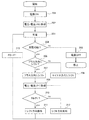
次に、本発明の一態様に係る非接触給電システムにおける給電方法について図1乃至図3を参照して説明する。図3は、非接触給電システムにおける給電方法の一例を示すフローチャートである。
<Power supply method in non-contact power supply system>
Next, a power feeding method in the non-contact power feeding system according to one embodiment of the present invention will be described with reference to FIGS. FIG. 3 is a flowchart illustrating an example of a power feeding method in the non-contact power feeding system.
まず、給電装置110に対して、受電装置120が任意の位置に設置されると、給電装置110は受電装置120へ送電を開始する。給電装置110の高周波電源111をオンとすることにより送電が開始される(図3に示すステップ201参照)。このとき、給電装置110の第1の整合回路113のパラメータ及び受電装置120の第2の整合回路123のパラメータは初期状態(例えば、図2(A)に示すNo.0のパラメータセット)であるため、この段階では効率の良い送電が行われているとは限らない。つまり、伝送効率が最大であるとは限らない。なお、本実施の形態では、パラメータセットに付与した番号のNo.1からプラス方向にシフトさせる場合について説明する。
First, when the
給電装置110から受電装置120へ送電が開始されると、給電装置110の第1の共鳴用コイル112から受電装置120の第2の共鳴用コイル122へ、磁気共鳴結合を介して送電され、さらに、整流回路127及びDCDCコンバータ128によって、直流電圧及び直流電流に変換され、負荷121(例えば、二次電池、LED、ICチップのいずれかを少なくとも含む)へ印加される。このとき、受電装置120の第2の制御回路124は、負荷121に印加される直流電圧値及び直流電流値を取得する(図3に示すステップ202参照)。例えば、第2の制御回路124がA/D変換回路を有している場合には、直流電圧値及び直流電流値は、アナログ信号からデジタル信号へ変換されて、第2の制御回路124で取得される。このときの直流電圧値及び直流電流値の積を電力値P0とする。取得した直流電圧値及び直流電流値の積(電力値P0)のデータは、第2の制御回路124に接続された記憶装置(図示せず)に格納してもよい。
When power transmission from the
次に、一定期間(例えば、300msec)、負荷121に充電(又は給電とも記す)を行う(図3に示すステップ203参照)。
Next, the
次に、第2の制御回路124は、負荷121の充電を継続するか否かを判定する(図3に示すステップ204参照)。負荷121の充電を継続しないと判定された場合は、高周波電源111をオフすることで、充電を完了させる(図3に示すステップ205参照)。負荷121の充電を継続すると判定された場合は、次のステップに進む。
Next, the
次に、第2の制御回路124は、パラメータセットをプラス方向にシフトさせるか否かを判定する(図3に示すステップ206参照)。プラス方向にシフトさせないと判定された場合は、パラメータセットをマイナス方向にシフトさせる命令を第2の整合回路123及び第1の整合回路113に出力する(図3に示すステップ208)。プラス方向にシフトさせると判定された場合は、パラメータセットをプラス方向にシフトさせる命令を第2の整合回路123及び第1の整合回路113に出力する(図3に示すステップ207参照)。なお、第2の整合回路123から第1の整合回路113に命令を出力する場合は、第2の制御回路は第2の送受信回路125に命令を出力し、第2の送受信回路125からアンテナ126及びアンテナ116を介して第1の送受信回路115へ送信し、第1の送受信回路115から第1の制御回路114を介して第1の整合回路113へ出力すればよい。
Next, the
次に、第2の制御回路124は、パラメータセットをプラス方向又はマイナス方向にシフトした後の直流電圧値及び直流電流値を取得する(図3に示すステップ209参照)。このときの直流電圧値及び直流電流値の積を電力値P1とする。取得した直流電圧値及び直流電流値の積(電力値P1)のデータは、第2の制御回路124に接続された記憶装置(図示せず)に格納してもよい。
Next, the
次に、第2の制御回路124は、電力値P1が電力値P0よりも大きいか否かを判定する(図3に示すステップ210参照)。第2の制御回路124が、電力値P1が電力値P0よりも小さいと判定した場合は、パラメータセットのシフトの方向を反転させる命令を第2の整合回路123及び第1の整合回路113に出力する(図3に示すステップ212参照)。第2の制御回路124が、電力値P1が電力値P0よりも大きいと判定した場合は、パラメータセットのシフトの方向を維持する命令を第2の整合回路123及び第1の整合回路113に出力する(図3に示すステップ211参照)。
Next, the
次に、第2の制御回路124は、電力値P1を電力値P0に代入する(図3に示すステップ213参照)。その後の処理は、ステップ203に戻され、それ以降の処理が繰り返される。すなわち、負荷121の充電が完了するまで、ステップ203〜213のループ処理が繰り返し実行される。
Next, the
例えば、ステップ203〜213のループ処理が繰り返し実行され、第2の制御回路124は、パラメータセットのNo.j−1の直流電圧値及び直流電流値の積(P0=Wj−1)を取得した後、パラメータセットをプラス方向にシフトさせ、パラメータセットのNo.jの直流電圧値及び直流電流値の積(P1=Wj)を取得したとする(図3に示すステップ209参照)。
For example, the loop processing of
次に、第2の制御回路124は、電力値P1が電力値P0よりも大きいか否かを判定し、P1がP0よりも大きい(Wj>Wj−1)と判定したとする(図3に示すステップ210参照)。この場合、パラメータセットのシフトの方向は維持されるという命令が、第2の制御回路124から第2の整合回路123及び第1の整合回路113に出力される(図3に示すステップ211参照)。
Next, the
次に、第2の制御回路124において、電力値P1が電力値P0に代入されるため、P0=Wjとなり(図3に示すステップ213参照)、一定期間、負荷121に充電が行われる(図3に示すステップ203参照)。
Next, in the
次に、第2の制御回路124は、負荷121に充電を継続するか否かを判定し、充電を継続すると判定したとする(図3に示すステップ204)と、ステップ206に進む。
Next, the
次に、第2の制御回路124は、パラメータセットをプラス方向にシフトさせるか否かを判定する(図3に示すステップ206参照)。ここで、パラメータセットをNo.j−1からjにプラス方向にシフトすることで、P0<P1となることが、ステップ210において判定されているため、第2の制御回路124は、パラメータセットをNo.jからj+1にプラス方向にシフトさせる命令を第2の整合回路123及び第1の整合回路113に出力する(図3に示すステップ207参照)。
Next, the
次に、第2の制御回路124は、パラメータセットNo.j+1の直流電圧値及び直流電流値を取得する(図3に示すステップ208参照)。このときの直流電圧値及び直流電流値の積を電力値P1=Wj+1とする。
Next, the
次に、第2の制御回路124は、電力値P1が電力値P0よりも大きいか否かを判定し、P1がP0よりも小さい(Wj<Wj+1)と判定したとする(図3に示すステップ210参照)。この場合は、パラメータセットのシフト方向を反転する命令が第2の整合回路123及び第1の整合回路113に出力される(図3に示すステップ212参照)。
Next, the
次に、第2の制御回路124において、電力値P1が電力値P0に代入されるため、P0=Wj+1となり(図3に示すステップ213)、一定期間、負荷121に充電が行われる(図3に示すステップ203)。
Next, in the
ここで、上述のパラメータセットのNo.と受電電力との関係を図4に示す。図4に示すように、パラメータセットがNo.jのとき、受電電力は極大値をとるとすると、給電装置110と受電装置120との距離がAj[cm]であるときに、電力の伝送効率が最大となる。したがって、パラメータセットがNo.jのときに、給電装置110から受電装置120へ効率よく給電を行うことができる。負荷121の充電が完了するまで、パラメータセットのNo.jとj+1とを繰り返すことにより、効率よく負荷121に充電を行うことができる。
Here, in the above parameter set No. FIG. 4 shows the relationship between and the received power. As shown in FIG. Assuming that the received power has a maximum value at j , the power transmission efficiency is maximized when the distance between the
また、負荷121に充電を行っている途中で、給電装置110と受電装置120との距離が変わった場合であっても、負荷121の充電が完了するまで、パラメータセットのNo.を変更しつづければよいため、効率よく充電を行うことができる。
Further, even when the distance between the
図1に示す非接触給電システムにおいて、図3に示す給電方法を適用することで、給電装置110と受電装置120の配置に応じて、電力の伝送効率を高めることができるため、効率よく、給電を行うことができる。このため、給電利用者にとって、より利便性が高い給電システムを提供することができる。
In the non-contact power supply system shown in FIG. 1, by applying the power supply method shown in FIG. 3, the power transmission efficiency can be increased according to the arrangement of the
次に、図1とは一部異なる非接触給電システムの構成について図5に示す。 Next, FIG. 5 shows a configuration of a non-contact power feeding system that is partially different from FIG.
給電装置140は、高周波電源111、第1のコイル117と、第1の共鳴用コイル112と、容量素子118と、第1の整合回路113と、第1の制御回路114と、第1の送受信回路115と、第1のアンテナ116と、を有する。給電装置140において、高周波電源111は、第1のコイル117と接続されており、第1のコイル117と電磁結合をする第1の共鳴用コイル112が第1の整合回路113と接続されている。また、第1の整合回路113は、第1の制御回路114を介して第1の送受信回路115と接続されている。
The
また、受電装置150は、負荷121と、第2のコイル129と、第2の共鳴用コイル122と、容量素子130と、第2の整合回路123と、第2の制御回路124と、第2の送受信回路125と、第2のアンテナ126と、を有する。受電装置150において、第1の共鳴用コイル112と電磁共鳴をする第2の共鳴用コイル122は、第2の整合回路123と接続されており、第2の共鳴用コイル122と電磁結合をする第2のコイル129が、整流回路127、DCDCコンバータ128を介して負荷121に接続されている。負荷121は、第2の制御回路124と、第2の制御回路124を介して第2の送受信回路125とにそれぞれ接続されている。
The
なお、容量素子118及び容量素子130は、それぞれ第1の共鳴用コイル112及び第2の共鳴用コイル122の寄生容量であってもよいし、それぞれ独立に設けられていてもよい。
Note that the capacitive element 118 and the
給電装置140が有する第1の整合回路113は、第1の共鳴用コイル112と接続された少なくとも一つの素子を有する。また、受電装置150が有する第2の整合回路123は、第2の共鳴用コイル122と接続された少なくとも一つの素子を有する。また、第1の共鳴用コイル112と接続された少なくとも一つの素子は、可変素子(可変容量素子又は可変コイル)であることが好ましい。また、第2の共鳴用コイル122と接続された少なくとも一つの素子は、可変素子(可変容量素子又は可変コイル)であることが好ましい。
The
また、第1の整合回路において、第1の共鳴用コイル112と接続された素子と、第2の整合回路において、第2の共鳴用コイル122と接続された素子とは、同じ構造を有する素子であることが好ましい。例えば、第1の整合回路113において、第1の共鳴用コイル112と接続された素子が、可変容量素子である場合には、第2の整合回路123において、第2の共鳴用コイル122と接続された素子は、可変容量素子であることが好ましい。
In the first matching circuit, the element connected to the
図5に示す非接触給電システムでは、第1の共鳴用コイル112は第1のコイル117と電磁結合をし、第2の共鳴用コイル122は第2のコイル129と電磁結合をし、第1の共鳴用コイル112と第2の共鳴用コイル122が電磁共鳴する方法で、電力の伝送を行う。図5に示す非接触給電システムにおいて、第1の共鳴用コイル112及び第2の共鳴用コイル122のQ値を高めることができるので、図1に示す非接触給電システムと比較して、長距離の電力の伝送が可能であるという特徴を有している。
In the non-contact power supply system shown in FIG. 5, the
図5に示す非接触給電システムにおいても、第1の共鳴用コイル112と第2の共鳴用コイル122との距離毎に、電力の伝送効率が最大となる条件が異なる。
Also in the non-contact power supply system shown in FIG. 5, the conditions under which the power transmission efficiency is maximized are different for each distance between the
例えば、図6(B1)に示すように、第1の共鳴用コイル112と第2の共鳴用コイル122とが任意の位置に設置された場合、図6(B2)に示すように、周波数が共振周波数f0のとき電力の伝送効率は最大となる。しかしながら、図6(A1)に示すように、第1の共鳴用コイル112と第2の共鳴用コイル122との距離が近すぎる場合、図6(A2)の細い実線に示すように、電力の伝送効率にピークのスプリットが発生し、ピークは周波数f0’のときであり、共振周波数f0においてはピークの谷となってしまうため、電力の伝送効率が低下してしまう。また、図6(C1)に示すように、第1の共鳴用コイル112と第2の共鳴用コイル122との距離が離れている場合、図6(C2)ピークスプリットは発生しないが共振周波数f0において、図6(B2)と比較して電力の伝送効率が低くなってしまう。なお、図6では、理解を容易にするため、高周波電源111と、第1のコイル117、第1の共鳴用コイル112、負荷121、第2のコイル129、第2の共鳴用コイル122のみを示している。
For example, as shown in FIG. 6 (B1), when the
図5に示すように、非接触給電システムに第1の整合回路113及び第2の整合回路123を用いることにより、第1の共鳴用コイル112と第2の共鳴用コイル122との距離毎に、電力の伝送効率が最大となる条件が設定することができるため、効率よく給電を行うことができる。
As shown in FIG. 5, by using the
特に、第1の共鳴用コイル112と第2の共鳴用コイル122との距離が近すぎて、電力の伝送効率にピークのスプリットが発生したとしても、第1の整合回路113及び第2の整合回路123を用いることにより、図6(A2)の太い実線に示すように、伝送効率のピークを共振周波数f0にシフトすることができるため、電力の伝送効率を高めることができる。
In particular, even if the distance between the
次に、図5とは一部異なる非接触給電システムについて図7に示す。 Next, FIG. 7 shows a non-contact power feeding system which is partially different from FIG.
給電装置160は、高周波電源111、第1のコイル117と、第1の共鳴用コイル112と、容量素子118と、第1の整合回路113と、第1の制御回路114と、第1の送受信回路115と、第1のアンテナ116と、を有する点においては、図5と同様である。図5と異なる部分は、給電装置160において、高周波電源111は、第1の整合回路113を介して第1のコイル117と接続されており、第1のコイル117と電磁結合をする第1の共鳴用コイル112と、容量素子118が接続されている点にある。
The
また、受電装置170は、負荷121と、第2のコイル129と、第2の共鳴用コイル122と、容量素子130と、第2の整合回路123と、第2の制御回路124と、第2の送受信回路125と、第2のアンテナ126と、を有する点においては、図5と同様である。図5と異なる部分は、受電装置170において、第1の共鳴用コイル112と電磁共鳴をする第2の共鳴用コイル122は、容量素子130と接続され、第2の共鳴用コイル122と電磁結合をする第2のコイル129が、第2の整合回路123、整流回路127、DCDCコンバータ128を介して負荷121に接続されている。
In addition, the
なお、第1の共鳴用コイル112及び第2の共鳴用コイル122は、孤立したコイルを用い、容量素子118及び容量素子130は、それぞれ第1の共鳴用コイル112及び第2の共鳴用コイル122の寄生容量とすることが好ましい。このような構成とすることにより、共鳴用コイルに独立して容量素子を接続する場合と比較してQ値をさらに高めることができる。
Note that the
図5及び図7に示す第1の共鳴用コイル112と容量素子118とによって構成される共振回路、及び第2の共鳴用コイル122と容量素子130とによって構成される共振回路は、Q値が非常に高い。したがって、これらの共振回路に接続された回路に起因して、Q値が低下し、電力の伝送効率が低下してしまうおそれがある。そこで、図7に示すように、高周波電源111側に第1の整合回路を設け、負荷121側に第2の整合回路を設けることにより、Q値の低下を抑制し、電力の伝送効率の低下を抑制することができる。
The resonance circuit constituted by the
図5及び図7の非接触給電システムにおいても、図3に示す給電方法を適用することで、給電装置と受電装置の配置に応じて、電力の伝送効率を高めることができるため、効率よく、給電を行うことができる。このため、給電利用者にとって、より利便性が高い給電システムを提供することができる。 Also in the non-contact power feeding system of FIG. 5 and FIG. 7, by applying the power feeding method shown in FIG. 3, the power transmission efficiency can be increased according to the arrangement of the power feeding device and the power receiving device. Power can be supplied. For this reason, it is possible to provide a power supply system that is more convenient for power supply users.
(実施の形態2)
本実施の形態では、上記実施の形態で説明した非接触給電システムを適用できる用途について説明する。なお、本発明の一態様に係る非接触給電システムを適用できる用途としては、例えば携帯型の電子機器である、デジタルビデオカメラ、携帯情報端末(モバイルコンピュータ、携帯電話、携帯型ゲーム機又は電子書籍等)、記録媒体を備えた画像再生装置(具体的にはDigital Versatile Disc(DVD))などが挙げられる。また、電力を基に動力を得る電気自動車等の電気推進移動体が挙げられる。以下、一例について図面を用いて説明する。
(Embodiment 2)
In this embodiment, a use to which the non-contact power feeding system described in the above embodiment can be applied will be described. Note that examples of applications to which the contactless power supply system according to one embodiment of the present invention can be applied include a digital video camera, a portable information terminal (mobile computer, cellular phone, portable game machine, or electronic book) that are portable electronic devices, for example. Etc.), and an image reproducing apparatus (specifically, Digital Versatile Disc (DVD)) provided with a recording medium. In addition, an electric propulsion moving body such as an electric vehicle that obtains power based on electric power can be used. Hereinafter, an example will be described with reference to the drawings.
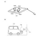
図8(A)は携帯電話及び携帯情報端末を非接触給電システムの用途とする一例であり、給電装置701、受電装置703Aを有する携帯電話702A、受電装置703Bを有する携帯電話702Bによって構成されている。上記実施の形態で説明した非接触給電システムは、給電装置701と受電装置703Aとの間、及び給電装置701と受電装置703Bとの間で適用することができる。
FIG. 8A illustrates an example in which a cellular phone and a portable information terminal are used for a non-contact power feeding system. The cellular phone and a portable information terminal are configured by a
例えば、給電装置701には、実施の形態1に示す給電装置110、140、160の構成が適用でき、受電装置703A及び受電装置703Bには、実施の形態1に示す受電装置120、150、170の構成が適用できる。
For example, the configuration of the
本発明の一態様に係る非接触給電システムを適用することにより、給電装置701と受電装置703Aとの配置、及び給電装置701と受電装置703Bとの配置に応じて、送電の効率を高めることができるため、給電装置701から受電装置703A及び受電装置703Bへ電力を効率よく供給することができる。
By applying the non-contact power feeding system according to one embodiment of the present invention, the efficiency of power transmission can be increased depending on the arrangement of the
図8(B)は電気推進移動体である電気自動車を非接触給電システムの用途とする一例であり、給電装置711、受電装置713を有する電気自動車712によって構成されている。上記実施の形態で説明した非接触給電システムは、給電装置711と受電装置713との間で適用することができる。
FIG. 8B is an example in which an electric vehicle that is an electric propulsion moving body is used for a non-contact power feeding system, and includes an
例えば、給電装置711には、実施の形態1に示す給電装置110、140、160の構成が適用でき、受電装置713には、実施の形態1に示す受電装置120、150、170の構成が適用できる。
For example, the configuration of the
本発明の一態様に係る非接触給電システムを適用することにより、給電装置711と受電装置713との配置に応じて、送電の効率を高めることができるため、給電装置711から受電装置713へ電力を効率よく供給することができる。
By applying the non-contact power feeding system according to one embodiment of the present invention, power transmission efficiency can be increased in accordance with the arrangement of the
また、受電装置713を有する電気自動車712と給電装置711との配置が変わったとしても、図2(A)に示すようなパラメータセットの範囲内であれば、送電の効率を変化させることができるため、送電の効率を高めることができる。
Further, even if the arrangement of the
以上、上記実施の形態で説明した非接触給電システムは電力をもって駆動させる物品であればどのようなものにでも設けて使用することができる。 As described above, the non-contact power feeding system described in the above embodiment can be provided and used for any article that is driven with electric power.
本実施の形態は、他の実施の形態に記載した構成と適宜組み合わせて実施することが可能である。 This embodiment can be implemented in appropriate combination with the structures described in the other embodiments.
110 給電装置
111 高周波電源
112 共鳴用コイル
113 整合回路
114 制御回路
115 送受信回路
116 アンテナ
117 コイル
118 容量素子
120 受電装置
121 負荷
122 共鳴用コイル
123 整合回路
124 制御回路
125 送受信回路
126 アンテナ
127 整流回路
128 DCDCコンバータ
129 コイル
130 容量素子
140 給電装置
150 受電装置
160 給電装置
170 受電装置
201 ステップ
202 ステップ
203 ステップ
204 ステップ
205 ステップ
206 ステップ
207 ステップ
208 ステップ
209 ステップ
210 ステップ
211 ステップ
212 ステップ
213 ステップ
701 給電装置
702A 携帯電話
702B 携帯電話
703A 受電装置
703B 受電装置
711 給電装置
712 電気自動車
713 受電装置
DESCRIPTION OF
Claims (4)
前記給電装置は、高周波電源、第1の整合回路、第1の共鳴用コイル、第1の送受信回路、第1の制御回路及び第1のアンテナを有し、
前記高周波電源は前記第1の整合回路を介して前記第1の共鳴用コイルと接続され、
前記第1の制御回路は、前記第1の整合回路及び第1の送受信回路とそれぞれ接続され、
前記第1の送受信回路は前記第1のアンテナと接続され、
前記受電装置は、第2の整合回路、第2の共鳴用コイル、第2の送受信回路、第2の制御回路、負荷及び第2のアンテナを有し、
前記第2の共鳴用コイルは、前記第1の共鳴用コイルと電磁共鳴をし、
前記第2の共鳴用コイルは前記第2の整合回路と接続され、
前記第2の制御回路は、前記負荷、前記第2の整合回路、及び前記第2の送受信回路とそれぞれ接続され、
前記第2の送受信回路は前記第2のアンテナと接続され、
前記第2の制御回路は、前記負荷に印加される直流電圧値及び直流電流値を取得する機能を有し、
前記第2の制御回路は、取得した前記直流電圧値及び前記直流電流値に基づき、前記第1の整合回路及び前記第2の整合回路に命令を出力する機能を有し、
前記第2の制御回路から前記第1の整合回路への命令の出力は、前記第2の送受信回路、前記第2のアンテナ及び前記第1のアンテナを介して行われ、
前記第1の整合回路のパラメータと前記第2の整合回路のパラメータとのパラメータセットは、前記給電装置と前記受電装置との距離に応じて設定されることを特徴とする非接触給電システム。 A power feeding device and a power receiving device;
The power supply apparatus includes a high frequency power source, a first matching circuit, a first resonance coil, a first transmission / reception circuit, a first control circuit, and a first antenna,
The high-frequency power source is connected to the first resonance coil via the first matching circuit,
The first control circuit is connected to the first matching circuit and the first transmission / reception circuit, respectively.
The first transmission / reception circuit is connected to the first antenna;
The power receiving device includes a second matching circuit, a second resonance coil, a second transmission / reception circuit, a second control circuit, a load, and a second antenna.
The second resonance coil performs electromagnetic resonance with the first resonance coil;
The second resonance coil is connected to the second matching circuit;
The second control circuit is connected to the load, the second matching circuit, and the second transmission / reception circuit, respectively.
The second transmission / reception circuit is connected to the second antenna;
The second control circuit has a function of acquiring a DC voltage value and a DC current value applied to the load,
The second control circuit has a function of outputting a command to the first matching circuit and the second matching circuit based on the acquired DC voltage value and the DC current value,
The output of the command from the second control circuit to the first matching circuit is performed via the second transmission / reception circuit, the second antenna, and the first antenna.
The non-contact power feeding system according to claim 1, wherein a parameter set of the first matching circuit parameter and the second matching circuit parameter is set according to a distance between the power feeding device and the power receiving device.
前記給電装置と前記受電装置との距離に応じて、前記パラメータセットは0番からn番(nは整数)まで設定され、
前記負荷の充電が完了するまで、前記第1の整合回路と前記第2の整合回路とは、前記給電装置と前記受電装置との間の電力の伝送効率が最大となるj(j≦n−1)番目のパラメータセットと、j+1番目のパラメータセットとを繰り返すことを特徴とする非接触給電システム。 In claim 1,
According to the distance between the power feeding device and the power receiving device, the parameter set is set from 0 to n (n is an integer),
Until the charging of the load is completed, the first matching circuit and the second matching circuit have j (j ≦ n−) that maximizes the power transmission efficiency between the power feeding device and the power receiving device. 1) A non-contact power feeding system characterized by repeating a first parameter set and a j + 1th parameter set.
前記第1の整合回路は、前記高周波電源と直列に接続された第1の素子と、前記高周波電源と並列に接続された第2の素子とを有し、
前記第2の整合回路は、前記負荷と直列に接続された第3の素子と、前記負荷と並列に接続された第4の素子と、を有することを特徴とする非接触給電システム。 In claim 1 or claim 2,
The first matching circuit includes a first element connected in series with the high-frequency power source, and a second element connected in parallel with the high-frequency power source,
The second matching circuit includes a third element connected in series with the load, and a fourth element connected in parallel with the load.
前記第1の素子及び前記第3の素子は、可変容量素子であり、
前記第2の素子及び前記第4の素子は、可変コイルであることを特徴とする非接触給電システム。 In claim 3 ,
The first element and the third element are variable capacitance elements,
The non-contact power feeding system, wherein the second element and the fourth element are variable coils.
Priority Applications (1)
| Application Number | Priority Date | Filing Date | Title |
|---|---|---|---|
| JP2011277792A JP5947534B2 (en) | 2010-12-24 | 2011-12-20 | Contactless power supply system |
Applications Claiming Priority (3)
| Application Number | Priority Date | Filing Date | Title |
|---|---|---|---|
| JP2010287551 | 2010-12-24 | ||
| JP2010287551 | 2010-12-24 | ||
| JP2011277792A JP5947534B2 (en) | 2010-12-24 | 2011-12-20 | Contactless power supply system |
Publications (3)
| Publication Number | Publication Date |
|---|---|
| JP2012147657A JP2012147657A (en) | 2012-08-02 |
| JP2012147657A5 JP2012147657A5 (en) | 2015-01-15 |
| JP5947534B2 true JP5947534B2 (en) | 2016-07-06 |
Family
ID=46315737
Family Applications (1)
| Application Number | Title | Priority Date | Filing Date |
|---|---|---|---|
| JP2011277792A Expired - Fee Related JP5947534B2 (en) | 2010-12-24 | 2011-12-20 | Contactless power supply system |
Country Status (4)
| Country | Link |
|---|---|
| US (1) | US9065302B2 (en) |
| JP (1) | JP5947534B2 (en) |
| KR (1) | KR101871148B1 (en) |
| TW (1) | TWI539709B (en) |
Families Citing this family (25)
| Publication number | Priority date | Publication date | Assignee | Title |
|---|---|---|---|---|
| US10715209B2 (en) * | 2006-11-18 | 2020-07-14 | RF Micron, Inc. | Computing device for processing environmental sensed conditions |
| US10149177B2 (en) * | 2006-11-18 | 2018-12-04 | Rfmicron, Inc. | Wireless sensor including an RF signal circuit |
| KR20120084659A (en) | 2011-01-20 | 2012-07-30 | 가부시키가이샤 한도오따이 에네루기 켄큐쇼 | Power feeding device and wireless power feeding system |
| US9502920B2 (en) | 2011-11-16 | 2016-11-22 | Semiconductor Energy Laboratory Co., Ltd. | Power receiving device, power transmission device, and power feeding system |
| US9673867B2 (en) | 2012-03-14 | 2017-06-06 | Semiconductor Energy Laboratory Co., Ltd. | Power transmission device and power feeding system |
| US8827889B2 (en) | 2012-05-21 | 2014-09-09 | University Of Washington Through Its Center For Commercialization | Method and system for powering implantable devices |
| US11621583B2 (en) | 2012-05-21 | 2023-04-04 | University Of Washington | Distributed control adaptive wireless power transfer system |
| JP6089330B2 (en) * | 2012-08-10 | 2017-03-08 | パナソニックIpマネジメント株式会社 | Small electric device and non-contact power transmission device having the same |
| TWI473382B (en) | 2012-09-28 | 2015-02-11 | Au Optronics Corp | Wireless power transmission device |
| TWI446680B (en) * | 2012-10-30 | 2014-07-21 | Au Optronics Corp | Displaying device and wireless power transmission system |
| US9768643B2 (en) | 2012-11-02 | 2017-09-19 | Panasonic Intellectual Property Management Co., Ltd. | Wireless power transmission system capable of continuing power transmission while suppressing heatup of foreign objects |
| US9276435B2 (en) | 2012-11-02 | 2016-03-01 | Maishi Electronic (Shanghai) Ltd. | Method and apparatus for wirelessly receiving power |
| WO2015018334A1 (en) * | 2013-08-06 | 2015-02-12 | The University Of Hong Kong | Methods for parameter identification, load monitoring and output power control in wireless power transfer systems |
| JP6426402B2 (en) * | 2013-08-30 | 2018-11-21 | 株式会社半導体エネルギー研究所 | Display device |
| CN103595109B (en) * | 2013-12-03 | 2016-03-30 | 东南大学 | A kind of electric automobile mobile charging method and apparatus |
| JP6052149B2 (en) | 2013-12-06 | 2016-12-27 | ソニー株式会社 | Power receiving device, power receiving control method, non-contact power feeding system, and electronic device |
| CN106374639A (en) * | 2015-07-21 | 2017-02-01 | 中兴通讯股份有限公司 | Energy conversion apparatus and method |
| US10263473B2 (en) * | 2016-02-02 | 2019-04-16 | Witricity Corporation | Controlling wireless power transfer systems |
| JP2017184605A (en) * | 2016-03-25 | 2017-10-05 | 古河電気工業株式会社 | Power transmission and reception system and power reception apparatus |
| JP2017184563A (en) * | 2016-03-31 | 2017-10-05 | 古河電気工業株式会社 | Power transmission and reception system and power transmission apparatus |
| JP6754669B2 (en) * | 2016-10-31 | 2020-09-16 | 株式会社ダイヘン | Power supply side device and power supply system |
| CN109412276B (en) | 2017-08-15 | 2022-08-12 | 泰达电子股份有限公司 | Control circuit and control method suitable for wireless power transmission device |
| JP7089882B2 (en) * | 2018-01-16 | 2022-06-23 | 清水建設株式会社 | Wireless power transmission system and wireless power transmission method |
| US20210351619A1 (en) * | 2020-05-06 | 2021-11-11 | Hamilton Sundstrand Corporation | Inductive power transfer in deep space and remote applications |
| TWI741958B (en) * | 2021-03-05 | 2021-10-01 | 國立陽明交通大學 | Minimum power input control method |
Family Cites Families (72)
| Publication number | Priority date | Publication date | Assignee | Title |
|---|---|---|---|---|
| NL8901659A (en) | 1989-06-30 | 1991-01-16 | Nedap Nv | MULTIPASS SYSTEM. |
| JPH066272A (en) | 1992-06-17 | 1994-01-14 | Omron Corp | Pulse receiving circuit of data communication equipment |
| JP2803943B2 (en) | 1992-10-21 | 1998-09-24 | アルプス電気株式会社 | Non-contact power supply |
| US5790946A (en) | 1993-07-15 | 1998-08-04 | Rotzoll; Robert R. | Wake up device for a communications system |
| JPH087059A (en) | 1994-06-21 | 1996-01-12 | Sony Chem Corp | Noncontact information card |
| JPH10285087A (en) | 1997-04-10 | 1998-10-23 | Omron Corp | Data carrier and identification system |
| JP3940939B2 (en) | 1997-09-08 | 2007-07-04 | 吉川アールエフシステム株式会社 | Data carrier |
| US6837438B1 (en) | 1998-10-30 | 2005-01-04 | Hitachi Maxell, Ltd. | Non-contact information medium and communication system utilizing the same |
| US6509217B1 (en) | 1999-10-22 | 2003-01-21 | Damoder Reddy | Inexpensive, reliable, planar RFID tag structure and method for making same |
| JP3488166B2 (en) * | 2000-02-24 | 2004-01-19 | 日本電信電話株式会社 | Contactless IC card system, its reader / writer and contactless IC card |
| US20020049714A1 (en) | 2000-05-11 | 2002-04-25 | Shunpei Yamazaki | Communication system |
| US7209771B2 (en) | 2000-12-22 | 2007-04-24 | Terahop Networks, Inc. | Battery powered wireless transceiver having LPRF component and second wake up receiver |
| JP2002259921A (en) | 2001-03-02 | 2002-09-13 | Denso Corp | Id tag and receiving power control method of id tag |
| US6944424B2 (en) | 2001-07-23 | 2005-09-13 | Intermec Ip Corp. | RFID tag having combined battery and passive power source |
| JP2003085506A (en) | 2001-09-12 | 2003-03-20 | Yoshikawa Rf System Kk | Overvoltage preventing circuit in data carrier |
| US6737302B2 (en) | 2001-10-31 | 2004-05-18 | Semiconductor Energy Laboratory Co., Ltd. | Manufacturing method for field-effect transistor |
| US7215976B2 (en) | 2001-11-30 | 2007-05-08 | Symbol Technologies, Inc. | RFID device, system and method of operation including a hybrid backscatter-based RFID tag protocol compatible with RFID, bluetooth and/or IEEE 802.11x infrastructure |
| JP3866594B2 (en) | 2002-03-15 | 2007-01-10 | Necエレクトロニクス株式会社 | Delay circuit, semiconductor memory device, and control method of semiconductor memory device |
| JP4719852B2 (en) | 2002-10-18 | 2011-07-06 | シンボル テクノロジーズ, インコーポレイテッド | System and method for minimizing unnecessary renegotiation of passive RFID tags |
| US7072697B2 (en) | 2002-10-22 | 2006-07-04 | Nokia Corporation | Method and device for transponder aided wake-up of a low power radio device by a wake-up event |
| US7652359B2 (en) | 2002-12-27 | 2010-01-26 | Semiconductor Energy Laboratory Co., Ltd. | Article having display device |
| US7603144B2 (en) | 2003-01-02 | 2009-10-13 | Cymbet Corporation | Active wireless tagging system on peel and stick substrate |
| JP2005063123A (en) | 2003-08-11 | 2005-03-10 | Fuji Electric Holdings Co Ltd | Reader/writer device for non-contact card and method for automatically adjusting its antenna natural frequency, and program |
| JP2005235615A (en) | 2004-02-20 | 2005-09-02 | Hitachi Maxell Ltd | Adapter panel, electronic equipment and cable connector recognition system |
| JP4611093B2 (en) | 2004-05-12 | 2011-01-12 | セイコーインスツル株式会社 | Radio power generation circuit |
| ATE511159T1 (en) | 2004-07-01 | 2011-06-15 | Powerid Ltd | BATTERY-ASSISTED BACKSCATTER RFID TRANSPONDER |
| JP2006024087A (en) | 2004-07-09 | 2006-01-26 | Nec Corp | Radio device, its manufacturing method, its inspecting method and inspecting device, radio apparatus, and its manufacturing method |
| JP4519599B2 (en) | 2004-10-07 | 2010-08-04 | 株式会社半導体エネルギー研究所 | Semiconductor device |
| US20060103533A1 (en) | 2004-11-15 | 2006-05-18 | Kourosh Pahlavan | Radio frequency tag and reader with asymmetric communication bandwidth |
| JP2006180073A (en) | 2004-12-21 | 2006-07-06 | Okayama Prefecture | Wireless ic tag |
| JP2007183790A (en) | 2006-01-06 | 2007-07-19 | Hitachi Ltd | Rfid device, rfid system and access control method |
| KR101362954B1 (en) | 2006-03-10 | 2014-02-12 | 가부시키가이샤 한도오따이 에네루기 켄큐쇼 | Semiconductor device and method for operating the same |
| WO2007105607A1 (en) | 2006-03-10 | 2007-09-20 | Semiconductor Energy Laboratory Co., Ltd. | Semiconductor device |
| WO2007108371A1 (en) | 2006-03-15 | 2007-09-27 | Semiconductor Energy Laboratory Co., Ltd. | Semiconductor device |
| CN103078368B (en) | 2006-03-15 | 2016-04-13 | 株式会社半导体能源研究所 | Electric power supply system and the electric power supply system for motor vehicle |
| EP2002383B1 (en) | 2006-03-15 | 2012-04-25 | Semiconductor Energy Laboratory Co., Ltd. | Semiconductor device |
| WO2007139205A1 (en) | 2006-05-31 | 2007-12-06 | Semiconductor Energy Laboratory Co., Ltd. | Semiconductor device and ic label, ic tag, and ic card having the same |
| US8132026B2 (en) | 2006-06-02 | 2012-03-06 | Semiconductor Energy Laboratory Co., Ltd. | Power storage device and mobile electronic device having the same |
| DE602007013986D1 (en) | 2006-10-18 | 2011-06-01 | Semiconductor Energy Lab | ID radio transponder |
| US20090160261A1 (en) | 2007-12-19 | 2009-06-25 | Nokia Corporation | Wireless energy transfer |
| US8855554B2 (en) * | 2008-03-05 | 2014-10-07 | Qualcomm Incorporated | Packaging and details of a wireless power device |
| JP2009268181A (en) | 2008-04-22 | 2009-11-12 | Olympus Corp | Energy supply apparatus |
| JP4911148B2 (en) | 2008-09-02 | 2012-04-04 | ソニー株式会社 | Contactless power supply |
| JP5288958B2 (en) | 2008-09-11 | 2013-09-11 | 矢崎総業株式会社 | Wireless power transmission apparatus and resonance frequency adjustment method |
| JP2012504387A (en) * | 2008-09-27 | 2012-02-16 | ウィトリシティ コーポレーション | Wireless energy transfer system |
| JP5258521B2 (en) | 2008-11-14 | 2013-08-07 | トヨタ自動車株式会社 | Power supply system |
| JP5351499B2 (en) * | 2008-11-28 | 2013-11-27 | 長野日本無線株式会社 | Contactless power transmission system |
| JP5114371B2 (en) * | 2008-12-09 | 2013-01-09 | 株式会社豊田自動織機 | Non-contact power transmission device |
| KR101248453B1 (en) | 2008-12-09 | 2013-04-01 | 도요타지도샤가부시키가이샤 | Non-contact power transmission apparatus and power transmission method using a non-contact power transmission apparatus |
| JP5114372B2 (en) * | 2008-12-09 | 2013-01-09 | 株式会社豊田自動織機 | Power transmission method and non-contact power transmission apparatus in non-contact power transmission apparatus |
| JP2010193598A (en) | 2009-02-17 | 2010-09-02 | Nippon Soken Inc | Noncontact power supply facility and noncontact power supply system |
| JP5621203B2 (en) | 2009-03-30 | 2014-11-12 | 富士通株式会社 | Wireless power supply system and wireless power supply method |
| JP5417941B2 (en) | 2009-03-31 | 2014-02-19 | 富士通株式会社 | Power transmission equipment |
| JP4865001B2 (en) | 2009-04-13 | 2012-02-01 | 株式会社日本自動車部品総合研究所 | Non-contact power supply equipment, non-contact power receiving device and non-contact power supply system |
| JP5481091B2 (en) | 2009-04-14 | 2014-04-23 | 富士通テン株式会社 | Wireless power transmission apparatus and wireless power transmission method |
| JP2010252468A (en) | 2009-04-14 | 2010-11-04 | Sony Corp | Power transmission device and method, power receiving device and method, and power transmission system |
| JP5347708B2 (en) | 2009-05-18 | 2013-11-20 | トヨタ自動車株式会社 | Coil unit, non-contact power transmission device, non-contact power feeding system, and vehicle |
| JP2010284006A (en) | 2009-06-05 | 2010-12-16 | Nec Tokin Corp | Non-contact power transmission apparatus |
| JP2010284066A (en) | 2009-06-08 | 2010-12-16 | Nec Tokin Corp | Communication device, communication terminal and communication system |
| JP2011050140A (en) | 2009-08-26 | 2011-03-10 | Sony Corp | Non-contact electric power feeding apparatus, non-contact power electric receiver receiving apparatus, non-contact electric power feeding method, non-contact electric power receiving method and non-contact electric power feeding system |
| JP5499955B2 (en) | 2009-10-05 | 2014-05-21 | Tdk株式会社 | Wireless power supply apparatus and wireless power transmission system |
| JP5664019B2 (en) | 2009-10-28 | 2015-02-04 | Tdk株式会社 | Wireless power feeder, wireless power transmission system, and table and table lamp using the same |
| JP5664018B2 (en) | 2009-10-30 | 2015-02-04 | Tdk株式会社 | Wireless power feeder, wireless power transmission system, and table and table lamp using the same |
| JP5515701B2 (en) | 2009-12-04 | 2014-06-11 | ソニー株式会社 | Power transmission device, power reception device, and power transmission control method |
| JP5304624B2 (en) | 2009-12-10 | 2013-10-02 | トヨタ自動車株式会社 | Power supply device, vehicle, and vehicle power supply system |
| JP2011125184A (en) | 2009-12-14 | 2011-06-23 | Toyota Motor Corp | Noncontact power supply facility, noncontact power receiving apparatus, and noncontact power supply system |
| JP5487944B2 (en) | 2009-12-18 | 2014-05-14 | 日産自動車株式会社 | Non-contact power feeding device |
| JP2011135717A (en) | 2009-12-25 | 2011-07-07 | Toko Inc | Wireless power transmission system |
| JP2011142769A (en) | 2010-01-08 | 2011-07-21 | Toyota Central R&D Labs Inc | Method and device for transmitting magnetic resonance power |
| JP2011142559A (en) | 2010-01-08 | 2011-07-21 | Sony Corp | Power feeding device, power receiving device, and wireless feeding system |
| JP2011223739A (en) | 2010-04-09 | 2011-11-04 | Sony Corp | Power supply device, power reception device, and wireless power supply system |
| EP2571140B1 (en) * | 2010-05-14 | 2018-04-25 | Kabushiki Kaisha Toyota Jidoshokki | Resonance-type non-contact power supply system, and adjustment method for matching unit during charging of resonance-type non-contact power supply system |
-
2011
- 2011-12-07 US US13/313,503 patent/US9065302B2/en not_active Expired - Fee Related
- 2011-12-16 TW TW100146852A patent/TWI539709B/en not_active IP Right Cessation
- 2011-12-20 JP JP2011277792A patent/JP5947534B2/en not_active Expired - Fee Related
- 2011-12-21 KR KR1020110138833A patent/KR101871148B1/en active IP Right Grant
Also Published As
| Publication number | Publication date |
|---|---|
| US9065302B2 (en) | 2015-06-23 |
| KR20120073112A (en) | 2012-07-04 |
| TWI539709B (en) | 2016-06-21 |
| US20120161536A1 (en) | 2012-06-28 |
| TW201236302A (en) | 2012-09-01 |
| JP2012147657A (en) | 2012-08-02 |
| KR101871148B1 (en) | 2018-06-27 |
Similar Documents
| Publication | Publication Date | Title |
|---|---|---|
| JP5947534B2 (en) | Contactless power supply system | |
| US10491183B2 (en) | Power feeding device and wireless power feeding system | |
| US11843259B2 (en) | Power feeding device, power receiving device, and wireless power feed system | |
| JP5798455B2 (en) | Power supply device | |
| US8981599B2 (en) | Power feeding device and contactless power feeding system provided with power feeding device | |
| JP6768902B2 (en) | Power receiving device | |
| JP2020120580A (en) | Operation method for power feeding system | |
| US9941742B2 (en) | Wireless power transmission apparatus and wireless power transmission method | |
| JP5960438B2 (en) | Power supply system and power supply method |
Legal Events
| Date | Code | Title | Description |
|---|---|---|---|
| A521 | Request for written amendment filed |
Free format text: JAPANESE INTERMEDIATE CODE: A523 Effective date: 20141119 |
|
| A621 | Written request for application examination |
Free format text: JAPANESE INTERMEDIATE CODE: A621 Effective date: 20141119 |
|
| A977 | Report on retrieval |
Free format text: JAPANESE INTERMEDIATE CODE: A971007 Effective date: 20150817 |
|
| A131 | Notification of reasons for refusal |
Free format text: JAPANESE INTERMEDIATE CODE: A131 Effective date: 20150825 |
|
| A521 | Request for written amendment filed |
Free format text: JAPANESE INTERMEDIATE CODE: A523 Effective date: 20150923 |
|
| A131 | Notification of reasons for refusal |
Free format text: JAPANESE INTERMEDIATE CODE: A131 Effective date: 20160126 |
|
| A521 | Request for written amendment filed |
Free format text: JAPANESE INTERMEDIATE CODE: A523 Effective date: 20160129 |
|
| TRDD | Decision of grant or rejection written | ||
| A01 | Written decision to grant a patent or to grant a registration (utility model) |
Free format text: JAPANESE INTERMEDIATE CODE: A01 Effective date: 20160531 |
|
| A61 | First payment of annual fees (during grant procedure) |
Free format text: JAPANESE INTERMEDIATE CODE: A61 Effective date: 20160603 |
|
| R150 | Certificate of patent or registration of utility model |
Ref document number: 5947534 Country of ref document: JP Free format text: JAPANESE INTERMEDIATE CODE: R150 |
|
| R250 | Receipt of annual fees |
Free format text: JAPANESE INTERMEDIATE CODE: R250 |
|
| R250 | Receipt of annual fees |
Free format text: JAPANESE INTERMEDIATE CODE: R250 |
|
| R250 | Receipt of annual fees |
Free format text: JAPANESE INTERMEDIATE CODE: R250 |
|
| LAPS | Cancellation because of no payment of annual fees |