JP5915537B2 - IMAGING ELEMENT AND IMAGING DEVICE - Google Patents
IMAGING ELEMENT AND IMAGING DEVICE Download PDFInfo
- Publication number
- JP5915537B2 JP5915537B2 JP2012546697A JP2012546697A JP5915537B2 JP 5915537 B2 JP5915537 B2 JP 5915537B2 JP 2012546697 A JP2012546697 A JP 2012546697A JP 2012546697 A JP2012546697 A JP 2012546697A JP 5915537 B2 JP5915537 B2 JP 5915537B2
- Authority
- JP
- Japan
- Prior art keywords
- photoelectric conversion
- parallax
- conversion element
- pixel
- pixels
- Prior art date
- Legal status (The legal status is an assumption and is not a legal conclusion. Google has not performed a legal analysis and makes no representation as to the accuracy of the status listed.)
- Active
Links
- 238000003384 imaging method Methods 0.000 title claims description 43
- 238000006243 chemical reaction Methods 0.000 claims description 183
- 230000004907 flux Effects 0.000 claims description 48
- 230000003252 repetitive effect Effects 0.000 description 73
- 230000002093 peripheral effect Effects 0.000 description 43
- 238000010586 diagram Methods 0.000 description 34
- 230000003287 optical effect Effects 0.000 description 17
- 238000000034 method Methods 0.000 description 13
- 230000006870 function Effects 0.000 description 12
- 230000010363 phase shift Effects 0.000 description 12
- 210000001747 pupil Anatomy 0.000 description 10
- 239000000758 substrate Substances 0.000 description 10
- 230000008569 process Effects 0.000 description 9
- 238000004519 manufacturing process Methods 0.000 description 7
- 229910052751 metal Inorganic materials 0.000 description 6
- 239000002184 metal Substances 0.000 description 6
- 238000003491 array Methods 0.000 description 5
- 239000011810 insulating material Substances 0.000 description 4
- 239000000463 material Substances 0.000 description 4
- 230000006872 improvement Effects 0.000 description 3
- 230000000737 periodic effect Effects 0.000 description 3
- 238000004528 spin coating Methods 0.000 description 3
- VYPSYNLAJGMNEJ-UHFFFAOYSA-N Silicium dioxide Chemical compound O=[Si]=O VYPSYNLAJGMNEJ-UHFFFAOYSA-N 0.000 description 2
- 239000003086 colorant Substances 0.000 description 2
- 238000005530 etching Methods 0.000 description 2
- 230000004048 modification Effects 0.000 description 2
- 238000012986 modification Methods 0.000 description 2
- 230000035945 sensitivity Effects 0.000 description 2
- 229910052814 silicon oxide Inorganic materials 0.000 description 2
- RYGMFSIKBFXOCR-UHFFFAOYSA-N Copper Chemical compound [Cu] RYGMFSIKBFXOCR-UHFFFAOYSA-N 0.000 description 1
- 229910001218 Gallium arsenide Inorganic materials 0.000 description 1
- 229910052581 Si3N4 Inorganic materials 0.000 description 1
- 230000009471 action Effects 0.000 description 1
- 229910052782 aluminium Inorganic materials 0.000 description 1
- XAGFODPZIPBFFR-UHFFFAOYSA-N aluminium Chemical compound [Al] XAGFODPZIPBFFR-UHFFFAOYSA-N 0.000 description 1
- 230000008859 change Effects 0.000 description 1
- 238000004040 coloring Methods 0.000 description 1
- 230000006835 compression Effects 0.000 description 1
- 238000007906 compression Methods 0.000 description 1
- 239000004020 conductor Substances 0.000 description 1
- 229910052802 copper Inorganic materials 0.000 description 1
- 239000010949 copper Substances 0.000 description 1
- 238000013481 data capture Methods 0.000 description 1
- 239000006185 dispersion Substances 0.000 description 1
- 238000001312 dry etching Methods 0.000 description 1
- 125000005397 methacrylic acid ester group Chemical group 0.000 description 1
- 229910052594 sapphire Inorganic materials 0.000 description 1
- 239000010980 sapphire Substances 0.000 description 1
- 239000004065 semiconductor Substances 0.000 description 1
- 229910052710 silicon Inorganic materials 0.000 description 1
- 239000010703 silicon Substances 0.000 description 1
- HQVNEWCFYHHQES-UHFFFAOYSA-N silicon nitride Chemical compound N12[Si]34N5[Si]62N3[Si]51N64 HQVNEWCFYHHQES-UHFFFAOYSA-N 0.000 description 1
- WFKWXMTUELFFGS-UHFFFAOYSA-N tungsten Chemical compound [W] WFKWXMTUELFFGS-UHFFFAOYSA-N 0.000 description 1
- 229910052721 tungsten Inorganic materials 0.000 description 1
- 239000010937 tungsten Substances 0.000 description 1
- 230000000007 visual effect Effects 0.000 description 1
- 230000037303 wrinkles Effects 0.000 description 1
Images


Classifications
-
- H—ELECTRICITY
- H04—ELECTRIC COMMUNICATION TECHNIQUE
- H04N—PICTORIAL COMMUNICATION, e.g. TELEVISION
- H04N13/00—Stereoscopic video systems; Multi-view video systems; Details thereof
- H04N13/20—Image signal generators
- H04N13/257—Colour aspects
-
- H—ELECTRICITY
- H01—ELECTRIC ELEMENTS
- H01L—SEMICONDUCTOR DEVICES NOT COVERED BY CLASS H10
- H01L27/00—Devices consisting of a plurality of semiconductor or other solid-state components formed in or on a common substrate
- H01L27/14—Devices consisting of a plurality of semiconductor or other solid-state components formed in or on a common substrate including semiconductor components sensitive to infrared radiation, light, electromagnetic radiation of shorter wavelength or corpuscular radiation and specially adapted either for the conversion of the energy of such radiation into electrical energy or for the control of electrical energy by such radiation
- H01L27/144—Devices controlled by radiation
- H01L27/146—Imager structures
- H01L27/14601—Structural or functional details thereof
- H01L27/1462—Coatings
- H01L27/14621—Colour filter arrangements
-
- H—ELECTRICITY
- H01—ELECTRIC ELEMENTS
- H01L—SEMICONDUCTOR DEVICES NOT COVERED BY CLASS H10
- H01L27/00—Devices consisting of a plurality of semiconductor or other solid-state components formed in or on a common substrate
- H01L27/14—Devices consisting of a plurality of semiconductor or other solid-state components formed in or on a common substrate including semiconductor components sensitive to infrared radiation, light, electromagnetic radiation of shorter wavelength or corpuscular radiation and specially adapted either for the conversion of the energy of such radiation into electrical energy or for the control of electrical energy by such radiation
- H01L27/144—Devices controlled by radiation
- H01L27/146—Imager structures
- H01L27/14601—Structural or functional details thereof
- H01L27/1462—Coatings
- H01L27/14623—Optical shielding
-
- H—ELECTRICITY
- H01—ELECTRIC ELEMENTS
- H01L—SEMICONDUCTOR DEVICES NOT COVERED BY CLASS H10
- H01L27/00—Devices consisting of a plurality of semiconductor or other solid-state components formed in or on a common substrate
- H01L27/14—Devices consisting of a plurality of semiconductor or other solid-state components formed in or on a common substrate including semiconductor components sensitive to infrared radiation, light, electromagnetic radiation of shorter wavelength or corpuscular radiation and specially adapted either for the conversion of the energy of such radiation into electrical energy or for the control of electrical energy by such radiation
- H01L27/144—Devices controlled by radiation
- H01L27/146—Imager structures
- H01L27/14601—Structural or functional details thereof
- H01L27/14625—Optical elements or arrangements associated with the device
- H01L27/14627—Microlenses
-
- H—ELECTRICITY
- H01—ELECTRIC ELEMENTS
- H01L—SEMICONDUCTOR DEVICES NOT COVERED BY CLASS H10
- H01L27/00—Devices consisting of a plurality of semiconductor or other solid-state components formed in or on a common substrate
- H01L27/14—Devices consisting of a plurality of semiconductor or other solid-state components formed in or on a common substrate including semiconductor components sensitive to infrared radiation, light, electromagnetic radiation of shorter wavelength or corpuscular radiation and specially adapted either for the conversion of the energy of such radiation into electrical energy or for the control of electrical energy by such radiation
- H01L27/144—Devices controlled by radiation
- H01L27/146—Imager structures
- H01L27/14601—Structural or functional details thereof
- H01L27/14625—Optical elements or arrangements associated with the device
- H01L27/14629—Reflectors
-
- H—ELECTRICITY
- H04—ELECTRIC COMMUNICATION TECHNIQUE
- H04N—PICTORIAL COMMUNICATION, e.g. TELEVISION
- H04N13/00—Stereoscopic video systems; Multi-view video systems; Details thereof
- H04N13/20—Image signal generators
- H04N13/204—Image signal generators using stereoscopic image cameras
- H04N13/207—Image signal generators using stereoscopic image cameras using a single 2D image sensor
- H04N13/225—Image signal generators using stereoscopic image cameras using a single 2D image sensor using parallax barriers
-
- H—ELECTRICITY
- H04—ELECTRIC COMMUNICATION TECHNIQUE
- H04N—PICTORIAL COMMUNICATION, e.g. TELEVISION
- H04N13/00—Stereoscopic video systems; Multi-view video systems; Details thereof
- H04N13/20—Image signal generators
- H04N13/286—Image signal generators having separate monoscopic and stereoscopic modes
Description
本発明は、撮像素子、及び、撮像装置に関する。 The present invention relates to an imaging element and an imaging apparatus.
2つの撮影光学系を用いて、右目用の画像と左目用の画像とから成るステレオ画像を撮像するステレオ撮像装置が知られている。このようなステレオ撮像装置は、2つの撮像光学系を一定の間隔で配置することにより、同一の被写体を撮像して得られる2つの画像に視差を生じさせる。
[先行技術文献]
[特許文献]
[特許文献1] 特開平8−47001号公報A stereo imaging device that captures a stereo image composed of a right-eye image and a left-eye image using two imaging optical systems is known. Such a stereo imaging device causes parallax to occur in two images obtained by imaging the same subject by arranging two imaging optical systems at regular intervals.
[Prior art documents]
[Patent Literature]
[Patent Document 1] JP-A-8-47001
しかしながら、複数の視差を生じさせる画像を取得するには、その数に応じた複雑な撮影光学系を用意しなければならなかった。 However, in order to acquire an image that generates a plurality of parallaxes, it has been necessary to prepare a complicated photographing optical system corresponding to the number of images.
上記課題を解決するために、本発明の第1の態様における撮像素子は、入射光を電気信号に光電変換する、二次元的に配列された光電変換素子と、光電変換素子のそれぞれに一対一に対応して設けられる開口マスクと、光電変換素子のそれぞれに一対一に対応して設けられるカラーフィルタとを備え、隣接するn個(nは3以上の整数)の光電変換素子のうち、少なくとも3つに対応して設けられたそれぞれの開口マスクの開口が、互いに異なる波長帯域を透過させる少なくとも2種類のカラーフィルタから構成されるカラーフィルタパターンの一パターン内に含まれると共に、入射光の断面領域内の互いに異なる部分領域からの光束をそれぞれ通過させるように位置づけられ、n個の光電変換素子を一組とする光電変換素子群が連続的に配列されている。 In order to solve the above-described problem, the imaging device according to the first aspect of the present invention is one-to-one for each of the two-dimensionally arranged photoelectric conversion devices that photoelectrically convert incident light into electric signals, and the photoelectric conversion devices. An aperture mask provided corresponding to each of the photoelectric conversion elements and a color filter provided corresponding to each of the photoelectric conversion elements on a one-to-one basis, and at least of n adjacent n (n is an integer of 3 or more) photoelectric conversion elements The openings of the respective opening masks provided corresponding to the three are included in one pattern of a color filter pattern composed of at least two kinds of color filters that transmit different wavelength bands, and a cross section of incident light. A group of photoelectric conversion elements each having a set of n photoelectric conversion elements is continuously arranged, so that light beams from different partial areas in the area pass through. It is.
また、本発明の第2の態様における撮像素子は、入射光を電気信号に光電変換する、二次元的に配列された光電変換素子と、光電変換素子のそれぞれに一対一に対応して設けられる開口マスクとを備え、隣接するn個(nは3以上の整数)の光電変換素子のうち、少なくとも3つに対応して設けられたそれぞれの開口マスクの開口が、入射光の断面領域内の互いに異なる部分領域からの光束をそれぞれ通過させるように位置づけられ、n個の光電変換素子を一組とする光電変換素子群が連続的に配列されている。 The imaging device according to the second aspect of the present invention is provided in a one-to-one correspondence with each of the two-dimensionally arranged photoelectric conversion devices that photoelectrically convert incident light into electric signals and the photoelectric conversion devices. An aperture mask, and each of the aperture masks provided corresponding to at least three of n (n is an integer of 3 or more) adjacent photoelectric conversion elements is within the cross-sectional area of the incident light. A group of photoelectric conversion elements each having a set of n photoelectric conversion elements is continuously arranged so that light beams from different partial areas pass through each other.
本発明の第3の態様においては、入射光を電気信号に光電変換する、二次元的に配列された光電変換素子と、前記光電変換素子のそれぞれに一対一に対応して開口マスクとを備え、隣接するn個(nは3以上の整数)の前記光電変換素子のうち、少なくとも3つに対応して設けられたそれぞれの前記開口マスクの開口が、前記入射光の断面領域内の互いに異なる部分領域からの光束をそれぞれ通過させるように位置づけられ、前記n個の前記光電変換素子を一組とする光電変換素子群が連続的に配列され、前記開口マスクを通過した入射光が少なくとも拡散するのを低減して前記光電変換素子に導く導波路をさらに備える撮像素子を提供する。 According to a third aspect of the present invention, there is provided a two-dimensionally arranged photoelectric conversion element that photoelectrically converts incident light into an electric signal, and an opening mask corresponding to each one of the photoelectric conversion elements. Among the n adjacent photoelectric conversion elements (n is an integer of 3 or more), the openings of the respective opening masks provided corresponding to at least three are different from each other in the cross-sectional area of the incident light. Positioned so as to pass the light beams from the partial areas, the photoelectric conversion element group including the n photoelectric conversion elements as a set is continuously arranged, and the incident light passing through the aperture mask is at least diffused. An imaging device is further provided that further includes a waveguide that reduces the above and leads to the photoelectric conversion device.
本発明の第4の態様においては、入射光を電気信号に光電変換する、二次元的に配列された光電変換素子と、前記光電変換素子のそれぞれに一対一に対応して開口マスクと、前記光電変換素子のそれぞれに一対一に対応して設けられるカラーフィルタとを備え、隣接するn個(nは3以上の整数)の前記光電変換素子のうち、少なくとも3つに対応して設けられたそれぞれの前記開口マスクの開口が、互いに異なる波長帯域を透過させる少なくとも2種類の前記カラーフィルタから構成されるカラーフィルタパターンの一パターン内に含まれると共に、前記入射光の断面領域内の互いに異なる部分領域からの光束をそれぞれ通過させるように位置づけられ、前記n個の前記光電変換素子を一組とする光電変換素子群が連続的に配列され、前記開口マスクを通過した入射光が少なくとも拡散するのを低減して前記光電変換素子に導く導波路をさらに備える撮像素子を提供する。 In the fourth aspect of the present invention, photoelectric conversion elements that are two-dimensionally arranged to photoelectrically convert incident light into electrical signals, an opening mask corresponding to each of the photoelectric conversion elements, one-to-one, Each of the photoelectric conversion elements is provided with a color filter provided in a one-to-one correspondence, and is provided corresponding to at least three of the n adjacent photoelectric conversion elements (n is an integer of 3 or more). The apertures of the aperture masks are included in one pattern of a color filter pattern composed of at least two types of the color filters that transmit different wavelength bands, and different portions in the cross-sectional area of the incident light Each of which is positioned so as to pass light beams from the region, and a group of photoelectric conversion elements each including the n photoelectric conversion elements as a set, Incident light passing through the mouth mask to provide further comprising imaging element a waveguide leading to the photoelectric conversion element to reduce to at least diffuse.
本発明の第5の態様においては、上述の撮像素子と、前記撮像素子に光を導く光学部材とを備える撮像装置を提供する。 According to a fifth aspect of the present invention, there is provided an imaging apparatus comprising the above-described imaging device and an optical member that guides light to the imaging device.
なお、上記の発明の概要は、本発明の必要な特徴の全てを列挙したものではない。また、これらの特徴群のサブコンビネーションもまた、発明となりうる。 It should be noted that the above summary of the invention does not enumerate all the necessary features of the present invention. In addition, a sub-combination of these feature groups can also be an invention.
以下、発明の実施の形態を通じて本発明を説明するが、以下の実施形態は請求の範囲にかかる発明を限定するものではない。また、実施形態の中で説明されている特徴の組み合わせの全てが発明の解決手段に必須であるとは限らない。 Hereinafter, the present invention will be described through embodiments of the invention, but the following embodiments do not limit the invention according to the claims. In addition, not all the combinations of features described in the embodiments are essential for the solving means of the invention.
撮像装置の一形態である本実施形態に係るデジタルカメラは、1つのシーンについて複数の視点数の画像を一度の撮影により生成できるように構成されている。互いに視点の異なるそれぞれの画像を視差画像と呼ぶ。 The digital camera according to the present embodiment, which is one form of the imaging device, is configured to generate images with a plurality of viewpoints for one scene by one shooting. Each image having a different viewpoint is called a parallax image.
図1は、本発明の実施形態に係るデジタルカメラ10の構成を説明する図である。デジタルカメラ10は、撮影光学系としての撮影レンズ20を備え、光軸21に沿って入射する被写体光束を撮像素子100へ導く。撮影レンズ20は、デジタルカメラ10に対して着脱できる交換式レンズであっても構わない。デジタルカメラ10は、撮像素子100、制御部201、A/D変換回路202、メモリ203、駆動部204、メモリカードIF207、操作部208、表示部209およびLCD駆動回路210を備える。
FIG. 1 is a diagram illustrating the configuration of a
なお、図示するように、撮像素子100へ向かう光軸21に平行な方向をz軸プラス方向と定め、z軸と直交する平面において紙面手前へ向かう方向をx軸プラス方向、紙面上方向をy軸プラス方向と定める。以降のいくつかの図においては、図1の座標軸を基準として、それぞれの図の向きがわかるように座標軸を表示する。
As shown in the figure, the direction parallel to the
撮影レンズ20は、複数の光学レンズ群から構成され、シーンからの被写体光束をその焦点面近傍に結像させる。なお、図1では撮影レンズ20を説明の都合上、瞳近傍に配置された仮想的な1枚のレンズで代表して表している。撮像素子100は、撮影レンズ20の焦点面近傍に配置されている。撮像素子100は、二次元的に複数の光電変換素子が配列された、例えばCCD、CMOSセンサ等のイメージセンサである。撮像素子100は、駆動部204によりタイミング制御されて、受光面上に結像された被写体像を画像信号に変換してA/D変換回路202へ出力する。
The taking
A/D変換回路202は、撮像素子100が出力する画像信号をデジタル画像信号に変換してメモリ203へ出力する。制御部201の一部である画像処理部205は、メモリ203をワークスペースとして種々の画像処理を施し、画像データを生成する。例えば、JPEGファイル形式の画像データを生成する場合は、ホワイトバランス処理、ガンマ処理等を施した後に圧縮処理を実行する。生成された画像データは、LCD駆動回路210により表示信号に変換され、表示部209に表示される。また、メモリカードIF207に装着されているメモリカード220に記録される。
The A /
一連の撮影シーケンスは、操作部208がユーザの操作を受け付けて、制御部201へ操作信号を出力することにより開始される。撮影シーケンスに付随するAF,AE等の各種動作は、演算部206の演算結果に応じて実行される。
A series of shooting sequences is started when the
デジタルカメラ10は、通常の撮影モードの他に視差画像撮影モードを備える。ユーザは、これらのいずれかのモードを、メニュー画面が表示された表示部を視認しながら、操作部208を操作することにより選択することができる。
The
次に、撮像素子100の構成について詳細に説明する。図2は、本発明の実施形態に係る撮像素子100の断面を表す概略図である。
Next, the configuration of the
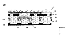
撮像素子100は、被写体側から順に、マイクロレンズ101、カラーフィルタ102、開口マスク103、配線層105および光電変換素子108が配列されて構成されている。光電変換素子108は、入射する光を電気信号に変換するフォトダイオードにより構成される。光電変換素子108は、基板109の表面に二次元的に複数配列されている。
The
光電変換素子108により変換された画像信号、光電変換素子108を制御する制御信号等は、配線層105に設けられた配線106を介して送受信される。また、各光電変換素子108に一対一に対応して設けられた開口部104を有する開口マスク103が、配線層に接して設けられている。開口部104は、後述するように、対応する光電変換素子108ごとにシフトさせて、相対的な位置が厳密に定められている。詳しくは後述するが、この開口部104を備える開口マスク103の作用により、光電変換素子108が受光する被写体光束に視差が生じる。
An image signal converted by the
一方、視差を生じさせない光電変換素子108上には、開口マスク103が存在しない。別言すれば、対応する光電変換素子108に対して入射する被写体光束を制限しない、つまり有効光束の全体を通過させる開口部104を有する開口マスク103が設けられているとも言える。視差を生じさせることはないが、実質的には配線106によって形成される開口107が入射する被写体光束を規定するので、配線106を、視差を生じさせない有効光束の全体を通過させる開口マスクと捉えることもできる。開口マスク103は、各光電変換素子108に対応して別個独立に配列しても良いし、カラーフィルタ102の製造プロセスと同様に複数の光電変換素子108に対して一括して形成しても良い。
On the other hand, the
カラーフィルタ102は、開口マスク103上に設けられている。カラーフィルタ102は、各光電変換素子108に対して特定の波長帯域を透過させるように着色された、光電変換素子108のそれぞれに一対一に対応して設けられるフィルタである。カラー画像を出力するには、互いに異なる少なくとも2種類のカラーフィルタが配列されれば良いが、より高画質のカラー画像を取得するには3種類以上のカラーフィルタを配列すると良い。例えば赤色波長帯を透過させる赤フィルタ、緑色波長帯を透過させる緑フィルタ、および青色波長帯を透過させる青フィルタを格子状に配列すると良い。具体的な配列については後述する。
The
マイクロレンズ101は、カラーフィルタ102上に設けられている。マイクロレンズ101は、入射する被写体光束のより多くを光電変換素子108へ導くための集光レンズである。マイクロレンズ101は、光電変換素子108のそれぞれに一対一に対応して設けられている。マイクロレンズ101は、撮影レンズ20の瞳中心と光電変換素子108の相対的な位置関係を考慮して、より多くの被写体光束が光電変換素子108に導かれるようにその光軸がシフトされていることが好ましい。さらには、開口マスク103の開口部104の位置と共に、後述の特定の被写体光束がより多く入射するように配置位置が調整されても良い。
The
このように、各々の光電変換素子108に対応して一対一に設けられる開口マスク103、カラーフィルタ102およびマイクロレンズ101の一単位を画素と呼ぶ。特に、視差を生じさせる開口マスク103が設けられた画素を視差画素、視差を生じさせる開口マスク103が設けられていない画素を視差なし画素と呼ぶ。例えば、撮像素子100の有効画素領域が24mm×16mm程度の場合、画素数は1200万程度に及ぶ。
As described above, one unit of the
なお、集光効率、光電変換効率が良いイメージセンサの場合は、マイクロレンズ101を設けなくても良い。また、白黒画像信号を出力すれば良い場合にはカラーフィルタ102は設けない。また、裏面照射型イメージセンサの場合は、配線層105が光電変換素子108とは反対側に設けられる。また、開口マスク103の開口部104に色成分を持たせれば、カラーフィルタ102と開口マスク103を一体的に形成することもできる。
Note that in the case of an image sensor with good light collection efficiency and photoelectric conversion efficiency, the
次に、開口マスク103の開口部104と、生じる視差の関係について説明する。図3は、撮像素子100の一部を拡大した様子を表す概略図である。ここでは、説明を簡単にすべく、カラーフィルタ102の配色については後に言及を再開するまで考慮しない。撮像素子100がカラーフィルタ102を備えない場合は、モノクロイメージセンサとしてモノクロの視差画像を生成することができる。また、カラーフィルタ102の配色に言及しない以下の説明においては、同色のカラーフィルタ102を有する視差画素のみを寄せ集めたイメージセンサであると捉えることができる。したがって、以下に説明する繰り返しパターンは、同色のカラーフィルタ102における隣接画素として考えても良い。
Next, the relationship between the opening 104 of the
図3に示すように、開口マスク103の開口部104は、それぞれの画素に対して相対的にシフトして設けられている。そして、隣接する画素同士においても、それぞれの開口部104は互いに変位した位置に設けられている。
As shown in FIG. 3, the
図の例においては、それぞれの画素に対する開口部104の位置として、互いに左右方向にシフトした6種類の開口マスク103が用意されている。そして、撮像素子100の全体は、紙面左側から右側へ徐々にシフトする開口マスク103をそれぞれ有する6つの視差画素を一組とする光電変換素子群が、二次元的かつ周期的に配列されている。つまり、撮像素子100は、一組の光電変換素子群を含む繰り返しパターン110が、周期的かつ連続的に敷き詰められて構成されていると言える。しかしながら、繰り返しパターン110は、2次元方向の少なくとも一方向に連続的に敷き詰められていればよく、他方向に非連続であってもよい。また、撮像素子100は、実質的に視差画像を生成できる範囲内において、一部に繰り返しパターン110が省かれた部分を有してもよい。実質的に視差画像を生成できる範囲とは、例えば、像としての齟齬が生じないよう補間できる範囲である。また、繰り返しパターン110が省かれた部分が、視覚的に影響を与えない周辺領域である場合も、実質的に視差画像を生成できる。
In the example shown in the drawing, six types of opening
図4は、視差画素と被写体の関係を説明する概念図である。特に図4(a)は撮像素子100のうち撮影光軸21と直交する中心に配列されている繰り返しパターン110tの光電変換素子群を示し、図4(b)は周辺部分に配列されている繰り返しパターン110uの光電変換素子群を模式的に示している。図4(a)、(b)における被写体30は、撮影レンズ20に対して合焦位置に存在する。図4(c)は、図4(a)に対応して、撮影レンズ20に対して非合焦位置に存在する被写体31を捉えた場合の関係を模式的に示している。
FIG. 4 is a conceptual diagram illustrating the relationship between the parallax pixels and the subject. In particular, FIG. 4A shows a photoelectric conversion element group of a repetitive pattern 110t arranged in the center orthogonal to the photographing
まず、撮影レンズ20が合焦状態に存在する被写体30を捉えている場合の、視差画素と被写体の関係を説明する。被写体光束は、撮影レンズ20の瞳を通過して撮像素子100へ導かれるが、被写体光束が通過する全体の断面領域に対して、6つの部分領域Pa〜Pfが規定されている。そして、例えば繰り返しパターン110t、110uを構成する光電変換素子群の紙面左端の画素は、拡大図からもわかるように、部分領域Pfから射出された被写体光束のみが光電変換素子108へ到達するように、開口マスク103の開口部104fの位置が定められている。同様に、右端の画素に向かって、部分領域Peに対応して開口部104eの位置が、部分領域Pdに対応して開口部104dの位置が、部分領域Pcに対応して開口部104cの位置が、部分領域Pbに対応して開口部104bの位置が、部分領域Paに対応して開口部104aの位置がそれぞれ定められている。
First, the relationship between the parallax pixels and the subject when the photographing
別言すれば、例えば部分領域Pfと左端画素の相対的な位置関係によって定義される、部分領域Pfから射出される被写体光束の主光線Rfの傾きにより、開口部104fの位置が定められていると言っても良い。そして、合焦位置に存在する被写体30からの被写体光束を、開口部104fを介して光電変換素子108が受光する場合、その被写体光束は、点線で図示するように、光電変換素子108上で結像する。同様に、右端の画素に向かって、主光線Reの傾きにより開口部104eの位置が、主光線Rdの傾きにより開口部104dの位置が、主光線Rcの傾きにより開口部104cの位置が、主光線Rbの傾きにより開口部104bの位置が、主光線Raの傾きにより開口部104aの位置がそれぞれ定められていると言える。
In other words, the position of the
図4(a)で示すように、合焦位置に存在する被写体30のうち、光軸21と交差する被写体30上の微小領域Otから放射される光束は、撮影レンズ20の瞳を通過して、繰り返しパターン110tを構成する光電変換素子群の各画素に到達する。すなわち、繰り返しパターン110tを構成する光電変換素子群の各画素は、それぞれ6つの部分領域Pa〜Pfを介して、一つの微小領域Otから放射される光束を受光している。微小領域Otは、繰り返しパターン110tを構成する光電変換素子群の各画素の位置ずれに対応する分だけの広がりを有するが、実質的には、ほぼ同一の物点と近似することができる。同様に、図4(b)で示すように、合焦位置に存在する被写体30のうち、光軸21から離間した被写体30上の微小領域Ouから放射される光束は、撮影レンズ20の瞳を通過して、繰り返しパターン110uを構成する光電変換素子群の各画素に到達する。すなわち、繰り返しパターン110uを構成する光電変換素子群の各画素は、それぞれ6つの部分領域Pa〜Pfを介して、一つの微小領域Ouから放射される光束を受光している。微小領域Ouも、微小領域Otと同様に、繰り返しパターン110uを構成する光電変換素子群の各画素の位置ずれに対応する分だけの広がりを有するが、実質的には、ほぼ同一の物点と近似することができる。
As shown in FIG. 4A, the light beam emitted from the minute region Ot on the subject 30 that intersects the
つまり、被写体30が合焦位置に存在する限りは、撮像素子100上における繰り返しパターン110の位置に応じて、光電変換素子群が捉える微小領域が異なり、かつ、光電変換素子群を構成する各画素は互いに異なる部分領域を介して同一の微小領域を捉えている。そして、それぞれの繰り返しパターン110において、対応する画素同士は同じ部分領域からの被写体光束を受光している。つまり、図においては、例えば繰り返しパターン110t、110uのそれぞれの左端の画素は、同じ部分領域Pfからの被写体光束を受光している。
In other words, as long as the subject 30 exists at the in-focus position, the minute area captured by the photoelectric conversion element group differs according to the position of the
撮影光軸21と直交する中心に配列されている繰り返しパターン110tにおいて左端画素が部分領域Pfからの被写体光束を受光する開口部104fの位置と、周辺部分に配列されている繰り返しパターン110uにおいて左端画素が部分領域Pfからの被写体光束を受光する開口部104fの位置は厳密には異なる。しかしながら、機能的な観点からは、部分領域Pfからの被写体光束を受光するための開口マスクという点で、これらを同一種類の開口マスクとして扱うことができる。したがって、図4の例では、撮像素子100上に配列される視差画素のそれぞれは、6種類の開口マスクの一つを備えると言える。
In the repetitive pattern 110t arranged in the center orthogonal to the photographing
次に、撮影レンズ20が非合焦状態に存在する被写体31を捉えている場合の、視差画素と被写体の関係を説明する。この場合も、非合焦位置に存在する被写体31からの被写体光束は、撮影レンズ20の瞳の6つの部分領域Pa〜Pfを通過して、撮像素子100へ到達する。ただし、非合焦位置に存在する被写体31からの被写体光束は、光電変換素子108上ではなく他の位置で結像する。例えば、図4(c)に示すように、被写体31が被写体30よりも撮像素子100に対して遠い位置に存在すると、被写体光束は、光電変換素子108よりも被写体31側で結像する。逆に、被写体31が被写体30よりも撮像素子100に対して近い位置に存在すると、被写体光束は、光電変換素子108よりも被写体31とは反対側で結像する。
Next, the relationship between the parallax pixels and the subject when the photographing
したがって、非合焦位置に存在する被写体31のうち、微小領域Ot'から放射される被写体光束は、6つの部分領域Pa〜Pfのいずれを通過するかにより、異なる組の繰り返しパターン110における対応画素に到達する。例えば、部分領域Pdを通過した被写体光束は、図4(c)の拡大図に示すように、主光線Rd'として、繰り返しパターン110t'に含まれる、開口部104dを有する光電変換素子108へ入射する。そして、微小領域Ot'から放射された被写体光束であっても、他の部分領域を通過した被写体光束は、繰り返しパターン110t'に含まれる光電変換素子108へは入射せず、他の繰り返しパターンにおける対応する開口部を有する光電変換素子108へ入射する。換言すると、繰り返しパターン110t'を構成する各光電変換素子108へ到達する被写体光束は、被写体31の互いに異なる微小領域から放射された被写体光束である。すなわち、開口部104dに対応する108へは主光線をRd'とする被写体光束が入射し、他の開口部に対応する光電変換素子108へは主光線をRa+、Rb+、Rc+、Re+、Rf+とする被写体光束が入射するが、これらの被写体光束は、被写体31の互いに異なる微小領域から放射された被写体光束である。このような関係は、図4(b)における周辺部分に配列されている繰り返しパターン110uにおいても同様である。Therefore, the subject luminous flux emitted from the minute region Ot ′ among the
すると、撮像素子100の全体で見た場合、例えば、開口部104aに対応する光電変換素子108で捉えた被写体像Aと、開口部104dに対応する光電変換素子108で捉えた被写体像Dは、合焦位置に存在する被写体に対する像であれば互いにずれが無く、非合焦位置に存在する被写体に対する像であればずれが生じることになる。そして、そのずれは、非合焦位置に存在する被写体が合焦位置に対してどちら側にどれだけずれているかにより、また、部分領域Paと部分領域Pdの距離により、方向と量が定まる。つまり、被写体像Aと被写体像Dは、互いに視差像となる。この関係は、他の開口部に対しても同様であるので、開口部104aから104fに対応して、6つの視差像が形成されることになる。
Then, when viewed as a whole of the
したがって、このように構成されたそれぞれの繰り返しパターン110において、互いに対応する画素の出力を寄せ集めると、視差画像が得られる。つまり、6つの部分領域Pa〜Pfうちの特定の部分領域から射出された被写体光束を受光した画素の出力は、視差画像を形成する。
Therefore, when the outputs of the pixels corresponding to each other in each of the
図5は、視差画像を生成する処理を説明する概念図である。図は、左列から順に、開口部104fに対応する視差画素の出力を集めて生成される視差画像データIm_fの生成の様子、開口部104eの出力による視差画像データIm_eの生成の様子、開口部104dの出力による視差画像データIm_dの生成の様子、開口部104cの出力による視差画像データIm_cの生成の様子、開口部104bの出力による視差画像データIm_bの生成の様子、開口部104aの出力による視差画像データIm_aの生成の様子を表す。まず開口部104fの出力による視差画像データIm_fの生成の様子について説明する。
FIG. 5 is a conceptual diagram illustrating processing for generating a parallax image. The figure shows, in order from the left column, the generation of the parallax image data Im_f generated by collecting the outputs of the parallax pixels corresponding to the
6つの視差画素を一組とする光電変換素子群から成る繰り返しパターン110は、横一列に配列されている。したがって、開口部104fを有する視差画素は、撮像素子100上において、左右方向に6画素おき、かつ、上下方向に連続して存在する。これら各画素は、上述のようにそれぞれ異なる微小領域からの被写体光束を受光している。したがって、これらの視差画素の出力を寄せ集めて配列すると、視差画像が得られる。
A repeating
しかし、本実施形態における撮像素子100の各画素は正方画素であるので、単に寄せ集めただけでは、横方向の画素数が1/6に間引かれた結果となり、縦長の画像データが生成されてしまう。そこで、補間処理を施して横方向に6倍の画素数とすることにより、本来のアスペクト比の画像として視差画像データIm_fを生成する。ただし、そもそも補間処理前の視差画像データが横方向に1/6に間引かれた画像であるので、横方向の解像度は、縦方向の解像度よりも低下している。つまり、生成される視差画像データの数と、解像度の向上は相反関係にあると言える。
However, since each pixel of the
同様にして、視差画像データIm_e〜視差画像データIm_aが得られる。すなわち、デジタルカメラ10は、横方向に視差を有する6視点の視差画像を生成することができる。
Similarly, parallax image data Im_e to parallax image data Im_a are obtained. That is, the
上記の例では、横一列を繰り返しパターン110として周期的に配列される例を説明したが、繰り返しパターン110はこれに限らない。図6は、繰り返しパターン110の他の例を示す図である。
In the above example, the example in which one horizontal row is periodically arranged as the repeating
図6(a)は、縦6画素を繰り返しパターン110とした例である。ただし、それぞれの開口部104は、紙面上端の視差画素から下に向かって、紙面左側から右側へ徐々にシフトするように位置が定められている。このように配列された繰り返しパターン110によっても、横方向に視差を与える6視点の視差画像を生成することができる。この場合は、図3の繰り返しパターン110に比較すると、縦方向の解像度を犠牲にする代わりに横方向の解像度を維持する繰り返しパターンであると言える。
FIG. 6A shows an example in which the vertical 6 pixels are the repeated
図6(b)は、斜め方向に隣接する6画素を繰り返しパターン110とした例である。それぞれの開口部104は、紙面左上端の視差画素から右下に向かって、紙面左側から右側へ徐々にシフトするように位置が定められている。このように配列された繰り返しパターン110によっても、横方向に視差を与える6視点の視差画像を生成することができる。この場合は、図3の繰り返しパターン110に比較すると、縦方向の解像度および横方向の解像度をある程度維持しつつ、視差画像の数を増やす繰り返しパターンであると言える。
FIG. 6B shows an example in which six pixels adjacent in the oblique direction are used as the repeated
図3の繰り返しパターン110、および図6(a)(b)の繰り返しパターン110をそれぞれ比較すると、いずれも6視点の視差画像を生成する場合において、視差画像でない全体から一枚の画像を出力する場合の解像度に対し、縦方向、横方向のいずれの方向の解像度を犠牲にするかの違いであると言える。図3の繰り返しパターン110の場合は、横方向の解像度を1/6とする構成である。図6(a)の繰り返しパターン110の場合は、縦方向の解像度を1/6とする構成である。また、図6(b)の繰り返しパターン110の場合は、縦方向を1/3、横方向を1/2とする構成である。いずれの場合も、一つのパターン内には、各画素に対応して開口部104a〜104fが一つずつ設けられており、それぞれが対応する部分領域Pa〜Pfのいずれかから被写体光束を受光するように構成されている。したがって、いずれの繰り返しパターン110であっても視差量は同等である。
When the
上述の繰り返しパターン110によれば、解像度と視差数はトレードオフの関係にあるが、次に視差の数を減らさずに解像度を上げる位相ずらし配列の手法について説明する。まずは、前提の構成となる、位相ずらし配列でない構成について説明する。
According to the
図7は、位相ずらし配列でない視差画素と被写体の関係を説明する概念図である。図7で示す繰り返しパターン110によれば、それぞれの視差画素における開口部104a〜104iは、それぞれ撮影レンズ20の瞳における部分領域Pa〜Piからの被写体光束のみを通過させるので、撮像素子100は、9視点の視差画像を出力する。この場合は、9つの視差画素が同一の微小領域から放射される光束を受光するので、9画素がそれぞれ別の微小領域から放射される光束を受光する場合に比べて1/9の解像度となる。例えば、合焦位置に存在する被写体30のうち、微小領域Os3から放射された被写体光束は、9つの部分領域Pa〜Piを通過することにより分割され、像側領域Is3で結像する。像側領域Is3は、開口部104a〜104iを有する一つの繰り返しパターン110に対応する領域である。FIG. 7 is a conceptual diagram illustrating the relationship between a parallax pixel that is not phase-shifted and an object. According to the
同様に、微小領域Os2から放射された被写体光束は、9つの部分領域Pa〜Piを通過して像側領域Is2で結像する。また、微小領域Os1から放射された被写体光束は、9つの部分領域Pa〜Piを通過して像側領域Is1で結像する。像側領域Is2、I s1 も、それぞれ開口部104a〜104iを有する一つの繰り返しパターン110に対応する領域である。つまり、微小領域と繰り返しパターン110が一対一に対応する構成である。したがって、視差画素に配置される開口部104a〜104iは、一つの繰り返しパターン110内で順番に配列されている。図においては、繰り返しパターン110内において、右端視差画素に開口部104aが配置され、左へ向かってb、c…と続き、左端視差画素に開口部104iが配置されている。この配列は、撮像素子100を形成する繰り返しパターン110のいずれにおいても同様である。
Similarly, the subject light beam emitted from the minute area O s2 is imaged in the image side region I s2 through nine partial areas Pa~Pi. Further, the subject luminous flux emitted from the minute area O s1 passes through the nine partial areas Pa to Pi and forms an image in the image side area I s1 . The image side regions I s2 and I s1 are also regions corresponding to one
これに対し、位相ずらし配列は、一つの微小領域から放射された被写体光束のうち、複数の部分領域の全てではなく選択された幾つかの部分領域を通過する光束を受光するように、視差画素を配列して繰り返しパターン110を形成する。図8は、位相ずらし配列における視差画素と被写体の関係を説明する概念図である。図の例の位相ずらし配列は、一つの微小領域から放射された被写体光束のうち、選択された幾つかの部分領域を通過する光束を受光し、かつ、微小領域に対して選択される部分領域が隣り合う微小領域に対して変化するように構成されている。選択される部分領域を固定するパターンもあり得るが、ここでは図の例に即して説明する。
On the other hand, the phase-shifted array receives parallax pixels so as to receive light beams that pass through some selected partial areas, rather than all of the plurality of partial areas, out of the subject light flux emitted from one minute area. Are arranged to form a repeated
図7の配列においては、一つの微小領域から放射される被写体光束に対して、9つの部分領域Pa〜Piを通過する全てを受光すべく9つの視差画素で受光した。一方、図8の位相ずらし配列においては、一つの微小領域から放射される被写体光束に対して、9つの部分領域Pa〜Piのうちの3つを受光すべく3つの視差画素で受光している。このように、部分領域の一部を選択することにより、微小領域の数を増やして解像度を上げている。図の例では、9つのうちの3つを選択することにより、解像度を3倍に上げている。 In the arrangement of FIG. 7, the subject light flux emitted from one minute area is received by nine parallax pixels so as to receive all of the light passing through the nine partial areas Pa to Pi. On the other hand, in the phase-shifted arrangement in FIG. 8, three parallax pixels are used to receive three of the nine partial areas Pa to Pi with respect to the subject luminous flux emitted from one minute area. . Thus, by selecting a part of the partial area, the number of minute areas is increased to increase the resolution. In the example shown in the figure, the resolution is tripled by selecting three of the nine.
具体的な配列としては、図7における繰り返しパターン110を構成する各視差画素のうち、隣接しない3つの視差画素を組として、互い違いに配列しなおした場合に相当する。より具体的には、開口部104a、d、gを有する視差画素を一組、開口部104b、e、hを有する視差画素を一組、開口部104c、f、iを有する視差画素を一組として、互いの組の相対関係が互い違いとなるように組み替える。つまり、それぞれの組を、位相をずらして配列する。図の例では、位相をずらして配列した結果、新たに形成される繰り返しパターン110内において、右端視差画素に開口部104gが配置され、左へ向かって順にe、c、a、h、f、d、bと続き、左端視差画素に開口部104iが配置されている。この配列は、撮像素子100を形成する繰り返しパターン110のいずれにおいても同様である。
A specific arrangement corresponds to a case where, among the parallax pixels constituting the
このように新たに形成された繰り返しパターン110に含まれる視差画素のそれぞれは、合焦位置に存在する被写体30のうち、図7の繰り返しパターン110のように一つの微小領域のみから放射される被写体光束を受光するのではなく、三つの微小領域からそれぞれ放射される被写体光束のいずれかを受光する。例えば、図8の像側領域Ip9近傍の繰り返しパターン110に含まれる各視差画素は、拡大図に示すように、微小領域Op9から放射される被写体光束を、開口部104c、f、iを有する3つの視差画素で受光する。そして、この繰り返しパターン110に含まれる開口部104g、a、dを有する視差画素は別の微小領域からの被写体光束を、開口部104e、h、bを有する視差画素はさらに別の微小領域からの被写体光束をそれぞれ受光する。Each of the parallax pixels included in the newly formed
図9は、繰り返しパターンを説明する図である。図9(a)は、図7に対応する9画素の繰り返しパターン110であり、位相ずらし配列によるパターンではない。この場合、繰り返しパターン110を構成する視差画素は、すべて微小領域Os1から放射された光束を受光している。FIG. 9 is a diagram for explaining a repeating pattern. FIG. 9A shows a
図9(b)は、図8に対応する9画素の繰り返しパターン110であり、位相ずらし配列によるパターンである。この場合、繰り返しパターン110を構成する9つの視差画素は、右から左へ向かって順に開口部104g、e、c、a、h、f、d、b、iを有する開口マスク103を備える光電変換素子群として定義され得る。なお、位相ずらし配列によるパターンでは、それぞれの視差画素が同一の微小領域からの被写体光束を受光するわけではないので、隣接する9画素を一組とすれば、いずれの画素間を区切りに設定しても良い。
FIG. 9B shows a
上述の例では、9視点の視差画像を生成する繰り返しパターン110から、3倍の解像度を得る位相ずらし配列による繰り返しパターン110を作る例を説明した。位相ずらし配列は、他にも様々なバリエーションが存在する。視差画素の配列を幾何学的に組み合わせることにより、視差画像数および解像度等のバランスを考慮しつつ、多種多様の繰り返しパターン110を設定することができる。
In the above-described example, the example has been described in which the
なお、上述の例によれば、図8で示すように、位相ずらし配列に基づく繰り返しパターン110による微小領域の間隔は等間隔である。別言すれば、繰り返しパターン110が隣接して連続すれば、それぞれの視差画素が捉える微小領域は、ある被写体平面において少なくとも一次元方向に等間隔であると言える。微小領域の間隔が等間隔であれば、取得される視差画像に像としての歪みが生じないので、違和感のない視差画像が得られる。
According to the above-described example, as shown in FIG. 8, the intervals between the minute regions by the repeated
上述の例においては、図9(a)のように定義した繰り返しパターン110を、開口部104a、d、gを有する視差画素を一組、開口部104b、e、hを有する視差画素を一組、開口部104c、f、iを有する視差画素を一組として、図9(b)に示す繰り返しパターン110に組み替えた。この場合は、合焦位置に存在する被写体30において微小領域が等間隔になるように視差画素の組を決定している。図8の例では、被写体30においてx方向である一次元方向に等間隔の場合を説明したが、後述のようにy方向にも視差を与えるべく開口部104を変位させる場合にも、y方向も加えた二次元方向に微小領域が等間隔に並ぶように視差画素の組を決定することができる。つまり、選択された視差画素の組のそれぞれが、互い違いに位相をずらして配列された場合に、それぞれの視差画素に対応する微小領域が、x方向、y方向の少なくとも一方において、等間隔に並ぶように組み替えることができる。二次元方向共に位相ずらし配列を採用する場合は、被写体領域によらず解像度が一定となるので、合焦位置に存在する被写体30において微小領域が等間隔に並ぶように組み替えることが好ましい。または、観察者である人間の視覚特性を考慮して、合焦位置に存在する被写体30において少なくとも横方向には微小領域が等間隔に並ぶように組み替えることが好ましい。なお、画像処理等により像としての歪みは解消し得るので、他の制約条件等を優先して、微小領域の間隔が等間隔とならない繰り返しパターン110を採用しても良い。
In the above example, the
上述の例では、主に左右方向に視差を与える視差画像を生成する場合について説明したが、もちろん上下方向に視差を与える視差画像を生成することもできるし、上下左右の二次元方向に視差を与える視差画像を生成することもできる。図10は、二次元的な繰り返しパターン110の例を示す図である。
In the above example, the case of generating a parallax image that gives parallax mainly in the left-right direction has been described, but of course, a parallax image that gives parallax in the vertical direction can also be generated, A parallax image to be given can also be generated. FIG. 10 is a diagram illustrating an example of a two-dimensional
図10の例によれば、縦6画素横6画素の36画素を一組の光電変換素子群として繰り返しパターン110を形成する。それぞれの画素に対する開口部104の位置として、互いに上下左右方向にシフトした36種類の開口マスク103が用意されている。具体的には、各開口部104は、繰り返しパターン110の上端画素から下端画素に向かって、上側から下側へ徐々にシフトすると同時に、左端画素から右端画素に向かって、左側から右側へ徐々にシフトするように位置決めされている。
According to the example of FIG. 10, the
このような繰り返しパターン110を有する撮像素子100は、上下方向および左右方向に視差を与える、36視点の視差画像を出力することができる。もちろん図10の例に限らず、さまざまな視点数の視差画像を出力するように繰り返しパターン110を定めることができる。その場合、上述の位相ずらし配列を2次元配列に応用しても良い。
The
以上の説明においては、開口部104の形状として矩形を採用した。特に、横方向に視差を与える配列においては、シフトさせる方向である左右方向の幅よりも、シフトさせない上下方向の幅を広くすることにより、光電変換素子108へ導く光量を確保している。しかし、開口部104の形状は矩形に限定されない。
In the above description, a rectangle is adopted as the shape of the
図11は、開口部104の他の形状を説明する図である。図においては、開口部104の形状を円形とした。円形とした場合、半球形状であるマイクロレンズ101との相対的な関係から、予定外の被写体光束が迷光となって光電変換素子108へ入射することを防ぐことができる。
FIG. 11 is a diagram for explaining another shape of the
次に、カラーフィルタ102と視差画像について説明する。図12は、ベイヤー配列を説明する図である。図示するように、ベイヤー配列は、緑フィルタが左上と右下の2画素に、赤フィルタが左下の1画素に、青フィルタが右上の1画素に割り当てられる配列である。ここでは、緑フィルタが割り当てられた左上の画素をGb画素と、同じく緑色フィルタが割り当てられた右下の画素をGr画素とする。また、赤色フィルタが割り当てられた画素をR画素と、青色が割り当てられた画素をB画素とする。そして、Gb画素およびB画素が並ぶ横方向をGb行とし、R画素およびGr画素が並ぶ横方向をGr行とする。また、Gb画素およびR画素が並ぶ縦方向をGb列とし、B画素およびGr画素が並ぶ縦方向をGr列とする。
Next, the
このようなカラーフィルタ102の配列に対して、視差画素と視差なし画素を、何色の画素にどのような周期で割り振っていくかにより、膨大な数の繰り返しパターン110が設定され得る。視差なし画素の出力を集めれば、通常の撮影画像と同じく視差のない撮影画像データを生成することができる。したがって、相対的に視差なし画素の割合を増やせば、解像度の高い2D画像を出力させることができる。この場合、視差画素は相対的に少ない割合となるので、複数の視差画像からなる3D画像としては画質が低下する。逆に、視差画素の割合を増やせば、3D画像としては画質が向上するが、視差なし画素は相対的に減少するので、解像度の低い2D画像が出力される。
With respect to such an arrangement of the
このようなトレードオフの関係において、何れの画素を視差画素とするか、あるいは視差なし画素とするかにより、様々な特徴を有する繰り返しパターン110が設定される。図13は、ベイヤー配列に対する視差画素の割り振りについて、視差画素の種類が2つである場合のバリエーションを説明する図である。この場合の視差画素は、開口部104が中心よりも左側に偏心した視差L画素と、同じく右側に偏心した視差R画素を想定している。つまり、このような視差画素から出力される2視点の視差画像は、いわゆる立体視を実現する。
In such a trade-off relationship, a
それぞれの繰り返しパターンに対する特徴の説明は図に示す通りである。例えば、視差なし画素が多く割り振られていれば高解像度の2D画像データとなり、RGBのいずれの画素に対しても均等に割り振られていれば、色ずれの少ない高画質の2D画像データとなる。視差画素の出力も利用して2D画像データを生成する場合、ずれた被写体像を周辺画素の出力を参照して補正する。したがって、例えば全部のR画素が視差画素であったとしても2D画像を生成することはできるものの、その画質は自ずと低下する。 The description of the features for each repetitive pattern is as shown in the figure. For example, if many non-parallax pixels are allocated, high-resolution 2D image data is obtained, and if all pixels of RGB are equally allocated, high-quality 2D image data with little color shift is obtained. When 2D image data is generated using the output of the parallax pixels, the shifted subject image is corrected with reference to the output of the peripheral pixels. Therefore, for example, even if all R pixels are parallax pixels, a 2D image can be generated, but the image quality is naturally lowered.
一方、視差画素が多く割り振られていれば高解像度の3D画像データとなり、RGBのいずれの画素に対しても均等に割り振られていれば、3D画像でありながら、色再現性の良い高品質のカラー画像データとなる。視差なし画素の出力も利用して3D画像データを生成する場合、視差のない被写体像から周辺の視差画素の出力を参照してずれた被写体像を生成する。したがって、例えば全部のR画素が視差なし画素であったとしてもカラーの3D画像を生成することはできるものの、やはりその品質は低下する。 On the other hand, if a large number of parallax pixels are allocated, high-resolution 3D image data is obtained, and if all the RGB pixels are allocated equally, a high-quality image with good color reproducibility can be obtained while being a 3D image. Color image data. When 3D image data is generated using the output of pixels without parallax, a subject image shifted from a subject image without parallax is generated with reference to the output of peripheral parallax pixels. Therefore, for example, even if all the R pixels are non-parallax pixels, a color 3D image can be generated, but the quality is still deteriorated.
以下にいくつかのバリエーションについて説明する。図14は、バリエーションの一例を示す図である。図14のバリエーションは、図13における繰り返しパターン分類A−1に相当する。 Some variations are described below. FIG. 14 is a diagram illustrating an example of a variation. The variation in FIG. 14 corresponds to the repeated pattern classification A-1 in FIG.
図の例においては、ベイヤー配列と同じ4画素を繰り返しパターン110とする。R画素とG画素は視差なし画素であり、Gb画素を視差L画素に、Gr画素を視差R画素に割り当てる。この場合、同一の繰り返しパターン110に含まれる視差L画素と視差R画素が、被写体が合焦位置に存在するときに、同じ微小領域から放射される光束を受光するように開口部104を定めることもできるし、異なる微小領域から放射される光束を受光するように開口部104を定めることもできる。異なる微小領域から放射される光束を受光するように開口部104を定めた場合、位相ずらし配列として、例えば、左右に隣接する2つの繰り返しパターン110において、左側の繰り返しパターン110のGb画素に割り当てられた視差L画素と、右側の繰り返しパターン110のGr画素に割り当てられた視差R画素とが、同一の微小領域から放射される光束を受光するように構成することができる。
In the example of the figure, the same four pixels as the Bayer array are used as the repeated
図の例においては、視感度の高い緑画素であるGb画素およびGr画素を視差画素として用いるので、コントラストの高い視差画像を得ることが期待できる。また、同じ緑色画素であるGb画素およびGr画素を視差画素として用いるので、これら2つの出力から視差のない出力に変換演算がし易く、視差なし画素であるR画素およびB画素の出力と共に、高画質の2D画像データを生成できる。 In the example of the figure, Gb pixels and Gr pixels, which are green pixels with high visibility, are used as parallax pixels, so that it is expected to obtain a parallax image with high contrast. In addition, since the Gb pixel and the Gr pixel which are the same green pixels are used as the parallax pixels, it is easy to perform a conversion operation from these two outputs to an output having no parallax, and the output of the R pixel and the B pixel which are non-parallax pixels is high. High-quality 2D image data can be generated.
図15は、他のバリエーションの一例を示す図である。図15のバリエーションは、図13における繰り返しパターン分類B−1に相当する。 FIG. 15 is a diagram illustrating an example of another variation. The variation in FIG. 15 corresponds to the repeated pattern classification B-1 in FIG.
図の例においては、ベイヤー配列の4画素が左右に2組続く8画素を繰り返しパターン110とする。8画素のうち、左側のGb画素に視差L画素を、右側のGb画素に視差R画素を割り当てる。このような配列においては、Gr画素を視差なし画素としたことにより、図13の例よりも、更に2D画像の高画質化が望める。
In the example shown in the figure, the repeated
図16は、更に他のバリエーションの一例を示す図である。図16のバリエーションは、図13における繰り返しパターン分類C−1に相当する。 FIG. 16 is a diagram illustrating an example of still another variation. The variation in FIG. 16 corresponds to the repeated pattern classification C-1 in FIG.
図の例においては、ベイヤー配列の4画素が左右に2組続く8画素を繰り返しパターン110とする。8画素のうち、左側のGb画素に視差L画素を、右側のGb画素に視差R画素を割り当てる。さらに、左側のGr画素にも視差L画素を、右側のGr画素にも視差R画素を割り当てる。2つのGb画素に割り当てられた視差L画素と視差R画素は、被写体が合焦位置に存在するときに、一つの微小領域から放射される光束を受光し、2つのGr画素に割り当てられた視差L画素と視差R画素は、Gb画素のそれとは異なる一つの微小領域から放射される光束を受光する。したがって、図15の例に比較して、3D画像としての解像度が縦方向に2倍となる。
In the example shown in the figure, the repeated
図17は、更に他のバリエーションの一例を示す図である。図17のバリエーションは、図13における繰り返しパターン分類D−1に相当する。 FIG. 17 is a diagram illustrating an example of still another variation. The variation in FIG. 17 corresponds to the repeated pattern classification D-1 in FIG.
図の例においては、ベイヤー配列の4画素が左右に2組続く8画素を繰り返しパターン110とする。8画素のうち、左側のGb画素に視差L画素を、右側のGb画素に視差R画素を割り当てる。さらに、左側のR画素に視差L画素を、右側のR画素に視差R画素を割り当てる。さらに、左側のB画素に視差L画素を、右側のB画素に視差R画素を割り当てる。2つのGr画素には視差なし画素を割り当てる。
In the example shown in the figure, the repeated
2つのGb画素に割り当てられた視差L画素と視差R画素は、被写体が合焦位置に存在するときに、一つの微小領域から放射される光束を受光する。また、2つのR画素に割り当てられた視差L画素と視差R画素は、Gb画素のそれとは異なる一つの微小領域から放射される光束を受光し、2つのB画素に割り当てられた視差L画素と視差R画素は、Gb画素およびR画素のそれとは異なる一つの微小領域から放射される光束を受光する。したがって、図15の例に比較して、3D画像としての解像度が縦方向に3倍となる。しかも、RGBの3色の出力が得られるので、カラー画像としての3D画像として高品質である。 The parallax L pixel and the parallax R pixel assigned to the two Gb pixels receive the light beam emitted from one minute region when the subject is in the in-focus position. In addition, the parallax L pixel and the parallax R pixel assigned to the two R pixels receive a light beam emitted from one minute region different from that of the Gb pixel, and the parallax L pixel assigned to the two B pixels The parallax R pixel receives a light beam emitted from one minute region different from that of the Gb pixel and the R pixel. Therefore, compared with the example of FIG. 15, the resolution as a 3D image is tripled in the vertical direction. Moreover, since RGB three-color output can be obtained, it is a high-quality 3D image as a color image.
図18は、ベイヤー配列に対する視差画素の割り振りについて、視差画素の種類が3つである場合のバリエーションを説明する図である。この場合の視差画素は、開口部104が中心よりも左側に偏心した視差L画素、偏心のない視差C画素および右側に偏心した視差R画素を想定している。偏心のない視差C画素は、瞳の中心部分を部分領域とする被写体光束のみを光電変換素子108へ導く点で視差画像を出力する視差画素であり、光電変換素子108に対して入射する被写体光束を制限しない視差なし画素とは異なる。したがって、これら3種類の視差画素により、3視点の視差画像が出力される。
FIG. 18 is a diagram illustrating a variation in the case where there are three types of parallax pixels with respect to the allocation of parallax pixels to the Bayer array. The parallax pixels in this case are assumed to be a parallax L pixel decentered to the left of the
それぞれの繰り返しパターンに対する特徴の説明は図に示す通りである。2視点における2D画像と3D画像のトレードオフの関係は、3視点においても同様である。 The description of the features for each repetitive pattern is as shown in the figure. The trade-off relationship between 2D images and 3D images at two viewpoints is the same at three viewpoints.
3視点におけるバリエーションの一例を説明する。図19は、バリエーションの一例として、図18における繰り返しパターン分類Bt−2に相当する図である。 An example of variations in three viewpoints will be described. FIG. 19 is a diagram corresponding to the repeated pattern classification Bt-2 in FIG. 18 as an example of a variation.
図の例においては、ベイヤー配列の4画素が左右方向に3組続く12画素を繰り返しパターン110とする。12画素のうち、3つのGb画素にそれぞれ左右方向に対応させて視差L画素、視差C画素および視差R画素を割り当てる。他の画素には、全て視差なし画素を割り当てる。
In the example shown in the figure, the repeating
このような繰り返しパターン110によれば、2D画像としての解像度、カラー品質を高いレベルで維持しつつ、3視点の視差画像も同時に取得することができる。
According to such a
図20は、ベイヤー配列に対する視差画素の割り振りについて、視差画素の種類が4つ以上である場合のバリエーションの一例を説明する図である。このように、視点数が増えていっても、さまざまな繰り返しパターン110を形成することができる。したがって、仕様、目的等に応じた繰り返しパターン110を選択することができる。
FIG. 20 is a diagram illustrating an example of a variation in the case where there are four or more types of parallax pixels with respect to the allocation of parallax pixels to the Bayer array. Thus, even if the number of viewpoints is increased, various
上述の例では、カラーフィルタ配列としてベイヤー配列を採用した場合について説明したが、もちろん他のカラーフィルタ配列であっても差し支えない。図3等を用いて説明したように、カラーフィルタ配列を構成するある1色に着目して寄せ集めた場合に、隣接する複数の画素を一組の光電変換素子群とする繰り返しパターンを形成し、視差画像を出力するように視差画素が割り当てられていれば良い。このとき、一組の光電変換素子群を構成する視差画素のそれぞれは、互いに異なる部分領域を向く開口部104を有する開口マスク103を備えると良い。
In the above-described example, the case where the Bayer array is adopted as the color filter array has been described. Of course, other color filter arrays may be used. As described with reference to FIG. 3 and the like, a repetitive pattern in which a plurality of adjacent pixels are set as a set of photoelectric conversion elements is formed when focusing on one color constituting the color filter array. The parallax pixels need only be assigned so as to output a parallax image. At this time, each of the parallax pixels constituting the set of photoelectric conversion element groups may include an
図21は、他のカラーフィルタ配列を説明する図である。図示するように、他のカラーフィルタ配列は、緑フィルタが左上および右上の2画素に、赤フィルタが左下の1画素に、青フィルタが右下の1画素に割り当てられる配列である。ここでは、緑フィルタが割り当てられた左上の画素をGr画素と、同じく緑色フィルタが割り当てられた右上の画素をGb画素とする。また、赤色フィルタが割り当てられた画素をR画素と、青色が割り当てられた画素をB画素とする。そして、Gr画素およびGb画素が並ぶ横方向をG行とし、R画素およびB画素が並ぶ横方向をRB行とする。また、Gr画素およびR画素が並ぶ縦方向をGr列とし、Gb画素およびB画素が並ぶ縦方向をGb列とする。 FIG. 21 is a diagram for explaining another color filter arrangement. As shown in the drawing, the other color filter array is an array in which the green filter is assigned to the upper left and upper right two pixels, the red filter is assigned to the lower left pixel, and the blue filter is assigned to the lower right pixel. Here, the upper left pixel to which the green filter is assigned is the Gr pixel, and the upper right pixel to which the green filter is assigned is the Gb pixel. In addition, a pixel to which a red filter is assigned is an R pixel, and a pixel to which blue is assigned is a B pixel. The horizontal direction in which Gr pixels and Gb pixels are arranged is defined as G row, and the horizontal direction in which R pixels and B pixels are aligned is defined as RB row. The vertical direction in which Gr pixels and R pixels are arranged is referred to as Gr column, and the vertical direction in which Gb pixels and B pixels are arranged is referred to as Gb column.
ベイヤー配列の場合と同じく、このような他のカラーフィルタ配列の場合であっても、視差画素と視差なし画素を、何色の画素にどのような周期で割り振っていくかにより、膨大な数の繰り返しパターン110が設定され得る。また、相対的に視差なし画素の割合を増やせば、解像度の高い2D画像を出力させることができ、視差画素の割合を増やせば、3D画像の画質を向上させることができる関係も同様である。
As in the case of the Bayer array, even in the case of such other color filter arrays, an enormous number of pixels may be used depending on how many colors of pixels the disparity pixels and non-parallax pixels are allocated. A repeating
図22は、他のカラーフィルタ配列に対する視差画素の割り振りについて、視差画素の種類が2つである場合のバリエーションを説明する図である。それぞれの繰り返しパターンに対する特徴の説明は図に示す通りである。例えば、視差なし画素が多く割り振られていれば高解像度の2D画像データとなり、RGBのいずれの画素に対しても均等に割り振られていれば、色ずれの少ない高画質の2D画像データとなる。視差画素の出力も利用して2D画像データを生成する場合、ずれた被写体像を周辺画素の出力を参照して補正する。したがって、例えば全部のR画素が視差画素であったとしても2D画像を生成することはできるものの、その画質は自ずと低下する。 FIG. 22 is a diagram illustrating a variation in the case where there are two types of parallax pixels with respect to allocation of parallax pixels to other color filter arrays. The description of the features for each repetitive pattern is as shown in the figure. For example, if many non-parallax pixels are allocated, high-resolution 2D image data is obtained, and if all pixels of RGB are equally allocated, high-quality 2D image data with little color shift is obtained. When 2D image data is generated using the output of the parallax pixels, the shifted subject image is corrected with reference to the output of the peripheral pixels. Therefore, for example, even if all R pixels are parallax pixels, a 2D image can be generated, but the image quality is naturally lowered.
一方、視差画素が多く割り振られていれば高解像度の3D画像データとなり、RGBのいずれの画素に対しても均等に割り振られていれば、3D画像でありながら、色再現性の良い高品質のカラー画像データとなる。視差なし画素の出力も利用して3D画像データを生成する場合、視差のない被写体像から周辺の視差画素の出力を参照してずれた被写体像を生成する。したがって、例えば全部のR画素が視差なし画素であったとしてもカラーの3D画像を生成することはできるものの、やはりその品質は低下する。 On the other hand, if a large number of parallax pixels are allocated, high-resolution 3D image data is obtained, and if all the RGB pixels are allocated equally, a high-quality image with good color reproducibility can be obtained while being a 3D image. Color image data. When 3D image data is generated using the output of pixels without parallax, a subject image shifted from a subject image without parallax is generated with reference to the output of peripheral parallax pixels. Therefore, for example, even if all the R pixels are non-parallax pixels, a color 3D image can be generated, but the quality is still deteriorated.
図23は、他のカラーフィルタ配列に対する視差画素の割り振りについて、視差画素の種類が3つである場合のバリエーションを説明する図である。この場合の視差画素は、開口部104が中心よりも左側に偏心した視差L画素、偏心のない視差C画素および右側に偏心した視差R画素を想定している。
FIG. 23 is a diagram illustrating a variation in the case where there are three types of parallax pixels with respect to allocation of parallax pixels to other color filter arrays. The parallax pixels in this case are assumed to be a parallax L pixel decentered to the left of the
それぞれの繰り返しパターンに対する特徴の説明は図に示す通りである。2視点における2D画像と3D画像のトレードオフの関係は、3視点においても同様である。 The description of the features for each repetitive pattern is as shown in the figure. The trade-off relationship between 2D images and 3D images at two viewpoints is the same at three viewpoints.
図示は省くが、視差画素の種類が4つ以上であっても、さまざまな繰り返しパターン110を形成することができる。したがって、仕様、目的等に応じた繰り返しパターン110を選択することができる。
Although illustration is omitted, various
図24は、本発明の実施形態に係る他の撮像素子の断面を表す概略図である。図2では、カラーフィルタ102と開口マスク103が別体で構成される撮像素子100の断面概略図を示したが、図24では、撮像素子100の変形例として、カラーフィルタ部122と開口マスク部123が一体的に構成されたスクリーンフィルタ121を備える撮像素子120の断面外略図を示す。
FIG. 24 is a schematic diagram illustrating a cross section of another image sensor according to the embodiment of the present invention. 2 shows a schematic cross-sectional view of the
輝度情報を取得する画素を視差画素とする場合、つまり、視差画像をモノクロ画像として出力するのであれば、図24で示す撮像素子120の構成を採用し得る。すなわち、カラーフィルタとして機能するカラーフィルタ部122と、開口部104を有する開口マスク部123とが一体的に構成されたスクリーンフィルタ121を、マイクロレンズ101と配線層105の間に配設することができる。
When the pixel for obtaining the luminance information is a parallax pixel, that is, when the parallax image is output as a monochrome image, the configuration of the
スクリーンフィルタ121は、カラーフィルタ部122において例えば青緑赤の着色が施され、開口マスク部123において開口部104以外のマスク部分が黒の着色が施されて形成される。スクリーンフィルタ121を採用する撮像素子120は、撮像素子100に比較して、マイクロレンズ101から光電変換素子108までの距離が短いので、被写体光束の集光効率が高い。
The
図25は、他のカラーフィルタ配列を説明する図である。図示するように、他のカラーフィルタ配列は、図12で示したベイヤー配列のGr画素を緑フィルタが割り当てられるG画素として維持する一方、Gb画素をカラーフィルタが割り当てられないW画素に変更した配列である。なお、W画素は、上述のように、可視光のおよそ全ての波長帯域を透過させるように、着色を施さない透明フィルタが配列されていても良い。 FIG. 25 is a diagram for explaining another color filter arrangement. As shown in the figure, the other color filter array maintains the Gr pixels in the Bayer array shown in FIG. 12 as G pixels to which the green filter is assigned, while changing the Gb pixels to W pixels to which no color filter is assigned. It is. Note that, as described above, the W pixel may be arranged with a transparent filter that is not colored so as to transmit substantially all the wavelength band of visible light.
このようなW画素を含むカラーフィルタ配列を採用すれば、撮像素子が出力するカラー情報の精度は若干低下するものの、W画素が受光する光量はカラーフィルタが設けられている場合に比較して多いので、精度の高い輝度情報を取得できる。W画素の出力を寄せ集めれば、モノクロ画像を形成することもできる。 If such a color filter array including W pixels is adopted, the accuracy of the color information output from the image sensor is slightly reduced, but the amount of light received by the W pixels is larger than that when a color filter is provided. Therefore, highly accurate luminance information can be acquired. A monochrome image can also be formed by gathering the outputs of W pixels.
W画素を含むカラーフィルタ配列の場合、視差画素と視差なし画素の繰り返しパターン110は、さらなるバリエーションが存在する。例えば、比較的暗い環境下で撮影された画像であっても、カラー画素から出力された画像に比較してW画素から出力された画像であれば、被写体像のコントラストが高い。そこで、W画素に視差画素を割り振れば、複数の視差画像間で行うマッチング処理において、精度の高い演算結果が期待できる。マッチング処理は、画像データに写り込む被写体像の距離情報を取得する処理の一環として実行される。したがって、2D画像の解像度および視差画像の画質への影響に加え、抽出される他の情報への利害得失も考慮して、視差画素と視差なし画素の繰り返しパターン110が設定される。
In the case of a color filter array including W pixels, there are further variations in the
図26は、図25の他のカラーフィルタ配列を採用する場合の、W画素と視差画素の配列の一例を示す図である。図26のバリエーションは、ベイヤー配列における図15の繰り返しパターン分類B−1に類似するので、ここではB'−1とする。図の例においては、他のカラーフィルタ配列の4画素が左右に2組続く8画素を繰り返しパターン110とする。8画素のうち、左側のW画素に視差L画素を、右側のW画素に視差R画素を割り当てる。このような配列において撮像素子100は、視差画像をモノクロ画像として出力し、2D画像をカラー画像として出力する。
FIG. 26 is a diagram illustrating an example of an array of W pixels and parallax pixels when another color filter array of FIG. 25 is employed. The variation in FIG. 26 is similar to the repeated pattern classification B-1 in FIG. In the example shown in the figure, the repeated
この場合、撮像素子100は、入射光を電気信号に光電変換する、二次元的に配列された光電変換素子108と、光電変換素子108の少なくとも一部のそれぞれに一対一に対応して設けられた開口マスク103と、光電変換素子108の少なくとも一部のそれぞれに一対一に対応して設けられたカラーフィルタ102とを有し、隣接するn個(nは4以上の整数)の光電変換素子108のうち、少なくとも2つに対応して設けられたそれぞれの開口マスク103の開口部104は、互いに異なる波長帯域を透過させる少なくとも2種類のカラーフィルタ102から構成されるカラーフィルタパターンの一パターン内には含まれず、かつ、入射光の断面領域内の互いに異なる部分領域からの光束をそれぞれ通過させるように位置づけられ、n個の光電変換素子108を一組とする光電変換素子群が周期的かつ連続的に配列されていれば良い。
In this case, the
ここで、モノクロ画像としての視差画像の生成と、カラー画像としての2D画像の生成について説明する。 Here, generation of a parallax image as a monochrome image and generation of a 2D image as a color image will be described.
図27は、視差画像と2D画像の生成過程を示す概念図である。図示するように、視差L画素の出力が、撮像素子100上の相対的な位置関係を維持しながら寄せ集められて、L画像データが生成される。一つの繰り返しパターン110に含まれる視差L画素は一つであるので、L画像データを形成する各視差L画素は、それぞれ異なる繰り返しパターン110から寄せ集められていると言える。すなわち、寄せ集められたそれぞれの視差L画素の出力は、被写体の互いに異なる微小領域から放射された光が光電変換された結果であるので、L画像データは、特定の視点(L視点)から被写体を捉えた一つの視差画像データとなる。そして、視差L画素は、W画素に割り振られているので、L画像データは、カラー情報を持たず、モノクロ画像として生成される。
FIG. 27 is a conceptual diagram illustrating a process of generating a parallax image and a 2D image. As shown in the figure, the outputs of the parallax L pixels are gathered together while maintaining the relative positional relationship on the
同様に、視差R画素の出力が、撮像素子100上の相対的な位置関係を維持しながら寄せ集められて、R画像データが生成される。寄せ集められたそれぞれの視差R画素の出力は、被写体の互いに異なる微小領域から放射された光が光電変換された結果であるので、R画像データは、特定の視点(R視点)から被写体を捉えた一つの視差画像データとなる。そして、視差R画素は、W画素に割り振られているので、R画像データは、カラー情報を持たず、モノクロ画像として生成される。
Similarly, the outputs of the parallax R pixels are gathered together while maintaining the relative positional relationship on the
被写体が合焦位置に存在するときに、一つの繰り返しパターン110において、L画素とR画素は、被写体の同一の微小領域から放射される光束を受光する。また、被写体が非合焦位置に存在するときに、一つの繰り返しパターン110において、L画素とR画素は、被写体の互いにずれた微小領域から放射される光束を受光する。そのずれは、被写体位置の合焦位置に対する相対関係と瞳の部分領域の関係とから、方向と量が定まる。したがって、L画像データとR画像データのそれぞれにおいて、視差L画素と視差R画素が撮像素子100上の相対的な位置関係を維持しながら寄せ集められていれば、それぞれが視差画像を形成する。
When the subject exists at the in-focus position, in one
また、視差なし画素の出力が、撮像素子100上の相対的な位置関係を維持しながら寄せ集められて、2D画像データが生成される。このとき、W画素は視差画素であるので、視差なし画素のみで構成されるベイヤー配列からの出力に対して、Gb画素の出力に相当する出力が欠落する。そこで、例えば、この欠落した出力の値として、G画素の出力値を代入する。つまり、G画素の出力で補間処理を行う。このように、補間処理を施せば、ベイヤー配列の出力に対する画像処理を採用して2D画像データを生成することができる。
Further, the outputs of pixels without parallax are gathered together while maintaining the relative positional relationship on the
なお、以上の画像処理は、画像処理部205によって実行される。画像処理部205は、制御部201を介して撮像素子100から出力される画像信号を受け取り、上述のようにそれぞれの画素の出力ごとに分配してL画像データ、R画像データおよび2D画像データを生成する。
Note that the above image processing is executed by the
以上の実施形態においては、撮像素子100は、一組の光電変換素子群を含む繰り返しパターン110が、周期的かつ連続的に敷き詰められて構成されていると説明した。しかし、カラーフィルタを備える視差画素のそれぞれが被写体の離散的な微小領域を捉えて視差画像を出力すれば良いので、例えば、周期的な繰り返しパターン110の間に視差なし画素が連続していても良い。つまり、視差画素を含む繰り返しパターン110は、連続していなくても、周期的であれば視差画像を出力し得る。なお、本実施形態では、マイクロレンズ101が光電変換素子108のそれぞれに一対一に対応して設けられていると説明したが、複数の光電変換素子108に対して一つのマイクロレンズ101が設けられてもよい。この場合、一組の光電変換素子群を含む繰り返しパターン110に対して一つのマイクロレンズ101が設けられてもよいし、繰り返しパターン110に関係なくマイクロレンズが設けられてもよい。
In the above embodiment, it has been described that the
撮像素子の構成を変えた他の実施形態について説明する。図28は、撮像素子の縦断面図である。図28に示すように、撮像素子16は、基板40と、複数の光電変換素子42と、絶縁層44と、配線層46と、配線層48と、開口マスク50aから50fと、導波路56aから56fと、複数のカラーフィルタ62と、マイクロレンズ64とを備えている。尚、配線層46は、第1金属層の一例である。配線層48は、第2金属層の一例である。開口マスク50aから50fは、第3金属層の一例である。図28の例においては、6種類の開口マスク50aから50fおよびそれらに対応して6種類の導波路56aから56fが示されている。
Another embodiment in which the configuration of the image sensor is changed will be described. FIG. 28 is a longitudinal sectional view of the image sensor. As shown in FIG. 28, the
基板40は、シリコン、GaAs等の半導体材料、または、サファイア等の絶縁材料によって構成される。
The
光電変換素子42は、受光した光に対応する電気的な信号を出力する。光電変換素子42は、基板40の上面部に形成されている。光電変換素子42は、フォトダイオード等を適用することができる。光電変換素子42は、X方向及びY方向において一定の間隔を開けて、2次元状に配列されている。
The
絶縁層44は、光電変換素子42、配線層46及び配線層48を互いに絶縁する。絶縁層44は、基板40及び光電変換素子42を覆うように形成されている。絶縁層44は、酸化シリコン、窒化シリコン等の絶縁材料によって構成されている。
The insulating
配線層46及び配線層48は、絶縁層44の内部に埋め込まれている。配線層48は、一定の間隔を空けて、配線層46の上方に積層されている。配線層46及び配線層48は、金属等の導電性材料によって構成される。配線層46及び配線層48は、光電変換素子42から出力された電気信号を伝達する。
The
開口マスク50aから50fは、一定の間隔を空けて、配線層46の上方に積層されている。開口マスク50aから50fは、絶縁層44上に配置されている。これにより、配線層46、配線層48及び開口マスク50aから50fは、光電変換素子42の側から絶縁層44を介してこの順に積層される。開口マスク50aから50fは、金属等の可視光を遮光可能な材料からなる。開口マスク50aから50fは、光電変換素子42のそれぞれに一対一に対応して設けられている。開口マスク50aから50fには、それぞれ開口66aから66fが形成されている。開口66aから66fの位置等については後述する。
The opening masks 50a to 50f are stacked above the
導波路56aから56fは、絶縁層44の内部に形成されている。導波路56aから56fの入射側の端部は、それぞれ開口マスク50aから50fから延びる。導波路56aから56fの他方の端部は、光電変換素子42まで延びる。これにより、導波路56aから56fは、それぞれ開口66aから66fと光電変換素子42とを繋ぐ。導波路56aから56fの構造および機能については後述する。
The
カラーフィルタ62は、例えば、メタクリル酸エステル等の材料からなる。カラーフィルタ62は、開口マスク50aから50f上、及び、開口66aから66fから露出した絶縁層44上に形成されている。カラーフィルタ62は、光電変換素子42のそれぞれに一対一に対応して設けられている。カラーフィルタ62は、各光電変換素子42に対して特定の波長帯域の光を透過させるように着色されている。カラー画像を撮像するには、互いに異なる少なくとも2種類のカラーフィルタ62を配列する。更に高画質のカラー画像を撮像するには、3種類以上のカラーフィルタ62を配列する必要がある。カラーフィルタ62の組み合わせの一例は、赤色波長帯域を透過させる赤色フィルタ、緑色波長帯域を透過させる緑色フィルタ、青色波長帯域を透過させる青色フィルタの組み合わせである。これらのカラーフィルタ62の組み合わせを周期的に配列して、1つのカラーフィルタパターンが形成される。尚、白黒画像信号を出力する場合、カラーフィルタ62は省略してもよい。
The
マイクロレンズ64は、カラーフィルタ62上に形成されている。マイクロレンズ64は、入射する被写体光束をより多く光電変換素子42へと導くための集光レンズである。マイクロレンズ64は、複数の光電変換素子42のそれぞれに一対一に対応して設けられている。マイクロレンズ64は、撮影レンズ20の瞳中心と光電変換素子42の相対的な位置関係を考慮して、より多くの被写体光束が光電変換素子42に導かれるようにその光軸21がシフトされていることが好ましい。尚、集光効率、光電変換効率がよい撮像素子16の場合、マイクロレンズ64は省略してもよい。
The
各々の光電変換素子42に対応して一対一に設けられる開口マスク50aから50f、導波路56aから56f、カラーフィルタ62、マイクロレンズ64の一単位を画素と呼ぶ。特に、視差を生じさせる開口66aから66fが形成された開口マスク50aから50fを含む画素を視差画素、視差を生じさせない開口が形成された開口マスクを含む視差なし画素と呼ぶ。例えば、撮像素子16の有効画素領域が24mm×16mmの場合、画素数は1200万程度に及ぶ。
One unit of the opening masks 50a to 50f, the
この撮像素子16では、撮影レンズ20の光軸21に沿って、被写体光束が入射すると、マイクロレンズ64によって、集光された後、カラーフィルタ62に入射する。光は、カラーフィルタ62によって特定の波長帯域のみが選択的に透過される。その後、特定の方向から入射した光が開口マスク50aから50fの開口66aから66fを通過する。光は、導波路56aから56fの外周壁部74aから74fによって反射されつつ、瞳分割光として光電変換素子42に入射して、電気信号に変換される。
In the
図29、図30、図31、図32、図33は、撮像素子の製造方法を説明する図である。尚、図31は、図30の溝周辺の拡大図である。図29に示すように、基板40に光電変換素子42が形成される。次に、配線層46の下層まで、スピンコート法等により絶縁層44aが、基板40及び光電変換素子42の上面全体に形成される。リフトオフ法等によりパターニングされた配線層46が、絶縁層44aの上面に形成される。スピンコート法等により絶縁層44bが配線層46及び絶縁層44aの上面全体に形成される。リフトオフ法等によりパターニングされた配線層48が、絶縁層44bの上面に形成される。次に、スピンコート法等により絶縁層44cが、配線層48及び絶縁層44bの上面全体に形成される。尚、絶縁層44a、44b、44cによって、絶縁層44が構成される。
29, 30, 31, 32, and 33 are diagrams for describing a method of manufacturing an image sensor. FIG. 31 is an enlarged view around the groove of FIG. As shown in FIG. 29, the
次に、図30に示すように、ドライエッチング等の異方性エッチングにより、導波路56aから56fの外周壁部74aから74fに対応する領域の絶縁層44を除去して溝80を形成する。ここで、導波路56a等の半径方向において、溝80は、外周壁部74a等よりも厚い。溝80を形成した後に、図31に示すように、絶縁層44の除去された溝80に絶縁材料を埋め込む。これにより、埋め込まれた絶縁材料の内部に空気が残り、図30に示すように、空気が充填された外周壁部74aから74fが形成される。
Next, as shown in FIG. 30, the
次に、図32に示すように、リフトオフ法等によって、パターニングされた複数の開口マスク50aから50fが絶縁層44上に形成される。それぞれの開口マスク50aから50fの開口66aから66fは、導波路56aから56fの上端の位置および大きさに合わせて形成される。
Next, as shown in FIG. 32, a plurality of patterned opening masks 50a to 50f are formed on the insulating
図33に示すように、カラーフィルタ62が、開口マスク50aから50fの上面に形成される。尚、カラーフィルタ62は、開口マスク50aから50fの上面に材料が塗布された後、対応する各領域の色に現像されて形成される。この後、カラーフィルタ62の上面にマイクロレンズ64が形成されて、図28に示す撮像素子16が完成する。
As shown in FIG. 33, the
さらに図28を用いて導波路56a等の構成および作用を説明する。上記の通り、導波路56aから56fの−Z側の端部の開口は、それぞれ開口マスク50aから50fの開口66aから66fと略同じ位置および略同じ大きさに形成されている。導波路56aから56fの下端の中心は、光電変換素子42の中心と一致させている。
Further, the configuration and operation of the
導波路56aから56fはそれぞれ、外周壁部74aから74fを有する。外周壁部74a等は、それぞれ導波路56a等の外周を囲むように形成されている。外周壁部74a等には、空気が満たされておりエアギャップ層として機能する。これにより、外周壁部74a等の屈折率は、導波路56a等の周囲の絶縁層44の屈折率と異なる。より具体的には、外周壁部74aよりも内側には、空気と屈折率が異なる絶縁層44が満たされている。絶縁層44が酸化シリコン層の場合、絶縁層44は、空気が満たされた外周壁部74a等よりも屈折率が高くなる。尚、外周壁部74aから74fをタングステン、アルミニウム、銅等の金属反射層によって構成してもよい。
The
導波路56aから56fの外周壁部74aから74fの傾斜角度は、対応する開口マスク50a等を通過した光束が、外周壁部74a等で反射されて、光電変換素子42において感度が高い中心付近に来るように設けられることが好ましい。図28の左端の画素を例に説明すれば、開口マスク50aの開口66aが図4(a)の部分領域Pfを見込む方向からのが光線L1であるとすると、外周壁部74aがなければ光電変換素子42における感度の悪い周辺部に入射するか、または、光電変換素子42から外れたり、隣の光電変換素子42に入射するおそれがある。これに対し、光線L1を、対応する光電変換素子42の中心付近に反射する角度を設定することにより、より的確に集光することができる。さらに、部分領域Pfを見込む方向からの光線のうちマイクロレンズ64の中心を通る光線L1と、中心から外れた光線L2とは当該マイクロレンズ64により集光されるが、その集光点が外周壁部74aにより反射されて、対応する光電変換素子42の中心付近に反射する角度に設定されることが好ましい。
The inclination angle of the outer
1回の反射で光電変換素子42の中心付近に到達するように外周壁部74aから74fの角度が決められてもよいし、2回上の反射で到達するように角度が決められてもよい。さらに、導波路56aから56f内の媒体の屈折率が、外周壁部74aから74fの屈折率よりも大きい場合には、上記反射の角度が全反射となるように設定されることが好ましい。これにより、より効率的に画素に光を入射させることができる。
The angle of the outer
上述したように本実施形態による撮像素子16は、6種類の開口マスク50aから50fを設けることにより、視差画像を生成することができる。これにより、複数の光学系等の装置を要することなく、視差画像を取得することができる。
As described above, the
また、撮像素子16は上記導波路56aから56fを有するので、開口66aから66fを通過した光の漏れを抑制して、効率よく光電変換素子42へと導くことができる。また、導波路56aから56fによって、光の漏れを抑制することにより、一の光電変換素子42に受光されるべき光が、隣接する光電変換素子42に受光されることを抑制できる。これにより、複数の視差画像からなる高精度の立体画像を得ることができる。更に、1つの繰り返しパターン110に複数の導波路56aから56fを設けることにより、複数の光電変換素子42に異なった瞳分割光を入射させることができる。この結果、より高精度の立体画像を得ることができる。
In addition, since the
図34は、導波路を変形した実施形態による撮像素子の縦断面図である。図34に示すように、本実施形態による撮像素子116は、配線層148から光電変換素子42まで延びる導波路156aから156fを有する。この場合、配線層148のうち、導波路156a等の近傍の配線層148はそれぞれ、導波路156a等の外周壁部174a等まで延びる。配線層148は、開口マスク50a等を通過して入射した光の一部を遮光する遮光膜として機能する。尚、遮光膜として機能する領域の配線層148は、信号線として機能させてもよく、単なる遮光膜とし機能させてもよい。また、外周壁部174aから174fの傾斜角度は、図33の外周壁部74aから74fの傾斜角度とそれぞれ同じであってよい。
FIG. 34 is a longitudinal sectional view of an image sensor according to an embodiment in which a waveguide is modified. As shown in FIG. 34, the
図35は、導波路を変形した実施形態による撮像素子の縦断面図である。図35に示すように、本実施形態による撮像素子216は、配線層246から光電変換素子42まで延びる導波路256aから256fを有する。この場合、配線層148のうち、導波路256a等の近傍の配線層246は、導波路256a等の外周壁部274a等まで延びる。配線層246は、開口マスク50a等を通過して入射した光の一部を遮光する遮光膜として機能する。尚、遮光膜として機能する領域の配線層246は、信号線として機能させてもよく、単なる遮光膜とし機能させてもよい。また、外周壁部274aから274fの傾斜角度は、図33の外周壁部74aから74fの傾斜角度とそれぞれ同じであってよい。
FIG. 35 is a longitudinal sectional view of an image sensor according to an embodiment in which a waveguide is modified. As shown in FIG. 35, the
図36は、導波路の内部が空気である撮像素子の縦断面図である。図36に示すように、本実施形態による撮像素子616は、空気が満たされた導波路656aから656fを有する。これにより、導波路656aから656fをエッチングすることにより容易に形成することができるとともに、外周壁部を省略できる。また、導波路656aから656fの外周面すなわち絶縁層44の内周面の傾斜角度は、図33の外周壁部74aから74fの傾斜角度とそれぞれ同じであってよい。なお、空気の屈折率が絶縁層44の屈折率よりも小さい場合には導波路656a等の内側で全反射は起きないが、開口66a等を通過した光線を当該境界面での正反射によって、少なくとも部分的には光電変換素子42の中央に集めることができる。
FIG. 36 is a vertical cross-sectional view of an imaging device in which the inside of the waveguide is air. As shown in FIG. 36, the
図37は、導波路の内部を屈折率が空気よりも大きいカラーフィルタにより構成した撮像素子の縦断面図である。図37に示すように、本実施形態による撮像素子316は、導波路56aから56fの内部に埋め込まれたカラーフィルタ362を有する。これにより、撮像素子316を薄くすることができるとともに、フィルタ性能を向上させることができる。尚、導波路56aから56fの内部のうち、表面に近い上部のみ、カラーフィルタ362を充填して、下部は空洞としてもよい。また、外周壁部74aから74fの傾斜角度は、図33の外周壁部74aから74fの傾斜角度とそれぞれ同じであってよい。
FIG. 37 is a vertical cross-sectional view of an image sensor in which the inside of a waveguide is configured by a color filter having a refractive index larger than that of air. As shown in FIG. 37, the
図38は、導波路の形状を変更した撮像素子の縦断面図である。図38に示すように、本実施形態による撮像素子416は、基板40及び光電変換素子442の垂線と平行に形成された導波路456aから456fを有する。例えば、導波路456aの形状は、部分直錐台形状である。また、撮像素子416では、隣接する光電変換素子442と光電変換素子442との間隔が、対応する開口66a等の間隔と一致する。これにより、光電変換素子442の中心が、対応する開口66a等及び導波路456a等の中心と一致する。また、導波路456aの底面の面積が、光電変換素子442の上面の面積と同じである。この場合、光電変換素子442の位置及び大きさを、導波路456a等の底面の位置及び大きさに対応して形成してもよい。導波路56aから56fの外周壁部74aから74fの角度は、対応する開口マスク50a等を通過した光束のうちマイクロレンズ64の中心を通る光線が、直接にまたは外周壁部74a等で一回反射されて、光電変換素子442に到達するように設けられることが好ましい。
FIG. 38 is a longitudinal cross-sectional view of an image sensor in which the shape of the waveguide is changed. As shown in FIG. 38, the
また、上述の実施形態では、6種類の開口が形成された開口マスクを例に説明したが、5種類以下、または、7種類以上の開口が形成された開口マスクを撮像素子に設けてもよい。 In the above-described embodiment, an example of an aperture mask in which six types of apertures are formed has been described. However, an aperture mask in which five types or less or seven or more types of apertures are formed may be provided in the image sensor. .
図39は、他の撮像素子の一部を拡大した平面図である。図39に示すように、4個の光電変換素子42、及び、開口566、568、570のいずれかが形成された4個の開口マスク550、552、554に対して、1個のマイクロレンズ564が設けられている。これにより、マイクロレンズ564の構成を簡略化することができる。尚、各光電変換素子42からは、トランジスタ等のスイッチング素子により時間的にずらされて、電気信号が出力される。尚、1個のマイクロレンズ564を、4個以外の光電変換素子42に対応して設けてもよい。図39においてもそれぞれの開口566、568、570に対応して図28に示す導波路56aから56fが設けられる。
FIG. 39 is an enlarged plan view of a part of another image sensor. As shown in FIG. 39, one
また、図28から図39に示す実施形態において、カラーフィルタ62が、画素ごとにRGBのように互いに異なる波長を透過する複数種類を含む場合には、屈折率の波長分散を考慮して、それぞれの波長において上記反射の条件を満たすように、対応する画素の外周壁部74aから74fの傾斜角度が設けられてもよい。更に導波路の底面は高さ方向において光電変換素子に実質接続されていることが好ましいが、入射波長程度以下の距離があってもよい。
In the embodiment shown in FIGS. 28 to 39, when the
上述のように、カラーフィルタ配列に対して、視差画素と視差なし画素を、何色の画素にどのような周期で割り振っていくかにより、膨大な数の繰り返しパターン110が設定され得る。以上説明した導波路の構成は、膨大な数の繰り返しパターン110の何れが適用された撮像素子に対しても適用することができる。また、以上の説明では、開口マスクを設けることにより被写体光束に視差を生じさせたが、配線層に設けられた配線を開口マスクと同形状に形成することで、配線を実質的に開口マスクとして機能させることができる。配線層に配線が多層設けられている場合には、被写体光束の入射方向から複数の層を投影した形状が、開口マスクと同形状になるよう各層を形成することで、複数の層を全体として開口マスクとして機能させることもできる。また、多層配線のうちの一層によって開口マスクの機能を実現する場合、多層配線のうち最下層の配線、つまり、光電変換素子に最も近い位置に形成された配線を開口マスクと同形状に形成することが好ましい。この場合、最下層の配線と光電変換素子とを近接させるのが好ましい。
As described above, an enormous number of
以上、本発明を実施の形態を用いて説明したが、本発明の技術的範囲は上記実施の形態に記載の範囲には限定されない。上記実施の形態に、多様な変更または改良を加えることが可能であることが当業者に明らかである。その様な変更または改良を加えた形態も本発明の技術的範囲に含まれ得ることが、請求の範囲の記載から明らかである。 As mentioned above, although this invention was demonstrated using embodiment, the technical scope of this invention is not limited to the range as described in the said embodiment. It will be apparent to those skilled in the art that various modifications or improvements can be added to the above-described embodiment. It is apparent from the scope of the claims that the embodiments added with such changes or improvements can be included in the technical scope of the present invention.
10 デジタルカメラ、20 撮影レンズ、21 光軸、30、31 被写体、100 撮像素子、101 マイクロレンズ、102 カラーフィルタ、103 開口マスク、104 開口部、105 配線層、106 配線、107 開口、108 光電変換素子、109 基板、110 繰り返しパターン、120 撮像素子、201 制御部、202 A/D変換回路、203 メモリ、204 駆動部、205 画像処理部、206 演算部、207 メモリカードIF、208 操作部、209 表示部、210 LCD駆動回路、220 メモリカード、16 撮像素子、40 基板、 42 光電変換素子、 44 絶縁層、 46 配線層、 48 配線層、 50 開口マスク、 56 導波路、 62 カラーフィルタ、 64 マイクロレンズ、 66 開口、74 外周壁部、80 溝、116 撮像素子、148 配線層、156 導波路、174 外周壁部、216 撮像素子、246 配線層、256 導波路、274 外周壁部、316 撮像素子、362 カラーフィルタ、416 撮像素子、442 光電変換素子、456 導波路、550 開口マスク、552 開口マスク、554 開口マスク、564 マイクロレンズ、566 開口、568 開口、570 開口、 616 撮像素子、656 導波路
DESCRIPTION OF
Claims (7)
前記入射光の断面領域内の第1部分からの光束を通過させるように位置付けられた第1部分開口マスクと、
前記断面領域内の前記第1部分とは異なる第2部分からの光束を通過させるように位置付けられた第2部分開口マスクと、
前記入射光の有効光束の全体を通過させるように位置付けられた全開口マスクと、
前記入射光の第1波長帯域を通過させる第1フィルタと、
を備え、
隣接するn個(nは3以上の整数)の前記光電変換素子からなる一組の光電変換素子群は、前記第1フィルタが対応付けられた複数の前記光電変換素子を含み、
前記第1フィルタが対応付けられた複数の前記光電変換素子は、前記第1部分開口マスクが対応付けられた前記光電変換素子、前記第2部分開口マスクが対応付けられた前記光電変換素子、前記全開口マスクが対応付けられた前記光電変換素子を含む、
前記光電変換素子群が連続的に配列された撮像素子。 A photoelectric conversion element that photoelectrically converts incident light into an electrical signal;
A first partial aperture mask positioned to pass a light beam from a first portion in a cross-sectional area of the incident light;
A second partial aperture mask positioned to pass light from a second portion different from the first portion in the cross-sectional area;
A full aperture mask positioned to pass the entire effective luminous flux of the incident light;
A first filter that passes a first wavelength band of the incident light;
With
A set of photoelectric conversion element groups composed of adjacent n (n is an integer of 3 or more) photoelectric conversion elements includes a plurality of the photoelectric conversion elements associated with the first filter,
The plurality of photoelectric conversion elements associated with the first filter include the photoelectric conversion element associated with the first partial opening mask, the photoelectric conversion element associated with the second partial opening mask, Including the photoelectric conversion element associated with the full aperture mask,
An image sensor in which the photoelectric conversion element group is continuously arranged.
前記一組の光電変換素子群は、前記第2フィルタが対応付けられた複数の前記光電変換素子を含み、
前記第2フィルタが対応付けられた複数の前記光電変換素子は、前記第1部分開口マスクが対応付けられた前記光電変換素子、前記第2部分開口マスクが対応付けられた前記光電変換素子、前記全開口マスクが対応付けられた前記光電変換素子を含む請求項1に記載の撮像素子。 A second filter that passes a second wavelength band different from the first wavelength band of the incident light;
The set of photoelectric conversion element groups includes a plurality of the photoelectric conversion elements associated with the second filter,
The plurality of photoelectric conversion elements associated with the second filter include the photoelectric conversion element associated with the first partial opening mask, the photoelectric conversion element associated with the second partial opening mask, The imaging device according to claim 1, comprising the photoelectric conversion element associated with a full aperture mask.
前記第1部分開口マスク、前記第2部分開口マスクおよび前記全開口マスクのそれぞれは、前記マイクロレンズと前記光電変換素子の間に設けられる請求項1から3のいずれか1項に記載の撮像素子。 A microlens provided in one-to-one correspondence with each of the photoelectric conversion elements,
4. The imaging device according to claim 1, wherein each of the first partial aperture mask, the second partial aperture mask, and the full aperture mask is provided between the microlens and the photoelectric conversion element. 5. .
前記光電変換素子のそれぞれに一対一に対応して設けられる開口マスクと
を備え、
隣接するn個(nは3以上の整数)の前記光電変換素子のうち、少なくとも3つに対応して設けられたそれぞれの前記開口マスクの開口が、前記入射光の断面領域内の互いに異なる部分領域からの光束をそれぞれ通過させるように位置づけられ、前記n個の前記光電変換素子を一組とする光電変換素子群が連続的に配列され、
一組の前記光電変換素子群を構成する前記光電変換素子のうち、前記部分領域からの前記光束を通過させる前記開口マスクが設けられた前記光電変換素子のそれぞれは、被写体が合焦位置に存在する場合に、前記被写体の二つ以上の微小領域から放射される光束のいずれかを受光する撮像素子。 Two-dimensionally arranged photoelectric conversion elements that photoelectrically convert incident light into electrical signals;
An opening mask provided in a one-to-one correspondence with each of the photoelectric conversion elements,
Of the adjacent n (n is an integer of 3 or more) photoelectric conversion elements, the openings of the respective opening masks provided corresponding to at least three are different portions in the cross-sectional area of the incident light. Each of which is positioned so as to pass the luminous flux from the region, and a group of photoelectric conversion elements each including the n photoelectric conversion elements as a set is continuously arranged;
Of each of the photoelectric conversion elements constituting the set of photoelectric conversion element groups, each of the photoelectric conversion elements provided with the aperture mask that allows the light flux from the partial region to pass through has an object at the in-focus position. An image sensor that receives one of light beams emitted from two or more minute regions of the subject.
Applications Claiming Priority (11)
| Application Number | Priority Date | Filing Date | Title |
|---|---|---|---|
| JP2010265783 | 2010-11-29 | ||
| JP2010265784 | 2010-11-29 | ||
| JP2010265783 | 2010-11-29 | ||
| JP2010265784 | 2010-11-29 | ||
| JP2011070405 | 2011-03-28 | ||
| JP2011070406 | 2011-03-28 | ||
| JP2011070405 | 2011-03-28 | ||
| JP2011070406 | 2011-03-28 | ||
| JP2011090233 | 2011-04-14 | ||
| JP2011090233 | 2011-04-14 | ||
| PCT/JP2011/006666 WO2012073491A1 (en) | 2010-11-29 | 2011-11-29 | Imaging element and imaging device |
Publications (2)
| Publication Number | Publication Date |
|---|---|
| JPWO2012073491A1 JPWO2012073491A1 (en) | 2014-05-19 |
| JP5915537B2 true JP5915537B2 (en) | 2016-05-11 |
Family
ID=46161905
Family Applications (1)
| Application Number | Title | Priority Date | Filing Date |
|---|---|---|---|
| JP2012546697A Active JP5915537B2 (en) | 2010-11-29 | 2011-11-29 | IMAGING ELEMENT AND IMAGING DEVICE |
Country Status (6)
| Country | Link |
|---|---|
| US (1) | US9532033B2 (en) |
| EP (1) | EP2648405A4 (en) |
| JP (1) | JP5915537B2 (en) |
| KR (1) | KR20130121907A (en) |
| CN (1) | CN103229498B (en) |
| WO (1) | WO2012073491A1 (en) |
Families Citing this family (32)
| Publication number | Priority date | Publication date | Assignee | Title |
|---|---|---|---|---|
| US20140192238A1 (en) * | 2010-10-24 | 2014-07-10 | Linx Computational Imaging Ltd. | System and Method for Imaging and Image Processing |
| CN103688536B (en) * | 2011-05-30 | 2016-05-11 | 株式会社尼康 | Image processing apparatus, image processing method |
| JP5917125B2 (en) * | 2011-12-16 | 2016-05-11 | キヤノン株式会社 | Image processing apparatus, image processing method, imaging apparatus, and display apparatus |
| EP2797312B1 (en) * | 2011-12-21 | 2019-05-29 | Sharp Kabushiki Kaisha | Imaging device and electronic information device |
| CN104185983B (en) | 2012-03-16 | 2016-10-26 | 株式会社尼康 | Imaging apparatus, camera head and camera system |
| JP6131546B2 (en) | 2012-03-16 | 2017-05-24 | 株式会社ニコン | Image processing apparatus, imaging apparatus, and image processing program |
| JP6131545B2 (en) | 2012-03-16 | 2017-05-24 | 株式会社ニコン | Image processing apparatus, imaging apparatus, and image processing program |
| WO2013161313A1 (en) | 2012-04-25 | 2013-10-31 | 株式会社ニコン | Image processing device, imaging device, and image processing program |
| JP5889719B2 (en) * | 2012-05-31 | 2016-03-22 | カシオ計算機株式会社 | Imaging apparatus, imaging method, and program |
| JP6036829B2 (en) * | 2012-08-10 | 2016-11-30 | 株式会社ニコン | Image processing apparatus, imaging apparatus, and control program for image processing apparatus |
| WO2014024500A1 (en) * | 2012-08-10 | 2014-02-13 | 株式会社ニコン | Image processing method, image processing device, imaging device, and image processing program |
| WO2014049941A1 (en) * | 2012-09-28 | 2014-04-03 | パナソニック株式会社 | Solid-state image pickup device and image pickup device |
| CN104756493B (en) * | 2012-10-26 | 2017-03-08 | 株式会社尼康 | Camera head, the control program of image processing apparatus, the control program of camera head and image processing apparatus |
| WO2014112002A1 (en) * | 2013-01-15 | 2014-07-24 | オリンパス株式会社 | Image capture element and image capture device |
| JP6052057B2 (en) * | 2013-05-22 | 2016-12-27 | ソニー株式会社 | Signal processing device and signal processing method, solid-state imaging device, and electronic apparatus |
| JPWO2014192300A1 (en) * | 2013-05-31 | 2017-02-23 | 株式会社ニコン | Imaging device, imaging apparatus, and image processing apparatus |
| JP6288088B2 (en) | 2013-07-05 | 2018-03-07 | 株式会社ニコン | Imaging device |
| US9282265B2 (en) * | 2013-09-09 | 2016-03-08 | Omnivision Technologies, Inc. | Camera devices and systems based on a single image sensor and methods for manufacturing the same |
| JP6363857B2 (en) * | 2014-03-24 | 2018-07-25 | キヤノン株式会社 | IMAGING ELEMENT, IMAGING DEVICE, IMAGE PROCESSING METHOD, AND PROGRAM |
| CN106165398B (en) * | 2014-04-04 | 2019-07-02 | 株式会社尼康 | Photographing element, photographic device and image processing apparatus |
| JP6235412B2 (en) * | 2014-05-27 | 2017-11-22 | ルネサスエレクトロニクス株式会社 | Semiconductor device and manufacturing method thereof |
| KR102268712B1 (en) * | 2014-06-23 | 2021-06-28 | 삼성전자주식회사 | Auto-focus image sensor and digital image processing device having the sensor |
| JP6598473B2 (en) * | 2015-02-27 | 2019-10-30 | キヤノン株式会社 | Imaging apparatus and image processing apparatus |
| JPWO2017051876A1 (en) * | 2015-09-25 | 2018-08-09 | 株式会社ニコン | Imaging device and imaging apparatus |
| JP2017157804A (en) * | 2016-03-04 | 2017-09-07 | キヤノン株式会社 | Imaging apparatus |
| US10991737B2 (en) * | 2016-05-19 | 2021-04-27 | Mitsubishi Electric Corporation | Solid-state imaging device and image sensor for suppressing or preventing leaking of light into adjoining pixels |
| US10319765B2 (en) * | 2016-07-01 | 2019-06-11 | Canon Kabushiki Kaisha | Imaging device having an effective pixel region, an optical black region and a dummy region each with pixels including a photoelectric converter |
| CN109479101B (en) * | 2016-07-13 | 2021-08-03 | 索尼公司 | Imaging apparatus, imaging device, and image processing apparatus |
| KR20180033003A (en) | 2016-09-23 | 2018-04-02 | 삼성전자주식회사 | Method and electrionic device for detecting wavelength spectrum of incident light |
| US10116889B2 (en) * | 2017-02-27 | 2018-10-30 | Omnivision Technologies, Inc. | Image sensor with two-dimensional split dual photodiode pairs |
| JP7381067B2 (en) | 2019-11-19 | 2023-11-15 | 株式会社シグマ | Imaging device and imaging device |
| US11869910B1 (en) * | 2023-03-30 | 2024-01-09 | Visera Technologies Company Ltd. | Light sensing element |
Citations (8)
| Publication number | Priority date | Publication date | Assignee | Title |
|---|---|---|---|---|
| JP2003007994A (en) * | 2001-06-27 | 2003-01-10 | Konica Corp | Solid-state image pickup element, stereoscopic camera apparatus, and range finder |
| JP2003523646A (en) * | 1999-02-25 | 2003-08-05 | ヴィジョンセンス リミテッド | Optical device |
| JP2008147821A (en) * | 2006-12-07 | 2008-06-26 | Sony Corp | Imaging element and imaging apparatus |
| JP2009069255A (en) * | 2007-09-11 | 2009-04-02 | Sony Corp | Imaging device and focusing control method |
| JP2009086144A (en) * | 2007-09-28 | 2009-04-23 | Olympus Corp | Imaging device and imaging equipment provided therewith |
| JP2009147665A (en) * | 2007-12-13 | 2009-07-02 | Canon Inc | Image-pickup apparatus |
| JP2009204987A (en) * | 2008-02-28 | 2009-09-10 | Sony Corp | Imaging apparatus and image pickup device |
| JP2010220192A (en) * | 2009-02-23 | 2010-09-30 | Nikon Corp | Imaging element and imaging apparatus |
Family Cites Families (19)
| Publication number | Priority date | Publication date | Assignee | Title |
|---|---|---|---|---|
| US4410804A (en) | 1981-07-13 | 1983-10-18 | Honeywell Inc. | Two dimensional image panel with range measurement capability |
| JP3186448B2 (en) | 1994-08-01 | 2001-07-11 | ミノルタ株式会社 | 3D TV camera |
| JP3827909B2 (en) | 2000-03-21 | 2006-09-27 | シャープ株式会社 | Solid-state imaging device and manufacturing method thereof |
| JP3703424B2 (en) | 2000-10-25 | 2005-10-05 | キヤノン株式会社 | IMAGING DEVICE, ITS CONTROL METHOD, CONTROL PROGRAM, AND STORAGE MEDIUM |
| US7262799B2 (en) | 2000-10-25 | 2007-08-28 | Canon Kabushiki Kaisha | Image sensing apparatus and its control method, control program, and storage medium |
| JP2004007566A (en) * | 2002-04-24 | 2004-01-08 | Canon Inc | Device and system for displaying stereoscopic image |
| JP4618765B2 (en) | 2003-08-19 | 2011-01-26 | キヤノン株式会社 | Image sensor and digital camera equipped with the image sensor |
| KR101134208B1 (en) * | 2004-10-01 | 2012-04-09 | 더 보드 어브 트러스티스 어브 더 리랜드 스탠포드 주니어 유니버시티 | Imaging arrangements and methods therefor |
| US20070145273A1 (en) * | 2005-12-22 | 2007-06-28 | Chang Edward T | High-sensitivity infrared color camera |
| JP5040458B2 (en) * | 2007-06-16 | 2012-10-03 | 株式会社ニコン | Solid-state imaging device and imaging apparatus using the same |
| US7989745B2 (en) * | 2007-10-01 | 2011-08-02 | Nikon Corporation | Solid-state imaging device with focus detection and electronic camera with focus adjustment |
| JP5164617B2 (en) | 2008-03-11 | 2013-03-21 | キヤノン株式会社 | Imaging apparatus and image processing method |
| JP5253856B2 (en) | 2008-03-26 | 2013-07-31 | 株式会社東芝 | Solid-state imaging device |
| JP5224046B2 (en) | 2008-09-08 | 2013-07-03 | ソニー株式会社 | Image processing apparatus, imaging apparatus, and display apparatus |
| JP2010074218A (en) | 2008-09-16 | 2010-04-02 | Dainippon Printing Co Ltd | Solid-state image pickup element and method of manufacturing the same, and image pickup apparatus using the solid-state image pickup element |
| JP5532599B2 (en) | 2008-12-17 | 2014-06-25 | 株式会社ニコン | Solid-state imaging device manufacturing method and imaging apparatus |
| JP5359465B2 (en) * | 2009-03-31 | 2013-12-04 | ソニー株式会社 | Solid-state imaging device, signal processing method for solid-state imaging device, and imaging device |
| JP5278165B2 (en) * | 2009-05-26 | 2013-09-04 | ソニー株式会社 | Focus detection device, imaging device, and electronic camera |
| JP2011199755A (en) | 2010-03-23 | 2011-10-06 | Fujifilm Corp | Image pickup device |
-
2011
- 2011-11-28 US US13/305,272 patent/US9532033B2/en active Active
- 2011-11-29 EP EP11845487.5A patent/EP2648405A4/en not_active Withdrawn
- 2011-11-29 WO PCT/JP2011/006666 patent/WO2012073491A1/en active Application Filing
- 2011-11-29 JP JP2012546697A patent/JP5915537B2/en active Active
- 2011-11-29 KR KR1020137017060A patent/KR20130121907A/en not_active Application Discontinuation
- 2011-11-29 CN CN201180057523.4A patent/CN103229498B/en active Active
Patent Citations (8)
| Publication number | Priority date | Publication date | Assignee | Title |
|---|---|---|---|---|
| JP2003523646A (en) * | 1999-02-25 | 2003-08-05 | ヴィジョンセンス リミテッド | Optical device |
| JP2003007994A (en) * | 2001-06-27 | 2003-01-10 | Konica Corp | Solid-state image pickup element, stereoscopic camera apparatus, and range finder |
| JP2008147821A (en) * | 2006-12-07 | 2008-06-26 | Sony Corp | Imaging element and imaging apparatus |
| JP2009069255A (en) * | 2007-09-11 | 2009-04-02 | Sony Corp | Imaging device and focusing control method |
| JP2009086144A (en) * | 2007-09-28 | 2009-04-23 | Olympus Corp | Imaging device and imaging equipment provided therewith |
| JP2009147665A (en) * | 2007-12-13 | 2009-07-02 | Canon Inc | Image-pickup apparatus |
| JP2009204987A (en) * | 2008-02-28 | 2009-09-10 | Sony Corp | Imaging apparatus and image pickup device |
| JP2010220192A (en) * | 2009-02-23 | 2010-09-30 | Nikon Corp | Imaging element and imaging apparatus |
Also Published As
| Publication number | Publication date |
|---|---|
| US9532033B2 (en) | 2016-12-27 |
| EP2648405A1 (en) | 2013-10-09 |
| CN103229498A (en) | 2013-07-31 |
| JPWO2012073491A1 (en) | 2014-05-19 |
| CN103229498B (en) | 2017-09-15 |
| EP2648405A4 (en) | 2014-07-30 |
| WO2012073491A1 (en) | 2012-06-07 |
| KR20130121907A (en) | 2013-11-06 |
| US20120140100A1 (en) | 2012-06-07 |
Similar Documents
| Publication | Publication Date | Title |
|---|---|---|
| JP5915537B2 (en) | IMAGING ELEMENT AND IMAGING DEVICE | |
| JP5804055B2 (en) | Image processing apparatus, image processing method, and program | |
| WO2013136819A1 (en) | Image sensor, imaging device and imaging system | |
| JP5979134B2 (en) | Image processing apparatus and image processing program | |
| JP2014003116A (en) | Image pickup device | |
| WO2013114895A1 (en) | Imaging device | |
| JP5942984B2 (en) | Image processing apparatus, imaging apparatus, and image processing program | |
| WO2013057859A1 (en) | Image capture element | |
| JP6197316B2 (en) | Imaging device and imaging apparatus | |
| JP5874729B2 (en) | Imaging device | |
| JP2013175812A (en) | Image sensor and image pickup device | |
| JP5874334B2 (en) | Image processing apparatus, imaging apparatus, image processing program, and imaging apparatus control program | |
| JP5979137B2 (en) | IMAGING DEVICE AND IMAGING DEVICE CONTROL PROGRAM | |
| JP6205770B2 (en) | Imaging device and imaging system | |
| JP6019611B2 (en) | Imaging device | |
| JP5978737B2 (en) | Image processing apparatus, imaging apparatus, and image processing program | |
| JP2012212975A (en) | Imaging device and control program for imaging device | |
| JP2016031498A (en) | Image pick-up element and imaging device | |
| JP6051568B2 (en) | Imaging device and imaging apparatus | |
| JP2013219180A (en) | Image sensor and image pick-up device | |
| JP5978735B2 (en) | Image processing apparatus, imaging apparatus, and image processing program | |
| JP2013090265A (en) | Image processing apparatus and image processing program | |
| JP2013162362A (en) | Image pickup device and image pickup program | |
| JP2013150055A (en) | Image processing device, image processing method, and program | |
| JP2013222986A (en) | Imaging device and imaging apparatus |
Legal Events
| Date | Code | Title | Description |
|---|---|---|---|
| A521 | Request for written amendment filed |
Free format text: JAPANESE INTERMEDIATE CODE: A523 Effective date: 20140417 |
|
| A621 | Written request for application examination |
Free format text: JAPANESE INTERMEDIATE CODE: A621 Effective date: 20141030 |
|
| A131 | Notification of reasons for refusal |
Free format text: JAPANESE INTERMEDIATE CODE: A131 Effective date: 20150929 |
|
| A521 | Request for written amendment filed |
Free format text: JAPANESE INTERMEDIATE CODE: A523 Effective date: 20151127 |
|
| TRDD | Decision of grant or rejection written | ||
| A01 | Written decision to grant a patent or to grant a registration (utility model) |
Free format text: JAPANESE INTERMEDIATE CODE: A01 Effective date: 20160308 |
|
| A61 | First payment of annual fees (during grant procedure) |
Free format text: JAPANESE INTERMEDIATE CODE: A61 Effective date: 20160321 |
|
| R150 | Certificate of patent or registration of utility model |
Ref document number: 5915537 Country of ref document: JP Free format text: JAPANESE INTERMEDIATE CODE: R150 |
|
| R250 | Receipt of annual fees |
Free format text: JAPANESE INTERMEDIATE CODE: R250 |
|
| R250 | Receipt of annual fees |
Free format text: JAPANESE INTERMEDIATE CODE: R250 |
|
| R250 | Receipt of annual fees |
Free format text: JAPANESE INTERMEDIATE CODE: R250 |
|
| R250 | Receipt of annual fees |
Free format text: JAPANESE INTERMEDIATE CODE: R250 |
|
| R250 | Receipt of annual fees |
Free format text: JAPANESE INTERMEDIATE CODE: R250 |
|
| R250 | Receipt of annual fees |
Free format text: JAPANESE INTERMEDIATE CODE: R250 |