JP5906418B2 - Power converter - Google Patents
Power converter Download PDFInfo
- Publication number
- JP5906418B2 JP5906418B2 JP2012136174A JP2012136174A JP5906418B2 JP 5906418 B2 JP5906418 B2 JP 5906418B2 JP 2012136174 A JP2012136174 A JP 2012136174A JP 2012136174 A JP2012136174 A JP 2012136174A JP 5906418 B2 JP5906418 B2 JP 5906418B2
- Authority
- JP
- Japan
- Prior art keywords
- circuit
- conversion circuit
- switch
- switching
- transformer
- Prior art date
- Legal status (The legal status is an assumption and is not a legal conclusion. Google has not performed a legal analysis and makes no representation as to the accuracy of the status listed.)
- Active
Links
- 238000006243 chemical reaction Methods 0.000 claims description 150
- 239000003990 capacitor Substances 0.000 claims description 62
- 238000004804 winding Methods 0.000 claims description 37
- 230000007704 transition Effects 0.000 claims description 10
- 230000010363 phase shift Effects 0.000 description 36
- 230000008859 change Effects 0.000 description 8
- 238000010586 diagram Methods 0.000 description 7
- 230000006870 function Effects 0.000 description 7
- 230000001360 synchronised effect Effects 0.000 description 5
- 230000007423 decrease Effects 0.000 description 3
- 230000004044 response Effects 0.000 description 3
- 239000004065 semiconductor Substances 0.000 description 3
- 230000002457 bidirectional effect Effects 0.000 description 2
- 239000000446 fuel Substances 0.000 description 2
- 238000009499 grossing Methods 0.000 description 2
- 230000004048 modification Effects 0.000 description 2
- 238000012986 modification Methods 0.000 description 2
- 238000011982 device technology Methods 0.000 description 1
- 230000000694 effects Effects 0.000 description 1
- 238000012544 monitoring process Methods 0.000 description 1
- 230000003071 parasitic effect Effects 0.000 description 1
- 238000010248 power generation Methods 0.000 description 1
Images


Classifications
-
- H—ELECTRICITY
- H02—GENERATION; CONVERSION OR DISTRIBUTION OF ELECTRIC POWER
- H02M—APPARATUS FOR CONVERSION BETWEEN AC AND AC, BETWEEN AC AND DC, OR BETWEEN DC AND DC, AND FOR USE WITH MAINS OR SIMILAR POWER SUPPLY SYSTEMS; CONVERSION OF DC OR AC INPUT POWER INTO SURGE OUTPUT POWER; CONTROL OR REGULATION THEREOF
- H02M3/00—Conversion of dc power input into dc power output
- H02M3/22—Conversion of dc power input into dc power output with intermediate conversion into ac
- H02M3/24—Conversion of dc power input into dc power output with intermediate conversion into ac by static converters
- H02M3/28—Conversion of dc power input into dc power output with intermediate conversion into ac by static converters using discharge tubes with control electrode or semiconductor devices with control electrode to produce the intermediate ac
- H02M3/325—Conversion of dc power input into dc power output with intermediate conversion into ac by static converters using discharge tubes with control electrode or semiconductor devices with control electrode to produce the intermediate ac using devices of a triode or a transistor type requiring continuous application of a control signal
- H02M3/335—Conversion of dc power input into dc power output with intermediate conversion into ac by static converters using discharge tubes with control electrode or semiconductor devices with control electrode to produce the intermediate ac using devices of a triode or a transistor type requiring continuous application of a control signal using semiconductor devices only
- H02M3/33538—Conversion of dc power input into dc power output with intermediate conversion into ac by static converters using discharge tubes with control electrode or semiconductor devices with control electrode to produce the intermediate ac using devices of a triode or a transistor type requiring continuous application of a control signal using semiconductor devices only of the forward type
- H02M3/33546—Conversion of dc power input into dc power output with intermediate conversion into ac by static converters using discharge tubes with control electrode or semiconductor devices with control electrode to produce the intermediate ac using devices of a triode or a transistor type requiring continuous application of a control signal using semiconductor devices only of the forward type with automatic control of the output voltage or current
-
- H—ELECTRICITY
- H02—GENERATION; CONVERSION OR DISTRIBUTION OF ELECTRIC POWER
- H02M—APPARATUS FOR CONVERSION BETWEEN AC AND AC, BETWEEN AC AND DC, OR BETWEEN DC AND DC, AND FOR USE WITH MAINS OR SIMILAR POWER SUPPLY SYSTEMS; CONVERSION OF DC OR AC INPUT POWER INTO SURGE OUTPUT POWER; CONTROL OR REGULATION THEREOF
- H02M3/00—Conversion of dc power input into dc power output
- H02M3/22—Conversion of dc power input into dc power output with intermediate conversion into ac
- H02M3/24—Conversion of dc power input into dc power output with intermediate conversion into ac by static converters
- H02M3/28—Conversion of dc power input into dc power output with intermediate conversion into ac by static converters using discharge tubes with control electrode or semiconductor devices with control electrode to produce the intermediate ac
- H02M3/325—Conversion of dc power input into dc power output with intermediate conversion into ac by static converters using discharge tubes with control electrode or semiconductor devices with control electrode to produce the intermediate ac using devices of a triode or a transistor type requiring continuous application of a control signal
- H02M3/335—Conversion of dc power input into dc power output with intermediate conversion into ac by static converters using discharge tubes with control electrode or semiconductor devices with control electrode to produce the intermediate ac using devices of a triode or a transistor type requiring continuous application of a control signal using semiconductor devices only
- H02M3/33569—Conversion of dc power input into dc power output with intermediate conversion into ac by static converters using discharge tubes with control electrode or semiconductor devices with control electrode to produce the intermediate ac using devices of a triode or a transistor type requiring continuous application of a control signal using semiconductor devices only having several active switching elements
- H02M3/33576—Conversion of dc power input into dc power output with intermediate conversion into ac by static converters using discharge tubes with control electrode or semiconductor devices with control electrode to produce the intermediate ac using devices of a triode or a transistor type requiring continuous application of a control signal using semiconductor devices only having several active switching elements having at least one active switching element at the secondary side of an isolation transformer
-
- H—ELECTRICITY
- H02—GENERATION; CONVERSION OR DISTRIBUTION OF ELECTRIC POWER
- H02M—APPARATUS FOR CONVERSION BETWEEN AC AND AC, BETWEEN AC AND DC, OR BETWEEN DC AND DC, AND FOR USE WITH MAINS OR SIMILAR POWER SUPPLY SYSTEMS; CONVERSION OF DC OR AC INPUT POWER INTO SURGE OUTPUT POWER; CONTROL OR REGULATION THEREOF
- H02M3/00—Conversion of dc power input into dc power output
- H02M3/01—Resonant DC/DC converters
- H02M3/015—Resonant DC/DC converters with means for adaptation of resonance frequency, e.g. by modification of capacitance or inductance of resonance circuit
-
- H—ELECTRICITY
- H02—GENERATION; CONVERSION OR DISTRIBUTION OF ELECTRIC POWER
- H02M—APPARATUS FOR CONVERSION BETWEEN AC AND AC, BETWEEN AC AND DC, OR BETWEEN DC AND DC, AND FOR USE WITH MAINS OR SIMILAR POWER SUPPLY SYSTEMS; CONVERSION OF DC OR AC INPUT POWER INTO SURGE OUTPUT POWER; CONTROL OR REGULATION THEREOF
- H02M1/00—Details of apparatus for conversion
- H02M1/0048—Circuits or arrangements for reducing losses
- H02M1/0054—Transistor switching losses
- H02M1/0058—Transistor switching losses by employing soft switching techniques, i.e. commutation of transistors when applied voltage is zero or when current flow is zero
-
- H—ELECTRICITY
- H02—GENERATION; CONVERSION OR DISTRIBUTION OF ELECTRIC POWER
- H02M—APPARATUS FOR CONVERSION BETWEEN AC AND AC, BETWEEN AC AND DC, OR BETWEEN DC AND DC, AND FOR USE WITH MAINS OR SIMILAR POWER SUPPLY SYSTEMS; CONVERSION OF DC OR AC INPUT POWER INTO SURGE OUTPUT POWER; CONTROL OR REGULATION THEREOF
- H02M7/00—Conversion of ac power input into dc power output; Conversion of dc power input into ac power output
- H02M7/42—Conversion of dc power input into ac power output without possibility of reversal
- H02M7/44—Conversion of dc power input into ac power output without possibility of reversal by static converters
- H02M7/48—Conversion of dc power input into ac power output without possibility of reversal by static converters using discharge tubes with control electrode or semiconductor devices with control electrode
- H02M7/4815—Resonant converters
- H02M7/4818—Resonant converters with means for adaptation of resonance frequency, e.g. by modification of capacitance or inductance of resonance circuits
-
- Y—GENERAL TAGGING OF NEW TECHNOLOGICAL DEVELOPMENTS; GENERAL TAGGING OF CROSS-SECTIONAL TECHNOLOGIES SPANNING OVER SEVERAL SECTIONS OF THE IPC; TECHNICAL SUBJECTS COVERED BY FORMER USPC CROSS-REFERENCE ART COLLECTIONS [XRACs] AND DIGESTS
- Y02—TECHNOLOGIES OR APPLICATIONS FOR MITIGATION OR ADAPTATION AGAINST CLIMATE CHANGE
- Y02B—CLIMATE CHANGE MITIGATION TECHNOLOGIES RELATED TO BUILDINGS, e.g. HOUSING, HOUSE APPLIANCES OR RELATED END-USER APPLICATIONS
- Y02B70/00—Technologies for an efficient end-user side electric power management and consumption
- Y02B70/10—Technologies improving the efficiency by using switched-mode power supplies [SMPS], i.e. efficient power electronics conversion e.g. power factor correction or reduction of losses in power supplies or efficient standby modes
Landscapes
- Engineering & Computer Science (AREA)
- Power Engineering (AREA)
- Dc-Dc Converters (AREA)
Description
本発明は、スイッチング素子を用いて電力変換を行い、入出力間でトランスを介して電力を伝達する電力変換装置に関するものである。 The present invention relates to a power conversion device that performs power conversion using a switching element and transmits power between input and output via a transformer.
従来から、スイッチング素子を用いて電力変換を行い、かつ入出力間でトランスを介して電力を伝達する電力変換装置が知られている。たとえば、特許文献1には、この種の電力変換装置として、直流電力を双方向に伝達する双方向DC/DCコンバータが開示されている。特許文献1に記載された電力変換装置は、トランスを挟んで一次側回路と二次側回路とが設けられている。
2. Description of the Related Art Conventionally, a power conversion device that performs power conversion using a switching element and transmits power between input and output via a transformer is known. For example,
一次側回路と二次側回路とは、それぞれ逆導通型半導体スイッチ(スイッチング素子)により構成されるブリッジ回路を備えている。この電力変換装置は、一次側回路と二次側回路とのスイッチング素子のオンデューティを制御することにより、所望の直流電力を双方向に伝達することが可能になっている。 Each of the primary side circuit and the secondary side circuit includes a bridge circuit constituted by a reverse conducting semiconductor switch (switching element). This power conversion device can transmit desired DC power bidirectionally by controlling the on-duty of the switching elements of the primary side circuit and the secondary side circuit.
ところで、特許文献1に記載された電力変換装置は、スイッチング素子のオンデューティを制御することにより、一次側回路と二次側回路との間で所望の直流電力を伝達することはできるが、入出力の電圧比はトランスの巻比に依存している。すなわち、一次側回路と二次側回路とにブリッジ回路を用い、オンデューティを制御しているだけであるから、入力電圧を昇圧して出力することはできず、電流の調節が行われるのみである。
Incidentally, the power conversion device described in
一方、電動機を動力源に持つ自動車に搭載される蓄電池、あるいは建物に付設して使用される蓄電池などの電力を利用するために用いられる電力変換装置には、入力電圧と出力電圧との関係を広範囲に調節する機能が要求される。 On the other hand, a power conversion device used to use electric power such as a storage battery mounted on an automobile having a motor as a power source or a storage battery used attached to a building has a relationship between an input voltage and an output voltage. A function to adjust in a wide range is required.
本発明は、スイッチングにより電力変換を行い、かつ入出力間でトランスを介して電力の伝達を行う構成であって、用途に応じて入力電圧と出力電圧との関係を広範囲に調節することが可能である電力変換装置を提供することを目的とする。 The present invention is configured to perform power conversion by switching and transmit power between input and output via a transformer, and the relationship between the input voltage and the output voltage can be adjusted over a wide range according to the application. An object of the present invention is to provide a power conversion device.
本発明に係る電力変換装置は、入出力間において電力を伝達するトランスと、前記トランスの一方の巻線と直列に接続された共振用のキャパシタと、前記トランスの前記一方の巻線と前記キャパシタとの直列回路に流す電流を入切するスイッチング回路と、前記トランスの他方の巻線に誘起された電力を整流して出力する整流回路と、前記キャパシタに並列に接続された第1のスイッチと、前記トランスの前記一方の巻線と前記キャパシタとの直列回路に電流を流す期間および前記第1のスイッチのオンオフを制御する制御部と、前記キャパシタに並列接続された第2のスイッチおよび抵抗の直列回路とを備え、前記制御部は、前記第1のスイッチをオフにし前記スイッチング回路の動作周波数を制御する第1の変換回路を構成する動作と、前記第1のスイッチをオンにし前記スイッチング回路から前記トランスの前記一方の巻線への通電期間を制御する第2の変換回路を構成する動作とを選択し、前記第1の変換回路の動作から前記第2の変換回路の動作に移行させる際に、前記第2のスイッチをオンにした後、前記第1のスイッチをオンにすることを特徴とする。 The power converter according to the present invention includes a transformer for transmitting power between input and output, a resonance capacitor connected in series with one winding of the transformer, the one winding of the transformer, and the capacitor A switching circuit for turning on and off the current flowing through the series circuit, a rectifying circuit for rectifying and outputting power induced in the other winding of the transformer, and a first switch connected in parallel to the capacitor A control unit for controlling a period for passing a current through a series circuit of the one winding of the transformer and the capacitor and on / off of the first switch, and a second switch and a resistor connected in parallel to the capacitor and a series circuit, wherein the control unit includes an operation constituting a first conversion circuit for controlling the operation frequency of the switching circuit turns off said first switch, Select the operation to configure the serial first switch from the ON the switching circuit and the second conversion circuit for controlling the conduction period of the said one winding of the transformer, the operation of the first conversion circuit When shifting to the operation of the second conversion circuit, the first switch is turned on after the second switch is turned on .
この電力変換装置において、前記制御部は、前記第1の変換回路の動作と前記第2の変換回路の動作とを切り替える際に、前記スイッチング回路の動作を、前記第1の変換回路の動作と前記第2の変換回路の動作とは異なる動作とする移行期間を設けることが好ましい。 In this power conversion device, when the control unit switches between the operation of the first conversion circuit and the operation of the second conversion circuit, the operation of the switching circuit is changed to the operation of the first conversion circuit. It is preferable to provide a transition period in which the operation is different from the operation of the second conversion circuit.
この電力変換装置において、前記制御部は、前記第1の変換回路の動作における前記スイッチング回路の動作周波数と、前記第2の変換回路の動作における前記トランスの前記一方の巻線への前記スイッチング回路からの通電期間とを、入力電圧と出力電圧との関係に対応付けて記憶しており、前記第1の変換回路の動作と前記第2の変換回路の動作とを切り替える際に、切替後の入力電圧と出力電圧との関係を、切替前の入力電圧と出力電圧との関係と一致させるように、記憶している動作周波数および通電期間に応じて前記スイッチング回路を制御することが好ましい。 In this power conversion device, the control unit includes an operation frequency of the switching circuit in the operation of the first conversion circuit, and the switching circuit to the one winding of the transformer in the operation of the second conversion circuit. Is stored in association with the relationship between the input voltage and the output voltage, and when switching between the operation of the first conversion circuit and the operation of the second conversion circuit, It is preferable to control the switching circuit according to the stored operating frequency and energization period so that the relationship between the input voltage and the output voltage matches the relationship between the input voltage and the output voltage before switching.
この電力変換装置において、前記制御部は、前記第1の変換回路の動作における変換効率と、前記第2の変換回路の動作における変換効率とを、入力電圧と出力電圧との電圧比に対応付けて記憶しており、入力電圧と出力電圧との関係が、前記第1の変換回路の動作と前記第2の変換回路の動作との両方の動作範囲であるときに、記憶している変換効率が高いほうの動作を選択することが好ましい。 In this power conversion device, the control unit associates the conversion efficiency in the operation of the first conversion circuit and the conversion efficiency in the operation of the second conversion circuit with a voltage ratio between the input voltage and the output voltage. The conversion efficiency stored when the relationship between the input voltage and the output voltage is within the operating range of both the operation of the first conversion circuit and the operation of the second conversion circuit. It is preferable to select the higher operation.
この電力変換装置において、前記トランスの前記一方の巻線と前記スイッチング回路との間に接続される共振用のインダクタをさらに備えることが好ましい。 This power conversion device preferably further includes a resonance inductor connected between the one winding of the transformer and the switching circuit.
この電力変換装置において、前記トランスの前記一方の巻線と前記スイッチング回路との間に接続される共振用の複数個のインダクタと、前記インダクタのうちの少なくとも1個を短絡する第3のスイッチとをさらに備えることが好ましい。 In this power converter, a plurality of resonance inductors connected between the one winding of the transformer and the switching circuit, and a third switch that short-circuits at least one of the inductors, It is preferable to further comprise.
この電力変換装置において、前記キャパシタは、前記トランスの前記一方の巻線と前記スイッチング回路との間に接続される共振用の複数個の第2のキャパシタと、前記第2のキャパシタのうちの少なくとも1個を短絡する第4のスイッチとを備えることが好ましい。 In this power converter, the capacitor includes a plurality of second capacitors for resonance connected between the one winding of the transformer and the switching circuit, and at least one of the second capacitors. It is preferable to provide the 4th switch which short-circuits one.
本発明の構成によれば、スイッチングにより電力変換を行い、かつ入出力間でトランスを介して電力の伝達を行う構成であって、第1の変換回路の動作と第2の変換回路との動作とを選択することにより、用途に応じて入力電圧と出力電圧との関係を広範囲に調節することが可能になるという効果が期待できる。 According to the configuration of the present invention, power conversion is performed by switching, and power is transmitted between input and output via a transformer, and the operation of the first conversion circuit and the operation of the second conversion circuit By selecting, it is possible to expect the effect that the relationship between the input voltage and the output voltage can be adjusted over a wide range according to the application.
(実施形態1)
以下に説明する実施形態は、電力変換装置がDC−DC変換を一方向で行う場合を例として説明するが、DC−AC変換を行う電力変換装置、双方向に電力変換を行う電力変換装置であっても、以下に説明する技術思想は適用可能である。また、以下に説明する電力変換装置は、電動機を動力源に持つ自動車に搭載される蓄電池、あるいは建物に付設して使用される蓄電池などの電力を利用するために用いることを想定しているが、用途を限定する趣旨ではない。たとえば、太陽光発電装置や燃料電池のような分散電源において、以下に説明する電力変換装置の技術を採用することも可能である。
(Embodiment 1)
In the embodiment described below, a case where the power conversion device performs DC-DC conversion in one direction will be described as an example. However, the power conversion device performs DC-AC conversion and the power conversion device performs bidirectional power conversion. Even if it exists, the technical idea demonstrated below is applicable. Moreover, although the power converter device demonstrated below assumes using using in order to utilize electric power of the storage battery mounted in the motor vehicle which has an electric motor as a motive power source, or the storage battery attached to a building and used. It is not intended to limit the application. For example, in a distributed power source such as a solar power generation device or a fuel cell, it is possible to employ the power conversion device technology described below.
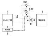
本実施形態の電力変換装置は、図1に示すように、トランスT1を挟んでスイッチング回路1と整流回路2とを備える。スイッチング回路1は、後述するスイッチング素子を備え、スイッチング素子を制御するためにスイッチング回路1には制御部3が付設される。トランスT1の第1巻線n1は、キャパシタC1とインダクタL1との直列回路を介してスイッチング回路1と接続される。整流回路2は、トランスT1の第2巻線n2に接続される。さらに、キャパシタC1にはスイッチSW1が並列に接続される。制御部3は、スイッチSW1のオンオフも制御する。
As shown in FIG. 1, the power converter according to the present embodiment includes a
スイッチング回路1および整流回路2は、たとえば、図2に示す構成を備える。図2に示す構成は、スイッチング回路1および整流回路2の構成を限定する趣旨ではなく一例として示している。また、スイッチング回路1は入力電源として直流電源が接続される。この直流電源は、蓄電池、燃料電池、太陽電池などのほか、商用交流電源を整流した直流電源であってもよい。また、整流回路2から出力される直流電力は、負荷に供給するほか、蓄電池の充電に用いてもよい。
For example, the
図示例のスイッチング回路1は、4個のスイッチング素子Q11〜Q14からなるブリッジ回路を備える。スイッチング素子Q11,Q12の直列回路と、スイッチング素子Q13,Q14の直列回路とは平滑用のキャパシタC11と並列に接続される。
The illustrated
また、図示例の整流回路2は、スイッチング回路1と同構成の回路を用いている。すなわち、整流回路2は、スイッチング素子Q21〜Q24からなるブリッジ回路を備える。スイッチング素子Q21,Q22の直列回路と、スイッチング素子Q23,Q24の直列回路とは平滑用のキャパシタC21と並列に接続される。この整流回路2は、スイッチング素子Q21〜Q24のオンオフを制御すれば、トランスT1を介して双方向に電力の伝達が可能になるが、本実施形態では、双方向に電力変換を行う動作については説明を省略する。
In the illustrated
スイッチング素子Q11〜Q14,Q21〜Q24は、MOSFETを想定している。ただし、スイッチング素子Q11〜Q14,Q21〜Q24として、バイポーラトランジスタのエミッタ−コレクタ間にダイオードを逆並列に接続した構成、あるいはIGBTなどを用いてもよい。これらのスイッチング素子Q11〜Q14,Q21〜Q24は、オン時に一方向あるいは双方向に通電可能であり、オフ時には他方向に通電可能になる。たとえば、スイッチング素子Q11〜Q14,Q21〜Q24がMOSFETである場合、オフ時には、ボディダイオード(寄生ダイオード)を通る経路で通電可能である。 Switching elements Q11 to Q14 and Q21 to Q24 are assumed to be MOSFETs. However, as the switching elements Q11 to Q14 and Q21 to Q24, a configuration in which a diode is connected in antiparallel between the emitter and the collector of the bipolar transistor, or an IGBT may be used. These switching elements Q11 to Q14 and Q21 to Q24 can be energized in one direction or both directions when turned on, and can be energized in the other direction when turned off. For example, when switching elements Q11 to Q14 and Q21 to Q24 are MOSFETs, they can be energized through a path passing through a body diode (parasitic diode) when they are off.
図示例の整流回路2は、スイッチング素子Q21〜Q24のオフ時の機能を利用して全波整流を行う。ただし、スイッチング素子Q21〜Q24のオンオフを制御すれば、同期整流を行うことも可能である。
The
制御部3は、プログラムに従って動作するプロセッサ(マイコン、DSP(Digital Signal Processor)、FPGA(Field-Programmable Gate Array)などから選択される)を備える。制御部3は、整流回路2の出力電流を適宜箇所に設けた電流検出器(図示せず)の出力により監視する機能を有し、電流検出器から出力されるアナログ情報をプロセッサで扱うためにデジタル情報に変換するAD変換器を備える。スイッチング素子Q11〜Q14は、制御部3から与えられるパルス信号によりオンオフが制御され、パルス信号は、周波数と位相とが調節可能になっている。すなわち、制御部3は、パルス信号を生成するパルス生成器を備え、プロセッサからパルス生成器に指示を与えることにより、スイッチング回路1のPFM(Pulse Frequency Moduration)制御とPPM(Pulse Phase shift Moduration)制御とを選択して行う。さらに、制御部3は、プロセッサを動作させるプログラム、プロセッサの動作条件を定めるデータ、プロセッサの動作中に発生するデータなどを格納するためのメモリを備える。
The
スイッチング素子Q11〜Q14をオンオフさせる周波数は、数十Hz〜数百kHzの範囲で適宜に選択される。ここに、スイッチSW1は、スイッチング素子Q11〜Q14のオンオフのタイミングに基づいて制御されるから、指示から数μs〜数十ms程度の時間内で応答することが要求される。そのため、スイッチSW1は、機械式接点を備える電磁継電器を用いるよりも、応答時間の短い半導体スイッチを用いるほうが望ましい。 The frequency at which the switching elements Q11 to Q14 are turned on / off is appropriately selected within the range of several tens of Hz to several hundreds of kHz. Here, since the switch SW1 is controlled based on the on / off timing of the switching elements Q11 to Q14, it is required to respond within a time of about several μs to several tens of ms from the instruction. Therefore, it is preferable to use a semiconductor switch with a short response time as the switch SW1, rather than using an electromagnetic relay having a mechanical contact.
ところで、スイッチSW1がオフであるときには、キャパシタC1はインダクタL1とトランスT1の第1巻線n1との間に接続され、キャパシタC1はインダクタL1とトランスT1とにより共振回路が形成される。したがって、この共振回路の共振周波数に対して、スイッチング回路1の周波数を適宜に調節すれば、この回路は、トランスT1の第2巻線n2に出力される電圧が変化する第1の変換回路として動作する。このように1個のキャパシタC1に対してインダクタL1とともにトランスT1を用いて構成した共振回路を用いて、スイッチング回路1の動作周波数を調節することにより整流回路2の出力電圧を変化させる構成を、以下では「LLC共振型変換回路」と呼ぶ。
By the way, when the switch SW1 is off, the capacitor C1 is connected between the inductor L1 and the first winding n1 of the transformer T1, and the capacitor C1 forms a resonance circuit by the inductor L1 and the transformer T1. Therefore, if the frequency of the
以下では、図2に示す構成において、トランスT1の第1巻線n1を挟んで直列に接続された位置関係の2個のスイッチング素子Q11,Q14およびQ12,Q13を「相対するスイッチング素子」と呼ぶ。LLC共振型変換回路として動作するときには、相対するスイッチング素子Q11,Q14のオンオフが同時に行われ、相対するスイッチング素子Q12,Q13のオンオフが同時に行われる。また、直列接続されたスイッチング素子Q11,Q12は同時にオンにならず、直列接続されたスイッチング素子Q13,Q14が同時にオンになることもない。 In the following, in the configuration shown in FIG. 2, the two switching elements Q11, Q14 and Q12, Q13 that are connected in series with the first winding n1 of the transformer T1 interposed therebetween are referred to as “opposing switching elements”. . When operating as an LLC resonance type conversion circuit, the opposing switching elements Q11 and Q14 are simultaneously turned on and off, and the opposing switching elements Q12 and Q13 are simultaneously turned on and off. Further, the switching elements Q11 and Q12 connected in series are not simultaneously turned on, and the switching elements Q13 and Q14 connected in series are not simultaneously turned on.
図3は、LLC共振型変換回路におけるスイッチング回路1の動作周波数と、整流回路2の出力電圧の電圧ゲインとの関係を示している。また、図3に(1)〜(6)の符号を付している曲線は、負荷の大きさの違いを表している。負荷の大きさは(1)〜(6)の順に大きくなっている。
FIG. 3 shows the relationship between the operating frequency of the
図示例では、軽負荷時に、動作周波数比が0.4付近で電圧ゲインがピークになり、動作周波数比が0.4付近から離れるほど電圧ゲインが減少している。動作周波数比は、キャパシタC1とインダクタL1とにより決まる共振周波数に対するスイッチング回路1の動作周波数の比である。LLC共振型変換回路は、軽負荷であるほど強い共振が生じるから、軽負荷時には共振点付近でスイッチング回路1の動作周波数がわずかに変化するだけでも出力電圧が大きく変動し、出力電圧が不安定になる可能性がある。さらに、軽負荷時には、整流回路2の出力にノイズ成分が多く含まれることになる。
In the illustrated example, when the load is light, the voltage gain peaks when the operating frequency ratio is around 0.4, and the voltage gain decreases as the operating frequency ratio goes away from around 0.4. The operating frequency ratio is the ratio of the operating frequency of the
一方、図3に示す例では、負荷が大きくなると、スイッチング回路1の動作周波数に対する出力電圧の変化は少なくなっているが、電圧ゲインの調節範囲も小さくなっている。すなわち、LLC共振型変換回路において、負荷が大きい領域では共振が弱くなり、スイッチング回路1の動作周波数の変化に対する出力電圧の変動は小さくなる。このとき、整流回路2の出力に含まれるノイズ成分も軽負荷時より減少する。
On the other hand, in the example shown in FIG. 3, when the load increases, the change in the output voltage with respect to the operating frequency of the
以上のように、LLC共振型変換回路は、負荷の大きさによるが、動作周波数比を変化させることにより、入力電圧に対する出力電圧の電圧比(電圧ゲイン)を変化させることができ、しかも昇圧が可能であって、昇圧比の調節が可能になっている。ただし、軽負荷時には動作が不安定になるから、安定に動作する負荷範囲では電圧ゲインの調節範囲は比較的狭くなる。 As described above, the LLC resonant converter circuit can change the voltage ratio (voltage gain) of the output voltage to the input voltage by changing the operating frequency ratio, and the boosting can be increased. The step-up ratio can be adjusted. However, since the operation becomes unstable at a light load, the adjustment range of the voltage gain is relatively narrow in the load range where the operation is stable.
一方、スイッチSW1がオンであるときには、キャパシタC1が短絡されるから、インダクタL1とトランスT1とだけが、スイッチング回路1と整流回路2との間に介在することになる。この場合、インダクタL1とトランスT1の第1巻線n1とに流れる電流の変化により、整流回路2の出力電圧が変化する。この動作では、トランスT1の第1巻線n1に通電することによりトランスT1に蓄積された電磁エネルギーが第2巻線n2に引き渡される。したがって、単位時間当たりにトランスT1に蓄積する電磁エネルギーを調節することにより、この回路は、整流回路2の出力電圧を調節する第2の変換回路として動作する。
On the other hand, since the capacitor C1 is short-circuited when the switch SW1 is on, only the inductor L1 and the transformer T1 are interposed between the switching
トランスT1の第1巻線n1に通電する期間を調節するには、たとえば、図4に示すように、スイッチング素子Q11〜Q14をオンにする位相を制御する。このように、トランスT1の第1巻線n1に単位時間当たりに流す電流を調節するために、スイッチング回路1のスイッチング素子Q11〜Q14をオンにする位相を変化させる構成(つまり、第2の変換回路)を、以下では「フェーズシフト型変換回路」と呼ぶ。
In order to adjust the period during which the first winding n1 of the transformer T1 is energized, for example, as shown in FIG. 4, the phase at which the switching elements Q11 to Q14 are turned on is controlled. In this way, in order to adjust the current that flows in the first winding n1 of the transformer T1 per unit time, the configuration for changing the phase at which the switching elements Q11 to Q14 of the
フェーズシフト型変換回路は、スイッチング回路1を構成している4個のスイッチング素子Q11〜Q14のオンデューティは変化させず、同時にオンにする2個ずつのスイッチング素子Q11〜Q14の位相を変化させる。つまり、出力電力の調節は、相対するスイッチング素子Q11,Q14およびQ12,Q13について同時にオンにする位相を調節することにより行われる。
The phase shift type conversion circuit does not change the on-duty of the four switching elements Q11 to Q14 constituting the
図2に示す回路では、相対するスイッチング素子Q11,Q14が同時にオンである期間と、相対するスイッチングQ12,Q13が同時にオンである期間とに、トランスT1の第1巻線n1に電流が流れる。したがって、相対するスイッチング素子Q11,Q14をオンにする位相を調節するか、相対するスイッチング素子Q12,Q13をオンにする位相を調節すれば、第1巻線n1に通電する時間を調節することになり、結果的に整流回路2の出力電圧が調節される。なお、直列に接続されたスイッチング素子Q11,Q12またはQ13,Q14は同時にオンにすることが禁止され、互いに逆相となるようにオンオフが制御される。つまり、スイッチング素子Q11とスイッチング素子Q12とはオンオフが逆になり、スイッチング素子Q13とスイッチング素子Q14とはオンオフが逆になる。
In the circuit shown in FIG. 2, current flows through the first winding n1 of the transformer T1 during a period in which the opposing switching elements Q11 and Q14 are simultaneously on and a period in which the opposing switching elements Q12 and Q13 are simultaneously on. Therefore, if the phase for turning on the opposing switching elements Q11 and Q14 is adjusted or the phase for turning on the opposing switching elements Q12 and Q13 is adjusted, the time for energizing the first winding n1 is adjusted. As a result, the output voltage of the
図4に示す動作を参照すると、図4(a)〜(d)に示すように、スイッチング素子Q11〜Q14は、いずれもオンデューティが50%に設定され、スイッチング素子Q11とスイッチング素子Q13とのオン期間は位相差Tsだけ異なっている。したがって、相対するスイッチングQ12,Q14およびQ12,Q13のオン期間は位相差Tsに相当する期間だけ重なる。この位相差Tsは、スイッチング素子Q11とスイッチング素子Q13とのオン期間が重ならないときを0度とし、スイッチング素子Q11とスイッチング素子Q13とのオン期間が一致するときを180度とする。つまり、位相差Tsはスイッチング素子Q11〜Q14のオン期間を180度として、相対するスイッチング素子Q11,Q14およびQ12,Q13が同時にオンになる期間を角度で表した値に相当する。 Referring to the operation shown in FIG. 4, as shown in FIGS. 4A to 4D, the switching elements Q11 to Q14 are all set to 50% on-duty, and the switching elements Q11 and Q13 are connected to each other. The on period differs by the phase difference Ts. Therefore, the ON periods of the opposing switching Q12, Q14 and Q12, Q13 overlap for a period corresponding to the phase difference Ts. The phase difference Ts is set to 0 degree when the ON periods of the switching elements Q11 and Q13 do not overlap, and is set to 180 degrees when the ON periods of the switching elements Q11 and Q13 coincide. In other words, the phase difference Ts corresponds to a value in which the on period of the switching elements Q11 to Q14 is 180 degrees and the period in which the opposing switching elements Q11, Q14 and Q12, Q13 are simultaneously turned on is represented by an angle.
スイッチング回路1が上述した動作を行うと、図4(e)に示すように、スイッチング素子Q11〜Q14のオン期間のうち、位相差Tsに相当する期間にのみトランスT1の第1巻線n1に通電される。また、相対するスイッチング素子Q11,Q14が同時にオンである期間と、相対するスイッチング素子Q12,Q13が同時にオンである期間とでは、トランスT1の第1巻線n1に流れる電流の向きが逆転する。この動作により、トランスT1の第2巻線n2には交番電圧が誘起される。
When the
図5は、フェーズシフト型変換回路における位相差Tsと、整流回路2の出力電圧の電圧ゲインとの関係を示している。図5からわかるように、フェーズシフト型変換回路は、電圧ゲインが位相差Tsとほぼ線形の関係を有している。つまり、フェーズシフト型変換回路は、相対するスイッチング素子Q11,Q14およびQ12,Q13のオン期間に関する位相差Tsを調節することにより、整流回路2からの出力電圧を変化させることが可能である。
FIG. 5 shows the relationship between the phase difference Ts in the phase shift type conversion circuit and the voltage gain of the output voltage of the
また、フェーズシフト型変換回路は、入力電圧と出力電圧との電圧比(電圧ゲイン)の調節範囲が比較的広いことも特徴である。図2に示す構成でフェーズシフト型変換回路として動作させる場合、電流休止期間がほとんど生じないから、フォワード型コンバータやフライバック型コンバータと比較するとノイズは少なくなる。ただし、トランスT1の巻線比で決まる電圧を上限値として、上限値以下の電圧範囲でしか電圧の調節はできない。 The phase shift type conversion circuit is also characterized in that the adjustment range of the voltage ratio (voltage gain) between the input voltage and the output voltage is relatively wide. In the case of operating as a phase shift type conversion circuit with the configuration shown in FIG. 2, since there is almost no current pause period, noise is reduced as compared with a forward type converter or a flyback type converter. However, the voltage can be adjusted only in the voltage range below the upper limit value, with the voltage determined by the winding ratio of the transformer T1 as the upper limit value.
上述したように、スイッチSW1のオンオフを切り替え、スイッチング回路1の動作を変更するだけで、LLC共振型変換回路とフェーズシフト型変換回路との両方の動作が可能になっている。したがって、LLC共振型変換回路とフェーズシフト型変換回路との両方の特性を負荷の状態に応じて補完して用いることが可能になる。
As described above, both the LLC resonance type conversion circuit and the phase shift type conversion circuit can be operated simply by switching the switch SW1 on and off and changing the operation of the
また、本実施形態の構成は、LLC共振型変換回路にスイッチSW1を付加し、かつ、フェーズシフト型変換回路としての動作を可能にするプログラムを制御部3に付加すればよい。したがって、LLC共振型変換回路がすでに設計されている場合には、大幅な設計変更を要することなく、LLC共振型変換回路とフェーズシフト型変換回路との両方の機能を持たせた電力変換装置を提供することが可能になる。
In the configuration of the present embodiment, the switch SW1 is added to the LLC resonance type conversion circuit, and a program that enables operation as a phase shift type conversion circuit may be added to the
たとえば、入力電圧が400Vであって、出力電圧を100〜500Vの範囲で変化させようとする場合を想定する。この場合、出力電圧が100〜400Vの範囲では、スイッチSW1をオンにしフェーズシフト型変換回路として動作させることにより、広範囲に出力電圧を調節することが可能である。一方、出力電圧が400〜500Vの範囲では、スイッチSW1をオフにしLLC共振型変換回路として動作させることにより、入力電圧よりも高い電圧範囲の出力電圧が得られることになる。 For example, it is assumed that the input voltage is 400V and the output voltage is to be changed in the range of 100 to 500V. In this case, when the output voltage is in the range of 100 to 400 V, it is possible to adjust the output voltage over a wide range by turning on the switch SW1 and operating as a phase shift type conversion circuit. On the other hand, when the output voltage is in the range of 400 to 500 V, the switch SW1 is turned off to operate as an LLC resonance type conversion circuit, whereby an output voltage in a voltage range higher than the input voltage can be obtained.
また、上述したように電流検出器を設けている場合、出力電流に応じてスイッチSW1のオンオフを定めてもよい。出力電流が規定値(たとえば、1A)以下であって軽負荷である場合はフェーズシフト型変換回路として動作させ、出力電流が規定値を超える場合はLLC共振型変換回路として動作させるようにしてもよい。この動作では、LLC共振型変換回路が不安定な動作になり整流回路2の出力にノイズ成分が増加するような軽負荷の領域では、フェーズシフト型変換回路として動作させることにより、安定かつノイズ成分の少ない動作が可能になる。
Further, when the current detector is provided as described above, the on / off state of the switch SW1 may be determined according to the output current. When the output current is a specified value (for example, 1 A) or less and the load is light, the phase shift converter circuit is operated. When the output current exceeds the specified value, the circuit is operated as an LLC resonant converter circuit. Good. In this operation, in the light load region where the LLC resonance type conversion circuit becomes unstable and the noise component increases in the output of the
スイッチSW1のオンオフを切り替える条件としては、電力の変換効率を考慮する場合もある。たとえば、入力電圧と出力電圧とを所望の電圧比とするために、LLC共振型変換回路とフェーズシフト型変換回路とのどちらを用いてもよい場合には、変換効率に基づいてスイッチSW1のオンオフを定めることが可能である。たとえば、入力電圧と出力電圧とが所望の値である場合に、LLC共振型変換回路の変換効率がE1であり、フェーズシフト型変換回路の変換効率がE2であって、E1>E2であるとすれば、LLC共振型変換回路を用いるほうが変換効率が高いから望ましい。 As a condition for switching on / off of the switch SW1, there is a case where power conversion efficiency is taken into consideration. For example, when either the LLC resonance type conversion circuit or the phase shift type conversion circuit may be used to obtain a desired voltage ratio between the input voltage and the output voltage, the switch SW1 is turned on / off based on the conversion efficiency. Can be determined. For example, when the input voltage and the output voltage are desired values, the conversion efficiency of the LLC resonance type conversion circuit is E1, the conversion efficiency of the phase shift type conversion circuit is E2, and E1> E2. In this case, it is preferable to use the LLC resonance type conversion circuit because the conversion efficiency is high.
なお、上述のように変換効率を考慮してスイッチSW1のオンオフを定める場合は、入力電圧と出力電圧と効率との関係を制御部3に記憶させておく必要がある。また、入力電圧および出力電圧を制御部3に通知する機能も必要である。
Note that, when the on / off state of the switch SW1 is determined in consideration of the conversion efficiency as described above, the relationship between the input voltage, the output voltage, and the efficiency needs to be stored in the
以上のように、スイッチSW1のオンオフを選択し、スイッチング回路1の動作を変更するだけで、LLC共振型変換回路とフェーズシフト型変換回路との動作を切り替えることができる。したがって、出力電圧範囲、負荷の大きさ、変換効率などに着目して、スイッチSW1のオンオフを切り替えることにより、利便性を向上させることになる。
As described above, the operation of the LLC resonance type conversion circuit and the phase shift type conversion circuit can be switched only by selecting ON / OFF of the switch SW1 and changing the operation of the
ところで、LLC共振型変換回路としての動作からフェーズシフト型変換回路としての動作に切り替えるためにスイッチSW1をオフからオンに切り替える際に、キャパシタC1に電荷が蓄積されていることがある。キャパシタC1に電荷が蓄積された状態で、スイッチSW1をオンにすると、スイッチSW1に突入電流が流れる可能性がある。このような突入電流の発生は、スイッチSW1に大きなストレスを与える。また、LLC共振型変換回路の動作とフェーズシフト型変換回路の動作とでは、電圧ゲインが異なるから、スイッチSW1のオンオフを切り替える際に電圧ゲインを考慮しないと、スイッチSW1の切替により出力電圧が変動することになる。 By the way, when the switch SW1 is switched from OFF to ON in order to switch from the operation as the LLC resonance type conversion circuit to the operation as the phase shift type conversion circuit, charge may be accumulated in the capacitor C1. If the switch SW1 is turned on while the electric charge is accumulated in the capacitor C1, an inrush current may flow through the switch SW1. The occurrence of such an inrush current gives a large stress to the switch SW1. Further, since the voltage gain is different between the operation of the LLC resonance type conversion circuit and the operation of the phase shift type conversion circuit, the output voltage fluctuates due to the switching of the switch SW1 unless the voltage gain is taken into consideration when switching the switch SW1 on and off. Will do.
突入電流を防止するには、制御部3は、LLC共振型変換回路として動作させている期間において、インダクタL1とキャパシタC1とトランスT1とからなる共振回路に流れる電流のゼロクロス点に同期させてスイッチSW1をオンにすればよい。共振回路に流れる電流Iqは、図6(a)のような波形になる。この電流Iqの波形は、図6(b)に示すスイッチング素子Q11〜Q14のオンオフのタイミングに同期し、スイッチング素子Q11〜Q14のオンまたはオフのタイミングにおいて、電流Iqの極性が反転してゼロクロス点を通ることになる。
In order to prevent the inrush current, the
このことから、スイッチング素子Q11〜Q14のオンオフを切り替えるタイミングでスイッチSW1をオンにすれば、キャパシタC1の電荷による突入電流がスイッチSW1に流れることが防止される。図示例では、スイッチSW1をオンにするタイミングを矢印の位置で示してあり、このタイミングをスイッチング素子Q11〜Q14がオンになるタイミングに同期させている。図に示すタイミングはスイッチングQ11〜Q14がオンになるタイミングに同期させているが、スイッチング素子Q11〜Q14がオフになるタイミングであってもよい。 Therefore, if the switch SW1 is turned on at the timing of switching on and off the switching elements Q11 to Q14, the inrush current due to the charge of the capacitor C1 is prevented from flowing to the switch SW1. In the illustrated example, the timing at which the switch SW1 is turned on is indicated by the position of the arrow, and this timing is synchronized with the timing at which the switching elements Q11 to Q14 are turned on. The timing shown in the figure is synchronized with the timing when the switching elements Q11 to Q14 are turned on, but may be the timing when the switching elements Q11 to Q14 are turned off.
また、上述の動作はスイッチング素子Q11〜Q14のオンオフのタイミングに同期させているから、制御部3は、スイッチSW1をオンにするタイミングを容易に定めることができる。なお、キャパシタC1の両端電圧を検出するか、共振回路に流れる共振電流を検出し、検出した状態に応じてスイッチSW1をオンにするタイミングを定めることも可能である。
Further, since the above-described operation is synchronized with the on / off timing of the switching elements Q11 to Q14, the
上述の動作によって、LLC共振型変換回路からフェーズシフト型変換回路に移行する際に、キャパシタC1に電荷が蓄積されていない状態でスイッチSW1がオンになる。そのため、スイッチSW1をオンにしたときに、キャパシタC1からスイッチSW1に突入電流が流れることが回避される。つまり、LLC共振型変換回路からフェーズシフト型変換回路への移行をシームレスに行うことができる。 With the above-described operation, the switch SW1 is turned on when no charge is accumulated in the capacitor C1 when the phase shift type conversion circuit is shifted from the LLC resonance type conversion circuit. Therefore, when the switch SW1 is turned on, the inrush current is prevented from flowing from the capacitor C1 to the switch SW1. That is, the transition from the LLC resonance type conversion circuit to the phase shift type conversion circuit can be performed seamlessly.
ところで、LLC共振型変換回路として動作する期間と、フェーズシフト型変換回路として動作する期間とでは、上述したように、スイッチング素子Q11〜Q14のオンオフのタイミングが異なっている。したがって、制御部3は、スイッチSW1のオンオフの際にスイッチング素子Q11〜Q14のオンオフのタイミングも変更する必要がある。しかしながら、LLC共振型変換回路とフェーズシフト型変換回路とでは、スイッチング素子Q11〜Q14のオンオフの位相を瞬時に合わせることは難しい。したがって、スイッチSW1のオンオフを行うタイミングの前後において、スイッチング素子Q11〜Q14のオンオフのタイミングを変更する移行期間を設けることが望ましい。移行期間には、スイッチング素子Q11〜Q14のオンオフを一旦停止させるか、スイッチング素子Q11〜Q14のオンオフのタイミングを強制的に変更することになる。
By the way, as described above, the on / off timings of the switching elements Q11 to Q14 are different between the period of operation as the LLC resonance type conversion circuit and the period of operation as the phase shift type conversion circuit. Therefore, the
LLC共振型変換回路としての動作からフェーズシフト型変換回路としての動作に移行する場合について、スイッチング素子Q11〜Q14のオンオフのタイミングの例を図7に示す。LLC共振変換回路としての動作時には、相対するスイッチング素子Q11,Q14およびQ12,Q13のオンオフのタイミングは一致している。また、フェーズシフト型変換回路としての動作時には、相対するスイッチング素子Q11,Q14およびQ12,Q13のオンのタイミングには適宜の位相差が付与される。 FIG. 7 shows an example of on / off timings of the switching elements Q11 to Q14 in the case of shifting from the operation as the LLC resonance type conversion circuit to the operation as the phase shift type conversion circuit. At the time of operation as the LLC resonance conversion circuit, the on / off timings of the opposing switching elements Q11, Q14 and Q12, Q13 are the same. In the operation as the phase shift type conversion circuit, an appropriate phase difference is given to the on timing of the opposing switching elements Q11, Q14 and Q12, Q13.
そして、LLC共振変換回路としての動作からフェーズシフト型変換回路としての動作への変化時には、すべてのスイッチング素子Q11〜Q14をオフにする移行期間Psが設けられる。制御部3は、この移行期間PsにおいてスイッチSW1をオンにする。
When the operation as the LLC resonance conversion circuit is changed to the operation as the phase shift type conversion circuit, a transition period Ps in which all the switching elements Q11 to Q14 are turned off is provided. The
ところで、LLC共振型変換回路とフェーズシフト型変換回路との間の移行の際に、整流回路2の出力電圧が変動することは好ましくない。したがって、動作移行の際には、制御部3において整流回路2の出力電圧が等しくなるように、スイッチング素子Q11〜Q14のオンオフのタイミングを調節することが必要である。この動作を実現するために、LLC共振型変換回路における動作周波数と電圧ゲインとの関係と、フェーズシフト型変換回路における位相差Tsと電圧ゲインとの関係とが、制御部3に設けた記憶部に格納されている。また、制御部3は、入力電圧および出力電圧と、出力電流とを監視し、LLC共振型変換回路とフェーズシフト型変換回路と移行直前の電圧ゲインに応じて、記憶部を参照することによりスイッチング素子Q11〜Q14のオンオフのタイミングを決定する。この動作により、LLC共振型変換回路とフェーズシフト型変換回路との動作を切り替える際に整流回路2の出力電圧の変動が抑制される。
Incidentally, it is not preferable that the output voltage of the
制御部3に設けた記憶部には、LLC共振型変換回路およびフェーズシフト型変換回路の電圧ゲインと変換効率との関係を記憶させてもよい。すなわち、入力電圧と出力電圧との電圧比(電圧ゲイン)と変換効率との関係が分かっていれば、入力電圧と出力電圧との関係に応じて、変換効率がよいほうの動作を選択することが可能になる。つまり、上述したように、入力電圧と出力電圧とを所望の電圧比とするために、LLC共振型変換回路とフェーズシフト型変換回路とのどちらを用いてもよい場合は、変換効率に基づいてスイッチSW1のオンオフを定めるのである。
The storage unit provided in the
上述した実施形態は、インダクタL1とトランスT1との間にキャパシタC1を挿入しているが、キャパシタC1とトランスT1との間にインダクタL1を挿入する構成でも同様の動作になる。 In the above-described embodiment, the capacitor C1 is inserted between the inductor L1 and the transformer T1, but the same operation is performed even in a configuration in which the inductor L1 is inserted between the capacitor C1 and the transformer T1.
なお、本実施形態は、スイッチング回路1からトランスT1に電力が供給される構成のみを説明しているが、整流回路2に設けられたスイッチング素子Q21〜Q24のオンオフを制御すれば、整流回路2からトランスT1に電力を供給することも可能である。つまり、電力を双方向に伝達することが可能である。また、スイッチング回路1は、図2に示す構成に限定されず、トランスT1の第1巻線n1とキャパシタC1との直列回路に電流を流す期間をスイッチングにより制御する構成であればよい。
In this embodiment, only the configuration in which power is supplied from the switching
(実施形態2)
本実施形態は、図8に示すように、実施形態1の構成におけるスイッチSW1に、スイッチSW2と抵抗R2との直列回路を並列に接続した構成を備える。
(Embodiment 2)
As shown in FIG. 8, the present embodiment has a configuration in which a series circuit of a switch SW2 and a resistor R2 is connected in parallel to the switch SW1 in the configuration of the first embodiment.
本実施形態の構成においてLLC共振型変換回路からフェーズシフト型変換回路に移行させるには、制御部3は、スイッチSW1のオンに先立って、スイッチSW2をオンにする。スイッチSW2をオンにするタイミングは、スイッチング素子Q11〜Q14のオンオフのタイミングに合わせる必要はない。スイッチSW2がオンになると、キャパシタC1に蓄積されている電荷は抵抗R2を介して放電され、スイッチSW2に流れる電流は抵抗R2の抵抗値によって制限される。
In order to shift from the LLC resonance type conversion circuit to the phase shift type conversion circuit in the configuration of the present embodiment, the
さらに、スイッチSW2がオンになりキャパシタC1の電荷量が減少した後、制御部3は、スイッチSW1をオンにする。スイッチSW2がオンになった後のキャパシタC1の電荷量の時間経過は、キャパシタC1の容量および両端電圧と抵抗R2の抵抗値とにより決まる。したがって、スイッチSW2がオンにした後にスイッチSW1をオンにするまでの時間は、キャパシタC1の両端電圧に依存するが、制御を簡便に行う場合は、キャパシタC1の容量と抵抗R2の抵抗値とを用いて一定時間に定めればよい。
Further, after the switch SW2 is turned on and the charge amount of the capacitor C1 is reduced, the
この構成では、スイッチSW1をオンにするタイミングは、共振回路に流れる電流波形に依存しないから、スイッチSW1の応答時間はとくに考慮しなくてもよく、半導体スイッチよりも応答時間の長い電磁継電器を用いることが可能である。本実施形態の他の構成および動作は実施形態1と同様である。 In this configuration, the timing at which the switch SW1 is turned on does not depend on the waveform of the current flowing through the resonance circuit. Therefore, the response time of the switch SW1 does not have to be taken into consideration, and an electromagnetic relay having a response time longer than that of the semiconductor switch is used. It is possible. Other configurations and operations in the present embodiment are the same as those in the first embodiment.
(実施形態3)
本実施形態は、実施形態1の変形例であって、図9に示すように、図1に示したインダクタL1に代えて、複数個(図示例は3個)ずつのインダクタL31〜L33とスイッチSW31〜SW33とを用いている。スイッチSW31〜SW33は、それぞれインダクタL31〜L33の個々に並列に接続されている。したがって、スイッチSW31〜SW33のオンオフの組合せによって、インダクタL31〜L33のいずれかが共振回路に用いられる。言い換えると、スイッチSW31〜SW33のオンオフの組合せにより共振回路に用いるインダクタンスが調節され、結果的に複数の共振周波数を選択することが可能になる。
(Embodiment 3)
The present embodiment is a modification of the first embodiment. As shown in FIG. 9, instead of the inductor L1 shown in FIG. 1, a plurality (three in the illustrated example) of inductors L31 to L33 and switches are provided. SW31 to SW33 are used. The switches SW31 to SW33 are individually connected in parallel to the inductors L31 to L33, respectively. Therefore, any one of the inductors L31 to L33 is used in the resonance circuit depending on the combination of ON and OFF of the switches SW31 to SW33. In other words, the inductance used in the resonance circuit is adjusted by the combination of on / off of the switches SW31 to SW33, and as a result, a plurality of resonance frequencies can be selected.
たとえば、図示する構成であれば、スイッチSW31をオフにし、スイッチSW32,SW33をオンにすれば、インダクタL31のみが共振回路において有効に機能する。また、スイッチSW31〜SW33をすべてオフにすれば、3個のインダクタL31〜L33の直列回路が共振回路において有効に機能する。したがって、共振回路の共振周波数を広範囲に変化させることが可能になる。 For example, in the configuration shown in the figure, when the switch SW31 is turned off and the switches SW32 and SW33 are turned on, only the inductor L31 functions effectively in the resonance circuit. If all the switches SW31 to SW33 are turned off, the series circuit of the three inductors L31 to L33 functions effectively in the resonance circuit. Therefore, the resonance frequency of the resonance circuit can be changed over a wide range.
図9の構成に代えて、図1に示したインダクタL1に代えて、図10に示す接続関係になるように、複数個(図示例は3個)ずつのインダクタL41〜L43とスイッチSW41〜SW43とを用いてもよい。この構成では、3個のインダクタL41〜L43が直列接続され、3個のスイッチSW41〜SW43の一端がインダクタL41〜L43の直列回路の一端に接続される。また、3個のスイッチSW41〜SW43のそれぞれの他端が、インダクタL41〜L43の一端に接続される。つまり、インダクタL41にスイッチSW41が並列接続され、インダクタL41,L42の直列回路にスイッチSW42が並列接続され、インダクタL41〜L43の直列回路にスイッチSW43が並列接続される。 In place of the configuration of FIG. 9, instead of the inductor L1 shown in FIG. 1, a plurality (three in the illustrated example) of inductors L41 to L43 and switches SW41 to SW43 are provided so as to have the connection relationship shown in FIG. And may be used. In this configuration, three inductors L41 to L43 are connected in series, and one end of each of the three switches SW41 to SW43 is connected to one end of a series circuit of the inductors L41 to L43. The other ends of the three switches SW41 to SW43 are connected to one ends of the inductors L41 to L43. That is, the switch SW41 is connected in parallel to the inductor L41, the switch SW42 is connected in parallel to the series circuit of the inductors L41 and L42, and the switch SW43 is connected in parallel to the series circuit of the inductors L41 to L43.
図9に示した構成は、選択可能なインダクタンスの種類が、スイッチSW31〜SW33のオンオフの組合せ数で決まるが、図10に示す構成は、選択可能なインダクタンスの種類が、スイッチSW41〜SW43の個数より1種類だけ多い数になる。つまり、図10に示す構成では、スイッチSW43がオン、スイッチSW43がオフかつスイッチSW42がオン、スイッチSW42,SW43がオフかつスイッチSW41がオン、スイッチSW41〜SW43がオフの4種類の状態のみが選択可能である。ただし、図10に示す構成は、共振回路に含まれるスイッチSW41〜SW43が1個以下であるのに対して、図9に示す構成は共振回路に含まれるスイッチSW31〜SW33が0〜3個の範囲で変化する。そのため、スイッチによる共振回路の平均的な損失は図10に示す構成のほうが図9に示す構成よりも少なくなる。 In the configuration shown in FIG. 9, the type of inductance that can be selected is determined by the number of on / off combinations of the switches SW31 to SW33, but in the configuration shown in FIG. 10, the type of inductance that can be selected is the number of switches SW41 to SW43. Only one more number. In other words, in the configuration shown in FIG. 10, only four types of states are selected: the switch SW43 is on, the switch SW43 is off and the switch SW42 is on, the switches SW42 and SW43 are off and the switch SW41 is on, and the switches SW41 to SW43 are off. Is possible. However, the configuration illustrated in FIG. 10 includes one or less switches SW41 to SW43 included in the resonance circuit, whereas the configuration illustrated in FIG. 9 includes 0 to 3 switches SW31 to SW33 included in the resonance circuit. Varies with range. Therefore, the average loss of the resonance circuit due to the switch is less in the configuration shown in FIG. 10 than in the configuration shown in FIG.
本実施形態は、インダクタおよびスイッチを3個ずつ設けているが、共振周波数を変化させようとする種類に応じて、インダクタおよびスイッチの個数は任意に選択される。他の構成および動作は実施形態1と同様であり、また、実施形態2のようにスイッチSW2および抵抗R2を設けた構成と組み合わせることも可能である。
(実施形態4)
本実施形態は、実施形態1の変形例であって、図11に示すように、図1に示したキャパシタC1に代えて、複数個(図示例は3個)ずつのキャパシタC51〜C53とスイッチSW51〜SW53とを用いている。スイッチSW51〜SW53は、それぞれキャパシタC51〜C53の個々に並列に接続されている。したがって、スイッチSW51〜SW53のオンオフの組合せによって、キャパシタC51〜C53のいずれかが共振回路に用いられる。言い換えると、スイッチSW51〜SW53のオンオフの組合せにより共振回路に用いるキャパシタンスが調節され、結果的に複数の共振周波数を選択することが可能になる。
In the present embodiment, three inductors and switches are provided, but the number of inductors and switches is arbitrarily selected according to the type for which the resonance frequency is to be changed. Other configurations and operations are the same as those in the first embodiment, and can be combined with a configuration in which the switch SW2 and the resistor R2 are provided as in the second embodiment.
(Embodiment 4)
The present embodiment is a modification of the first embodiment. As shown in FIG. 11, instead of the capacitor C1 shown in FIG. 1, a plurality (three in the illustrated example) of capacitors C51 to C53 and switches are provided. SW51 to SW53 are used. The switches SW51 to SW53 are connected in parallel to the capacitors C51 to C53, respectively. Therefore, any one of the capacitors C51 to C53 is used in the resonance circuit depending on the combination of ON / OFF of the switches SW51 to SW53. In other words, the capacitance used for the resonance circuit is adjusted by the combination of on / off of the switches SW51 to SW53, and as a result, a plurality of resonance frequencies can be selected.
また、図示例では、インダクタL1に代えてインダクタL3を用い、インダクタL3にはスイッチSW3を並列接続してある。したがって、スイッチSW3のオンオフにより、共振回路にインダクタL3を含めるか含めないかを選択することが可能になる。 In the illustrated example, an inductor L3 is used instead of the inductor L1, and a switch SW3 is connected in parallel to the inductor L3. Therefore, it is possible to select whether or not to include the inductor L3 in the resonance circuit by turning on and off the switch SW3.
たとえば、図示する構成であれば、スイッチSW51をオフにし、スイッチSW52,SW53をオンにすれば、キャパシタC51のみが共振回路において有効に機能する。また、スイッチSW51〜SW53をすべてオフにすれば、3個のキャパシタC51〜C53の直列回路が共振回路において有効に機能する。したがって、共振回路の共振周波数を広範囲に変化させることが可能になる。 For example, in the illustrated configuration, when the switch SW51 is turned off and the switches SW52 and SW53 are turned on, only the capacitor C51 functions effectively in the resonance circuit. If all the switches SW51 to SW53 are turned off, the series circuit of the three capacitors C51 to C53 functions effectively in the resonance circuit. Therefore, the resonance frequency of the resonance circuit can be changed over a wide range.
図11の構成に代えて、図1に示したキャパシタC1に代えて、図12に示す接続関係になるように、複数個(図示例は3個)ずつのキャパシタC61〜C63とスイッチSW61〜SW63とを用いてもよい。この構成では、3個のキャパシタC61〜C63が直列接続され、3個のスイッチSW61〜SW63の一端がキャパシタC61〜C63の直列回路の一端に接続される。また、3個のスイッチSW61〜SW63のそれぞれの他端が、キャパシタC61〜C63の一端に接続される。つまり、キャパシタC61にスイッチSW61が並列接続され、キャパシタC61,C62の直列回路にスイッチSW62が並列接続され、キャパシタC61〜C63の直列回路にスイッチSW63が並列接続される。 In place of the configuration of FIG. 11, instead of the capacitor C1 shown in FIG. 1, a plurality (three in the illustrated example) of capacitors C61 to C63 and switches SW61 to SW63 are provided so as to have the connection relationship shown in FIG. And may be used. In this configuration, three capacitors C61 to C63 are connected in series, and one end of each of the three switches SW61 to SW63 is connected to one end of a series circuit of the capacitors C61 to C63. The other ends of the three switches SW61 to SW63 are connected to one ends of the capacitors C61 to C63. That is, the switch SW61 is connected in parallel to the capacitor C61, the switch SW62 is connected in parallel to the series circuit of the capacitors C61 and C62, and the switch SW63 is connected in parallel to the series circuit of the capacitors C61 to C63.
図11に示した構成は、選択可能なキャパシタンスの種類が、スイッチSW51〜SW53のオンオフの組合せ数で決まるが、図12に示す構成は、選択可能なキャパシタンスの種類が、スイッチSW61〜SW63の個数より1種類だけ多い数になる。つまり、図12に示す構成では、スイッチSW63がオン、スイッチSW63がオフかつスイッチSW62がオン、スイッチSW62,SW63がオフかつスイッチSW61がオン、スイッチSW61〜SW63がオフの4種類の状態のみが選択可能である。ただし、図12に示す構成は、共振回路に含まれるスイッチSW61〜SW63が1個以下であるのに対して、図11に示す構成は共振回路に含まれるスイッチSW51〜SW53が0〜3個の範囲で変化する。そのため、スイッチによる共振回路の平均的な損失は図12に示す構成のほうが図11に示す構成よりも少なくなる。 In the configuration shown in FIG. 11, the type of capacitance that can be selected is determined by the number of on / off combinations of the switches SW51 to SW53, but in the configuration shown in FIG. 12, the type of capacitance that can be selected is the number of switches SW61 to SW63. Only one more number. In other words, in the configuration shown in FIG. 12, only four types of states are selected: the switch SW63 is on, the switch SW63 is off and the switch SW62 is on, the switches SW62 and SW63 are off and the switch SW61 is on, and the switches SW61 to SW63 are off. Is possible. However, the configuration illustrated in FIG. 12 includes one or less switches SW61 to SW63 included in the resonance circuit, whereas the configuration illustrated in FIG. 11 includes 0 to 3 switches SW51 to SW53 included in the resonance circuit. Varies with range. Therefore, the average loss of the resonance circuit due to the switch is less in the configuration shown in FIG. 12 than in the configuration shown in FIG.
また、実施形態1において説明したように、スイッチSW51〜SW53,SW61〜SW63をオンにするタイミングは、スイッチング回路1に設けたスイッチング素子Q11〜Q14のオンオフのタイミングに同期させて制御される。したがって、キャパシタC51〜C53,C61〜C63の電荷によるスイッチSW51〜SW53,SW61〜SW63への突入電流が防止される。
Further, as described in the first embodiment, the timing of turning on the switches SW51 to SW53 and SW61 to SW63 is controlled in synchronization with the on / off timing of the switching elements Q11 to Q14 provided in the
本実施形態は、キャパシタおよびスイッチを3個ずつ設けているが、共振周波数を変化させようとする種類に応じて、キャパシタおよびスイッチの個数は任意に選択される。他の構成および動作は実施形態1と同様であり、また、実施形態2のようにスイッチSW2および抵抗R2を設けた構成と組み合わせることも可能である。さらに、本実施形態の構成と実施形態3に示した構成とを組み合わせることも可能である。
In this embodiment, three capacitors and three switches are provided, but the number of capacitors and switches is arbitrarily selected according to the type of the resonance frequency to be changed. Other configurations and operations are the same as those in the first embodiment, and can be combined with a configuration in which the switch SW2 and the resistor R2 are provided as in the second embodiment. Furthermore, the configuration of the present embodiment and the configuration shown in
1 スイッチング回路
2 整流回路
3 制御部
C1 キャパシタ
C51〜C53 (第2の)キャパシタ
C61〜C63 (第2の)キャパシタ
L1 インダクタ
L31〜L33 インダクタ
L41〜L43 インダクタ
n1 第1巻線
n2 第2巻線
R2 抵抗
SW1 (第1の)スイッチ
SW2 (第2の)スイッチ
SW31〜SW33 (第3の)スイッチ
SW41〜SW43 (第3の)スイッチ
SW51〜SW53 (第4の)スイッチ
SW61〜SW63 (第4の)スイッチ
T1 トランス
DESCRIPTION OF
Claims (7)
前記トランスの一方の巻線と直列に接続された共振用のキャパシタと、
前記トランスの前記一方の巻線と前記キャパシタとの直列回路に流す電流を入切するスイッチング回路と、
前記トランスの他方の巻線に誘起された電力を整流して出力する整流回路と、
前記キャパシタに並列に接続された第1のスイッチと、
前記トランスの前記一方の巻線と前記キャパシタとの直列回路に電流を流す期間および前記第1のスイッチのオンオフを制御する制御部と、
前記キャパシタに並列接続された第2のスイッチおよび抵抗の直列回路とを備え、
前記制御部は、前記第1のスイッチをオフにし前記スイッチング回路の動作周波数を制御する第1の変換回路を構成する動作と、前記第1のスイッチをオンにし前記スイッチング回路から前記トランスの前記一方の巻線への通電期間を制御する第2の変換回路を構成する動作とを選択し、前記第1の変換回路の動作から前記第2の変換回路の動作に移行させる際に、前記第2のスイッチをオンにした後、前記第1のスイッチをオンにする
ことを特徴とする電力変換装置。 A transformer that transmits power between the input and output;
A resonance capacitor connected in series with one winding of the transformer;
A switching circuit for turning on and off a current flowing in a series circuit of the one winding of the transformer and the capacitor;
A rectifying circuit that rectifies and outputs power induced in the other winding of the transformer;
A first switch connected in parallel to the capacitor;
A control unit for controlling a period for passing a current through a series circuit of the one winding of the transformer and the capacitor and on / off of the first switch ;
A second switch connected in parallel to the capacitor and a series circuit of resistors ;
The control unit turns off the first switch to configure a first conversion circuit that controls the operating frequency of the switching circuit, and turns on the first switch to turn on the one of the transformers from the switching circuit. When the operation of the second conversion circuit that controls the energization period to the winding of the second conversion circuit is selected and the operation of the first conversion circuit is shifted to the operation of the second conversion circuit, the second conversion circuit is selected. After turning on the switch, the first switch is turned on .
ことを特徴とする請求項1記載の電力変換装置。 The control unit switches the operation of the switching circuit between the operation of the first conversion circuit and the operation of the second conversion circuit when switching between the operation of the first conversion circuit and the operation of the second conversion circuit. The power conversion device according to claim 1, further comprising a transition period in which the operation is different from the operation .
前記第1の変換回路の動作と前記第2の変換回路の動作とを切り替える際に、切替後の入力電圧と出力電圧との関係を、切替前の入力電圧と出力電圧との関係と一致させるように、記憶している動作周波数および通電期間に応じて前記スイッチング回路を制御する
ことを特徴とする請求項1又は2記載の電力変換装置。 The control unit includes an operating frequency of the switching circuit in the operation of the first conversion circuit, and an energization period from the switching circuit to the one winding of the transformer in the operation of the second conversion circuit. , Stored in association with the relationship between the input voltage and the output voltage,
When switching between the operation of the first conversion circuit and the operation of the second conversion circuit, the relationship between the input voltage and the output voltage after switching is matched with the relationship between the input voltage and the output voltage before switching. The power converter according to claim 1 or 2, wherein the switching circuit is controlled according to the stored operating frequency and energization period .
入力電圧と出力電圧との関係が、前記第1の変換回路の動作と前記第2の変換回路の動作との両方の動作範囲であるときに、記憶している変換効率が高いほうの動作を選択する
ことを特徴とする請求項1〜3のいずれか1項に記載の電力変換装置。 The control unit stores the conversion efficiency in the operation of the first conversion circuit and the conversion efficiency in the operation of the second conversion circuit in association with the voltage ratio between the input voltage and the output voltage,
When the relationship between the input voltage and the output voltage is the operation range of both the operation of the first conversion circuit and the operation of the second conversion circuit, the operation having the higher stored conversion efficiency is performed. power converter according to claim 1, wherein the selecting.
ことを特徴とする請求項1〜4のいずれか1項に記載の電力変換装置。 5. The power conversion device according to claim 1 , further comprising a resonance inductor connected between the one winding of the transformer and the switching circuit .
前記インダクタのうちの少なくとも1個を短絡する第3のスイッチとをさらに備える
ことを特徴とする請求項1〜4のいずれか1項に記載の電力変換装置。 A plurality of resonant inductors connected between the one winding of the transformer and the switching circuit;
The power converter according to any one of claims 1 to 4 , further comprising a third switch that short-circuits at least one of the inductors .
前記トランスの前記一方の巻線と前記スイッチング回路との間に接続される共振用の複数個の第2のキャパシタと、
前記第2のキャパシタのうちの少なくとも1個を短絡する第4のスイッチとを備える
ことを特徴とする請求項1〜6のいずれか1項に記載の電力変換装置。 The capacitor is
A plurality of second capacitors for resonance connected between the one winding of the transformer and the switching circuit;
The power converter according to claim 1, further comprising a fourth switch that short-circuits at least one of the second capacitors .
Priority Applications (4)
| Application Number | Priority Date | Filing Date | Title |
|---|---|---|---|
| JP2012136174A JP5906418B2 (en) | 2012-06-15 | 2012-06-15 | Power converter |
| PCT/JP2013/003211 WO2013186991A1 (en) | 2012-06-15 | 2013-05-21 | Electric power conversion device |
| US14/407,910 US9160242B2 (en) | 2012-06-15 | 2013-05-21 | Electric power conversion device |
| EP13804652.9A EP2863531A4 (en) | 2012-06-15 | 2013-05-21 | Electric power conversion device |
Applications Claiming Priority (1)
| Application Number | Priority Date | Filing Date | Title |
|---|---|---|---|
| JP2012136174A JP5906418B2 (en) | 2012-06-15 | 2012-06-15 | Power converter |
Publications (2)
| Publication Number | Publication Date |
|---|---|
| JP2014003764A JP2014003764A (en) | 2014-01-09 |
| JP5906418B2 true JP5906418B2 (en) | 2016-04-20 |
Family
ID=49757840
Family Applications (1)
| Application Number | Title | Priority Date | Filing Date |
|---|---|---|---|
| JP2012136174A Active JP5906418B2 (en) | 2012-06-15 | 2012-06-15 | Power converter |
Country Status (4)
| Country | Link |
|---|---|
| US (1) | US9160242B2 (en) |
| EP (1) | EP2863531A4 (en) |
| JP (1) | JP5906418B2 (en) |
| WO (1) | WO2013186991A1 (en) |
Families Citing this family (31)
| Publication number | Priority date | Publication date | Assignee | Title |
|---|---|---|---|---|
| US9112422B1 (en) | 2010-03-09 | 2015-08-18 | Vlt, Inc. | Fault tolerant power converter |
| US9859803B2 (en) * | 2013-04-23 | 2018-01-02 | Analog Devices Global | Transformer-based isolated bi-directional DC-DC power converter, and method and controller for using same |
| EP3095181B1 (en) * | 2014-07-21 | 2020-12-16 | Huawei Technologies Co. Ltd. | Bi-directional dc-dc converter |
| KR101664572B1 (en) * | 2014-11-06 | 2016-10-10 | 엘지이노텍 주식회사 | Power converter |
| KR102291851B1 (en) * | 2014-12-29 | 2021-08-23 | 주식회사 솔루엠 | Apparatus for power supplying |
| WO2016125374A1 (en) * | 2015-02-02 | 2016-08-11 | 三菱電機株式会社 | Dc/dc converter |
| DE102015106335A1 (en) * | 2015-04-24 | 2016-10-27 | Dr. Ing. H.C. F. Porsche Aktiengesellschaft | Method for operating a DC-DC converter |
| JP6141908B2 (en) * | 2015-05-18 | 2017-06-07 | 東芝デベロップメントエンジニアリング株式会社 | Current resonance type DC-DC converter |
| JP2016226134A (en) * | 2015-05-29 | 2016-12-28 | 株式会社日立製作所 | Electric power conversion device and electric power conversion control method |
| US9325247B1 (en) * | 2015-10-02 | 2016-04-26 | Vlt, Inc. | Clamped capacitor resonant power converter |
| CN105406724A (en) * | 2015-12-31 | 2016-03-16 | 西安爱科赛博电气股份有限公司 | Phase-shifting control full-bridge zero-current converter and direct-current switching power source |
| US10785871B1 (en) | 2018-12-12 | 2020-09-22 | Vlt, Inc. | Panel molded electronic assemblies with integral terminals |
| US10277105B1 (en) | 2016-04-05 | 2019-04-30 | Vlt, Inc. | Method and apparatus for delivering power to semiconductors |
| US11336167B1 (en) | 2016-04-05 | 2022-05-17 | Vicor Corporation | Delivering power to semiconductor loads |
| US10158357B1 (en) | 2016-04-05 | 2018-12-18 | Vlt, Inc. | Method and apparatus for delivering power to semiconductors |
| US10903734B1 (en) | 2016-04-05 | 2021-01-26 | Vicor Corporation | Delivering power to semiconductor loads |
| CN106787769A (en) * | 2017-02-24 | 2017-05-31 | 北京新能源汽车股份有限公司 | Bidirectional full-bridge LLC conversion circuit and automobile |
| JP2018174648A (en) | 2017-03-31 | 2018-11-08 | オムロン株式会社 | Llc resonance converter |
| JP2019041531A (en) | 2017-08-28 | 2019-03-14 | オムロン株式会社 | LLC resonant converter |
| EP3462589A1 (en) * | 2017-09-29 | 2019-04-03 | Siemens Aktiengesellschaft | Resonant dc chopper with integrated step up and step down converter |
| CN108237943B (en) * | 2018-01-17 | 2019-05-17 | 深圳威迈斯新能源股份有限公司 | A kind of dual output port charging circuit and its control method |
| WO2019144241A1 (en) * | 2018-01-29 | 2019-08-01 | Queen's University At Kingston | Resonant power converters and control methods for wide input and output voltage ranges |
| WO2019170781A1 (en) * | 2018-03-06 | 2019-09-12 | Npc Tech Aps | A resonant power converter |
| JP7012239B2 (en) | 2018-04-26 | 2022-01-28 | パナソニックIpマネジメント株式会社 | Power converter |
| US10622905B2 (en) * | 2018-07-10 | 2020-04-14 | Sharp Kabushiki Kaisha | DC-DC converter |
| US11329542B2 (en) * | 2019-03-01 | 2022-05-10 | Sharp Kabushiki Kaisha | Switching regulator |
| FR3093875B1 (en) | 2019-03-14 | 2024-08-09 | Safran | ISOLATED AND RECONFIGURABLE POWER CONVERTER |
| TWI688195B (en) | 2019-06-19 | 2020-03-11 | 宏碁股份有限公司 | Power supply device |
| JP7491080B2 (en) * | 2020-06-22 | 2024-05-28 | 富士電機株式会社 | Power Conversion Equipment |
| JPWO2022190162A1 (en) * | 2021-03-08 | 2022-09-15 | ||
| JP7264940B2 (en) | 2021-06-08 | 2023-04-25 | 本田技研工業株式会社 | Converter, converter control device, and converter control method |
Family Cites Families (19)
| Publication number | Priority date | Publication date | Assignee | Title |
|---|---|---|---|---|
| US4951185A (en) | 1989-07-13 | 1990-08-21 | General Electric Company | Resonant inverter employing frequency and phase modulation using optimal trajectory control |
| JP2588786B2 (en) * | 1990-02-26 | 1997-03-12 | オリジン電気株式会社 | X-ray power supply |
| JPH04125062A (en) * | 1990-09-12 | 1992-04-24 | Toyota Autom Loom Works Ltd | Series resonance type dc-dc converter |
| US5438497A (en) * | 1993-05-13 | 1995-08-01 | Northern Telecom Limited | Tertiary side resonant DC/DC converter |
| US7212414B2 (en) * | 1999-06-21 | 2007-05-01 | Access Business Group International, Llc | Adaptive inductive power supply |
| WO2001084699A1 (en) * | 2000-04-28 | 2001-11-08 | Tdk Corporation | Power converting device |
| US6195270B1 (en) * | 2000-06-19 | 2001-02-27 | Technical Witts, Inc. | Self clamping zero voltage switching DC transformers |
| JP4617025B2 (en) * | 2001-05-29 | 2011-01-19 | キヤノン株式会社 | Resonant power supply |
| KR100541724B1 (en) * | 2002-11-08 | 2006-01-11 | 삼성전자주식회사 | power supply apparatus for motor and controlling method thereof |
| JP4400065B2 (en) * | 2003-02-26 | 2010-01-20 | オムロン株式会社 | Switching power supply |
| JP2005065395A (en) * | 2003-08-11 | 2005-03-10 | Sony Corp | Power unit |
| JP4635584B2 (en) * | 2004-11-30 | 2011-02-23 | Tdk株式会社 | Switching power supply |
| US7796406B2 (en) * | 2007-07-31 | 2010-09-14 | Lumenis Ltd. | Apparatus and method for high efficiency isolated power converter |
| US7817452B2 (en) * | 2007-08-13 | 2010-10-19 | Stephen William Smith | Phase shifted H-Bridge resonant converter with symmetrical currents |
| JP5241571B2 (en) * | 2009-03-05 | 2013-07-17 | 富士通テレコムネットワークス株式会社 | Switching power supply |
| JP5632191B2 (en) | 2010-04-28 | 2014-11-26 | パナソニック株式会社 | Bidirectional DC / DC converter |
| GB201013847D0 (en) * | 2010-08-18 | 2010-09-29 | Texas Instr Cork Ltd | Power converter control arrangement |
| CN202218161U (en) * | 2011-08-30 | 2012-05-09 | 刘闯 | Bidirectional isolation-type phase-shift full-bridge DC/DC (Direct Current to Direct Current) converter |
| CN103795251A (en) * | 2012-10-29 | 2014-05-14 | 台达电子工业股份有限公司 | Power converter and control method thereof |
-
2012
- 2012-06-15 JP JP2012136174A patent/JP5906418B2/en active Active
-
2013
- 2013-05-21 WO PCT/JP2013/003211 patent/WO2013186991A1/en active Application Filing
- 2013-05-21 EP EP13804652.9A patent/EP2863531A4/en not_active Withdrawn
- 2013-05-21 US US14/407,910 patent/US9160242B2/en active Active
Also Published As
| Publication number | Publication date |
|---|---|
| EP2863531A4 (en) | 2015-12-02 |
| US9160242B2 (en) | 2015-10-13 |
| WO2013186991A1 (en) | 2013-12-19 |
| JP2014003764A (en) | 2014-01-09 |
| US20150124490A1 (en) | 2015-05-07 |
| EP2863531A1 (en) | 2015-04-22 |
Similar Documents
| Publication | Publication Date | Title |
|---|---|---|
| JP5906418B2 (en) | Power converter | |
| EP3787171A1 (en) | Isolated dc/dc converters for wide output voltage range and control methods thereof | |
| JP6067116B2 (en) | DC / DC converter | |
| JP5762617B2 (en) | DC / DC converter | |
| JP5621193B2 (en) | Power converter | |
| EP2001113A2 (en) | Isolated high power bi-directional DC-DC converter | |
| JP6623585B2 (en) | Switching power supply | |
| JP5089359B2 (en) | Power converter | |
| JP2008099512A (en) | Power supply unit | |
| JP2011120370A (en) | Dc-dc bidirectional converter circuit | |
| JP6526546B2 (en) | Resonant type power supply | |
| JP6065753B2 (en) | DC / DC converter and battery charge / discharge device | |
| JP5857998B2 (en) | DRIVE DEVICE AND VEHICLE HAVING DRIVE DEVICE | |
| JP2007221892A (en) | Power conversion device | |
| JP6727144B2 (en) | Bidirectional isolated DC/DC converter | |
| JP6482009B2 (en) | Multi-input converter and bidirectional converter | |
| JP5678860B2 (en) | AC / DC converter | |
| JP2006081263A (en) | Bidirectional dc-dc converter | |
| JP2013212023A (en) | Bidirectional power conversion device | |
| JP5535290B2 (en) | Bidirectional converter | |
| JPH11113191A (en) | Uninterruptible power-supply apparatus and its charging control method | |
| JP2011160603A (en) | Fuel cell generator | |
| JP2000188867A (en) | Converter circuit and device for controlling dc voltage | |
| JP6270753B2 (en) | Power converter | |
| JP3874291B2 (en) | Power supply |
Legal Events
| Date | Code | Title | Description |
|---|---|---|---|
| A711 | Notification of change in applicant |
Free format text: JAPANESE INTERMEDIATE CODE: A711 Effective date: 20141003 |
|
| A621 | Written request for application examination |
Free format text: JAPANESE INTERMEDIATE CODE: A621 Effective date: 20150219 |
|
| A131 | Notification of reasons for refusal |
Free format text: JAPANESE INTERMEDIATE CODE: A131 Effective date: 20151006 |
|
| A521 | Request for written amendment filed |
Free format text: JAPANESE INTERMEDIATE CODE: A523 Effective date: 20151116 |
|
| TRDD | Decision of grant or rejection written | ||
| A01 | Written decision to grant a patent or to grant a registration (utility model) |
Free format text: JAPANESE INTERMEDIATE CODE: A01 Effective date: 20151208 |
|
| A61 | First payment of annual fees (during grant procedure) |
Free format text: JAPANESE INTERMEDIATE CODE: A61 Effective date: 20160106 |
|
| R151 | Written notification of patent or utility model registration |
Ref document number: 5906418 Country of ref document: JP Free format text: JAPANESE INTERMEDIATE CODE: R151 |