JP5887331B2 - Solder composition - Google Patents
Solder composition Download PDFInfo
- Publication number
- JP5887331B2 JP5887331B2 JP2013271690A JP2013271690A JP5887331B2 JP 5887331 B2 JP5887331 B2 JP 5887331B2 JP 2013271690 A JP2013271690 A JP 2013271690A JP 2013271690 A JP2013271690 A JP 2013271690A JP 5887331 B2 JP5887331 B2 JP 5887331B2
- Authority
- JP
- Japan
- Prior art keywords
- mass
- component
- acid
- solder
- flux
- Prior art date
- Legal status (The legal status is an assumption and is not a legal conclusion. Google has not performed a legal analysis and makes no representation as to the accuracy of the status listed.)
- Active
Links
Images
Classifications
-
- B—PERFORMING OPERATIONS; TRANSPORTING
- B23—MACHINE TOOLS; METAL-WORKING NOT OTHERWISE PROVIDED FOR
- B23K—SOLDERING OR UNSOLDERING; WELDING; CLADDING OR PLATING BY SOLDERING OR WELDING; CUTTING BY APPLYING HEAT LOCALLY, e.g. FLAME CUTTING; WORKING BY LASER BEAM
- B23K35/00—Rods, electrodes, materials, or media, for use in soldering, welding, or cutting
- B23K35/22—Rods, electrodes, materials, or media, for use in soldering, welding, or cutting characterised by the composition or nature of the material
- B23K35/36—Selection of non-metallic compositions, e.g. coatings or fluxes; Selection of soldering or welding materials, conjoint with selection of non-metallic compositions, both selections being of interest
- B23K35/362—Selection of compositions of fluxes
Landscapes
- Engineering & Computer Science (AREA)
- Mechanical Engineering (AREA)
- Electric Connection Of Electric Components To Printed Circuits (AREA)
Description
本発明は、はんだ組成物に関する。 The present invention relates to a solder composition.
回路基板などの筐体用途においては、電子機器の小型化や高密度化にともなって、狭い筐体内部や間隙がほとんど無い状態で部品が装填される。このような場合に、部品の温度上昇を抑制する必要が生じている。そのため、筐体用途においては、放熱性を有する材料が必要とされている。また、電子機器の小型化や高密度化にともなって筐体材料をゲージダウンして軽量化することも求められている。そのため、高強度が要求される用途には厚さが薄くても十分な強度を有し、切断端面に錆を生じることのないステンレス鋼板が用いられている。しかしながら、ステンレス鋼板ははんだぬれ性が不良であり、はんだ付けが必要とされる用途に適用することが困難であった。 In a case of a housing such as a circuit board, components are loaded in a narrow housing or with almost no gap as the electronic equipment is miniaturized and densified. In such a case, it is necessary to suppress the temperature rise of the parts. Therefore, a material having a heat dissipation property is required for use in a casing. In addition, as electronic devices become smaller and higher in density, it is also required to reduce the weight of the casing material by gauge down. For this reason, a stainless steel plate that has sufficient strength even if it is thin and does not cause rust on the cut end face is used for applications that require high strength. However, the stainless steel plate has poor solder wettability, and it has been difficult to apply it to applications that require soldering.
そこで、ステンレス鋼板のはんだぬれ性を改良する技術として、鋼板上にスズメッキを施し、次いでスズメッキ上に亜鉛、ニッケル、コバルトのいずれか1種以上を主成分とするメッキなどを施した、はんだ用二層メッキ鋼板が開示されている(例えば、特許文献1参照)。 Therefore, as a technique for improving the solder wettability of a stainless steel plate, a tin plating is performed on the steel plate, and then a plating mainly composed of at least one of zinc, nickel, and cobalt is applied on the tin plating. A layer-plated steel sheet is disclosed (for example, see Patent Document 1).
しかしながら、特許文献1に記載のようにスズメッキやその他の処理を施したものであっても、はんだぬれ性は必ずしも十分ではなかった。
一方で、スズメッキなどが施された鋼板などのはんだぬれ性を、はんだ組成物の組成の観点から改良する技術としては、例えば、はんだ組成物中の活性剤に、活性の高いハロゲン系活性剤を用いたり、活性剤の配合量を多くしたりすることがある。しかしながら、このような場合には、はんだ付け部分に腐食が発生しやすいという問題や、はんだ組成物のペーストライフが短くなるという問題がある。
However, even if tin plating or other treatments are performed as described in Patent Document 1, solder wettability is not always sufficient.
On the other hand, as a technique for improving the solder wettability of a steel plate or the like subjected to tin plating from the viewpoint of the composition of the solder composition, for example, a highly active halogen-based activator is added to the activator in the solder composition. It may be used or the amount of active agent may be increased. However, in such a case, there is a problem that corrosion is likely to occur in the soldered portion and a problem that the paste life of the solder composition is shortened.
すなわち、本発明は、スズメッキなどが施された鋼板などのはんだぬれ性を、はんだ組成物の組成の観点から改良した技術であり、本発明の目的は、スズメッキへのはんだぬれ性が優れ、かつはんだ付け部分での腐食を十分に抑制できるはんだ組成物を提供することにある。 That is, the present invention is a technique that improves the solder wettability of a steel plate or the like subjected to tin plating from the viewpoint of the composition of the solder composition, and the object of the present invention is excellent in solder wettability to tin plating, and An object of the present invention is to provide a solder composition capable of sufficiently suppressing corrosion at a soldered portion.
前記課題を解決すべく、本発明は、以下のようなはんだ組成物およびプリント配線基板を提供するものである。
すなわち、本発明のはんだ組成物は、(A)ロジン系樹脂、(B)活性剤、(C)溶剤および(D)イミダゾール系化合物を含有するフラックスと、(E)はんだ粉末とを含有し、前記(A)成分は、(A1)軟化点が100℃以下の低軟化点ロジン系樹脂および(A2)軟化点が100℃超の高軟化点ロジン系樹脂を含有し、前記(A1)成分の配合量は、前記(A1)成分および前記(A2)成分の合計量100質量部に対して、10質量部以上35質量部以下であり、前記(A)成分の配合量は、フラックス100質量%に対して、30質量%以上70質量%以下であり、前記(B)成分の配合量は、フラックス100質量%に対して、1質量%以上10質量%以下であり、前記(C)成分の配合量は、フラックス100質量%に対して、10質量%以上50質量%以下であり、前記(D)成分の配合量は、フラックス100質量%に対して、0.1質量%以上5質量%以下であることを特徴とするものである。
In order to solve the above problems, the present invention provides the following solder composition and printed wiring board.
That is, the solder composition of the present invention contains (A) a rosin resin, (B) an activator, (C) a solvent and a flux containing (D) an imidazole compound, and (E) a solder powder. wherein component (a), (A1) softening point contained 100 ° C. or lower softening point rosin resin and (A2) high softening point rosin resin having a softening point of 100 ° C. greater than the component (A1) of The compounding amount is 10 parts by mass or more and 35 parts by mass or less with respect to 100 parts by mass of the total amount of the component (A1) and the component (A2), and the compounding amount of the component (A) is 100% by mass of flux. In contrast, the blending amount of the component (B) is 30% by mass or more and 70% by mass or less, and the blending amount of the component (B) is 1% by mass or more and 10% by mass or less with respect to 100% by mass of the flux. The blending amount is 100% by mass of flux. Not more than 10 wt% to 50 wt%, the amount of the component (D), relative to 100% by mass flux, is characterized in that it is 5 mass% or less than 0.1 wt% .
本発明のはんだ組成物においては、前記(A1)成分の配合量は、前記(A1)成分および前記(A2)成分の合計量100質量部に対して、10質量部以上25質量部以下であることが好ましい。
本発明のはんだ組成物は、スズメッキが施された被処理物に好適に用いることができる。
In the solder composition of the present invention, prior to SL (A1) amount of component, the (A1) component and the (A2) with respect to the total amount 100 parts by mass of the component, more than 25 parts by mass or more and 10 parts by mass or Preferably there is .
The solder composition of the present invention can be suitably used for an object to be treated with tin plating.
本発明によれば、スズメッキへのはんだぬれ性が優れ、かつはんだ付け部分での腐食を十分に抑制できるはんだ組成物を提供できる。 ADVANTAGE OF THE INVENTION According to this invention, the solder composition which is excellent in the solder wettability to tin plating and can fully suppress the corrosion in a soldering part can be provided.
本発明のはんだ組成物は、以下説明するフラックスと、以下説明する(E)はんだ粉末とを含有するものである。 The solder composition of the present invention contains a flux described below and (E) a solder powder described below.
[フラックス]
本発明に用いるフラックスは、はんだ組成物における前記(E)成分以外の成分であり、(A)ロジン系樹脂、(B)活性剤、(C)溶剤および(D)酸化防止剤を含有するものである。
[flux]
The flux used in the present invention is a component other than the component (E) in the solder composition and contains (A) a rosin resin, (B) an activator, (C) a solvent, and (D) an antioxidant. It is.
前記フラックスの配合量は、はんだ組成物100質量%に対して、5質量%以上35質量%以下であることが好ましく、7質量%以上15質量%以下であることがより好ましく、8質量%以上13質量%以下であることが特に好ましい。フラックスの配合量が5質量%未満の場合(はんだ粉末の含有量が95質量%を超える場合)には、バインダーとしてのフラックスが足りないため、フラックスとはんだ粉末とを混合しにくくなる傾向にあり、他方、フラックスの含有量が35質量%を超える場合(はんだ粉末の含有量が65質量%未満の場合)には、得られるはんだ組成物を用いた場合に、十分なはんだ接合を形成できにくくなる傾向にある。 The blending amount of the flux is preferably 5% by mass or more and 35% by mass or less, more preferably 7% by mass or more and 15% by mass or less, and more preferably 8% by mass or more with respect to 100% by mass of the solder composition. It is especially preferable that it is 13 mass% or less. When the amount of the flux is less than 5% by mass (when the content of the solder powder exceeds 95% by mass), the flux as the binder is insufficient, and it tends to be difficult to mix the flux and the solder powder. On the other hand, when the flux content exceeds 35% by mass (when the solder powder content is less than 65% by mass), it is difficult to form a sufficient solder joint when the obtained solder composition is used. Tend to be.
[(A)成分]
本発明に用いる(A)ロジン系樹脂としては、ロジン類およびロジン系変性樹脂が挙げられる。ロジン類としては、ガムロジン、ウッドロジン、トール油ロジン、不均化ロジン、重合ロジン、水素添加ロジンおよびこれらの誘導体などが挙げられる。ロジン系変性樹脂としては、ディールス・アルダー反応の反応成分となり得る前記ロジン類の不飽和有機酸変性樹脂((メタ)アクリル酸などの脂肪族の不飽和一塩基酸、フマル酸、マレイン酸等のα,β−不飽和カルボン酸などの脂肪族不飽和二塩基酸、桂皮酸などの芳香族環を有する不飽和カルボン酸等の変性樹脂)およびこれらの変性物などのアビエチン酸、並びに、これらの変性物を主成分とするものなどが挙げられる。これらのロジン系樹脂は1種を単独で用いてもよく、2種以上を混合して用いてもよい。
[(A) component]
Examples of the (A) rosin resin used in the present invention include rosins and rosin modified resins. Examples of rosins include gum rosin, wood rosin, tall oil rosin, disproportionated rosin, polymerized rosin, hydrogenated rosin, and derivatives thereof. As rosin-based modified resins, unsaturated organic acid-modified resins of the above rosins that can be reactive components of Diels-Alder reactions (aliphatic unsaturated monobasic acids such as (meth) acrylic acid, fumaric acid, maleic acid, etc.) adietic acids such as aliphatic unsaturated dibasic acids such as α, β-unsaturated carboxylic acids, and unsaturated carboxylic acids having an aromatic ring such as cinnamic acid) and abietic acids such as modified products thereof, and these The thing which has a modified substance as a main component is mentioned. These rosin resins may be used alone or in combination of two or more.
本発明において、前記(A)成分は、(A1)軟化点が100℃以下の低軟化点ロジン系樹脂を含有することが必要である。このような(A1)成分としては、前記(A)成分のうち、軟化点が100℃以下の低軟化点ロジン系樹脂が挙げられる。また、はんだぬれ性の観点からは、前記低軟化点ロジン系樹脂の軟化点は、90℃以下であることが好ましく、85℃以下であることがより好ましい。なお、軟化点は、環球法により測定できる。
本発明において、前記(A)成分は、(A2)軟化点が100℃超の高軟化点ロジン系樹脂を含有することが好ましい。このような(A2)成分としては、前記(A)成分のうち、軟化点が100℃超の高軟化点ロジン系樹脂が挙げられる。また、印刷性などの観点からは、前記高軟化点ロジン系樹脂の軟化点は、110℃以上であることが好ましく、120℃以上であることがより好ましい。
なお、前記(A)成分の軟化点を調整する手段としては、ロジンの重合度合を調整することや(重合度合が高くなるほど、軟化点が高くなる傾向にある)、ロジンの変性方法を変更することや(例えば、アクリル酸やマレイン酸により変性することで、軟化点が高くなる傾向にある)、ロジンの分子量を調整することや(分子量が高くなるほど、軟化点が高くなる傾向にある)、ロジンに水素化反応を施すことや、ロジンにエステル化反応またはエステル交換反応を施すことなどが挙げられる。
前記(A1)成分の配合量は、前記(A1)成分および前記(A2)成分の合計量100質量部に対して、10質量部以上35質量部以下であることが好ましく、15質量部以上25質量部以下であることがより好ましい。
In the present invention, the component (A) needs to contain (A1) a low softening point rosin resin having a softening point of 100 ° C. or lower. As such component (A1), among the components (A), a low softening point rosin resin having a softening point of 100 ° C. or lower can be used. Further, from the viewpoint of solder wettability, the softening point of the low softening point rosin resin is preferably 90 ° C. or lower, and more preferably 85 ° C. or lower. The softening point can be measured by the ring and ball method.
In the present invention, the component (A) preferably contains (A2) a high softening point rosin resin having a softening point exceeding 100 ° C. Examples of such a component (A2) include a high softening point rosin resin having a softening point of more than 100 ° C. among the components (A). From the standpoint of printability, the softening point of the high softening point rosin resin is preferably 110 ° C. or higher, and more preferably 120 ° C. or higher.
As means for adjusting the softening point of the component (A), the polymerization degree of rosin is adjusted (the higher the polymerization degree, the higher the softening point tends to be), and the modification method of rosin is changed. (For example, by modifying with acrylic acid or maleic acid, the softening point tends to increase), adjusting the molecular weight of rosin (the higher the molecular weight, the higher the softening point), Examples thereof include subjecting rosin to hydrogenation and subjecting rosin to esterification or transesterification.
The blending amount of the component (A1) is preferably 10 parts by mass or more and 35 parts by mass or less, and 15 parts by mass or more and 25 parts by mass with respect to 100 parts by mass of the total amount of the component (A1) and the component (A2). It is more preferable that the amount is not more than part by mass.
前記(A)成分の配合量は、フラックス100質量%に対して、30質量%以上70質量%以下であることが好ましく、40質量%以上60質量%以下であることがより好ましい。(A)成分の配合量が前記下限未満では、はんだ付ランドの銅箔面などの酸化を防止してその表面に溶融はんだをぬれやすくする、いわゆるはんだ付性が低下し、はんだボールが生じやすくなる傾向にあり、他方、前記上限を超えると、フラックス残さ量が多くなる傾向にある。 The blending amount of the component (A) is preferably 30% by mass to 70% by mass, and more preferably 40% by mass to 60% by mass with respect to 100% by mass of the flux. When the blending amount of the component (A) is less than the lower limit, the soldering land is prevented from being oxidized and the surface of the soldered foil is easily wetted with molten solder. On the other hand, if the upper limit is exceeded, the amount of residual flux tends to increase.
[(B)成分]
本発明に用いる(B)活性剤としては、有機酸、非解離性のハロゲン化化合物からなる非解離型活性剤、アミン系活性剤などが挙げられる。これらの活性剤は1種を単独で用いてもよく、2種以上を混合して用いてもよい。なお、これらの中でも、環境対策の観点や、はんだ付け部分での腐食を抑制するという観点からは、有機酸、アミン系活性剤(ハロゲンを含有しないもの)を用いることが好ましい。
前記有機酸としては、モノカルボン酸、ジカルボン酸などの他に、その他の有機酸が挙げられる。
モノカルボン酸としては、ギ酸、酢酸、プロピオン酸、ブチリック酸、バレリック酸、カプロン酸、エナント酸、カプリン酸、ラウリル酸、ミリスチン酸、ペンタデシル酸、パルミチン酸、マルガリン酸、ステアリン酸、ツベルクロステアリン酸、アラキジン酸、ベヘニン酸、リグノセリン酸、グリコール酸などが挙げられる。
ジカルボン酸としては、シュウ酸、マロン酸、コハク酸、グルタル酸、アジピン酸、ピメリン酸、スベリン酸、アゼライン酸、セバシン酸、フマル酸、マレイン酸、酒石酸、ジグリコール酸などが挙げられる。
その他の有機酸としては、ダイマー酸、レブリン酸、乳酸、アクリル酸、安息香酸、サリチル酸、アニス酸、クエン酸、ピコリン酸などが挙げられる。
[Component (B)]
Examples of the activator (B) used in the present invention include an organic acid, a non-dissociative activator comprising a non-dissociable halogenated compound, and an amine-based activator. These activators may be used individually by 1 type, and may mix and use 2 or more types. Among these, it is preferable to use an organic acid and an amine-based activator (containing no halogen) from the viewpoints of environmental measures and suppressing corrosion at the soldered portion.
Examples of the organic acid include other organic acids in addition to monocarboxylic acid and dicarboxylic acid.
Monocarboxylic acids include formic acid, acetic acid, propionic acid, butyric acid, valeric acid, caproic acid, enanthic acid, capric acid, lauric acid, myristic acid, pentadecylic acid, palmitic acid, margaric acid, stearic acid, tuberculostearic acid Arachidic acid, behenic acid, lignoceric acid, glycolic acid and the like.
Examples of the dicarboxylic acid include oxalic acid, malonic acid, succinic acid, glutaric acid, adipic acid, pimelic acid, suberic acid, azelaic acid, sebacic acid, fumaric acid, maleic acid, tartaric acid, diglycolic acid and the like.
Examples of other organic acids include dimer acid, levulinic acid, lactic acid, acrylic acid, benzoic acid, salicylic acid, anisic acid, citric acid, and picolinic acid.
前記アミン系活性剤としては、アミン類(エチレンジアミンなどのポリアミンなど)、アミン塩類(トリメチロールアミン、シクロヘキシルアミン、ジエチルアミンなどのアミンやアミノアルコールなどの有機酸塩や無機酸塩(塩酸、硫酸、臭化水素酸など))、アミノ酸類(グリシン、アラニン、アスパラギン酸、グルタミン酸、バリンなど)、アミド系化合物などが挙げられる。具体的には、ジフェニルグアニジン臭化水素酸塩、シクロヘキシルアミン臭化水素酸塩、ジエチルアミン塩(塩酸塩、コハク酸塩、アジピン酸塩、セバシン酸塩など)、トリエタノールアミン、モノエタノールアミン、これらのアミンの臭化水素酸塩などが挙げられる。 Examples of the amine activator include amines (polyamines such as ethylenediamine), amine salts (amines such as trimethylolamine, cyclohexylamine, diethylamine, and organic acid salts such as amino alcohols and inorganic acid salts (hydrochloric acid, sulfuric acid, odors). Hydroacid, etc.)), amino acids (glycine, alanine, aspartic acid, glutamic acid, valine, etc.), amide compounds and the like. Specifically, diphenylguanidine hydrobromide, cyclohexylamine hydrobromide, diethylamine salt (hydrochloride, succinate, adipate, sebacate, etc.), triethanolamine, monoethanolamine, etc. And the hydrobromide of the amine.
前記(B)成分の配合量としては、フラックス100質量%に対して、1質量%以上10質量%以下であることが好ましく、2質量%以上6質量%以下であることがより好ましく、3質量%以上5.5質量%以下であることが特に好ましい。(B)成分の配合量が前記下限未満では、はんだボールが生じやすくなる傾向にあり、他方、前記上限を超えると、フラックスの絶縁性が低下する傾向にある。 The blending amount of the component (B) is preferably 1% by mass or more and 10% by mass or less, more preferably 2% by mass or more and 6% by mass or less, and more preferably 3% by mass with respect to 100% by mass of the flux. % To 5.5% by mass is particularly preferable. When the blending amount of the component (B) is less than the lower limit, solder balls tend to be generated, and when the upper limit is exceeded, the insulating properties of the flux tend to decrease.
[(C)成分]
本発明に用いる(C)溶剤としては、公知の溶剤を適宜用いることができる。このような溶剤としては、沸点170℃以上の水溶性溶剤を用いることが好ましい。
このような溶剤としては、例えば、ジエチレングリコール、ジプロピレングリコール、トリエチレングリコール、ヘキシレングリコール、ヘキシルジグリコール、1,5−ペンタンジオール、メチルカルビトール、ブチルカルビトール、2−エチルヘキシルジグリコール、オクタンジオール、フェニルグリコール、ジエチレングリコールモノヘキシルエーテル、テトラエチレングリコールジメチルエーテルが挙げられる。これらの溶剤は1種を単独で用いてもよく、2種以上を混合して用いてもよい。
[Component (C)]
As the solvent (C) used in the present invention, a known solvent can be appropriately used. As such a solvent, a water-soluble solvent having a boiling point of 170 ° C. or higher is preferably used.
Examples of such solvents include diethylene glycol, dipropylene glycol, triethylene glycol, hexylene glycol, hexyl diglycol, 1,5-pentanediol, methyl carbitol, butyl carbitol, 2-ethylhexyl diglycol, and octane diol. , Phenyl glycol, diethylene glycol monohexyl ether, and tetraethylene glycol dimethyl ether. These solvents may be used alone or in combination of two or more.
前記(C)成分の配合量は、フラックス100質量%に対して、10質量%以上50質量%以下であることが好ましく、20質量%以上40質量%以下であることがより好ましい。溶剤の配合量が前記範囲内であれば、得られるはんだ組成物の粘度を適正な範囲に適宜調整できる。 The blending amount of the component (C) is preferably 10% by mass or more and 50% by mass or less, and more preferably 20% by mass or more and 40% by mass or less with respect to 100% by mass of the flux. If the blending amount of the solvent is within the above range, the viscosity of the obtained solder composition can be appropriately adjusted to an appropriate range.
[(D)成分]
本発明に用いる(D)アミン系化合物としては、例えば、イミダゾール化合物、トリアゾール化合物が挙げられる。これらのアミン系化合物は1種を単独で用いてもよく、2種以上を混合して用いてもよい。
イミダゾール化合物としては、ベンゾイミダゾール、2−メチルイミダゾール、2−エチルイミダゾール、2−エチル−4−メチルイミダゾール(2E4MZ)、2−ウンデシルイミダゾールなどが挙げられる。
トリアゾール化合物としては、ベンゾトリアゾール、1H−ベンゾトリアゾール−1−メタノール、1−メチル−1H−ベンゾトリアゾールなどが挙げられる。
[(D) component]
Examples of the (D) amine compound used in the present invention include imidazole compounds and triazole compounds. These amine compounds may be used individually by 1 type, and 2 or more types may be mixed and used for them.
Examples of the imidazole compound include benzimidazole, 2-methylimidazole, 2-ethylimidazole, 2-ethyl-4-methylimidazole (2E4MZ), and 2-undecylimidazole.
Examples of the triazole compound include benzotriazole, 1H-benzotriazole-1-methanol, and 1-methyl-1H-benzotriazole.
前記(D)成分の配合量は、フラックス100質量%に対して、0.1質量%以上5質量%以下であることが好ましく、0.3質量%以上2質量%以下であることがより好ましく、0.5質量%以上1質量%以下であることが特に好ましい。(D)成分の配合量が前記下限未満では、はんだの未溶融や基板ランドへの不ぬれが発生しやすくなる傾向にあり、他方、前記上限を超えると、得られるはんだ組成物の保存安定性が低下する傾向にある。 The blending amount of the component (D) is preferably 0.1% by mass or more and 5% by mass or less, and more preferably 0.3% by mass or more and 2% by mass or less with respect to 100% by mass of the flux. The content is particularly preferably 0.5% by mass or more and 1% by mass or less. If the blending amount of the component (D) is less than the lower limit, solder tends to be unmelted or not wetted to the substrate land. Tend to decrease.
[他の成分]
本発明に用いるフラックスには、前記(A)成分、前記(B)成分、前記(C)成分および前記(D)成分の他に、必要に応じて、チクソ剤やその他の添加剤、更には、その他の樹脂を加えることができる。その他の添加剤としては、酸化防止剤、消泡剤、改質剤、つや消し剤、発泡剤などが挙げられる。その他の樹脂としては、アクリル系樹脂などが挙げられる。
[Other ingredients]
In addition to the component (A), the component (B), the component (C) and the component (D), the flux used in the present invention, if necessary, a thixotropic agent and other additives, Other resins can be added. Examples of other additives include antioxidants, antifoaming agents, modifiers, matting agents, and foaming agents. Examples of other resins include acrylic resins.
本発明に用いるチクソ剤としては、硬化ひまし油、アミド類、カオリン、コロイダルシリカ、有機ベントナイト、ガラスフリットなどが挙げられる。これらのチクソ剤は1種を単独で用いてもよく、2種以上を混合して用いてもよい。 Examples of the thixotropic agent used in the present invention include hardened castor oil, amides, kaolin, colloidal silica, organic bentonite, and glass frit. These thixotropic agents may be used alone or in combination of two or more.
前記チクソ剤の配合量は、フラックス100質量%に対して、1質量%以上10質量%以下であることが好ましく、2質量%以上6質量%以下であることがより好ましく、3質量%以上5質量%以下であることが特に好ましい。配合量が前記下限未満では、チクソ性が得られず、ダレが生じやすくなる傾向にあり、他方、前記上限を超えると、チクソ性が高すぎて、塗布不良となりやすい傾向にある。 The blending amount of the thixotropic agent is preferably 1% by mass or more and 10% by mass or less, more preferably 2% by mass or more and 6% by mass or less, and more preferably 3% by mass or more and 5% by mass or less with respect to 100% by mass of the flux. It is particularly preferable that the content is not more than mass%. If the blending amount is less than the lower limit, thixotropy cannot be obtained and the sagging tends to occur.
[(E)はんだ粉末]
本発明に用いる(E)はんだ粉末は、無鉛のはんだ粉末のみからなることが好ましいが、有鉛のはんだ粉末であってもよい。このはんだ粉末におけるはんだ合金としては、スズを主成分とする合金が好ましい。また、この合金の第二元素としては、銀、銅、亜鉛、ビスマス、アンチモンなどが挙げられる。さらに、この合金には、必要に応じて他の元素(第三元素以降)を添加してもよい。他の元素としては、銅、銀、ビスマス、アンチモン、アルミニウム、インジウムなどが挙げられる。
無鉛のはんだ粉末としては、具体的には、Sn/Ag、Sn/Ag/Cu、Sn/Cu、Sn/Ag/Bi、Sn/Bi、Sn/Ag/Cu/Bi、Sn/Sbや、Sn/Zn/Bi、Sn/Zn、Sn/Zn/Al、Sn/Ag/Bi/In、Sn/Ag/Cu/Bi/In/Sb、In/Agなどが挙げられる。
[(E) Solder powder]
The solder powder (E) used in the present invention is preferably composed of only lead-free solder powder, but may be lead-lead solder powder. As the solder alloy in the solder powder, an alloy containing tin as a main component is preferable. Examples of the second element of the alloy include silver, copper, zinc, bismuth, and antimony. Furthermore, you may add another element (after 3rd element) to this alloy as needed. Examples of other elements include copper, silver, bismuth, antimony, aluminum, and indium.
Specific examples of the lead-free solder powder include Sn / Ag, Sn / Ag / Cu, Sn / Cu, Sn / Ag / Bi, Sn / Bi, Sn / Ag / Cu / Bi, Sn / Sb, Sn / Zn / Bi, Sn / Zn, Sn / Zn / Al, Sn / Ag / Bi / In, Sn / Ag / Cu / Bi / In / Sb, In / Ag, and the like.
前記はんだ粉末の平均粒子径は、1μm以上40μm以下であることが好ましく、10μm以上35μm以下であることがより好ましく、15μm以上25μm以下であることが特に好ましい。平均粒子径が上記範囲内であれば、はんだ付けランドのピッチの狭くなってきている最近のプリント配線基板にも対応できる。なお、平均粒子径は、動的光散乱式の粒子径測定装置により測定できる。 The average particle size of the solder powder is preferably 1 μm or more and 40 μm or less, more preferably 10 μm or more and 35 μm or less, and particularly preferably 15 μm or more and 25 μm or less. If the average particle diameter is within the above range, it can be applied to the recent printed wiring board in which the pitch of the soldering lands is narrow. The average particle size can be measured with a dynamic light scattering type particle size measuring device.
[はんだ組成物の製造方法]
本発明のはんだ組成物は、上記説明したフラックスと上記説明した(E)はんだ粉末を上記所定の割合で配合し、撹拌混合することで製造できる。
[Method for producing solder composition]
The solder composition of the present invention can be produced by blending the above-described flux and the above-described (E) solder powder at the predetermined ratio and stirring and mixing.
[はんだ組成物によるはんだ接合の方法]
次に、本発明のはんだ組成物によるはんだ接合の方法について説明する。本発明のはんだ組成物は、電子機器用の筐体(特にスズメッキ品)同士の接合をするのに、特に好適なものであるので、ここでは、スズメッキが施された筐体同士をはんだ接合により固定する方法を例に挙げて説明する。
この筐体としては、スズメッキが施されていればよく、他の処理(エッチング処理、他のメッキ処理など)が更に施されているものでもよい。
この筐体同士の接触部分にはんだ組成物を塗布し、リフロー炉により所定条件にて加熱して(リフロー工程)、筐体同士をはんだ接合し、固定を行う。
ここで用いる塗布装置としては、スクリーン印刷機、メタルマスク印刷機、ディスペンサー、ジェットディスペンサーなどが挙げられる。
[Method of soldering with solder composition]
Next, a method for solder joining using the solder composition of the present invention will be described. Since the solder composition of the present invention is particularly suitable for joining electronic housings (particularly tin-plated products), here, the tin-plated housings are joined by solder joints. The fixing method will be described as an example.
The casing only needs to be tin-plated, and may be subjected to other processing (etching processing, other plating processing, etc.).
A solder composition is applied to the contact portion between the casings, heated in a reflow furnace under a predetermined condition (reflow process), the casings are soldered and fixed.
Examples of the coating apparatus used here include a screen printer, a metal mask printer, a dispenser, and a jet dispenser.
リフロー工程においては、前記はんだ組成物上に前記電子部品を配置し、リフロー炉により所定条件にて加熱する。このリフロー工程により、電子部品および筐体の間に十分なはんだ接合を行うことができる。
リフロー条件は、はんだの融点に応じて適宜設定すればよい。例えば、Sn−Au−Cu系のはんだ合金を用いる場合には、プリヒートを温度150〜180℃で60〜120秒行い、ピーク温度を240〜250℃に設定すればよい。
In the reflow process, the electronic component is placed on the solder composition and heated in a reflow furnace under predetermined conditions. By this reflow process, sufficient solder bonding can be performed between the electronic component and the housing.
What is necessary is just to set reflow conditions suitably according to melting | fusing point of solder. For example, when using a Sn—Au—Cu-based solder alloy, preheating may be performed at a temperature of 150 to 180 ° C. for 60 to 120 seconds, and a peak temperature may be set to 240 to 250 ° C.
また、本発明のはんだ組成物は、前記実施形態に限定されるものではなく、本発明の目的を達成できる範囲での変形、改良などは本発明に含まれるものである。
例えば、前記はんだ組成物によるはんだ接合の方法では、リフロー工程により、筐体と電子部品とを接着しているが、これに限定されない。例えば、リフロー工程に代えて、レーザー光を用いてはんだ組成物を加熱する工程(レーザー加熱工程)により、筐体と電子部品とを接着してもよい。この場合、レーザー光源としては、特に限定されず、金属の吸収帯に合わせた波長に応じて適宜採用できる。レーザー光源としては、例えば、固体レーザー(ルビー、ガラス、YAGなど)、半導体レーザー(GaAs、InGaAsPなど)、液体レーザー(色素など)、気体レーザー(He−Ne、Ar、CO2、エキシマーなど)が挙げられる。
Further, the solder composition of the present invention is not limited to the above-described embodiment, and modifications, improvements, and the like within the scope that can achieve the object of the present invention are included in the present invention.
For example, in the soldering method using the solder composition, the housing and the electronic component are bonded by the reflow process, but the method is not limited thereto. For example, it may replace with a reflow process and may adhere | attach a housing | casing and an electronic component by the process (laser heating process) of heating a solder composition using a laser beam. In this case, the laser light source is not particularly limited, and can be appropriately selected according to the wavelength matched to the metal absorption band. As the laser light source, for example, a solid laser (ruby, glass, YAG, etc.), semiconductor laser (GaAs, InGaAsP, etc.), (such as a dye) liquid laser, a gas laser (He-Ne, Ar, CO 2, etc. excimer) is Can be mentioned.
次に、本発明を実施例および比較例によりさらに詳細に説明するが、本発明はこれらの例によってなんら限定されるものではない。なお、実施例および比較例にて用いた材料を以下に示す。
((A2)成分)
ロジン系樹脂A:水添酸変性ロジン(軟化点:130℃)
ロジン系樹脂B:重合ロジン(軟化点:140℃)
ロジン系樹脂C:マレイン酸変性ロジン(軟化点:148℃)
((A1)成分)
ロジン系樹脂D:水添ロジンエステル(軟化点:85℃)
((B)成分)
活性剤:スベリン酸
((C)成分)
溶剤:ヘキシルジグリコール
((D)成分)
アミン系化合物:商品名「キュアゾール2E4MZ」、四国化成社製
((E)成分)
はんだ粉末:平均粒子径28μm、はんだ融点217〜224℃、はんだ組成Sn98.3質量%/Ag1.0質量%/Cu0.7重量%
(他の成分)
チクソ剤:脂肪酸アマイド(脂肪酸アミド)、商品名「スリパックスH」、日本化成社製
酸化防止剤:ヒンダントフェノール系酸化防止剤、商品名「イルガノックス245」、チバ・ジャパン社製
EXAMPLES Next, although an Example and a comparative example demonstrate this invention further in detail, this invention is not limited at all by these examples. In addition, the material used in the Example and the comparative example is shown below.
((A2) component)
Rosin resin A: Hydrogenated acid-modified rosin (softening point: 130 ° C.)
Rosin resin B: Polymerized rosin (softening point: 140 ° C.)
Rosin resin C: Maleic acid-modified rosin (softening point: 148 ° C.)
((A1) component)
Rosin resin D: hydrogenated rosin ester (softening point: 85 ° C.)
((B) component)
Activator: Suberic acid (component (C))
Solvent: hexyl diglycol (component (D))
Amine-based compound: Trade name “CURESOL 2E4MZ”, manufactured by Shikoku Kasei Co., Ltd. (component (E))
Solder powder: average particle size 28 μm, solder melting point 217-224 ° C., solder composition Sn 98.3 mass% / Ag 1.0 mass% / Cu 0.7 weight%
(Other ingredients)
Thixox: Fatty acid amide (Fatty acid amide), trade name “Sripacs H”, Nippon Kasei Co., Ltd. Antioxidant: Hindant phenol antioxidant, trade name “Irganox 245”, Ciba Japan
[実施例1]
ロジン系樹脂A26質量部、ロジン系樹脂B15質量部、ロジン系樹脂D10質量部、活性剤5質量部、溶剤35質量部、アミン化合物1質量部、チクソ剤4質量部および消泡剤4質量部を容器に投入し、らいかい機を用いて混合してフラックスを得た。
その後、得られたフラックス11.4質量%およびはんだ粉末88.6質量%(合計で100質量%)を容器に投入し、混練機にて混合することではんだ組成物を調製した。
[Example 1]
Rosin-based resin A 26 parts by mass, rosin-based resin B 15 parts by mass, rosin-based resin D 10 parts by mass, activator 5 parts by mass, solvent 35 parts by mass, amine compound 1 part by mass, thixotropic agent 4 parts by mass and antifoaming agent 4 parts by mass Was put into a container and mixed using a rough machine to obtain a flux.
Thereafter, 11.4% by mass of the obtained flux and 88.6% by mass of solder powder (100% by mass in total) were put into a container and mixed in a kneader to prepare a solder composition.
[実施例2〜3および比較例1〜6]
表1に示す組成に従い各材料を配合した以外は実施例1と同様にして、はんだ組成物を得た。
[Examples 2-3 and Comparative Examples 1-6]
A solder composition was obtained in the same manner as in Example 1 except that each material was blended according to the composition shown in Table 1.
<はんだ組成物の評価>
はんだ組成物の評価(加熱時のダレ幅、腐食試験、スズメッキ基板へのぬれ広がり)を以下のような方法で行った。得られた結果を表1に示す。
(1)加熱時のダレ幅
セラミック基板(大きさ:25mm×25mm、厚み:0.6mm)を準備する。直径3mmφの円形のパターン孔を3つ有する厚み0.2mmのメタルマスクを使用し、このセラミック基板上にはんだ組成物を印刷して試験板とした。ここで、印刷後のペーストの直径(L1)を測定する。その後、170℃に加熱された炉中にこの試験板を入れ、1分間加熱した。そして、加熱後のペーストの直径(L2)を測定した。加熱後のペーストの直径(L2)から印刷後のペーストの直径(L1)を引いて、加熱時のダレ幅(L2−L1)(単位:mm)を算出した。
(2)腐食試験
JIS Z 3284(1994)に記載の方法に準じて、腐食試験を行う。すなわち、酸化被膜を除去したリン脱酸銅板(大きさ:50mm×50mm、厚み:0.5mm)を準備する。なお、この試験では、2枚のリン脱酸銅板を使用する。図1に示すように、リン脱酸銅板の両端5mmの部分でコの字型に曲げたものを第一基板Aとし、両端6mmの部分をコの字型に曲げたものを第二基板Bとした。第二基板Bに、直径6.5mmφの円形のパターン孔を4つ有する厚み0.2mmのメタルマスクを使用し、はんだ組成物Pを印刷した。この第二基板Bに第一基板Aを被せて試験片とする。試験片を温度235±2℃に調節されたホットプレートに載せ、はんだ溶融後5秒間保持した。かかる試験片を3組作成し、1組は室温保管しブランク基板とする。残りの2組は温度40℃、相対湿度90%に設定した恒温恒湿槽内に投入し、96時間放置して、試験後の試験片を得た。試験後の試験片と、ブランク基板とを比較し、第一基板Aおよび第二基板Bでの残さの変色および残さをIPAで洗浄し、銅の変色がないか目視で確認を行い、以下の基準に基づいて、銅箔の変色を評価した。
○:残さおよび銅の変色が無い。
△:残さの変色はあるが、銅面は変色していない。
×:残さの変色があり、銅面が変色している。
(3)スズメッキ基板へのぬれ広がり
無電解スズメッキを施した銅板(大きさ:30mm×30mm、厚み:0.5mm)に、はんだ組成物を0.30gになるように乗せ、その後ホットプレートで、はんだの液相線温度(融点)より50℃高い温度にて30秒間加熱する。その後、ホットプレートから取り出した試験片を室温まで冷却する。そして、マイクロメーターで広がったはんだの高さ(H)を測定し、広がり率(Sr)を下記式(F1)より求める。
Sr=(D−H)/D×100 ・・・(F1)
D=1.24V1/3 ・・・(F2)
Sr:広がり率(%)
H:広がったはんだの高さ(mm)
D:試験に用いたはんだを球とみなした場合の直径(mm)
V:試験に用いたはんだの質量/密度
<Evaluation of solder composition>
Evaluation of the solder composition (sag width during heating, corrosion test, wetting and spreading to the tin-plated substrate) was performed by the following method. The obtained results are shown in Table 1.
(1) Sag width during heating A ceramic substrate (size: 25 mm × 25 mm, thickness: 0.6 mm) is prepared. A 0.2 mm thick metal mask having three circular pattern holes with a diameter of 3 mmφ was used, and a solder composition was printed on this ceramic substrate to obtain a test plate. Here, the diameter (L 1 ) of the paste after printing is measured. Thereafter, the test plate was placed in a furnace heated to 170 ° C. and heated for 1 minute. Then, to measure the diameter of the paste after heating (L 2). The diameter (L 1 ) of the paste after printing was subtracted from the diameter (L 2 ) of the paste after heating to calculate the sag width (L 2 -L 1 ) (unit: mm) during heating.
(2) Corrosion test A corrosion test is performed according to the method described in JIS Z 3284 (1994). That is, a phosphorus-deoxidized copper plate (size: 50 mm × 50 mm, thickness: 0.5 mm) from which the oxide film has been removed is prepared. In this test, two phosphorous deoxidized copper plates are used. As shown in FIG. 1, the first substrate A is obtained by bending a phosphorous-deoxidized copper plate at a portion of 5 mm at both ends into a U shape, and the second substrate B is obtained by bending a portion at 6 mm at both ends into a U shape. It was. The solder composition P was printed on the second substrate B using a 0.2 mm thick metal mask having four circular pattern holes with a diameter of 6.5 mmφ. The second substrate B is covered with the first substrate A to form a test piece. The test piece was placed on a hot plate adjusted to a temperature of 235 ± 2 ° C. and held for 5 seconds after the solder was melted. Three sets of such test pieces are prepared, and one set is stored at room temperature to obtain a blank substrate. The remaining two sets were put into a constant temperature and humidity chamber set at a temperature of 40 ° C. and a relative humidity of 90%, and left for 96 hours to obtain a test piece after the test. The test piece after the test is compared with the blank substrate, the discoloration of the residue on the first substrate A and the second substrate B and the residue are washed with IPA, and it is visually confirmed whether there is any discoloration of copper. Based on the criteria, the discoloration of the copper foil was evaluated.
○: No residue or copper discoloration.
Δ: There is discoloration of the residue, but the copper surface is not discolored.
X: There is discoloration of the residue, and the copper surface is discolored.
(3) Wetting and spreading to the tin-plated substrate The electroless tin-plated copper plate (size: 30 mm × 30 mm, thickness: 0.5 mm) is placed on the solder composition to 0.30 g, and then with a hot plate, Heat for 30 seconds at a temperature 50 ° C. higher than the liquidus temperature (melting point) of the solder. Thereafter, the test piece taken out from the hot plate is cooled to room temperature. Then, the height (H) of the solder spread by a micrometer is measured, and the spread ratio (Sr) is obtained from the following formula (F1).
Sr = (D−H) / D × 100 (F1)
D = 1.24V 1/3 (F2)
Sr: Spread rate (%)
H: Expanded solder height (mm)
D: Diameter when the solder used in the test is regarded as a ball (mm)
V: Mass / density of solder used in the test
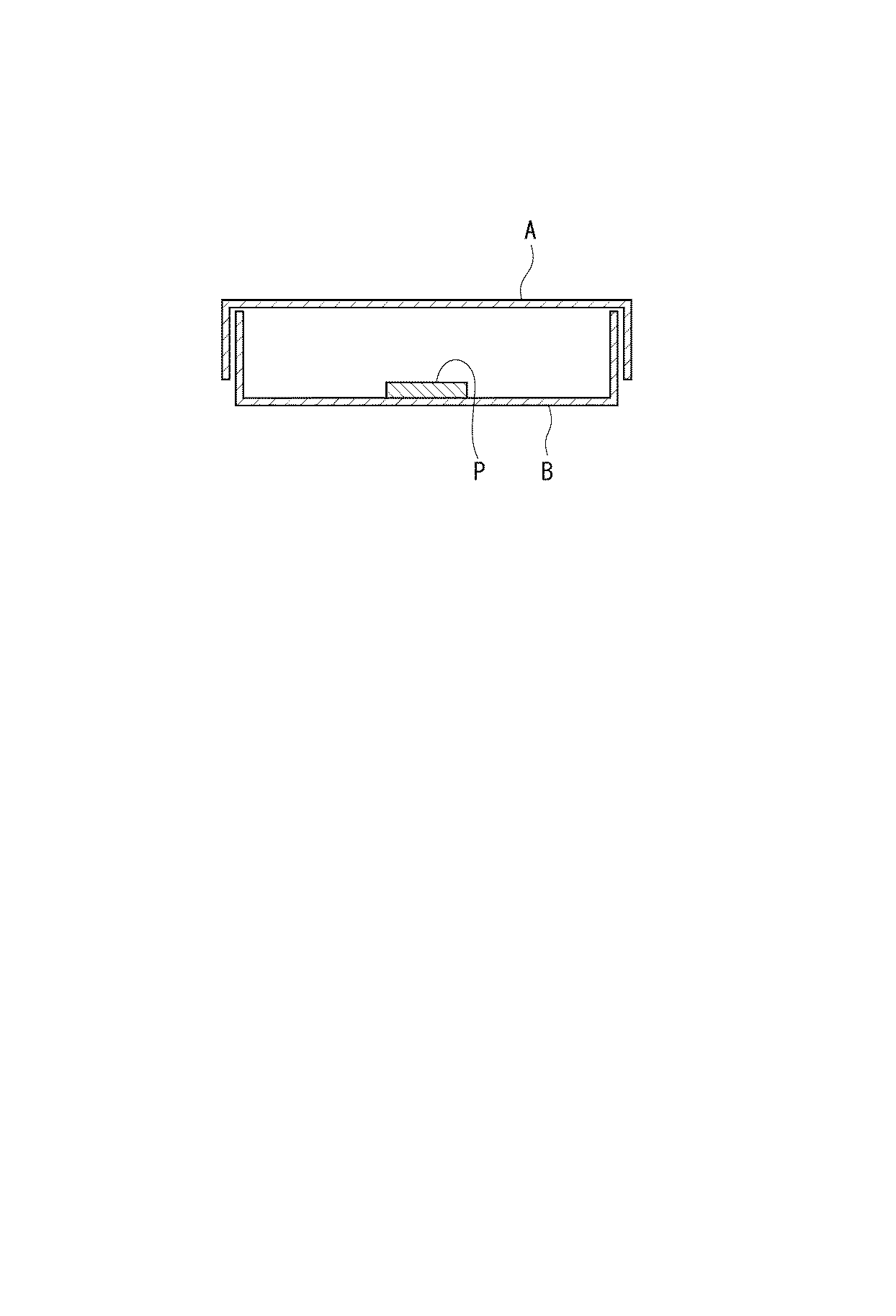
表1に示す結果からも明らかなように、本発明のはんだ組成物を用いた場合(実施例1〜3)には、スズメッキへのはんだぬれ性が優れ、かつはんだ付け部分での腐食を十分に抑制できることが確認された。なお、本発明のはんだ組成物は、加熱時のダレ幅が比較的に大きい傾向にあり、それによりはんだ溶融時のスズメッキへのはんだぬれ性が向上したことが確認された。
これに対し、はんだ組成物の組成において、(A1)成分を含まない場合(比較例1〜6)には、スズメッキ基板へのぬれ広がりが不十分であり、しかもはんだ付け部分での腐食を十分に抑制できないことが分かった。
As is apparent from the results shown in Table 1, when the solder composition of the present invention is used (Examples 1 to 3), the solder wettability to the tin plating is excellent, and corrosion at the soldered portion is sufficient. It was confirmed that it can be suppressed. In addition, it was confirmed that the solder composition of this invention has the tendency for the sagging width | variety at the time of heating to be comparatively large, and, thereby, the solder wettability to the tin plating at the time of solder melting improved.
On the other hand, in the composition of the solder composition, when the component (A1) is not included (Comparative Examples 1 to 6), the wetting and spreading to the tin-plated substrate is insufficient, and corrosion at the soldered portion is sufficient. It was found that it cannot be suppressed.
本発明のはんだ組成物は、電子機器用の筐体などとプリント配線基板などの各種電子部品とのはんだ接合をするための技術や、電子機器のプリント配線基板に部品を実装するための技術や、更には、電子機器用の筐体同士をはんだ接合する技術として好適に用いることができる。 The solder composition of the present invention includes a technique for soldering a casing for electronic equipment and various electronic components such as a printed wiring board, a technique for mounting parts on a printed wiring board for electronic equipment, Furthermore, it can be suitably used as a technique for soldering together casings for electronic devices.
Claims (3)
前記(A)成分は、(A1)軟化点が100℃以下の低軟化点ロジン系樹脂および(A2)軟化点が100℃超の高軟化点ロジン系樹脂を含有し、
前記(A1)成分の配合量は、前記(A1)成分および前記(A2)成分の合計量100質量部に対して、10質量部以上35質量部以下であり、
前記(A)成分の配合量は、フラックス100質量%に対して、30質量%以上70質量%以下であり、
前記(B)成分の配合量は、フラックス100質量%に対して、1質量%以上10質量%以下であり、
前記(C)成分の配合量は、フラックス100質量%に対して、10質量%以上50質量%以下であり、
前記(D)成分の配合量は、フラックス100質量%に対して、0.1質量%以上5質量%以下である
ことを特徴とするはんだ組成物。 (A) a rosin resin, (B) an activator, (C) a solvent and a flux containing (D) an imidazole compound, and (E) a solder powder,
Wherein component (A) contains the (A1) low softening point rosin resin softening point of 100 ° C. or less and (A2) a softening point of 100 ° C. than high softening rosin resin,
The blending amount of the component (A1) is 10 parts by mass or more and 35 parts by mass or less with respect to 100 parts by mass of the total amount of the component (A1) and the component (A2).
The blending amount of the component (A) is 30% by mass to 70% by mass with respect to 100% by mass of the flux,
The blending amount of the component (B) is 1% by mass to 10% by mass with respect to 100% by mass of the flux,
The blending amount of the component (C) is 10% by mass to 50% by mass with respect to 100% by mass of the flux,
A blending amount of the component (D) is 0.1% by mass or more and 5% by mass or less with respect to 100% by mass of the flux .
前記(A1)成分の配合量は、前記(A1)成分および前記(A2)成分の合計量100質量部に対して、10質量部以上25質量部以下であるThe compounding amount of the component (A1) is 10 parts by mass or more and 25 parts by mass or less with respect to 100 parts by mass of the total amount of the component (A1) and the component (A2).
ことを特徴とするはんだ組成物。The solder composition characterized by the above-mentioned.
スズメッキが施された被処理物に用いる
ことを特徴とするはんだ組成物。 In the solder composition according to claim 1 or 2 ,
A solder composition characterized by being used for an object to be treated with tin plating.
Priority Applications (3)
| Application Number | Priority Date | Filing Date | Title |
|---|---|---|---|
| JP2013271690A JP5887331B2 (en) | 2013-12-27 | 2013-12-27 | Solder composition |
| KR1020140187859A KR102181112B1 (en) | 2013-12-27 | 2014-12-24 | Solder composition |
| CN201410828708.6A CN104741833A (en) | 2013-12-27 | 2014-12-26 | Solder composition |
Applications Claiming Priority (1)
| Application Number | Priority Date | Filing Date | Title |
|---|---|---|---|
| JP2013271690A JP5887331B2 (en) | 2013-12-27 | 2013-12-27 | Solder composition |
Publications (2)
| Publication Number | Publication Date |
|---|---|
| JP2015123491A JP2015123491A (en) | 2015-07-06 |
| JP5887331B2 true JP5887331B2 (en) | 2016-03-16 |
Family
ID=53534620
Family Applications (1)
| Application Number | Title | Priority Date | Filing Date |
|---|---|---|---|
| JP2013271690A Active JP5887331B2 (en) | 2013-12-27 | 2013-12-27 | Solder composition |
Country Status (3)
| Country | Link |
|---|---|
| JP (1) | JP5887331B2 (en) |
| KR (1) | KR102181112B1 (en) |
| CN (1) | CN104741833A (en) |
Families Citing this family (16)
| Publication number | Priority date | Publication date | Assignee | Title |
|---|---|---|---|---|
| JP6569905B2 (en) * | 2014-11-21 | 2019-09-04 | 荒川化学工業株式会社 | Flux for screen printing |
| JP6310893B2 (en) * | 2015-09-30 | 2018-04-11 | 株式会社タムラ製作所 | Flux composition, solder composition, and method for manufacturing electronic substrate |
| JP6296663B2 (en) * | 2015-12-04 | 2018-03-20 | 株式会社タムラ製作所 | Flux composition, solder paste composition, and electronic circuit board |
| JP6402148B2 (en) * | 2016-08-31 | 2018-10-10 | 株式会社タムラ製作所 | Solder composition and electronic substrate |
| JP7150232B2 (en) | 2017-07-03 | 2022-10-11 | 株式会社弘輝 | Flux, flux cored solder and solder paste |
| JP6674982B2 (en) * | 2017-08-30 | 2020-04-01 | 株式会社タムラ製作所 | Solder composition and electronic substrate |
| US10913132B2 (en) * | 2017-08-30 | 2021-02-09 | Tamura Corporation | Solder composition, electronic board, and bonding method |
| JP6826059B2 (en) * | 2018-01-31 | 2021-02-03 | 株式会社タムラ製作所 | Flux composition, solder composition and electronic substrate |
| JP6684372B2 (en) * | 2018-03-29 | 2020-04-22 | 株式会社タムラ製作所 | Solder composition for dispensing application |
| JP6849923B2 (en) * | 2018-07-27 | 2021-03-31 | 千住金属工業株式会社 | Solder paste |
| CN109834405B (en) * | 2019-03-22 | 2022-04-26 | 杨小荣 | Solder paste without electrochemical corrosion, preparation method and application thereof |
| JP6681567B1 (en) * | 2019-05-27 | 2020-04-15 | 千住金属工業株式会社 | Solder paste and flux |
| JP6681566B1 (en) * | 2019-05-27 | 2020-04-15 | 千住金属工業株式会社 | Solder paste and flux |
| JP6967050B2 (en) * | 2019-09-27 | 2021-11-17 | 株式会社タムラ製作所 | Flux composition for soldering |
| CN112059467A (en) * | 2020-09-22 | 2020-12-11 | 深圳市鑫富锦新材料有限公司 | Lead-free solder alloy soldering paste |
| JP7450318B2 (en) | 2021-09-16 | 2024-03-15 | 株式会社タムラ製作所 | Solder composition and method for manufacturing flexible circuit board |
Family Cites Families (12)
| Publication number | Priority date | Publication date | Assignee | Title |
|---|---|---|---|---|
| JPH0929486A (en) * | 1995-07-24 | 1997-02-04 | Matsushita Electric Ind Co Ltd | Cream solder |
| JP3892190B2 (en) * | 1999-12-03 | 2007-03-14 | 株式会社日立製作所 | Mixed mounting structure, mixed mounting method, and electronic device |
| JP2003001487A (en) * | 2001-06-15 | 2003-01-08 | Showa Denko Kk | Soldering flux |
| EP1308484A1 (en) * | 2001-10-30 | 2003-05-07 | Sigma Coatings B.V. | Use of silylesters of rosin in self-polishing antifouling paints |
| JP2003264367A (en) * | 2002-03-11 | 2003-09-19 | Tamura Kaken Co Ltd | Reflow soldering solder paste composition and circuit substrate |
| JP4733468B2 (en) * | 2005-08-22 | 2011-07-27 | ローム・アンド・ハース・エレクトロニック・マテリアルズ,エル.エル.シー. | Metal surface treatment aqueous solution and method for preventing discoloration of metal surface |
| US8076407B2 (en) * | 2008-02-08 | 2011-12-13 | Henkel Ag & Co. Kgaa | Hot melt adhesive |
| JP5330460B2 (en) * | 2011-07-04 | 2013-10-30 | 住友ゴム工業株式会社 | High damping composition |
| CN102371443B (en) * | 2011-09-06 | 2017-03-15 | 云南锡业锡材有限公司 | It is applied to scaling powder of multiple tinbase solder(ing) pastes and preparation method thereof |
| CN102489898B (en) * | 2011-11-30 | 2013-07-31 | 昆山成利焊锡制造有限公司 | Low-silver lead-free flux paste and preparation method thereof |
| CN102489899B (en) * | 2011-12-16 | 2013-07-31 | 昆山成利焊锡制造有限公司 | Lead-free soldering paste and preparation method thereof |
| JP5667101B2 (en) * | 2012-02-20 | 2015-02-12 | 株式会社タムラ製作所 | Solder composition, method for producing the same, and printed wiring board |
-
2013
- 2013-12-27 JP JP2013271690A patent/JP5887331B2/en active Active
-
2014
- 2014-12-24 KR KR1020140187859A patent/KR102181112B1/en active Active
- 2014-12-26 CN CN201410828708.6A patent/CN104741833A/en active Pending
Also Published As
| Publication number | Publication date |
|---|---|
| KR20150077344A (en) | 2015-07-07 |
| KR102181112B1 (en) | 2020-11-20 |
| JP2015123491A (en) | 2015-07-06 |
| CN104741833A (en) | 2015-07-01 |
Similar Documents
| Publication | Publication Date | Title |
|---|---|---|
| JP5887331B2 (en) | Solder composition | |
| JP6138464B2 (en) | Solder composition for laser soldering and mounting method using the same | |
| JP6310894B2 (en) | Solder composition and method for producing electronic substrate | |
| JP6674982B2 (en) | Solder composition and electronic substrate | |
| JP6402213B2 (en) | Solder composition and electronic substrate | |
| CN106825994B (en) | Solder composition and electronic substrate | |
| JP6635986B2 (en) | Solder composition and electronic substrate | |
| JP6138846B2 (en) | Solder composition and method for producing electronic substrate using the same | |
| JP5916674B2 (en) | Solder composition for jet dispenser | |
| JP6346757B2 (en) | Method for manufacturing printed wiring board | |
| JP6684372B2 (en) | Solder composition for dispensing application | |
| JP6293514B2 (en) | Solder composition and printed wiring board manufacturing method | |
| JP6402148B2 (en) | Solder composition and electronic substrate | |
| JP6713027B2 (en) | Solder composition and electronic substrate | |
| JP2015131336A (en) | Solder composition and printed wiring board prepared using the same | |
| JP2020055035A (en) | Solder composition and electronic substrate | |
| JP6826059B2 (en) | Flux composition, solder composition and electronic substrate | |
| CN113453445A (en) | Solder composition for laser welding, electronic substrate, and method for producing electronic substrate | |
| JP7361481B2 (en) | Solder composition and electronic board manufacturing method | |
| CN109420861B (en) | Solder composition, electronic substrate, and bonding method | |
| JP7634044B2 (en) | Solder composition and electronic board | |
| CN109719422B (en) | Solder composition and electronic substrate | |
| JP7066798B2 (en) | Solder composition | |
| JP7692313B2 (en) | Flux composition, solder composition and electronic board | |
| JP7554218B2 (en) | Solder composition and electronic substrate |
Legal Events
| Date | Code | Title | Description |
|---|---|---|---|
| A977 | Report on retrieval |
Free format text: JAPANESE INTERMEDIATE CODE: A971007 Effective date: 20151021 |
|
| A131 | Notification of reasons for refusal |
Free format text: JAPANESE INTERMEDIATE CODE: A131 Effective date: 20151110 |
|
| A521 | Written amendment |
Free format text: JAPANESE INTERMEDIATE CODE: A523 Effective date: 20151218 |
|
| TRDD | Decision of grant or rejection written | ||
| A01 | Written decision to grant a patent or to grant a registration (utility model) |
Free format text: JAPANESE INTERMEDIATE CODE: A01 Effective date: 20160202 |
|
| A61 | First payment of annual fees (during grant procedure) |
Free format text: JAPANESE INTERMEDIATE CODE: A61 Effective date: 20160215 |
|
| R150 | Certificate of patent or registration of utility model |
Ref document number: 5887331 Country of ref document: JP Free format text: JAPANESE INTERMEDIATE CODE: R150 |