JP5873907B2 - Illumination apparatus, image sensor unit, image reading apparatus, and image forming apparatus - Google Patents
Illumination apparatus, image sensor unit, image reading apparatus, and image forming apparatus Download PDFInfo
- Publication number
- JP5873907B2 JP5873907B2 JP2014172693A JP2014172693A JP5873907B2 JP 5873907 B2 JP5873907 B2 JP 5873907B2 JP 2014172693 A JP2014172693 A JP 2014172693A JP 2014172693 A JP2014172693 A JP 2014172693A JP 5873907 B2 JP5873907 B2 JP 5873907B2
- Authority
- JP
- Japan
- Prior art keywords
- light
- light guide
- guide member
- image sensor
- light source
- Prior art date
- Legal status (The legal status is an assumption and is not a legal conclusion. Google has not performed a legal analysis and makes no representation as to the accuracy of the status listed.)
- Active
Links
- 238000005286 illumination Methods 0.000 title claims description 7
- 238000003780 insertion Methods 0.000 claims description 24
- 230000037431 insertion Effects 0.000 claims description 24
- 239000000758 substrate Substances 0.000 claims description 19
- 230000000052 comparative effect Effects 0.000 description 9
- 210000000078 claw Anatomy 0.000 description 8
- 238000009792 diffusion process Methods 0.000 description 7
- 230000002093 peripheral effect Effects 0.000 description 7
- 238000000034 method Methods 0.000 description 6
- 239000011521 glass Substances 0.000 description 5
- 230000008602 contraction Effects 0.000 description 4
- 239000000463 material Substances 0.000 description 4
- 239000011347 resin Substances 0.000 description 4
- 229920005989 resin Polymers 0.000 description 4
- 239000006059 cover glass Substances 0.000 description 3
- 238000010586 diagram Methods 0.000 description 3
- 230000003287 optical effect Effects 0.000 description 3
- 229920000515 polycarbonate Polymers 0.000 description 3
- 239000004417 polycarbonate Substances 0.000 description 3
- 230000000903 blocking effect Effects 0.000 description 2
- 238000003384 imaging method Methods 0.000 description 2
- 239000000976 ink Substances 0.000 description 2
- 230000000149 penetrating effect Effects 0.000 description 2
- 239000004925 Acrylic resin Substances 0.000 description 1
- 229920000178 Acrylic resin Polymers 0.000 description 1
- NIXOWILDQLNWCW-UHFFFAOYSA-N acrylic acid group Chemical group C(C=C)(=O)O NIXOWILDQLNWCW-UHFFFAOYSA-N 0.000 description 1
- 239000000853 adhesive Substances 0.000 description 1
- 238000003491 array Methods 0.000 description 1
- 230000002238 attenuated effect Effects 0.000 description 1
- 238000006243 chemical reaction Methods 0.000 description 1
- 239000011248 coating agent Substances 0.000 description 1
- 238000000576 coating method Methods 0.000 description 1
- 230000007423 decrease Effects 0.000 description 1
- 239000000428 dust Substances 0.000 description 1
- 238000005259 measurement Methods 0.000 description 1
- 238000012545 processing Methods 0.000 description 1
- 230000001902 propagating effect Effects 0.000 description 1
- 238000011084 recovery Methods 0.000 description 1
- 230000000717 retained effect Effects 0.000 description 1
- 238000012546 transfer Methods 0.000 description 1
- 239000012780 transparent material Substances 0.000 description 1
Images


Classifications
-
- G—PHYSICS
- G01—MEASURING; TESTING
- G01J—MEASUREMENT OF INTENSITY, VELOCITY, SPECTRAL CONTENT, POLARISATION, PHASE OR PULSE CHARACTERISTICS OF INFRARED, VISIBLE OR ULTRAVIOLET LIGHT; COLORIMETRY; RADIATION PYROMETRY
- G01J1/00—Photometry, e.g. photographic exposure meter
- G01J1/02—Details
- G01J1/04—Optical or mechanical part supplementary adjustable parts
- G01J1/0407—Optical elements not provided otherwise, e.g. manifolds, windows, holograms, gratings
-
- G—PHYSICS
- G02—OPTICS
- G02B—OPTICAL ELEMENTS, SYSTEMS OR APPARATUS
- G02B6/00—Light guides; Structural details of arrangements comprising light guides and other optical elements, e.g. couplings
- G02B6/0001—Light guides; Structural details of arrangements comprising light guides and other optical elements, e.g. couplings specially adapted for lighting devices or systems
- G02B6/0096—Light guides; Structural details of arrangements comprising light guides and other optical elements, e.g. couplings specially adapted for lighting devices or systems the lights guides being of the hollow type
-
- G—PHYSICS
- G02—OPTICS
- G02B—OPTICAL ELEMENTS, SYSTEMS OR APPARATUS
- G02B6/00—Light guides; Structural details of arrangements comprising light guides and other optical elements, e.g. couplings
- G02B6/0001—Light guides; Structural details of arrangements comprising light guides and other optical elements, e.g. couplings specially adapted for lighting devices or systems
- G02B6/0005—Light guides; Structural details of arrangements comprising light guides and other optical elements, e.g. couplings specially adapted for lighting devices or systems the light guides being of the fibre type
- G02B6/0006—Coupling light into the fibre
-
- G—PHYSICS
- G02—OPTICS
- G02B—OPTICAL ELEMENTS, SYSTEMS OR APPARATUS
- G02B6/00—Light guides; Structural details of arrangements comprising light guides and other optical elements, e.g. couplings
- G02B6/0001—Light guides; Structural details of arrangements comprising light guides and other optical elements, e.g. couplings specially adapted for lighting devices or systems
- G02B6/0005—Light guides; Structural details of arrangements comprising light guides and other optical elements, e.g. couplings specially adapted for lighting devices or systems the light guides being of the fibre type
- G02B6/001—Light guides; Structural details of arrangements comprising light guides and other optical elements, e.g. couplings specially adapted for lighting devices or systems the light guides being of the fibre type the light being emitted along at least a portion of the lateral surface of the fibre
-
- H—ELECTRICITY
- H04—ELECTRIC COMMUNICATION TECHNIQUE
- H04N—PICTORIAL COMMUNICATION, e.g. TELEVISION
- H04N1/00—Scanning, transmission or reproduction of documents or the like, e.g. facsimile transmission; Details thereof
- H04N1/024—Details of scanning heads ; Means for illuminating the original
- H04N1/02418—Details of scanning heads ; Means for illuminating the original for picture information pick up and reproduction
-
- H—ELECTRICITY
- H04—ELECTRIC COMMUNICATION TECHNIQUE
- H04N—PICTORIAL COMMUNICATION, e.g. TELEVISION
- H04N1/00—Scanning, transmission or reproduction of documents or the like, e.g. facsimile transmission; Details thereof
- H04N1/024—Details of scanning heads ; Means for illuminating the original
- H04N1/028—Details of scanning heads ; Means for illuminating the original for picture information pick-up
- H04N1/02815—Means for illuminating the original, not specific to a particular type of pick-up head
- H04N1/0282—Using a single or a few point light sources, e.g. a laser diode
- H04N1/02835—Using a single or a few point light sources, e.g. a laser diode in combination with a light guide, e.g. optical fibre, glass plate
-
- H—ELECTRICITY
- H04—ELECTRIC COMMUNICATION TECHNIQUE
- H04N—PICTORIAL COMMUNICATION, e.g. TELEVISION
- H04N1/00—Scanning, transmission or reproduction of documents or the like, e.g. facsimile transmission; Details thereof
- H04N1/024—Details of scanning heads ; Means for illuminating the original
- H04N1/028—Details of scanning heads ; Means for illuminating the original for picture information pick-up
- H04N1/02815—Means for illuminating the original, not specific to a particular type of pick-up head
- H04N1/02885—Means for compensating spatially uneven illumination, e.g. an aperture arrangement
- H04N1/0289—Light diffusing elements, e.g. plates or filters
-
- H—ELECTRICITY
- H04—ELECTRIC COMMUNICATION TECHNIQUE
- H04N—PICTORIAL COMMUNICATION, e.g. TELEVISION
- H04N2201/00—Indexing scheme relating to scanning, transmission or reproduction of documents or the like, and to details thereof
- H04N2201/0077—Types of the still picture apparatus
- H04N2201/0081—Image reader
-
- H—ELECTRICITY
- H04—ELECTRIC COMMUNICATION TECHNIQUE
- H04N—PICTORIAL COMMUNICATION, e.g. TELEVISION
- H04N2201/00—Indexing scheme relating to scanning, transmission or reproduction of documents or the like, and to details thereof
- H04N2201/0077—Types of the still picture apparatus
- H04N2201/0094—Multifunctional device, i.e. a device capable of all of reading, reproducing, copying, facsimile transception, file transception
-
- H—ELECTRICITY
- H04—ELECTRIC COMMUNICATION TECHNIQUE
- H04N—PICTORIAL COMMUNICATION, e.g. TELEVISION
- H04N2201/00—Indexing scheme relating to scanning, transmission or reproduction of documents or the like, and to details thereof
- H04N2201/024—Indexing scheme relating to scanning, transmission or reproduction of documents or the like, and to details thereof deleted
- H04N2201/02452—Arrangements for mounting or supporting elements within a scanning head
- H04N2201/02454—Element mounted or supported
- H04N2201/02456—Scanning element, e.g. CCD array, photodetector
-
- H—ELECTRICITY
- H04—ELECTRIC COMMUNICATION TECHNIQUE
- H04N—PICTORIAL COMMUNICATION, e.g. TELEVISION
- H04N2201/00—Indexing scheme relating to scanning, transmission or reproduction of documents or the like, and to details thereof
- H04N2201/024—Indexing scheme relating to scanning, transmission or reproduction of documents or the like, and to details thereof deleted
- H04N2201/02452—Arrangements for mounting or supporting elements within a scanning head
- H04N2201/02454—Element mounted or supported
- H04N2201/02462—Illuminating means
-
- H—ELECTRICITY
- H04—ELECTRIC COMMUNICATION TECHNIQUE
- H04N—PICTORIAL COMMUNICATION, e.g. TELEVISION
- H04N2201/00—Indexing scheme relating to scanning, transmission or reproduction of documents or the like, and to details thereof
- H04N2201/024—Indexing scheme relating to scanning, transmission or reproduction of documents or the like, and to details thereof deleted
- H04N2201/02493—Additional optical elements not otherwise provided for, e.g. filters, polarising plates, masks or apertures
-
- H—ELECTRICITY
- H04—ELECTRIC COMMUNICATION TECHNIQUE
- H04N—PICTORIAL COMMUNICATION, e.g. TELEVISION
- H04N2201/00—Indexing scheme relating to scanning, transmission or reproduction of documents or the like, and to details thereof
- H04N2201/024—Indexing scheme relating to scanning, transmission or reproduction of documents or the like, and to details thereof deleted
- H04N2201/02497—Additional elements, e.g. sheet guide plates, light shields
Description
本発明は、照明装置、イメージセンサユニット、画像読取装置および画像形成装置に関する。 The present invention relates to an illumination device, an image sensor unit, an image reading device, and an image forming device.
光源、導光体などを有するイメージセンサユニットなどが知られている。特許文献1には、導光体の長手方向における自由端を覆う位置に遮光部材を滑動自在に遊挿したイメージセンサユニットが開示されている。特許文献1のイメージセンサユニットは、雰囲気温度などにより導光体が伸縮した場合であっても、導光体の自由端と光源との間から原稿に向かって直接、照射される漏れ光を遮光部材が遮光することで、漏れ光の発生を防止することができるものである。 An image sensor unit having a light source, a light guide and the like is known. Patent Document 1 discloses an image sensor unit in which a light shielding member is slidably inserted in a position covering a free end in a longitudinal direction of a light guide. The image sensor unit of Patent Document 1 blocks leakage light that is directly irradiated toward the document from between the free end of the light guide and the light source, even when the light guide expands and contracts due to an ambient temperature or the like. Occurrence of leakage light can be prevented by the light shielding of the member.
しかしながら、上述したイメージセンサユニットの遮光部材は光源から原稿に向かって照射される漏れ光を遮光できるものの、遮光部材内に入射されて遮光部材の内面に直接、正反射された光が自由端側から漏れてしまう場合があった。特に、導光体が伸張した場合に比べて収縮した場合には遮光部材の内面が露出されるために、遮光部材の内面に直接、正反射される光が増え、漏れ光がより多く発生していた。したがって、雰囲気温度により導光体の伸縮に応じて漏れ光が変動してしまうために、原稿に照明される照度の均一化を図ることが困難であった。 However, although the light shielding member of the image sensor unit described above can shield the leakage light emitted from the light source toward the document, the light that is incident on the light shielding member and directly reflected directly on the inner surface of the light shielding member is on the free end side. There was a case of leaking from. In particular, when the light guide is contracted compared to when it is stretched, the inner surface of the light shielding member is exposed, so that the amount of light that is directly reflected directly on the inner surface of the light shielding member increases and more light leaks. It was. Therefore, the leakage light varies according to the expansion and contraction of the light guide depending on the ambient temperature, and it is difficult to make the illuminance illuminated on the original uniform.
本発明は、上述したような問題点に鑑みてなされたものであり、導光部材が伸縮した場合であっても被照明体に照明される照度の均一化を図ることを目的とする。 The present invention has been made in view of the above-described problems, and an object of the present invention is to make the illuminance illuminated on the illuminated body uniform even when the light guide member expands and contracts.
本発明の照明装置は、被照明体をライン状に照明する照明装置であって、第1の光源と、第2の光源と、前記第1の光源が長手方向の一方の端部、前記第2の光源が長手方向の他方の端部に配置され、前記第1の光源および前記第2の光源から発光された光を反射面により伝搬させながら出射面から前記被照明体に出射させ、前記一方の端部を固定端とし前記他方の端部を自由端とする棒状の導光部材と、前記導光部材の前記他方の端部を摺動可能に覆う包囲部を有する遮光部材と、を備え、前記包囲部は、前記導光部材の前記一方の端部側に突出され前記導光部材の前記出射面を覆う遮光部と、前記遮光部に隣接して前記導光部材の反射面の一部を露出させる切り欠き部と、を有することを特徴とする。
本発明のイメージセンサユニットは、上述した照明装置と、前記被照明体からの反射光を結像する集光体と、前記集光体によって結像された光を受光して電気信号に変換するイメージセンサと、を有することを特徴とする。
本発明の画像読取装置は、上述したイメージセンサユニットと、前記イメージセンサユニットと前記被照明体とを相対的に移動させる移動部と、を有することを特徴とする。
本発明の画像形成装置は、上述したイメージセンサユニットと、前記イメージセンサユニットと前記被照明体とを相対的に移動させる移動部と、前記イメージセンサユニットにより読み取られた画像を記録媒体に形成する画像形成部と、を有することを特徴とする。
The illuminating device of the present invention is an illuminating device that illuminates an object to be illuminated in a line shape, wherein the first light source, the second light source, the first light source has one end in the longitudinal direction, Two light sources are arranged at the other end in the longitudinal direction, and the light emitted from the first light source and the second light source is emitted from the emission surface to the illuminated body while propagating through the reflection surface, A rod-shaped light guide member having one end portion as a fixed end and the other end portion as a free end; and a light-shielding member having a surrounding portion that slidably covers the other end portion of the light guide member. The surrounding portion includes a light shielding portion that protrudes toward the one end portion of the light guide member and covers the emission surface of the light guide member, and a reflective surface of the light guide member adjacent to the light shielding portion. It has a notch part which exposes a part, It is characterized by the above-mentioned.
An image sensor unit according to the present invention receives the above-described illumination device, a light collector that forms an image of reflected light from the object to be illuminated, and the light imaged by the light collector and converts it into an electrical signal. And an image sensor.
An image reading apparatus according to the present invention includes the above-described image sensor unit, and a moving unit that relatively moves the image sensor unit and the object to be illuminated.
The image forming apparatus of the present invention forms the image sensor unit described above, a moving unit that relatively moves the image sensor unit and the object to be illuminated, and an image read by the image sensor unit on a recording medium. And an image forming unit.
本発明によれば、導光部材が伸縮した場合であっても被照明体に照明される照度の均一化を図ることができる。 According to the present invention, even when the light guide member expands and contracts, the illuminance illuminated on the illuminated body can be made uniform.
以下、本発明を適用できる実施形態について、図面を参照して詳細に説明する。本実施形態は、照明装置と、この照明装置が適用されるイメージセンサユニット10と、このイメージセンサユニット10が適用される画像読取装置および画像形成装置である。画像読取装置および画像形成装置では、イメージセンサユニット10が被照明体としての原稿Pに光を照射し、反射光を電気信号に変換することで画像を読み取る。
以下の説明においては、三次元の各方向を、X,Y,Zの各矢印で示す。X方向が主走査方向であり、Y方向が主走査方向に直角な副走査方向であり、Z方向が垂直方向(上下方向)である。
Hereinafter, embodiments to which the present invention can be applied will be described in detail with reference to the drawings. The present embodiment is an illumination device, an
In the following description, three-dimensional directions are indicated by X, Y, and Z arrows. The X direction is the main scanning direction, the Y direction is the sub scanning direction perpendicular to the main scanning direction, and the Z direction is the vertical direction (up and down direction).
(第1の実施形態)
まず、本実施形態に係る画像読取装置または画像形成装置の一例である多機能プリンタ(MFP;Multi Function Printer)の構造について図2を参照して説明する。図2は、MFP100の外観を示す斜視図である。図2に示すように、MFP100は、原稿Pからの反射光を読み取る画像読取手段としての画像読取部102と、記録媒体としてのシート101(記録紙)に原稿Pの画像を形成(印刷)する画像形成手段としての画像形成部113とを備えている。
(First embodiment)
First, the structure of a multi-function printer (MFP) that is an example of an image reading apparatus or an image forming apparatus according to the present embodiment will be described with reference to FIG. FIG. 2 is a perspective view showing an appearance of
画像読取部102はいわゆるイメージスキャナーの機能を有するものであり、例えば以下のように構成される。画像読取部102は、筐体103と、原稿載置部としてのガラス製の透明板からなるプラテンガラス104と、原稿Pを覆うことができるように筐体103に対して開閉自在に設けられるプラテンカバー105とを備えている。
筐体103の内部には、照明装置を備えたイメージセンサユニット10、保持部材106、イメージセンサユニットスライドシャフト107、イメージセンサユニット駆動モータ108、ワイヤ109、信号処理部110、回収ユニット111、給紙トレイ112などが収納されている。
The
Inside the
イメージセンサユニット10は、例えば密着型イメージセンサ(CIS;Contact Image Sensor)ユニットである。保持部材106は、イメージセンサユニット10を囲むように保持する。イメージセンサユニットスライドシャフト107は、保持部材106をプラテンガラス104に沿って副走査方向に案内する。イメージセンサユニット駆動モータ108は、イメージセンサユニット10と原稿Pとを相対的に移動させる移動部であり、具体的には保持部材106に取り付けられたワイヤ109を動かす。回収ユニット111は筐体103に対して開閉自在に設けられ、印刷されたシート101を回収する。給紙トレイ112は、所定のサイズのシート101を収容する。
The
上述したように構成される画像読取部102では、イメージセンサユニット駆動モータ108がイメージセンサユニットスライドシャフト107に沿ってイメージセンサユニット10を副走査方向に移動させる。この際、イメージセンサユニット10はプラテンガラス104上に載置された原稿Pを光学的に読み取って、電気信号に変換することで、画像の読み取り動作を行う。
In the
図3は画像形成部113の構造を示す概略図である。
画像形成部113はいわゆるプリンタの機能を有するものであり、例えば以下のように構成される。画像形成部113は筐体103内部に収容されており、図3に示すように、搬送ローラ114と、記録ヘッド115とを備えている。記録ヘッド115は、例えばシアンC、マゼンタM、イエローY、黒Kのインクを備えたインクタンク116(116c,116m,116y,116k)と、これらのインクタンク116にそれぞれ設けられた吐出ヘッド117(117c,117m,117y,117k)から構成される。また、画像形成部113は、記録ヘッドスライドシャフト118、記録ヘッド駆動モータ119、記録ヘッド115に取り付けられたベルト120を有している。
FIG. 3 is a schematic view showing the structure of the
The
上述したように構成される画像形成部113では、給紙トレイ112から供給されたシート101は、搬送ローラ114によって記録位置まで搬送される。記録ヘッド115は、記録ヘッド駆動モータ119によりベルト120を機械的に動かすことで、記録ヘッドスライドシャフト118に沿って印刷方向(主走査方向)に移動しつつ電気信号を基にシート101に対して印刷を行う。印刷終了まで上述した動作を繰り返した後、印刷されたシート101は搬送ローラ114によって回収ユニット111に排出される。
なお、画像形成部113としてインクジェット方式による画像形成装置を説明したが、電子写真方式、熱転写方式、ドットインパクト方式などどのような方式であっても構わない。
In the
Although an image forming apparatus using an inkjet method has been described as the
次に、本実施形態のイメージセンサユニット10について図面を参照して説明する。図4は、イメージセンサユニット10の斜視図である。図5は、イメージセンサユニット10の分解斜視図である。図6は、イメージセンサユニット10を副走査方向に沿って切断した断面図である。
イメージセンサユニット10は、フレーム11、導光部20、光源50、基板55、集光体58、イメージセンサ60などを備えている。これらの構成部材のうち、導光部20および光源50は、照明装置として機能させることができる。また、上述した構成部材のうち、フレーム11、導光部20、基板55、集光体58、イメージセンサ60は、読み取る原稿Pの主走査方向の寸法に応じた長さに形成されている。
Next, the
The
フレーム11は、イメージセンサユニット10の各構成部材を収容する収容部材である。フレーム11は、主走査方向に長い略直方体であり、内部には各構成部材を位置決めして支持できるように形成されている。図6に示すように、フレーム11の上側の略中央には、集光体58を収容する集光体収容部12が主走査方向に形成されている。また、フレーム11には、集光体収容部12を挟んだ両側には導光部20を収容する導光収容部13が主走査方向に形成されている。導光収容部13内には、後述する連結部45の係合突起17と係合させるための係合部14が主走査方向に間隔をあけて複数形成されている(図5を参照)。また、フレーム11の略中央には、基板55を配置するための基板収容部15が主走査方向に亘ってフレーム11の下側から凹状に形成されている。基板収容部15に収容された基板55は、例えば固定ネジにより固定される。また、フレーム11の主走査方向の両端には、光源50が配置される空間16がフレーム11の上下方向に開口して形成されている(図5を参照)。また、フレーム11は、例えば、黒色に着色された遮光性を有する樹脂材料により形成される。樹脂材料には、例えばポリカーボネートが適用できる。
The
導光部20は、光源50から発光された光をライン状に原稿Pへと導く。
本実施形態のイメージセンサユニット10は、原稿Pに照明される照度を増やすために、2つの導光部20(第1の導光部20a、第2の導光部20b)を有すると共に、1つの導光部20に対して長手方向の両端にそれぞれ光源50が配置される。
第1の導光部20aおよび第2の導光部20bは同一の構成であり、図4に示すイメージセンサユニット10の中心線cと主走査方向に配置された集光体58とが交差する点Oを中心に点対称に配置されている。ここでは、第1の導光部20aを中心に説明する。
The
The
The
図7は、図6のうち第1の導光部20aなどを示した斜視図である。
導光部20aは、導光部材21と遮光部材30とを有し、遮光部材30が導光部材21を保持することで構成されている。
導光部材21は、例えばアクリル系の樹脂などの透明な材料により形成され、主走査方向に長い棒状に形成されている。
導光部材21は、主走査方向の両端部のうち一方の端部に第1の光源50aからの光を入射させる入射面22aが形成され、他方の端部に第2の光源50bからの光を入射させる入射面22bが形成されている。第1の入射面22aおよび第2の入射面22bは、主走査方向に対して直交している。
FIG. 7 is a perspective view showing the
The
The
The
図8は、導光部材21の断面図、正面図および側面図である。導光部材21には、原稿Pと対面する面に導光部材21内に入射された光を原稿Pに向かって出射させる出射面23が形成されている。出射面23は、上側に凸状の円弧状に形成されている。また、導光部材21は、出射面23と対向する面に、入射面22a、22bから入射された光を反射させて導光部材21の長手方向に伝搬させる反射面24が形成されている。反射面24には、複数の拡散部25が長手方向に間隔をあけて形成されている。拡散部25はプリズム形状に形成され、拡散部25に入射された光を反射面24の下側に向かって拡散させる。下側に向かって拡散された光は、後述する遮光部材30の反射面49により反射されることで、導光部材21の出射面23から上側に向かって出射される。
FIG. 8 is a cross-sectional view, a front view, and a side view of the
また、出射面23および反射面24以外の面は、それぞれ入射された光を反射させる反射面として機能する。すなわち、導光部材21には、出射面23の一方側に隣接する反射面26と、他方側に隣接する反射面27と、反射面24と反射面26との間に位置する反射面28とが形成されている。
図7に示すように、導光部材21の一方の端部には、被係止部として係止爪29が一体で形成されている。係止爪29は、反射面27から導光部材21の長手方向に対して直交する方向に突出している。
In addition, the surfaces other than the
As shown in FIG. 7, a locking
遮光部材30は、例えばポリカーボネートなどにより形成され、導光部材21よりも主走査方向に僅かに長く形成されている。遮光部材30は、光の反射率を向上させるために例えば白色に着色されている。
遮光部材30は、一方の端部に形成された第1の包囲部31と、他方の端部に形成された第2の包囲部35と、第1の包囲部31と第2の包囲部35とを繋ぐ連結部45とを有している。
第1の包囲部31は、主走査方向で見たときに外形が略矩形状であって、主走査方向に貫通する挿通孔32を有する略筒状に形成されている。挿通孔32は、導光部材21の断面形状よりも大きな形状であり、導光部材21を挿入可能である。導光部材21が遮光部材30によって保持された状態では、導光部材21の一方の端部は挿通孔32内に位置することで第1の包囲部31によって覆われる。
図9は、第1の包囲部31を図7に示す矢印A方向から見た斜視図である。図9に示すように、第1の包囲部31は、上部の端面から主走査方向に向かって突出する庇部33が形成されている。また、第1の包囲部31には、導光部材21の係止爪29に係止する凹状の係止部34が形成されている。係止部34は、挿通孔32に隣接した位置であって、第1の包囲部31の端面から連続して主走査方向に凹状に形成されている。なお、係止部34は、導光部材21を遮光部材30によって保持させるときに、後述するように導光部材21の挿入方向に沿って形成されている。
The
The
The first surrounding
FIG. 9 is a perspective view of the first surrounding
第2の包囲部35は、主走査方向で見たときに外形が略矩形状であって、主走査方向に貫通する挿通孔36を有する略筒状に形成されている。挿通孔36は、導光部材21の断面形状よりも大きな形状であり、導光部材21を挿入可能である。導光部材21が遮光部材30によって保持された状態では、導光部材21の他方の端部は挿通孔36内に位置することで第2の包囲部35によって覆われる。
図10は、第2の包囲部35の正面図および側面図である。図10では、導光部材21を二点鎖線で示している。第2の包囲部35のうち上部37は導光部材21を上側から覆う。また、側部38および側部39は、導光部材21の反射面26、反射面27を側方から覆う。また、下部40は、導光部材21の反射面24、反射面28を下側から覆う。
The second surrounding
FIG. 10 is a front view and a side view of the second surrounding
第2の包囲部35は、上部37の端面から主走査方向に突出する庇部41が形成されている。庇部41は、第1の包囲部31の庇部33と同一形状である。第2の包囲部35は、上部37から第1の包囲部31側に向かって突出する遮光部42を有している。遮光部42は、導光部材21の出射面23を上側から覆うことで、漏れ光を遮蔽することができる。
遮光部42が形成された領域(図10に示すQ)では、遮光部42に隣接して、第2の包囲部35の側部39が切り欠かれた切り欠き部43が形成されている。したがって、遮光部42が形成された領域では、導光部材21の反射面26および反射面28の一部が露出される。
The second surrounding
In the region where the
連結部45は、断面略U字状であって、主走査方向に沿って導光部材21と略同一の長さに形成されている。具体的には、連結部45は、第2の包囲部35のうち集光体58が配置される側を開口した断面形状である。導光部材21が遮光部材30によって保持された状態では、導光部材21の略半分が連結部45によって覆われる。
図11は、図6に示す導光部20aの拡大図である。図11に示すように、連結部45は、第2の包囲部35のうち遮光部42および側部39を省略した形状である。連結部45のうち上部46は、導光部材21の出射面23の一部を上側から覆うことにより、原稿Pに出射させる光の方向を規制する。また、側部47は、導光部材21の反射面27を側方から覆う。また、下部48は、導光部材21の反射面24を下側から覆う。
The connecting
FIG. 11 is an enlarged view of the
ここで、下部48の内周面の一部は、断面略U字状の開口方向に向かって下側に傾斜する反射面49が形成されている。反射面49は、導光部材21の拡散部25によって下側に向かって拡散された光を導光部材21の出射面23側に反射させる。なお、連結部45の上部46の内周面および側部47の内周面も光を反射させる機能を有している。
また、側部47の外側面には、長手方向に間隔をあけて複数の被係合部としての係合突起17が形成されている。係合突起17はフレーム11の係合部14と係合することで、遮光部材30がフレーム11内で保持される。
Here, a part of the inner peripheral surface of the
Further, on the outer surface of the
導光部材21を遮光部材30によって保持させる場合には、導光部材21の他方の端部を遮光部材30の第1の包囲部31の挿通孔32に挿入した後、連結部45内から、遮光部材30の第2の包囲部35の挿通孔36の順に挿入する。導光部材21の係止爪29が遮光部材30の第1の包囲部31の係止部34に係止するまで、導光部材21を挿入することで、導光部材21が遮光部材30によって保持される。このように、係止部34は導光部材21の挿入方向に沿って形成されている。
When the
光源50は、光を発光することで導光部20を介して原稿Pに光を出射する。光源50には、LEDチップ51が実装されたLEDモジュール52が用いられている。本実施形態は、第1の導光部20aの長手方向の両端に第1の光源50a、第2の光源50bが配置され、第2の導光部20bの長手方向の両端に第3の光源50c、第4の光源50dが配置される。第1の光源50a〜第4の光源50dは、同一の構成であり、以下では、第1の導光部20aの両端に配置される第1の光源50a、第2の光源50bを中心に説明する。
図7に示すように、光源50としてのLEDモジュール52は、表面にLEDチップ51が実装されたいわゆる表面実装型のLEDモジュールである。LEDモジュール52は、略直方体に形成された筐体53を有する。筐体53の表面の一部には凹状に形成され、発光部としてのLEDチップ51が配置されている。ここでは、複数(例えば3つ)のLEDチップ51(51a、51b、51c)が、透明樹脂によって封止された状態で配置されている。LEDチップ51a、51b、51cには、例えば赤、緑および青などの発光波長を有するLEDチップが適用できる。
The
As shown in FIG. 7, the
基板55は、主走査方向に長い平板状に形成される。基板55の実装面56は、上下方向に対して直交している。基板55の実装面56上には、LEDモジュール52を発光させるための駆動回路などが実装されている。
集光体58は、原稿Pからの反射光をイメージセンサ60上に結像する光学部材である。集光体58は、例えば複数の正立等倍結像型の結像素子(ロッドレンズ)が主走査方向に直線状に配列されるロッドレンズアレイが適用できる。集光体58は、フレーム11の集光体収容部12に上側から挿入され、導光収容部13内に保持される。なお、集光体58は、イメージセンサ60上に結像できればよく、上述した構成に限定されない。集光体58には各種マイクロレンズアレイなど、従来公知の各種集光機能を有する光学部材が適用できる。
The
The
イメージセンサ60は、基板55に実装され、集光体58の下側に配置される。図7に示すように、イメージセンサ60は、イメージセンサユニット10の読み取りの解像度に応じた複数の受光素子(受光素子は光電変換素子ということもある)から構成されるイメージセンサIC61の所定数を基板55の実装面56上に主走査方向に直線状に配列して実装される。イメージセンサ60は、原稿Pから反射され集光体58によって結像された反射光を受光して電気信号に変換する。なお、イメージセンサ60は、原稿Pから反射された反射光を電気信号に変換できるものであればよく、上述した構成に限定されない。イメージセンサIC61には、従来公知の各種イメージセンサICが適用できる。
The
上述したように構成されるイメージセンサユニット10の組み立て方法について説明する。まず、イメージセンサ60を予め実装した基板55の長手方向の両端に、第1の光源50a〜第4の光源50dとしてのLEDモジュール52を実装する。
次に、LEDモジュール52が実装された基板55をフレーム11の下側から基板収容部15に挿入して、例えば固定ネジにより固定する。このとき、LEDモジュール52は、フレーム11の空間16内に配置される。次に、集光体58をフレーム11の上側から集光体収容部12に挿入して、例えば接着剤により固定する。また、第1の導光部20aおよび第2の導光部20bをフレーム11の上側から導光収容部13にそれぞれ挿入する。フレーム11の導光収容部13に形成された係合部14が導光部20a、20bの連結部45に形成された係合突起17と係合することにより、導光部20a、導光部20bがフレーム11に保持される。このとき、第1の包囲部31の庇部33および第2の包囲部35の庇部41がそれぞれLEDモジュール52bの筐体53の上部に載置される。
A method for assembling the
Next, the board |
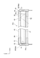
図1は、図4に示すII−II線の断面図(あるいは図11に示すII−II線も参照)であり、導光部20aがフレーム11に保持された状態を示している。
図1に示すように、導光部20aがフレーム11に保持された状態では、導光部材21の入射面22aに第1の光源50aのLEDチップ51が対面し、導光部材21の入射面22bに第2の光源50bのLEDチップ51が対面する。このとき、入射面22bは、第2の光源50bと、切り欠き部43との間に配置される。また、第1の包囲部31が導光部材21の一方の端部を覆い、第2の包囲部35が導光部材21の他方の端部を覆う。
FIG. 1 is a cross-sectional view taken along the line II-II shown in FIG. 4 (or see also the line II-II shown in FIG. 11), and shows a state where the
As shown in FIG. 1, in a state where the
上述したように構成されるイメージセンサユニット10では、光源50を発光させることにより、図6に示すように、第1の導光部20aおよび第2の導光部20bから原稿Pの下面に対して矢印R1、R2に示すように光を出射する。したがって、原稿Pには読取ラインS(主走査方向)に亘ってライン状に光が出射される。この光は原稿Pによって反射されることで、集光体58を介して反射光がイメージセンサ60上に結像される。イメージセンサ60は、結像された反射光を電気信号に変換することで、原稿Pの下面の画像を読み取ることができる。
In the
イメージセンサ60が反射光を1走査ライン分読み取ることで、原稿Pの主走査方向における1走査ラインの読み取り動作を完了する。1走査ラインの読み取り動作終了後、原稿Pの副走査方向への相対的な移動に伴い、上述する動作と同様に次の1走査ライン分の読み取り動作が行われる。このようにイメージセンサユニット10が副走査方向に移動しながら1走査ライン分ずつ読み取り動作を繰り返すことで、原稿Pの全面が順次走査されて反射光により画像の読み取りが行われる。
When the
上述したように構成されるイメージセンサユニット10では、読み取り動作時には高温になり、停止時には室温付近まで冷却される。このとき、導光部材21は、フレーム11あるいは遮光部材30と異なる材料により形成されているために、フレーム11や遮光部材30との間で伸縮率が異なる。具体的には、導光部材21は、フレーム11や遮光部材30よりも伸縮率が大きいため、高温になるほど長手方向に伸張し、低温になるほど長手方向に収縮する。
ここで、導光部材21の一方の端部は係止爪29により遮光部材30に係止されているために固定端となる。したがって、第1の光源50aと入射面22aとの隙間は温度に関わらずほぼ一定である。一方、導光部材21の他方の端部は遮光部材30に係止されていないために自由端となる。したがって、第2の光源50bと入射面22bとの隙間は、導光部材21が伸縮することによって変動する。
In the
Here, since one end portion of the
特に、導光部材21が収縮して、第2の光源50bと入射面22bとの隙間が大きくなった場合には、第2の包囲部35の挿通孔36の内周面が露出される。そのため、従来では、第2の光源50bから発光された光が、挿通孔36の内周面に直接、反射される光が増えて、反射された光が導光部材21の出射面23から原稿Pに向かって出射され、漏れ光として多く発生していた。すなわち、雰囲気温度による導光部材21の伸縮に応じて漏れ光が変動するために、導光部材21から出射され原稿Pに照射される照度を均一化することが困難であった。
そこで、本実施形態では、第2の包囲部35の上部37から第1の包囲部31に向かって突出する遮光部42が形成したことにより、挿通孔36の内周面に反射された光が遮光部42により遮蔽されることから、原稿Pに向かって出射されることを防止することができる。また、遮光部42により遮蔽された光は、遮光部42により反射され、図1に示すように、遮光部42により反射された光の一部が導光部材21内を通って切り欠き部43を通して、導光部20aの下側に出射される。すなわち、導光部20aの下側に出射された光は、フレーム11により減光され、漏れ光の発生を防止することができる。したがって、導光部材21が伸縮した場合であっても、原稿Pに照明される照度を均一化することができる。
In particular, when the
Therefore, in the present embodiment, the light reflected from the inner peripheral surface of the
ここで、比較例として遮光部を形成しない遮光部材を用いたときの光の照度と、実施例として本実施形態の遮光部42を形成した遮光部材30を用いたときの光の照度について解析する。
(比較例)
図12Aは、比較例の遮光部材70の斜視図である。図12Aに示すように、遮光部材70の包囲部(第2の包囲部)71は、本実施形態の遮光部を形成されていないことを除き実施例と同様の形状であり、同一符号を付して説明を省略する。
図13Aは、比較例の遮光部材70の包囲部71と導光部材21との関係を示す断面図である。ここでは、比較例の遮光部材70の包囲部71の主走査方向の寸法tを3mmとする。包囲部71の一方側の端部からの導光部材21の距離L1を変更させたときに、第2の光源50bから主走査方向(x方向)に応じた読取ラインSの照度を測定する。
Here, the illuminance of light when using a light shielding member that does not form a light shielding portion as a comparative example and the illuminance of light when using the
(Comparative example)
FIG. 12A is a perspective view of a
FIG. 13A is a cross-sectional view showing the relationship between the surrounding
図14Aは、測定した照度の結果を示すグラフであり、縦軸が照度[W/mm2]を示
し、横軸が光源50bからの距離x[mm]を示している。また、図14Aにおいて、実線で示す特性線81がL1=0.7mmのときの照度変化であり、破線で示す特性線82がL1=1.7mmのときの照度変化であり、一点鎖線で示す特性線83がL1=2.7mmのときの照度変化である。図14Aに示すように、遮光部を形成しない場合、導光部材21の入射面22bと第2の光源50bとの隙間が大きくなるほど漏れ光が増えてしまい、照度の均一化を図ることができない。
FIG. 14A is a graph showing the results of measured illuminance, where the vertical axis represents illuminance [W / mm 2 ] and the horizontal axis represents distance x [mm] from the
(実施例)
図12Bは、実施例の遮光部材30の斜視図であり、図7に示す矢印B方向から見た図に相当する。遮光部材30は、上述した実施形態と同様の形状であり、同一符号を付して説明を省略する。
図13Bは、実施例の遮光部材30の第2の包囲部35と導光部材21との関係を示す断面図である。ここでは、実施例の遮光部材30の第2の包囲部35のうち遮光部42を除いた主走査方向の寸法tを3mmとし、遮光部42の主走査方向の寸法uを2mmとする。第2の包囲部35の一方側の端部からの導光部材21の距離L2を変更させたときに、第2の光源50bから主走査方向(x方向)に応じた読取ラインSの照度を測定する。
(Example)
12B is a perspective view of the
FIG. 13B is a cross-sectional view illustrating a relationship between the second surrounding
図14Bは、測定した照度の結果を示すグラフであり、縦軸が照度[W/mm2]を示
し、横軸が光源50からの距離x[mm]を示している。また、図14Bにおいて、実線で示す特性線91がL2=0.7mmのときの照度変化であり、破線で示す特性線92がL2=1.7mmのときの照度変化であり、一点鎖線で示す特性線93がL2=2.7mmのときの照度変化である。図14Bに示すように、遮光部42を形成した場合、導光部材21の入射面22bと第2の光源50bとの隙間が大きくなったとしても比較例と比べて漏れ光が増えることがなく、照度の均一化を図ることができる。
FIG. 14B is a graph showing the results of the measured illuminance, where the vertical axis indicates the illuminance [W / mm 2 ] and the horizontal axis indicates the distance x [mm] from the
以上、本実施形態によれば、第2の包囲部35は、導光部材21の一方の端部側に突出し導光部材21の出射面23を覆う遮光部42と、遮光部42に隣接して導光部材21の反射面の一部、具体的には反射面26を露出させる切り欠き部43とを有する。このように構成することで、特に、導光部材21が収縮して第2の光源50bと入射面22bとの隙間が大きくなった場合であっても、第2の光源50bから直接、第2の包囲部35の挿通孔36の内周面によって反射された光を遮光部42によって遮蔽することで原稿Pに出射されることを防止できる。また、遮光部42により遮蔽された光は、遮光部42により反射され、その一部を切り欠き部43を通して逃がすことで、再び原稿Pに出射されることを防止できる。したがって、雰囲気温度によって導光部材21が伸縮した場合であっても、導光部材21から出射されて原稿Pが照明される照度を均一化することができる。
As described above, according to the present embodiment, the second surrounding
また、本実施形態では、切り欠き部43は、出射面23に隣接する反射面26を露出させている。ここで、切り欠き部43が導光部材21の反射面のうち出射面23の対向する反射面24を露出させた場合には、多くの光が切り欠き部43を通して逃げてしまい、導光部材21から出射される光量が低下してしまうおそれがある。そこで、切り欠き部43が出射面23に隣接する反射面26を露出させることで遮光部42により反射された光を適度に逃がし、導光部材21から出射される光量を低下させないようにしている。
In the present embodiment, the
また、本実施形態では、遮光部材30には、導光部材21の一方の端部に形成された係止爪29と係止する係止部34と、導光部材21の出射面23と対向する反射面24を覆う連結部45とが一体で形成されている。したがって、導光部材21と遮光部材30とを組み付けるだけで、導光部材21の一方の端部を固定端となるよう係止され、導光部材21の他方の端部を自由端となるように第2の包囲部35により摺動可能に覆うことができる。
また、本実施形態では、導光部材21が遮光部材30を介してフレーム11に保持されている。したがって、フレーム11の狭い空間内に導光部材21と遮光部材30とを別々に組み付ける必要がないので、組み付けを容易に行うことができる。
In the present embodiment, the
In the present embodiment, the
(第2の実施形態)
次に、第2の実施形態の遮光部材について図15を参照して説明する。なお、第1の実施形態と同様の構成は、同一符号を付してその説明を省略する。
図15は、本実施形態の遮光部材の構成を示す斜視図である。
本実施形態の遮光部材85は、第1の包囲部86が断面略U字状であって、連結部45と同様に集光体58が配置される側を開口した断面形状である。したがって、導光部材21が遮光部材85に保持された状態では、導光部材21の一方の端部の一部のみが第1の包囲部86によって覆われる。具体的には、導光部材21の一方の端部のうち、出射面23の一部および出射面23に隣接する反射面26が露出させる。
(Second Embodiment)
Next, the light shielding member of the second embodiment will be described with reference to FIG. In addition, the same code | symbol is attached | subjected to the structure similar to 1st Embodiment, and the description is abbreviate | omitted.
FIG. 15 is a perspective view showing the configuration of the light shielding member of the present embodiment.
In the
また、第1の包囲部86には、導光部材21の係止爪29に係止する係止部87が形成されている。本実施形態の係止部87は、第1の包囲部86の端面から主走査方向から離れた位置であって、主走査方向に対して直交する方向に沿って形成された孔である。
一方、遮光部材85の第2の包囲部35は、第1の実施形態と同様に挿通孔36が形成されている。したがって、導光部材21を遮光部材85によって保持させる場合、第1の実施形態と異なり、導光部材21の他方の端部を第1の包囲部86ではなく、直接、第2の包囲部35の挿通孔36に挿入する。その後、導光部材21を主走査方向と直交する方向から遮光部材85内に嵌め込むように挿入する。このとき、導光部材21の係止爪29を主走査方向と直交する方向から第1の包囲部86の係止部87の孔に沿って挿入することで、導光部材21が遮光部材85によって保持される。
In addition, the first surrounding
On the other hand, the second surrounding
このように、遮光部材85の第1の包囲部86を主走査方向に対して直交する方向に開口させることで、導光部材21の他方の端部を第2の包囲部35の挿通孔36のみに挿入すればよく、導光部20を容易に組み立てることができる。また、導光部材21の他方の端部を第2の包囲部35の挿通孔36のみに挿入すれば組み立てられるので、導光部材21が挿通孔36に挿入するときに両者が接触してしまう長さを少なくでき、導光部材21が傷付くことを防止することができる。
また、第1の包囲部86に形成された係止部87は、導光部材21を主走査方向と直交する方向から遮光部材85内に嵌め込むときの挿入方向に沿った孔である。この孔により、導光部材21を遮光部材85内に嵌め込むだけで、導光部材21の一方の端部を固定端となるよう係止させることができる。また、係止部87は主走査方向に対して直交する方向に沿って形成された孔であるために、導光部材21の係止爪29を係止部87に係止することで、導光部材21の主走査方向における位置決め精度を向上させることができる。
In this way, by opening the first surrounding
The locking
また、本実施形態の第1の包囲部86は、端面に位置合わせ部88が一体で形成されている。位置合わせ部88は、第1の包囲部86の端面から主走査方向に沿って突出する、例えば複数(2つ)の円柱状の突起89である。位置合わせ部88は、後述する第1の光源95aの回路基板97の被位置合わせ部98に係合される。
Further, the first surrounding
第1の光源95aは、LEDチップ51が配置されたトップビュータイプの表面実装型のLEDパッケージ96が回路基板97上に実装して構成されている。回路基板97は、被位置合わせ部98が形成される。被位置合わせ部98は、例えば複数(2つ)の挿入孔99である。したがって、第1の包囲部86の位置合わせ部88を回路基板97の被位置合わせ部98に係合することで、遮光部材85を介して導光部材21と第1の光源95aとが位置決めされる。なお、位置合わせ部88の突起89を被位置合わせ部98の挿入孔99に挿入し、回路基板97から露出する突起89の先端を熱かしめすることで、遮光部材85と回路基板97とを結合することができる。また、回路基板97には上述した基板55とLEDパッケージ96とを電気的に接続するための回路パターンが形成され、回路基板97を基板55に接続することで、基板55からLEDパッケージ96に給電される。
なお、第2の包囲部35にも位置合わせ部88を形成してもよく、導光部20の他方の端部に配置される第2の光源95bを第1の光源95aと同様に構成してもよい。
The
An
以上、本発明を上述した実施形態と共に説明したが、本発明は上述した実施形態にのみ限定されるものではなく、本発明の範囲内で変更などが可能であり、上述した実施形態を適宜、組み合わせてもよい。
例えば、第1の実施形態では、導光部材21の反射面24に拡散部25を形成する場合について説明したがこの場合に限られない。例えば反射面24にシルク印刷などによる光反射性の塗料からなる光拡散パターンを形成してもよい。入射面22から入射された光は光拡散パターンによって拡散されることで、出射面23から出射され原稿Pに照射される。この場合には、遮光部材30の連結部45を省略して、第1の包囲部31と第2の包囲部35とを別々に構成することができる。
As mentioned above, although this invention was demonstrated with embodiment mentioned above, this invention is not limited only to embodiment mentioned above, A change etc. are possible within the scope of the present invention. You may combine.
For example, in the first embodiment, the case where the
また、第1の実施形態では、集光体58の両側に第1の導光部20aと第2の導光部20bとを配置するイメージセンサユニット10について説明したが、この場合に限られず、第1の導光部20aまたは第2の導光部20bの何れか一方のみで構成してもよい。
また、第1の実施形態では、フレーム11の上方向を覆うように平板状のカバーガラスを配置してもよい。カバーガラスを配置することで、フレーム11内に塵が侵入するのを防止することができる。なお、カバーガラスはガラスに限られず、例えばアクリルやポリカーボネートなどの透明な樹脂材料の表面に必要に応じてハードコートを施した部材が適用できる。
Moreover, in 1st Embodiment, although the
Moreover, in 1st Embodiment, you may arrange | position a flat cover glass so that the upper direction of the flame |
10:イメージセンサユニット 11:フレーム(収容体) 20(20a、20b):導光部 21:導光部材 22a、22b:入射面 23:出射面 24:反射面 26〜28:反射面 29:係止爪 30:遮光部材 31:第1の包囲部 34:係止部 35:第2の包囲部 42:遮光部 43:切り欠き部 45:連結部 50:光源 50a:第1の光源 50b:第2の光源 55:基板 85:遮光部材 87:係止部 100:MFP(画像読取装置、画像形成装置) 102:画像読取部 113:画像形成部
DESCRIPTION OF SYMBOLS 10: Image sensor unit 11: Frame (container) 20 (20a, 20b): Light guide part 21:
Claims (11)
第1の光源と、
第2の光源と、
前記第1の光源が長手方向の一方の端部、前記第2の光源が長手方向の他方の端部に配置され、前記第1の光源および前記第2の光源から発光された光を反射面により伝搬させながら出射面から前記被照明体に出射させ、前記一方の端部を固定端とし前記他方の端部を自由端とする棒状の導光部材と、
前記導光部材の前記他方の端部を摺動可能に覆う包囲部を有する遮光部材と、を備え、
前記包囲部は、前記導光部材の前記一方の端部側に突出され前記導光部材の前記出射面を覆う遮光部と、前記遮光部に隣接して前記導光部材の反射面の一部を露出させる切り欠き部と、を有することを特徴とする照明装置。 An illumination device for illuminating an object to be illuminated in a line,
A first light source;
A second light source;
The first light source is disposed at one end portion in the longitudinal direction, the second light source is disposed at the other end portion in the longitudinal direction, and light emitted from the first light source and the second light source is reflected on the reflection surface. A rod-shaped light guide member having the one end portion fixed as the fixed end and the other end free end;
A light-shielding member having a surrounding portion that slidably covers the other end of the light guide member,
The surrounding portion protrudes toward the one end portion of the light guide member, covers a light exit surface of the light guide member, and a part of a reflection surface of the light guide member adjacent to the light shield portion And a notch that exposes the lighting device.
前記導光部材は、前記遮光部材を介して前記収容部材内に保持されることを特徴とする請求項1ないし6の何れか1項に記載の照明装置。 A substrate on which the first light source and the second light source are mounted, a housing member that houses the light guide member and the light shielding member,
The lighting device according to claim 1, wherein the light guide member is held in the housing member via the light shielding member.
前記被照明体からの反射光を結像する集光体と、
前記集光体によって結像された光を受光して電気信号に変換するイメージセンサと、
を有することを特徴とするイメージセンサユニット。 The lighting device according to any one of claims 1 to 8,
A light collecting body that forms an image of reflected light from the illuminated body;
An image sensor that receives light imaged by the light collector and converts it into an electrical signal;
An image sensor unit comprising:
前記イメージセンサユニットと前記被照明体とを相対的に移動させる移動部と、
を有することを特徴とする画像読取装置。 An image sensor unit according to claim 9,
A moving unit that relatively moves the image sensor unit and the object to be illuminated;
An image reading apparatus comprising:
前記イメージセンサユニットと前記被照明体とを相対的に移動させる移動部と、
前記イメージセンサユニットにより読み取られた画像を記録媒体に形成する画像形成部と、を有することを特徴とする画像形成装置。 An image sensor unit according to claim 9,
A moving unit that relatively moves the image sensor unit and the object to be illuminated;
An image forming apparatus comprising: an image forming unit that forms an image read by the image sensor unit on a recording medium.
Priority Applications (2)
| Application Number | Priority Date | Filing Date | Title |
|---|---|---|---|
| JP2014172693A JP5873907B2 (en) | 2013-09-03 | 2014-08-27 | Illumination apparatus, image sensor unit, image reading apparatus, and image forming apparatus |
| US14/474,738 US9158062B2 (en) | 2013-09-03 | 2014-09-02 | Illumination apparatus, image sensor unit, and image reading apparatus |
Applications Claiming Priority (3)
| Application Number | Priority Date | Filing Date | Title |
|---|---|---|---|
| JP2013182384 | 2013-09-03 | ||
| JP2013182384 | 2013-09-03 | ||
| JP2014172693A JP5873907B2 (en) | 2013-09-03 | 2014-08-27 | Illumination apparatus, image sensor unit, image reading apparatus, and image forming apparatus |
Publications (2)
| Publication Number | Publication Date |
|---|---|
| JP2015073264A JP2015073264A (en) | 2015-04-16 |
| JP5873907B2 true JP5873907B2 (en) | 2016-03-01 |
Family
ID=52582865
Family Applications (1)
| Application Number | Title | Priority Date | Filing Date |
|---|---|---|---|
| JP2014172693A Active JP5873907B2 (en) | 2013-09-03 | 2014-08-27 | Illumination apparatus, image sensor unit, image reading apparatus, and image forming apparatus |
Country Status (2)
| Country | Link |
|---|---|
| US (1) | US9158062B2 (en) |
| JP (1) | JP5873907B2 (en) |
Families Citing this family (17)
| Publication number | Priority date | Publication date | Assignee | Title |
|---|---|---|---|---|
| JP2015136061A (en) * | 2014-01-17 | 2015-07-27 | キヤノン株式会社 | Image reader |
| JP2015136043A (en) * | 2014-01-17 | 2015-07-27 | 株式会社東芝 | Image reader |
| JP6255313B2 (en) * | 2014-07-02 | 2017-12-27 | キヤノン・コンポーネンツ株式会社 | Image sensor unit, paper sheet identification apparatus, image reading apparatus, and image forming apparatus |
| WO2016194493A1 (en) * | 2015-06-04 | 2016-12-08 | キヤノン・コンポーネンツ株式会社 | Image sensor unit, paper-sheet type identification device, and image reading device |
| JP1553845S (en) * | 2015-06-18 | 2016-07-11 | ||
| JP1553414S (en) * | 2015-06-18 | 2016-07-11 | ||
| JP1553412S (en) * | 2015-06-18 | 2016-07-11 | ||
| JP1553846S (en) * | 2015-06-18 | 2016-07-11 | ||
| JP6560935B2 (en) * | 2015-08-28 | 2019-08-14 | キヤノン・コンポーネンツ株式会社 | Illumination device, image sensor unit, image reading device, image forming device, and paper sheet identification device |
| US10279585B2 (en) * | 2017-01-31 | 2019-05-07 | Xerox Corporation | Method and system for aligning ejectors that eject clear materials in a printer |
| US10536603B2 (en) | 2017-06-28 | 2020-01-14 | Mitsubishi Electric Corporation | Light guide and image reading apparatus |
| CN110785988B (en) * | 2017-06-28 | 2022-02-22 | 三菱电机株式会社 | Light guide and image reading apparatus |
| US10823348B2 (en) * | 2017-08-07 | 2020-11-03 | Canon Components, Inc. | Lighting apparatus, line sensor assembly, reading apparatus, and printing apparatus |
| USD885389S1 (en) * | 2017-09-04 | 2020-05-26 | Mitsubishi Electric Corporation | Image sensor for scanner |
| US10527780B2 (en) * | 2017-09-07 | 2020-01-07 | Canon Components, Inc. | Illumination apparatus, reading apparatus, and printing apparatus |
| US10955611B2 (en) * | 2019-07-31 | 2021-03-23 | Pixon Technologies Corp. | Three in one combination imaging module |
| JP7461172B2 (en) * | 2020-03-02 | 2024-04-03 | グローリー株式会社 | Illumination device for image sensors |
Family Cites Families (13)
| Publication number | Priority date | Publication date | Assignee | Title |
|---|---|---|---|---|
| JP4642543B2 (en) * | 2005-05-09 | 2011-03-02 | 東京エレクトロン株式会社 | Edge exposure apparatus, coating and developing apparatus, and edge exposure method |
| JP4222384B2 (en) * | 2006-05-25 | 2009-02-12 | セイコーエプソン株式会社 | Image reading apparatus and multifunction machine |
| JP2009065244A (en) * | 2007-09-04 | 2009-03-26 | Rohm Co Ltd | Image sensor module |
| US7796310B2 (en) * | 2007-10-31 | 2010-09-14 | Canon Denshi Kabushiki Kaisha | Image reading apparatus and control method therefor, as well as storage medium |
| JP2009176588A (en) * | 2008-01-25 | 2009-08-06 | Colcoat Kk | Line illumination device |
| US8717514B2 (en) * | 2010-01-06 | 2014-05-06 | Sharp Kabushiki Kaisha | Illumination device, and display device |
| JP5063714B2 (en) * | 2010-01-29 | 2012-10-31 | シャープ株式会社 | Image reading apparatus and image forming apparatus |
| JP5139507B2 (en) * | 2010-12-10 | 2013-02-06 | キヤノン・コンポーネンツ株式会社 | Image sensor unit and image reading apparatus |
| JP5384471B2 (en) * | 2010-12-28 | 2014-01-08 | キヤノン・コンポーネンツ株式会社 | Image sensor unit and image reading apparatus |
| US20140347596A1 (en) * | 2011-12-06 | 2014-11-27 | SHARP KABUSHIKI KAISHA a corporation | Backlight unit and liquid-crystal display device |
| JP6035761B2 (en) * | 2012-02-07 | 2016-11-30 | 三菱電機株式会社 | Light source device |
| CN104094047B (en) * | 2012-02-07 | 2018-01-12 | 三菱电机株式会社 | Light supply apparatus |
| JP5209818B2 (en) * | 2012-11-09 | 2013-06-12 | キヤノン・コンポーネンツ株式会社 | Image sensor unit and image reading apparatus |
-
2014
- 2014-08-27 JP JP2014172693A patent/JP5873907B2/en active Active
- 2014-09-02 US US14/474,738 patent/US9158062B2/en active Active
Also Published As
| Publication number | Publication date |
|---|---|
| JP2015073264A (en) | 2015-04-16 |
| US9158062B2 (en) | 2015-10-13 |
| US20150062670A1 (en) | 2015-03-05 |
Similar Documents
| Publication | Publication Date | Title |
|---|---|---|
| JP5873907B2 (en) | Illumination apparatus, image sensor unit, image reading apparatus, and image forming apparatus | |
| CN108418989B (en) | Image sensor unit, image reading apparatus, and image forming apparatus | |
| JP5933492B2 (en) | Illumination apparatus, image sensor unit, image reading apparatus, and image forming apparatus | |
| JP5529318B2 (en) | Illumination device, image sensor unit, image reading device, and paper sheet discrimination device | |
| JP6255313B2 (en) | Image sensor unit, paper sheet identification apparatus, image reading apparatus, and image forming apparatus | |
| JP6560935B2 (en) | Illumination device, image sensor unit, image reading device, image forming device, and paper sheet identification device | |
| JP5815782B2 (en) | Image sensor unit, image reading apparatus, and image forming apparatus | |
| JP6180564B2 (en) | Image sensor unit, paper sheet identification apparatus, image reading apparatus, and image forming apparatus | |
| JPWO2013022060A1 (en) | Image sensor unit and image reading apparatus using the same | |
| JP5907935B2 (en) | Illumination apparatus, image sensor unit, image reading apparatus, and image forming apparatus | |
| JP7133681B2 (en) | Lighting device, sensor unit, reading device and image forming device | |
| JP6071953B2 (en) | Illumination apparatus, image sensor unit, image reading apparatus, and image forming apparatus | |
| JP2017175289A (en) | Illumination device, image sensor unit, image reading device, and image forming apparatus | |
| JP2015195152A (en) | Illuminating device, image sensor unit, image reading device, and image forming device | |
| JP2017192126A (en) | Illumination device, sensor unit, reading device, and image forming apparatus | |
| JP2019029852A (en) | Illumination device, sensor unit, reading device, paper sheet reading device, and image forming apparatus | |
| JP2017225083A (en) | Image sensor unit, paper identification device, image reading device, and image forming apparatus | |
| JP2016152565A (en) | Image sensor unit, paper sheet identification device, image reading device, and image forming apparatus | |
| JP2018026622A (en) | Image sensor unit, paper sheet identification apparatus, image reading device | |
| US20180149337A1 (en) | Light guide, illumination device, sensor unit, reading apparatus, image forming apparatus, and paper sheet distinguishing apparatus | |
| JP2017046247A (en) | Image sensor unit, paper sheet type discrimination device, image reading device, image formation device | |
| JP2015128247A (en) | Image sensor unit, image reader, and image forming apparatus | |
| JP2017192125A (en) | Method of manufacturing sensor unit and reading device | |
| JP2016174222A (en) | Image sensor unit, image reading device, and image forming device | |
| JP2017050680A (en) | Lighting system, image sensor unit, image reading device, and image forming apparatus |
Legal Events
| Date | Code | Title | Description |
|---|---|---|---|
| A131 | Notification of reasons for refusal |
Free format text: JAPANESE INTERMEDIATE CODE: A131 Effective date: 20150616 |
|
| A521 | Request for written amendment filed |
Free format text: JAPANESE INTERMEDIATE CODE: A523 Effective date: 20150722 |
|
| TRDD | Decision of grant or rejection written | ||
| A01 | Written decision to grant a patent or to grant a registration (utility model) |
Free format text: JAPANESE INTERMEDIATE CODE: A01 Effective date: 20151222 |
|
| A61 | First payment of annual fees (during grant procedure) |
Free format text: JAPANESE INTERMEDIATE CODE: A61 Effective date: 20160118 |
|
| R150 | Certificate of patent or registration of utility model |
Ref document number: 5873907 Country of ref document: JP Free format text: JAPANESE INTERMEDIATE CODE: R150 |
|
| R250 | Receipt of annual fees |
Free format text: JAPANESE INTERMEDIATE CODE: R250 |
|
| R250 | Receipt of annual fees |
Free format text: JAPANESE INTERMEDIATE CODE: R250 |
|
| R250 | Receipt of annual fees |
Free format text: JAPANESE INTERMEDIATE CODE: R250 |
|
| R250 | Receipt of annual fees |
Free format text: JAPANESE INTERMEDIATE CODE: R250 |
|
| R250 | Receipt of annual fees |
Free format text: JAPANESE INTERMEDIATE CODE: R250 |
|
| R250 | Receipt of annual fees |
Free format text: JAPANESE INTERMEDIATE CODE: R250 |