JP2017192126A - Illumination device, sensor unit, reading device, and image forming apparatus - Google Patents

Illumination device, sensor unit, reading device, and image forming apparatus Download PDF

Info

Publication number
JP2017192126A
JP2017192126A JP2017073656A JP2017073656A JP2017192126A JP 2017192126 A JP2017192126 A JP 2017192126A JP 2017073656 A JP2017073656 A JP 2017073656A JP 2017073656 A JP2017073656 A JP 2017073656A JP 2017192126 A JP2017192126 A JP 2017192126A
Authority
JP
Japan
Prior art keywords
light
reflecting surface
light guide
sensor unit
diffusing
Prior art date
Legal status (The legal status is an assumption and is not a legal conclusion. Google has not performed a legal analysis and makes no representation as to the accuracy of the status listed.)
Granted
Application number
JP2017073656A
Other languages
Japanese (ja)
Other versions
JP6768586B2 (en
JP2017192126A5 (en
Inventor
英将 吉田
Hidemasa Yoshida
英将 吉田
慶彦 爪川
Norihiko Tsumekawa
慶彦 爪川
聡人 竹下
Akito Takeshita
聡人 竹下
Current Assignee (The listed assignees may be inaccurate. Google has not performed a legal analysis and makes no representation or warranty as to the accuracy of the list.)
Canon Components Inc
Original Assignee
Canon Components Inc
Priority date (The priority date is an assumption and is not a legal conclusion. Google has not performed a legal analysis and makes no representation as to the accuracy of the date listed.)
Filing date
Publication date
Application filed by Canon Components Inc filed Critical Canon Components Inc
Priority to US15/481,740 priority Critical patent/US10136019B2/en
Publication of JP2017192126A publication Critical patent/JP2017192126A/en
Publication of JP2017192126A5 publication Critical patent/JP2017192126A5/ja
Application granted granted Critical
Publication of JP6768586B2 publication Critical patent/JP6768586B2/en
Active legal-status Critical Current
Anticipated expiration legal-status Critical

Links

Images

Abstract

PROBLEM TO BE SOLVED: To diffuse light emitted from an emission surface in the longitudinal direction of a light guide body.SOLUTION: The present illumination device is an illumination device comprising a light source 30 and a long light guide body 20. The light guide body 20 includes an emission surface 22 that emits light from the light source 30 and a reflection surface 23 that reflects the light to the emission surface 22. The reflection surface 23 includes a plurality of diffusion parts 24 that diffuse light. The diffusion part 24 has a shape of a partial sphere depressed from the reflection surface 23, has a depth from the reflection surface 23 of 16.5% or more and 50% or less with respect to the diameter of the sphere, and has a width of 0.1 mm or more and 50% or less with respect to the width of the reflection surface 23.SELECTED DRAWING: Figure 1

Description

本発明は、照明装置、センサユニット、読取装置および画像形成装置に関する。   The present invention relates to an illumination device, a sensor unit, a reading device, and an image forming apparatus.

被照明体をライン状に照明する照明装置が知られている。
特許文献1に開示された照明装置は、端面から入射した照明光を出射面から出射させる導光体を備えている。特許文献1の導光体の底面には、凹球面が形成されている。
特許文献2に開示された導光体は、反射部に凹部が形成され、凹部の周縁部に外側に突出する周縁突起部が形成されている。
特許文献3に開示された導光体は、反射面が偏向面を有する反射凹部を備えている。
An illumination device that illuminates an object to be illuminated in a line shape is known.
The illuminating device disclosed in Patent Document 1 includes a light guide that emits illumination light incident from an end surface from an exit surface. A concave spherical surface is formed on the bottom surface of the light guide body of Patent Document 1.
In the light guide disclosed in Patent Document 2, a concave portion is formed in the reflection portion, and a peripheral protrusion portion that protrudes outward is formed in the peripheral portion of the concave portion.
The light guide disclosed in Patent Document 3 includes a reflective recess whose reflecting surface has a deflecting surface.

米国特許出願公開第2006/0165370号明細書US Patent Application Publication No. 2006/0165370 特開2014−90403号公報JP 2014-90403 A 特開2013−157841号公報JP2013-157841A

しかしながら、特許文献1の導光体は、底面からの凹球面の深さが小さいために、底面に反射した光をすくい上げることができず、出射面から出射させる光を導光体の長手方向に拡散させることが困難である。
また、特許文献2の導光体は、周縁突起部から出射され拡散された光を、拡散反射面により再び導光体に入射させる構成であり、拡散反射面を有する導光体保持台を必要とするものである。
本発明は、上述したような問題点に鑑みてなされたものであり、出射面から出射させる光を導光体の長手方向に拡散させることを目的とする。
However, since the light guide of Patent Document 1 has a small depth of the concave spherical surface from the bottom surface, the light reflected from the bottom surface cannot be scooped up, and the light emitted from the light exit surface in the longitudinal direction of the light guide. Difficult to diffuse.
In addition, the light guide body of Patent Document 2 is configured such that light emitted from the peripheral protrusion and diffused is incident on the light guide body again through the diffuse reflection surface, and a light guide holder having a diffuse reflection surface is required. It is what.
The present invention has been made in view of the above-described problems, and an object of the present invention is to diffuse light emitted from the emission surface in the longitudinal direction of the light guide.

本発明の照明装置は、光源と長尺状の導光体とを有する照明装置であって、前記導光体は、前記光源からの光を出射する出射面と、前記光を前記出射面へ反射する反射面とを有し、前記反射面は、前記光を拡散させる拡散部を複数有し、前記拡散部は、前記反射面から凹んだ球の一部の形状であって、前記反射面からの深さが前記球の直径に対して16.5%以上50%以下であり、前記反射面と平行な方向かつ前記反射面の長手方向に対して直交する方向である幅が0.1mm以上であって前記反射面の幅に対して50%以下であることを特徴とする。
本発明のセンサユニットは、上述した照明装置と、前記照明装置により前記被照明体を照射して反射した光を結像する集光体と、前記集光体によって結像された光を電気信号に変換するセンサと、を備えることを特徴とする。
本発明の読取装置は、上述したセンサユニットと、前記センサユニットと被照明体との少なくとも何れかを相対的に移動させる移動手段と、を有することを特徴とする。
本発明の画像形成装置は、上述したセンサユニットと、前記センサユニットと被照明体との少なくとも何れかを相対的に移動させる移動手段と、前記センサユニットにより読取られた画像を記録媒体に形成する画像形成手段と、を有することを特徴とする。
The illuminating device of the present invention is an illuminating device having a light source and an elongate light guide, wherein the light guide emits light from the light source, and sends the light to the output surface. A reflecting surface for reflecting, the reflecting surface having a plurality of diffusing portions for diffusing the light, wherein the diffusing portion is a shape of a part of a sphere recessed from the reflecting surface, From the diameter of the sphere is not less than 16.5% and not more than 50%, and the width in a direction parallel to the reflection surface and perpendicular to the longitudinal direction of the reflection surface is 0.1 mm. It is above, and it is 50% or less with respect to the width | variety of the said reflective surface, It is characterized by the above-mentioned.
The sensor unit of the present invention includes the above-described illumination device, a light collector that forms an image of light reflected from the illumination device by the illumination device, and a light signal formed by the light collector. And a sensor for converting into a sensor.
A reading apparatus according to the present invention includes the above-described sensor unit, and a moving unit that relatively moves at least one of the sensor unit and an object to be illuminated.
The image forming apparatus according to the present invention forms on the recording medium an image read by the sensor unit, a moving unit that relatively moves at least one of the sensor unit and the object to be illuminated, and the sensor unit. And an image forming unit.

本発明によれば、出射面から出射させる光を導光体の長手方向に拡散させることができる。   According to the present invention, light emitted from the emission surface can be diffused in the longitudinal direction of the light guide.

図1は、第1の実施形態の導光体20の拡散部24の構成を示す図である。FIG. 1 is a diagram illustrating a configuration of the diffusion unit 24 of the light guide 20 according to the first embodiment. 図2は、イメージセンサユニット10を備えたMFP100の外観を示す斜視図である。FIG. 2 is a perspective view illustrating an appearance of the MFP 100 including the image sensor unit 10. 図3は、MFP100の画像形成部113の構造を示す概略図である。FIG. 3 is a schematic diagram illustrating the structure of the image forming unit 113 of the MFP 100. 図4は、イメージセンサユニット10の分解斜視図である。FIG. 4 is an exploded perspective view of the image sensor unit 10. 図5は、イメージセンサユニット10の断面図である。FIG. 5 is a cross-sectional view of the image sensor unit 10. 図6は、導光体20の構成を示す図である。FIG. 6 is a diagram illustrating a configuration of the light guide 20. 図7Aは、例1の拡散部74により拡散される状態を示す図である。FIG. 7A is a diagram illustrating a state in which the light is diffused by the diffusion unit 74 of Example 1. 図7Bは、例2の拡散部24により拡散される状態を示す図である。FIG. 7B is a diagram illustrating a state in which the light is diffused by the diffusion unit 24 of Example 2. 図8Aは、第2の実施形態の拡散部24の構成を示す図である。FIG. 8A is a diagram illustrating a configuration of the diffusing unit 24 according to the second embodiment. 図8Bは、第2の実施形態の拡散部24の構成を示す図である。FIG. 8B is a diagram illustrating a configuration of the diffusion unit 24 according to the second embodiment. 図9は、フラットベッド方式のスキャナの構成の一例を示す斜視図である。FIG. 9 is a perspective view illustrating an example of the configuration of a flatbed scanner. 図10は、シートフィード方式のスキャナの構成の一例を示す断面図である。FIG. 10 is a cross-sectional view showing an example of the configuration of a sheet feed type scanner.

以下、本発明を適用できる実施形態について、図面を参照して詳細に説明する。本実施形態は、照明装置と、この照明装置が適用されるイメージセンサユニット(イメージセンサ)10と、このイメージセンサユニット10が適用される画像読取装置(読取装置)および画像形成装置(形成装置)である。画像読取装置および画像形成装置では、イメージセンサユニット10が被照明体としての原稿Pに光を照射し、反射光を電気信号に変換することで画像を読取る(反射読取)。なお、被照明体は原稿Pに限られず、紙幣などの読取対象物に対しても適用できる。また、原稿Pを透過した透過光を電気信号に変換することで画像を読取る透過読取であっても適用できる。
以下の説明においては、三次元の各方向を、X,Y,Zの各矢印で示す。X方向が後述する導光体の長手方向であり、例えば主走査方向である。Y方向が主走査方向に直角な副走査方向である。Z方向が垂直方向(上下方向)である。
Hereinafter, embodiments to which the present invention can be applied will be described in detail with reference to the drawings. In the present embodiment, an illumination device, an image sensor unit (image sensor) 10 to which the illumination device is applied, an image reading device (reading device) and an image forming apparatus (forming device) to which the image sensor unit 10 is applied. It is. In the image reading apparatus and the image forming apparatus, the image sensor unit 10 irradiates light on a document P as an illuminated body and converts reflected light into an electrical signal to read an image (reflection reading). The illuminated body is not limited to the original P, and can be applied to a reading object such as a banknote. Further, the present invention can also be applied to transmission reading in which an image is read by converting transmitted light that has passed through the document P into an electrical signal.
In the following description, three-dimensional directions are indicated by X, Y, and Z arrows. The X direction is the longitudinal direction of the light guide described later, for example, the main scanning direction. The Y direction is a sub-scanning direction perpendicular to the main scanning direction. The Z direction is the vertical direction (up and down direction).

(第1の実施形態)
まず、本実施形態に係る画像読取装置または画像形成装置の一例である多機能プリンタ(MFP;Multi Function Printer)の構造について図2を参照して説明する。図2は、MFP100の外観を示す斜視図である。図2に示すように、MFP100は、原稿Pからの反射光を読取る画像読取手段としての画像読取部102と、記録媒体としてのシート101(記録紙)に原稿Pの画像を形成(印刷)する画像形成手段としての画像形成部113とを備えている。
(First embodiment)
First, the structure of a multi-function printer (MFP) that is an example of an image reading apparatus or an image forming apparatus according to the present embodiment will be described with reference to FIG. FIG. 2 is a perspective view showing an appearance of MFP 100. As shown in FIG. 2, the MFP 100 forms (prints) an image of the original P on an image reading unit 102 as an image reading unit that reads reflected light from the original P and a sheet 101 (recording paper) as a recording medium. And an image forming unit 113 as image forming means.

画像読取部102はいわゆるイメージスキャナーの機能を有するものであり、例えば以下のように構成される。画像読取部102は、筐体103と、原稿載置部としてのガラス製の透明板からなるプラテンガラス104と、原稿Pを覆うことができるように筐体103に対して開閉自在に設けられるプラテンカバー105とを備えている。
筐体103の内部には、照明装置を備えたイメージセンサユニット10、保持部材106、イメージセンサユニットスライドシャフト107、イメージセンサユニット駆動モータ108、ワイヤ109、信号処理部110、回収ユニット111、給紙トレイ112などが収納されている。
The image reading unit 102 has a so-called image scanner function, and is configured as follows, for example. The image reading unit 102 includes a housing 103, a platen glass 104 made of a glass transparent plate serving as a document placement unit, and a platen provided so as to be openable and closable with respect to the housing 103 so as to cover the document P. And a cover 105.
Inside the housing 103 are an image sensor unit 10 having a lighting device, a holding member 106, an image sensor unit slide shaft 107, an image sensor unit drive motor 108, a wire 109, a signal processing unit 110, a recovery unit 111, a paper feed A tray 112 and the like are stored.

イメージセンサユニット10は、例えば密着型イメージセンサ(CIS;Contact Image Sensor)ユニットである。保持部材106は、イメージセンサユニット10を囲むように保持する。イメージセンサユニットスライドシャフト107は、保持部材106をプラテンガラス104に沿って副走査方向に案内する。イメージセンサユニット駆動モータ108は、イメージセンサユニット10と原稿Pとを相対的に移動させる移動手段としての移動部であり、具体的には保持部材106に取り付けられたワイヤ109を動かす。回収ユニット111は筐体103に対して開閉自在に設けられ、印刷されたシート101を回収する。給紙トレイ112は、所定のサイズのシート101を収容する。   The image sensor unit 10 is, for example, a contact image sensor (CIS) unit. The holding member 106 holds the image sensor unit 10 so as to surround it. The image sensor unit slide shaft 107 guides the holding member 106 along the platen glass 104 in the sub-scanning direction. The image sensor unit drive motor 108 is a moving unit as a moving unit that relatively moves the image sensor unit 10 and the document P, and specifically moves a wire 109 attached to the holding member 106. The collection unit 111 is provided so as to be openable and closable with respect to the housing 103 and collects the printed sheet 101. The sheet feed tray 112 stores sheets 101 having a predetermined size.

上述したように構成される画像読取部102では、イメージセンサユニット駆動モータ108がイメージセンサユニットスライドシャフト107に沿ってイメージセンサユニット10を副走査方向に移動させる。この際、イメージセンサユニット10はプラテンガラス104上に載置された原稿Pを光学的に読取って、電気信号に変換することで、画像の読取り動作を行う。   In the image reading unit 102 configured as described above, the image sensor unit drive motor 108 moves the image sensor unit 10 in the sub-scanning direction along the image sensor unit slide shaft 107. At this time, the image sensor unit 10 performs an image reading operation by optically reading the document P placed on the platen glass 104 and converting it into an electrical signal.

図3は画像形成部113の構造を示す概略図である。
画像形成部113はいわゆるプリンタの機能を有するものであり、例えば以下のように構成される。画像形成部113は筐体103内部に収容されており、図3に示すように、搬送ローラ114と、記録ヘッド115とを備えている。記録ヘッド115は、例えばシアンC、マゼンタM、イエローY、黒Kのインクを備えたインクタンク116(116c,116m,116y,116k)と、これらのインクタンク116にそれぞれ設けられた吐出ヘッド117(117c,117m,117y,117k)から構成される。また、画像形成部113は、記録ヘッドスライドシャフト118、記録ヘッド駆動モータ119、記録ヘッド115に取り付けられたベルト120を有している。
FIG. 3 is a schematic view showing the structure of the image forming unit 113.
The image forming unit 113 has a so-called printer function, and is configured as follows, for example. The image forming unit 113 is accommodated in the housing 103 and includes a conveyance roller 114 and a recording head 115 as shown in FIG. The recording head 115 includes, for example, ink tanks 116 (116c, 116m, 116y, and 116k) that include cyan C, magenta M, yellow Y, and black K inks, and ejection heads 117 ( 117c, 117m, 117y, 117k). The image forming unit 113 includes a recording head slide shaft 118, a recording head drive motor 119, and a belt 120 attached to the recording head 115.

上述したように構成される画像形成部113では、給紙トレイ112から供給されたシート101は、搬送ローラ114によって記録位置まで搬送される。記録ヘッド115は、記録ヘッド駆動モータ119によりベルト120を機械的に動かすことで、記録ヘッドスライドシャフト118に沿って印刷方向に移動しつつ電気信号を基にシート101に対して印刷を行う。印刷終了まで上述した動作を繰り返した後、印刷されたシート101は搬送ローラ114によって回収ユニット111に排出される。
なお、画像形成部113としてインクジェット方式による画像形成装置を説明したが、電子写真方式、熱転写方式、ドットインパクト方式などどのような方式であっても構わない。
In the image forming unit 113 configured as described above, the sheet 101 supplied from the paper feed tray 112 is transported to the recording position by the transport roller 114. The recording head 115 performs printing on the sheet 101 based on an electric signal while moving in the printing direction along the recording head slide shaft 118 by mechanically moving the belt 120 by the recording head driving motor 119. After the above-described operation is repeated until the end of printing, the printed sheet 101 is discharged to the collection unit 111 by the conveyance roller 114.
Although an image forming apparatus using an inkjet method has been described as the image forming unit 113, any method such as an electrophotographic method, a thermal transfer method, or a dot impact method may be used.

次に、本実施形態のイメージセンサユニット10について図4〜図6を参照して説明する。図4はイメージセンサユニット10の分解斜視図である。図5はイメージセンサユニット10の断面図である。図6は、後述する導光体20の構成を示す図である。図6(a)は導光体20を主走査方向から見た図であり、図6(b)は導光体20の側面図であり、図6(c)は導光体20の底面図である。
イメージセンサユニット10は、フレーム11、導光体20、光源30、回路基板40、イメージセンサ(センサあるいはラインセンサ)50、集光体60などを備えている。これらの構成部材のうち、光源30および導光体20は、照明装置として機能する。また、上述した構成部材のうち、フレーム11、導光体20、回路基板40、イメージセンサ50、集光体60は、読取る原稿Pの主走査方向の寸法に応じた長さに形成される。
Next, the image sensor unit 10 of the present embodiment will be described with reference to FIGS. FIG. 4 is an exploded perspective view of the image sensor unit 10. FIG. 5 is a cross-sectional view of the image sensor unit 10. FIG. 6 is a diagram illustrating a configuration of a light guide 20 described later. 6A is a view of the light guide 20 viewed from the main scanning direction, FIG. 6B is a side view of the light guide 20, and FIG. 6C is a bottom view of the light guide 20. It is.
The image sensor unit 10 includes a frame 11, a light guide 20, a light source 30, a circuit board 40, an image sensor (sensor or line sensor) 50, a condenser 60, and the like. Of these components, the light source 30 and the light guide 20 function as a lighting device. Of the above-described components, the frame 11, the light guide 20, the circuit board 40, the image sensor 50, and the light collector 60 are formed to have lengths corresponding to the dimensions of the document P to be read in the main scanning direction.

フレーム11は、イメージセンサユニット10の各構成部材を収容するフレームであり、主走査方向を長手方向とする略直方体状に形成される。フレーム11は例えば、黒色に着色された遮光性を有するポリカーボネートなどの樹脂材料により形成される。ここで、フレーム11は表面の反射率が60%以下であり、光を反射させる機能を有さないものである。なお、反射率は、積分球により求めることができる。
図5に示すように、フレーム11には、導光体20を収容する導光体収容部12が主走査方向に沿って形成される。また、図4に示すように、フレーム11の導光体収容部12には主走査方向に間隔をあけて、導光体20を着脱自在に支持する保持部13が複数、形成される。
The frame 11 is a frame that accommodates each component of the image sensor unit 10 and is formed in a substantially rectangular parallelepiped shape with the main scanning direction as a longitudinal direction. The frame 11 is formed of, for example, a resin material such as polycarbonate colored in black and having a light shielding property. Here, the frame 11 has a surface reflectance of 60% or less and does not have a function of reflecting light. The reflectance can be obtained with an integrating sphere.
As shown in FIG. 5, the frame 11 is formed with a light guide housing portion 12 for housing the light guide 20 along the main scanning direction. In addition, as shown in FIG. 4, the light guide housing portion 12 of the frame 11 is formed with a plurality of holding portions 13 that detachably support the light guide 20 with an interval in the main scanning direction.

フレーム11には、導光体収容部12に隣接して集光体60を収容する集光体収容部14が主走査方向に形成される。また、フレーム11の下面には、回路基板40を配置するための基板収容部15が主走査方向に沿ってフレーム11の外側から凹状に形成される。また、図4に示すように、フレーム11の主走査方向における一方側には、光源30が配置される光源収容部16が形成される。   In the frame 11, a light collector housing portion 14 that houses the light collector 60 adjacent to the light guide housing portion 12 is formed in the main scanning direction. Further, on the lower surface of the frame 11, a substrate housing portion 15 for arranging the circuit board 40 is formed in a concave shape from the outside of the frame 11 along the main scanning direction. Further, as shown in FIG. 4, a light source accommodating portion 16 in which the light source 30 is disposed is formed on one side of the frame 11 in the main scanning direction.

導光体20は、光源30が発光する光を原稿Pへと導くものであり、主走査方向を長手方向とする長尺状、具体的には棒状に形成される。導光体20は、フレーム11の導光体収容部12の保持部13により位置決めされた状態で収容される。導光体20は例えば、アクリルやポリカーボネートなどの透明な樹脂材料により形成される。なお、導光体収容部12は導光体20と接する面あるいは対面する面は、フレーム11の表面の反射率と同様に反射率60%以下である。
図4に示すように、導光体20は、主走査方向における一端面に光源30からの光を入射させる入射面21を有する。また、導光体20は、原稿Pと対面する面に導光体20内に入射された光を原稿Pに向かって出射させる、凸の曲面状の出射面22を有する。また、導光体20は、出射面22と対向する面に入射面21から入射された光を反射させる平面状の反射面23を有する。ここで、反射面23が第1面を構成し、出射面22が第2面を構成する。図6に示すように、反射面23には、入射面21から入射された光を出射面22に向かって拡散させる複数の拡散部24がドット状に形成される。拡散部24は反射面23から凹んだ湾曲状形状で形成されている。すなわち、拡散部24は出射面22に向かって凸の湾曲状である。更に、拡散部24は、入射面21側に配置される光源30に向かっても凸の湾曲状である。具体的には、拡散部24は球状、すなわち球の一部の形状とすることができる。なお、拡散部24は、反射面23との間の境界となる周縁部に周縁突起部が形成されず、滑らかに反射面23と連続している。
入射面21から入射された光は反射面23により反射されたり、拡散部24によって拡散されたりすることで、出射面22から原稿Pにライン状の光が出射される。この場合、配置されている光源30に向かって凸の湾曲状であることから、拡散部24は光をより拡散させやすく、導光体20の幅方向に光を均一化させることができる。また、配置されている光源30に向かって凸の湾曲状であることから、反射面23により反射された光をすくい上げるように反射させることができる。このような拡散部24がすくい上げて反射させる光の軌跡については後述する。
The light guide 20 guides the light emitted from the light source 30 to the document P, and is formed in a long shape with the main scanning direction as the longitudinal direction, specifically, a rod shape. The light guide 20 is accommodated while being positioned by the holding portion 13 of the light guide accommodating portion 12 of the frame 11. The light guide 20 is made of a transparent resin material such as acrylic or polycarbonate. Note that the surface of the light guide housing portion 12 that contacts or faces the light guide 20 has a reflectance of 60% or less, similar to the reflectance of the surface of the frame 11.
As shown in FIG. 4, the light guide 20 has an incident surface 21 through which light from the light source 30 is incident on one end surface in the main scanning direction. The light guide 20 has a convex curved emission surface 22 that emits light incident on the light guide 20 toward the document P on the surface facing the document P. The light guide 20 has a planar reflecting surface 23 that reflects light incident from the incident surface 21 on a surface facing the emission surface 22. Here, the reflecting surface 23 constitutes the first surface, and the emitting surface 22 constitutes the second surface. As shown in FIG. 6, a plurality of diffusion portions 24 that diffuse light incident from the incident surface 21 toward the emission surface 22 are formed in the reflecting surface 23 in a dot shape. The diffusing portion 24 is formed in a curved shape that is recessed from the reflecting surface 23. That is, the diffusing portion 24 has a convex curved shape toward the emission surface 22. Further, the diffusing unit 24 is convexly curved toward the light source 30 disposed on the incident surface 21 side. Specifically, the diffusion part 24 can be spherical, that is, a shape of a part of the sphere. The diffusing portion 24 is smoothly continuous with the reflecting surface 23 without forming a peripheral protrusion on the peripheral portion that becomes a boundary with the reflecting surface 23.
Light incident from the incident surface 21 is reflected by the reflecting surface 23 or diffused by the diffusing unit 24, so that linear light is emitted from the emitting surface 22 to the document P. In this case, since it is convexly curved toward the arranged light source 30, the diffusing unit 24 can more easily diffuse the light and can make the light uniform in the width direction of the light guide 20. Moreover, since it is a convex curve shape toward the light source 30 arrange | positioned, the light reflected by the reflective surface 23 can be reflected so that it may scoop up. The trajectory of the light scooped up and reflected by the diffusing unit 24 will be described later.

また、導光体20は、出射面22と反射面23との間に第1側面25および第2側面26を有する。第1側面25は、出射面22の一方側の端部と反射面23の一方側の端部とを繋ぐ、凸の曲面状に形成される。第2側面26は、出射面22の他方側の端部と反射面23の他方側の端部とを繋ぐ、凸の曲面状に形成される。第1側面25および第2側面26は、入射面21から入射された光を導光体20の長手方向に反射させる反射面として機能する。
また、導光体20は、入射面21に対向する端面に平面状の他端面27を有する。
The light guide 20 has a first side surface 25 and a second side surface 26 between the emission surface 22 and the reflection surface 23. The first side surface 25 is formed in a convex curved surface shape connecting the end portion on one side of the emission surface 22 and the end portion on one side of the reflection surface 23. The second side surface 26 is formed in a convex curved surface shape that connects the end portion on the other side of the emission surface 22 and the end portion on the other side of the reflection surface 23. The first side surface 25 and the second side surface 26 function as reflecting surfaces that reflect light incident from the incident surface 21 in the longitudinal direction of the light guide 20.
The light guide 20 has a planar other end surface 27 on the end surface facing the incident surface 21.

光源30は、光を発光することで導光体20を介して原稿Pに光を照射する。光源30は、回路基板40に接続された状態でフレーム11の光源収容部16に収容される。光源30がフレーム11に収容された状態では、隙間を介して導光体20の入射面21と対面する。光源30は例えば、LEDパッケージ31が用いられる。LEDパッケージ31は、略矩形状に形成された筐体32と、筐体32から突出する複数のリード端子33とを備えている。筐体32は、導光体20の入射面21と対面する面に発光素子としてのLEDチップ34を複数、透明樹脂によって封止した状態で支持する。LEDチップ34には赤、緑、青、赤外、紫外などの発光波長を有するLEDチップを用いることができる。赤外、紫外の発光波長を有するLEDチップを用いるのは、セキュリティのために不可視インクが施された原稿Pを読取るためである。
なお、図5には、導光体20に対する光源30の配置が理解できるように、LEDパッケージ31およびLEDチップ34を想像線(二点鎖線)で図示している。
The light source 30 emits light to irradiate the original P with light through the light guide 20. The light source 30 is accommodated in the light source accommodating portion 16 of the frame 11 while being connected to the circuit board 40. In a state where the light source 30 is accommodated in the frame 11, the light source 30 faces the incident surface 21 of the light guide 20 through a gap. For example, an LED package 31 is used as the light source 30. The LED package 31 includes a housing 32 formed in a substantially rectangular shape and a plurality of lead terminals 33 protruding from the housing 32. The housing 32 supports a plurality of LED chips 34 as light emitting elements sealed with a transparent resin on the surface facing the incident surface 21 of the light guide 20. As the LED chip 34, an LED chip having an emission wavelength such as red, green, blue, infrared, or ultraviolet can be used. The reason why the LED chip having infrared and ultraviolet emission wavelengths is used is to read the original P to which invisible ink is applied for security.
In FIG. 5, the LED package 31 and the LED chip 34 are illustrated by imaginary lines (two-dot chain lines) so that the arrangement of the light source 30 with respect to the light guide 20 can be understood.

回路基板40は、LEDチップ34を発光させるための駆動回路やイメージセンサ50などを実装する基板であり、長手方向を主走査方向とする平板状に形成される。回路基板40は、フレーム11の基板収容部15に収容される。回路基板40は例えば、ガラスエポキシ基板が用いられる。また、回路基板40の主走査方向における一方の端部には、LEDパッケージ31のリード端子33を接続するための挿入孔41が形成される。   The circuit board 40 is a board on which a drive circuit for causing the LED chip 34 to emit light, an image sensor 50, and the like are mounted, and is formed in a flat plate shape having the longitudinal direction as the main scanning direction. The circuit board 40 is housed in the board housing portion 15 of the frame 11. As the circuit board 40, for example, a glass epoxy board is used. An insertion hole 41 for connecting the lead terminal 33 of the LED package 31 is formed at one end of the circuit board 40 in the main scanning direction.

イメージセンサ50は、原稿Pから反射され集光体60によって結像された反射光を受光して電気信号に変換する。イメージセンサ50は集光体60の光軸の延長線上に配置されるように、回路基板40が基板収容部15によって支持される。イメージセンサ50は、イメージセンサユニット10の読取りの解像度に応じた複数の受光素子(光電変換素子)から構成されるイメージセンサIC51の所定数を回路基板40の実装面上に主走査方向に直線状に配列して実装される。なお、イメージセンサ50は、原稿Pから反射された反射光を電気信号に変換できればよく、公知の各種イメージセンサICを用いることができる。   The image sensor 50 receives the reflected light reflected from the original P and imaged by the condenser 60 and converts it into an electrical signal. The circuit board 40 is supported by the board housing portion 15 so that the image sensor 50 is disposed on an extension line of the optical axis of the light collector 60. In the image sensor 50, a predetermined number of image sensor ICs 51 including a plurality of light receiving elements (photoelectric conversion elements) corresponding to the reading resolution of the image sensor unit 10 are linearly formed on the mounting surface of the circuit board 40 in the main scanning direction. Implemented in an array. The image sensor 50 only needs to convert the reflected light reflected from the document P into an electrical signal, and various known image sensor ICs can be used.

集光体60は、原稿Pからの反射光をイメージセンサ50上に結像する光学部材であり、長手方向を主走査方向にして形成される。集光体60は、フレーム11の集光体収容部14に収容される。集光体60は例えば、複数の正立等倍結像型の結像素子(ロッドレンズ)が主走査方向に直線状に配列されるロッドレンズアレイが用いられる。なお、集光体60は、反射光をイメージセンサ50上に結像できればよく、ロッドレンズアレイに限られず、マイクロレンズアレイなど公知の各種集光機能を有する光学部材を用いることができる。   The condenser 60 is an optical member that forms an image of the reflected light from the document P on the image sensor 50, and is formed with the longitudinal direction as the main scanning direction. The light collector 60 is housed in the light collector housing portion 14 of the frame 11. For example, a rod lens array in which a plurality of erecting equal-magnification imaging type imaging elements (rod lenses) are linearly arranged in the main scanning direction is used as the condenser 60. The condensing body 60 is not limited to the rod lens array as long as the reflected light can be imaged on the image sensor 50, and an optical member having various known condensing functions such as a microlens array can be used.

図5に示すように、上述したように構成されるイメージセンサユニット10では、フレーム11内に配置された光源30を発光させることにより導光体20から原稿Pの下面に対して矢印Lに示すように光を照射する。したがって、原稿Pには読取ラインS(主走査方向)に亘ってライン状に光が照射される。この光は原稿Pによって反射されることで、集光体60を介して反射光がイメージセンサ50上に結像される。イメージセンサ50は、結像された反射光を電気信号に変換することで、原稿Pの下面の画像を読取ることができる。   As shown in FIG. 5, in the image sensor unit 10 configured as described above, the light source 30 disposed in the frame 11 emits light to indicate the lower surface of the document P from the light guide 20 with an arrow L. Irradiate with light. Accordingly, the original P is irradiated with light in a line shape over the reading line S (main scanning direction). This light is reflected by the original P, so that the reflected light is imaged on the image sensor 50 via the condenser 60. The image sensor 50 can read an image on the lower surface of the document P by converting the formed reflected light into an electric signal.

イメージセンサ50が反射光を1走査ライン分読取ることで、原稿Pの主走査方向における1走査ラインの読取り動作を完了する。1走査ラインの読取り動作終了後、イメージセンサユニット10の副走査方向への相対的な移動に伴い、上述する動作と同様に次の1走査ライン分の読取り動作が行われる。このようにイメージセンサユニット10が副走査方向に移動しながら1走査ライン分ずつ読取り動作を繰り返すことで、原稿Pの全面が順次走査されて反射光により画像の読取りが行われる。   When the image sensor 50 reads the reflected light for one scanning line, the reading operation for one scanning line in the main scanning direction of the document P is completed. After the reading operation for one scanning line is completed, the reading operation for the next one scanning line is performed in the same manner as the above-described operation with the relative movement of the image sensor unit 10 in the sub-scanning direction. As described above, the image sensor unit 10 repeats the reading operation for each scanning line while moving in the sub-scanning direction, so that the entire surface of the document P is sequentially scanned and the image is read by the reflected light.

次に、導光体20の拡散部24の構成について詳細に説明する。
図6(c)に示すように、複数の拡散部24は反射面23の全面に亘って配置されている。具体的には、拡散部24は入射面21側では密度が小さく、他端面27側では密度が大きく形成されている。すなわち、反射面23では入射面21側から他端面27側に向かうにしたがって徐々に反射面23に対する拡散部24の密度が増大している。
入射面21側は光源30から近いために光源30から到達する光量が多い。到達する光量が多い分、入射面21側では拡散部24の密度を小さくすることで到達した光を少なく拡散させて、所望する光量を入射面21側の出射面22から出射させている。一方、他端面27側では光源30から遠いために光源30から到達する光量が少ない。到達する光量が少ない分、他端面27側では拡散部24の密度を大きくすることで到達した光をより多く拡散させて、所望する光量を他端面27側の出射面22から出射させている。
Next, the configuration of the diffusion part 24 of the light guide 20 will be described in detail.
As shown in FIG. 6C, the plurality of diffusing portions 24 are arranged over the entire reflecting surface 23. Specifically, the diffusion portion 24 is formed with a low density on the incident surface 21 side and with a high density on the other end surface 27 side. That is, on the reflecting surface 23, the density of the diffusing portion 24 with respect to the reflecting surface 23 gradually increases from the incident surface 21 side toward the other end surface 27 side.
Since the incident surface 21 side is close to the light source 30, the amount of light reaching from the light source 30 is large. Since the amount of light that reaches the incident surface 21 is increased, the density of the diffusing portion 24 is reduced on the incident surface 21 side so that the amount of light that is reached is reduced and the desired amount of light is emitted from the emission surface 22 on the incident surface 21 side. On the other hand, since the other end surface 27 is far from the light source 30, the amount of light reaching the light source 30 is small. Since the amount of light that reaches is small, the density of the diffusing portion 24 is increased on the other end surface 27 side to diffuse more light that has arrived, and the desired light amount is emitted from the emission surface 22 on the other end surface 27 side.

また、拡散部24は規則的なパターンにしたがって反射面23に配置されている。すなわち、図6(c)に示すように、拡散部24は反射面23の幅方向(長手方向と直交する方向)に離れて配置した2つ(拡散部24aと拡散部24b)を一組とし、入射面21側から他端面27側に向かうにしたがって一組間の間隔を短くしながら配置される。また、何れの組でも、拡散部24aと拡散部24bとの間の距離は同一である。
また、反射面23の長手方向で隣り合う2つの拡散部24(例えば拡散部24aと拡散部24a)同士は何れも、中心点Oが長手方向から見て重なり合わず、幅方向にずれている。したがって、入射面21側から入射された光が手前の拡散部24によって遮光されることなく何れの拡散部24にも到達され、拡散部24による拡散の効率を向上させることができる。
Moreover, the diffuser 24 is arranged on the reflecting surface 23 according to a regular pattern. That is, as shown in FIG. 6C, the diffusing portion 24 is a set of two (the diffusing portion 24a and the diffusing portion 24b) arranged apart from each other in the width direction (direction perpendicular to the longitudinal direction) of the reflecting surface 23. Further, the distance between the pair is shortened from the incident surface 21 side toward the other end surface 27 side. Moreover, the distance between the diffusing part 24a and the diffusing part 24b is the same in any pair.
In addition, the two diffusion parts 24 (for example, the diffusion part 24a and the diffusion part 24a) adjacent to each other in the longitudinal direction of the reflection surface 23 are not overlapped when viewed from the longitudinal direction, and are shifted in the width direction. . Therefore, the light incident from the incident surface 21 side reaches any diffusion part 24 without being blocked by the front diffusion part 24, and the efficiency of diffusion by the diffusion part 24 can be improved.

上述したような導光体20は金型を用いた射出成形によって製造することができる。すなわち、導光体20の原料となるアクリルやポリカーボネートなどを溶融して金型内に射出した後、冷却することで導光体20を製造する。金型は、導光体20と同様な形状の電極を用い、放電加工することにより作製する。金型は導光体20の凹凸が逆であるのに対して、電極は導光体20の凹凸と同様である。すなわち、電極のうち拡散部24に相当する形状も球状とすることができる。したがって、電極に対して球状の工具を用いて切削することで、容易に拡散部24に相当する形状を作製することが可能である。   The light guide 20 as described above can be manufactured by injection molding using a mold. That is, the light guide 20 is manufactured by melting and injecting acrylic, polycarbonate, or the like, which is a raw material of the light guide 20, into the mold, and then cooling. The mold is manufactured by using an electrode having the same shape as the light guide 20 and performing electric discharge machining. The mold has the concavity and convexity of the light guide 20 opposite to each other, whereas the electrode is similar to the concavity and convexity of the light guide 20. That is, the shape corresponding to the diffusing portion 24 of the electrodes can also be spherical. Therefore, it is possible to easily produce a shape corresponding to the diffusion portion 24 by cutting the electrode with a spherical tool.

本実施形態の導光体20では、拡散部24の深さ、幅および数を所定の範囲に規定することで、従来の導光体では想定できない効果を得ることができる。以下、拡散部24の深さ、幅および数の具体的な内容について説明する。
<拡散部の深さ>
まず、本実施形態の拡散部24の深さは、光源30から直接、到達した光に限られず、反射面23で反射された光も拡散できるように、以下のように形成されている。
図1(a)は、拡散部24の断面図であって、図6(b)に示すA部の拡大断面図を示している。なお、複数の拡散部24は何れも同一の形状であり、他の拡散部24の説明を省略する。
本実施形態の拡散部24は、反射面23から導光体20の内部に向かって凹んだ球状である。拡散部24は、反射面23から最も離れた位置までの深さを大きくすることで、半球状に近い形状を実現している。
ここでは、図1(a)に示すように、拡散部24の球状(一点鎖線および実線を含む円)の直径をDiとし、拡散部24の深さをDeとする。例えば、一実施例として、直径Di=0.19mm、深さDe=0.09mmの拡散部24を有する導光体20を製造することができる。この場合、拡散部24の深さDeは、球状の直径Diに対して47.3%である。ここで、例えば拡散部24の球状の直径Diに対する深さDeが50%とは、拡散部24が完全な半球状であることを意味する。一方、拡散部24の球状の直径Diに対する深さDeが0%に近い場合には、深さDeが0mmに近いことを意味する。
In the light guide 20 of this embodiment, the effect which cannot be assumed with the conventional light guide can be acquired by prescribing | regulating the depth, width | variety, and number of the spreading | diffusion part 24 to a predetermined range. Hereinafter, specific contents of the depth, width, and number of the diffusion unit 24 will be described.
<Diffusion depth>
First, the depth of the diffusing unit 24 of the present embodiment is not limited to the light directly reaching from the light source 30, and is formed as follows so that the light reflected by the reflecting surface 23 can also be diffused.
FIG. 1A is a cross-sectional view of the diffusing portion 24, and shows an enlarged cross-sectional view of a portion A shown in FIG. 6B. The plurality of diffusion units 24 have the same shape, and the description of the other diffusion units 24 is omitted.
The diffusing portion 24 of the present embodiment has a spherical shape that is recessed from the reflecting surface 23 toward the inside of the light guide 20. The diffusing unit 24 realizes a shape close to a hemisphere by increasing the depth to the position farthest from the reflecting surface 23.
Here, as shown in FIG. 1A, the diameter of the sphere (a circle including a one-dot chain line and a solid line) of the diffusion portion 24 is Di, and the depth of the diffusion portion 24 is De. For example, as one example, the light guide 20 having the diffusion portion 24 having a diameter Di = 0.19 mm and a depth De = 0.09 mm can be manufactured. In this case, the depth De of the diffusion part 24 is 47.3% with respect to the spherical diameter Di. Here, for example, the depth De with respect to the spherical diameter Di of the diffusing portion 24 being 50% means that the diffusing portion 24 is completely hemispherical. On the other hand, when the depth De with respect to the spherical diameter Di of the diffusing portion 24 is close to 0%, it means that the depth De is close to 0 mm.

また、拡散部24の球状の直径Diおよび深さDeを測定する場合の測定機器としてキーエンス製のレーザ顕微鏡VK−X100、および、ソフトウェアとしてキーエンス製の解析アプリケーションVK−H1XAを用いる。また、測定条件は対物レンズが20倍、測定モードが表面形状、測定ピッチが0.2μmとする。
拡散部24の球状の直径Diおよび深さDeを測定するには、上述した測定機器で観察した拡散部24の形状において、拡散部24の最も深い位置を通過すると共に反射面23に対して直交する平面に沿って切断した場合の切断形状を導出する。この場合、導光体20の長手方向に切断した切断形状と、長手方向に対して直交する方向に切断した切断形状との2つの切断形状を導出する。次に、切断形状ごとに任意の3点を選択し、選択した3点を通過する仮想円を設定する。切断形状ごとに仮想円を複数設定し、設定した全ての仮想円の平均直径を、拡散部24の球状の直径Diとする。なお、仮想円の精度を損なわないように、選択する3点は反射面23から一定の深さ以上(例えば30μm)にする。また、上述した測定機器で観察した拡散部24の形状のうち、反射面23から最も深い位置までの距離を、拡散部24の深さDeとする。
In addition, a laser microscope VK-X100 manufactured by Keyence is used as a measuring instrument when measuring the spherical diameter Di and depth De of the diffusing unit 24, and an analysis application VK-H1XA manufactured by Keyence is used as software. The measurement conditions are 20 times for the objective lens, the measurement mode is the surface shape, and the measurement pitch is 0.2 μm.
In order to measure the spherical diameter Di and the depth De of the diffusing portion 24, the shape of the diffusing portion 24 observed with the measuring instrument described above passes through the deepest position of the diffusing portion 24 and is orthogonal to the reflecting surface 23. The cutting shape in the case of cutting along the plane to be performed is derived. In this case, two cut shapes, a cut shape cut in the longitudinal direction of the light guide 20 and a cut shape cut in a direction orthogonal to the longitudinal direction, are derived. Next, arbitrary three points are selected for each cutting shape, and a virtual circle passing through the selected three points is set. A plurality of virtual circles are set for each cutting shape, and the average diameter of all the set virtual circles is defined as the spherical diameter Di of the diffusing portion 24. Note that the three selected points are set to a certain depth (for example, 30 μm) from the reflecting surface 23 so as not to impair the accuracy of the virtual circle. Further, the distance from the reflecting surface 23 to the deepest position in the shape of the diffusing portion 24 observed with the measuring instrument described above is defined as the depth De of the diffusing portion 24.

本実施形態の拡散部24は、深さDeが球状の直径Diに対して50%であるが、深さDeは球状の直径Diに対して16.5%以上50%以下であることが好ましい。
ここで、拡散部24の深さDeが16.5%とは、導光体20の反射面23が図1(a)に示す二点鎖線Fとなるような深さである。拡散部24の深さが16.5%では、図1(a)に示すように、二点鎖線Fに沿って平行に拡散部24に光Bを照射した場合に、拡散部24を通り抜けず拡散部24により反射される臨界角となる。すなわち、拡散部24の深さが16.5%以上の部分では、例えば光Cを照射したとしても、拡散部24により反射されずに、導光体20を通り抜けてしまうために光の拡散に寄与しない。したがって、通常、設計者は拡散部24の深さを16.5%以上にすることを想定しない。一方、本実施形態では、拡散部24の深さDeを大きくするために、敢えて16.5%以上にすることで、後述するように反射面23により反射された光を拡散できるようにしている。一方、拡散部24の深さを50%以下にすることで、拡散部24を加工したり成形したりすることが容易である。
In the diffusion portion 24 of the present embodiment, the depth De is 50% with respect to the spherical diameter Di, but the depth De is preferably 16.5% or more and 50% or less with respect to the spherical diameter Di. .
Here, the depth De of the diffusing portion 24 is 16.5% is a depth at which the reflecting surface 23 of the light guide 20 becomes a two-dot chain line F shown in FIG. When the depth of the diffusing portion 24 is 16.5%, the light does not pass through the diffusing portion 24 when the diffusing portion 24 is irradiated with the light B in parallel along the two-dot chain line F as shown in FIG. The critical angle reflected by the diffusing unit 24 is obtained. That is, in the portion where the depth of the diffusing portion 24 is 16.5% or more, even if the light C is irradiated, for example, the light is not reflected by the diffusing portion 24 and passes through the light guide 20, thereby diffusing the light. Does not contribute. Therefore, normally, the designer does not assume that the depth of the diffusion portion 24 is 16.5% or more. On the other hand, in the present embodiment, in order to increase the depth De of the diffusing portion 24, the light reflected by the reflecting surface 23 can be diffused as will be described later by intentionally setting it to 16.5% or more. . On the other hand, by setting the depth of the diffusion part 24 to 50% or less, it is easy to process or mold the diffusion part 24.

また、拡散部24は深さDeが球状の直径Diに対して35%以上50%以下であることが更に好ましい。
ここで、拡散部24の深さDeを35%以上に規定するのは、拡散部24の深さDeを球状の直径Diに対して50%になるように製造した場合に、加工のバラつきによって拡散部24の深さDeが35%以上になってしまう場合があるためである。
Further, it is more preferable that the diffusion portion 24 has a depth De of 35% or more and 50% or less with respect to the spherical diameter Di.
Here, the depth De of the diffusing portion 24 is regulated to 35% or more because when the depth De of the diffusing portion 24 is manufactured to be 50% with respect to the spherical diameter Di, due to variations in processing. This is because the depth De of the diffusion portion 24 may be 35% or more.

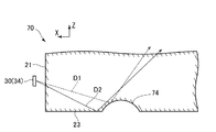
次に、例1として拡散部74の深さDeが上述した規定の範囲外である導光体70と、例2として拡散部24の深さDeが上述した規定の範囲内(50%)である導光体20と、を用いて光が拡散される状態についてそれぞれ説明する。
図7Aは、例1の場合に拡散される状態を示す図である。図7Aに示すように、光源30からの光のうち拡散部74の頂点付近に照射された光D1は拡散部74によって反射され、導光体70の長手方向に向かって進む。また、光源30からの光のうち拡散部74の手前、すなわち光源30側の反射面23に照射された光D2も、そのまま導光体70の長手方向に向かって進む。したがって、光D1および光D2の何れも同様の方向に進む。
Next, the light guide 70 in which the depth De of the diffusing portion 74 is outside the above-described prescribed range as Example 1, and the depth De of the diffusing portion 24 in Example 2 is within the prescribed range (50%) as Example 2. A state where light is diffused using a certain light guide 20 will be described.
FIG. 7A is a diagram illustrating a state of being diffused in the case of Example 1. As shown in FIG. 7A, the light D <b> 1 irradiated near the vertex of the diffusing unit 74 among the light from the light source 30 is reflected by the diffusing unit 74 and travels in the longitudinal direction of the light guide 70. Further, the light D2 emitted from the light source 30 before the diffusing portion 74, that is, the light reflecting surface 23 on the light source 30 side, also travels in the longitudinal direction of the light guide 70 as it is. Therefore, both the light D1 and the light D2 travel in the same direction.

図7Bは、例2の場合に拡散される状態を示す図である。図7Bに示すように、光源30からの光のうち拡散部24の頂点付近に照射された光E1は拡散部24によって反射され、導光体20の長手方向に向かって進む。一方、光源30からの光のうち拡散部24の手前、すなわち光源30側の反射面23に照射された光E2は、拡散部24のうち、反射面23に対して迫り立った傾斜角度の大きな面によって反射されることで、光E1とは異なる方向に拡散される。ここでは、拡散部24によって反射された光は拡散部24のほぼ上方に向かう。   FIG. 7B is a diagram illustrating a state of being diffused in the case of Example 2. As shown in FIG. 7B, the light E <b> 1 irradiated near the apex of the diffusing unit 24 among the light from the light source 30 is reflected by the diffusing unit 24 and travels in the longitudinal direction of the light guide 20. On the other hand, the light E2 emitted from the light source 30 before the diffusing unit 24, that is, the light reflecting surface 23 on the light source 30 side, has a large inclination angle that is close to the reflecting surface 23 in the diffusing unit 24. By being reflected by the surface, it is diffused in a direction different from that of the light E1. Here, the light reflected by the diffusing unit 24 travels substantially upward of the diffusing unit 24.

このように、拡散部24は深さDeが球の直径Diに対して16.5%以上50%以下、更には35%以上50%以下にすることで、拡散部24の深さDeを大きくすることができる。拡散部24の深さDeを大きくするほど、拡散部24には反射面23に対して迫り立った傾斜角度の大きな面が形成される。拡散部24のうち傾斜角度の大きな面は、光源30からの光のうち反射面23によって反射された光をすくい上げるように反射させることから、他の光と異なる方向に光を拡散することができる。   Thus, the diffusion portion 24 has a depth De of 16.5% or more and 50% or less, more preferably 35% or more and 50% or less of the sphere diameter Di, thereby increasing the depth De of the diffusion portion 24. can do. As the depth De of the diffusing portion 24 is increased, the diffusing portion 24 is formed with a surface having a large inclination angle that is close to the reflecting surface 23. The surface having a large inclination angle in the diffusing unit 24 reflects the light reflected by the reflecting surface 23 out of the light from the light source 30 so that the light can be diffused in a direction different from other light. .

<拡散部の幅>
次に、本実施形態の拡散部24は、球状の精度を維持したり、拡散の効率を向上させたりするために、以下のような幅で形成されている。
図1(b)は、それぞれ反射面23に配置された拡散部24の一例を示す図である。
ここでは、図1(b)に示すように、導光体20の反射面23の幅をWrとし、拡散部24の幅をWdとする。幅とは導光体20の長手方向に対して直交する方向かつ反射面23と平行な方向をいうものとする。例えば、上述した一実施例と同様のものとすると、反射面23の幅Wr=0.98mm、拡散部24の幅Wd=0.19mmを有する導光体20を製造することができる。
なお、拡散部24の幅Wdを測定する場合、上述した拡散部24を測定する場合と同様の測定機器、ソフトウェア、および、測定条件とする。
また、拡散部24の幅Wdを測定する場合には、拡散部24の最も深い位置を通過すると共に、反射面23に対して直交かつ幅方向に平行な平面に沿って切断した場合の切断形状を導出する。次に、切断形状上に任意の3点を選択し、選択した3点を通過する仮想円を設定する。仮想円を複数設定し、設定した全ての仮想円ごとに仮想円と、反射面23を延長させた面とが交差する2つの点間を測定し、その平均距離を、拡散部24の幅Wdとする。また、反射面23の幅を測定する場合、第1側面25と反射面23との境界あるいは第2側面26と反射面23との境界に面取りがされている場合には、面取りがされていないと仮定した場合の境界が測定する開始点および終了点である。
<Width of diffusion part>
Next, the diffusion part 24 of the present embodiment is formed with the following width in order to maintain the spherical accuracy and improve the efficiency of diffusion.
FIG. 1B is a diagram illustrating an example of the diffusing unit 24 disposed on the reflecting surface 23.
Here, as shown in FIG. 1B, the width of the reflecting surface 23 of the light guide 20 is Wr, and the width of the diffusion portion 24 is Wd. The width means a direction orthogonal to the longitudinal direction of the light guide 20 and a direction parallel to the reflecting surface 23. For example, if it is the same as that of the above-described embodiment, the light guide 20 having the width Wr = 0.98 mm of the reflecting surface 23 and the width Wd = 0.19 mm of the diffusing portion 24 can be manufactured.
When measuring the width Wd of the diffusing unit 24, the measurement equipment, software, and measurement conditions are the same as those for measuring the diffusing unit 24 described above.
Further, when measuring the width Wd of the diffusing portion 24, the cut shape when passing along the deepest position of the diffusing portion 24 and cutting along a plane orthogonal to the reflecting surface 23 and parallel to the width direction. Is derived. Next, arbitrary three points are selected on the cut shape, and a virtual circle passing through the selected three points is set. A plurality of virtual circles are set, and for every set virtual circle, the distance between two points where the virtual circle intersects with the surface obtained by extending the reflecting surface 23 is measured, and the average distance is calculated as the width Wd of the diffusing unit 24. And Further, when measuring the width of the reflecting surface 23, if the chamfer is chamfered at the boundary between the first side surface 25 and the reflecting surface 23 or the boundary between the second side surface 26 and the reflecting surface 23, the chamfering is not performed. The boundary when assuming that is the start point and the end point to be measured.

本実施形態では、拡散部24の幅Wdは0.1mm以上であることが好ましい。拡散部24の幅Wdを0.1mm以上とすることで、拡散部24を加工したり成形したりするのが容易なためである。特に、金型を用いて導光体20を射出成形で製造する場合に好ましく、より具体的には金型を電極により放電加工で作製する場合に好ましい。
また、本実施形態では、拡散部24の幅Wdは、反射面23の幅Wrに対して50%以下であることが好ましい。ここで、拡散部24の幅Wdを反射面23の幅Wrに対して50%以下に規定するのは、50%よりも大きい場合には反射面23の幅方向に沿って一つの拡散部24のみしか配置できないためである。反射面23の幅方向に沿って少なくとも2つの拡散部24を配置することで、光源30からの光を拡散させる効率を向上させることができる。
In the present embodiment, the width Wd of the diffusing portion 24 is preferably 0.1 mm or more. This is because, by setting the width Wd of the diffusing portion 24 to 0.1 mm or more, it is easy to process or mold the diffusing portion 24. In particular, it is preferable when the light guide 20 is manufactured by injection molding using a mold, and more specifically when the mold is manufactured by electric discharge machining with an electrode.
In the present embodiment, the width Wd of the diffusing portion 24 is preferably 50% or less with respect to the width Wr of the reflecting surface 23. Here, the width Wd of the diffusing portion 24 is regulated to 50% or less with respect to the width Wr of the reflecting surface 23. When the width Wd is larger than 50%, one diffusing portion 24 is formed along the width direction of the reflecting surface 23. This is because it can only be placed. By disposing at least two diffusing portions 24 along the width direction of the reflecting surface 23, the efficiency of diffusing light from the light source 30 can be improved.

更に、拡散部24の幅Wdは、反射面23の幅Wrに対して15%以上30%以下であることが好ましい。拡散部24の幅Wdを反射面23の幅Wrに対して30%以下に規定するのは、反射面23の幅方向に沿って3つ以上の拡散部24を配置できるようにするためである。すなわち、反射面23の幅方向に沿って3つ以上の拡散部24を配置することで、光源30からの光を拡散させる効率をより向上させることができる。一方、拡散部24の幅Wdを反射面23の幅Wrに対して15%以上に規定するのは、反射面23の幅方向に沿って5つ以下の拡散部24を配置するためである。すなわち、反射面23の幅方向に沿って6つ以上の拡散部24を配置するのは、多くの工程が必要になり製造コストが掛かってしまうためである。特に、金型を用いて導光体20を射出成形で製造する場合、金型を電極により放電加工で作製する際には、電極に対して拡散部24に相当する小さな球状を一つずつ加工すると製造コストが上昇してしまう。
なお、拡散部24の曲面と一致する仮想球と、反射面23の面とが交差する形状は円となる。したがって、拡散部24の幅とは、拡散部24の仮想球と反射面23とが交差する円の直径と同一である。
Furthermore, the width Wd of the diffusing portion 24 is preferably 15% or more and 30% or less with respect to the width Wr of the reflecting surface 23. The reason why the width Wd of the diffusing portion 24 is regulated to 30% or less with respect to the width Wr of the reflecting surface 23 is to allow three or more diffusing portions 24 to be arranged along the width direction of the reflecting surface 23. . That is, the efficiency of diffusing light from the light source 30 can be further improved by disposing three or more diffusing portions 24 along the width direction of the reflecting surface 23. On the other hand, the reason why the width Wd of the diffusing portion 24 is defined to be 15% or more with respect to the width Wr of the reflecting surface 23 is to arrange five or less diffusing portions 24 along the width direction of the reflecting surface 23. That is, the reason why the six or more diffusion parts 24 are arranged along the width direction of the reflection surface 23 is that many processes are required and the manufacturing cost is increased. In particular, when the light guide 20 is manufactured by injection molding using a mold, when the mold is manufactured by electric discharge machining with an electrode, small spheres corresponding to the diffusion portions 24 are processed one by one with respect to the electrode. Then, manufacturing cost will rise.
The virtual sphere that coincides with the curved surface of the diffusing unit 24 and the surface of the reflecting surface 23 intersect with each other to form a circle. Accordingly, the width of the diffusing portion 24 is the same as the diameter of the circle where the phantom sphere of the diffusing portion 24 and the reflecting surface 23 intersect.

<拡散部の数>
次に、本実施形態の拡散部24は、拡散の効率を向上させたり、導光体20の製造コストを削減したりするために、以下のような数で形成されている。
本実施形態では、拡散部24の数は幅方向に沿って直線状に2つ以上5つ以下で配置されていることが好ましい。ここで、拡散部24の数を幅方向に沿って直線状に2つ以上に規定するのは、反射面23の幅方向に沿って2つの拡散部24を配置することで、光源30からの光を拡散させる効率を向上させることができるためである。
また、拡散部24の数を幅方向に沿って5つ以下に規定するのは、反射面23の幅方向に沿って6つ以上の拡散部24を配置するのは、多くの加工が必要になり製造コストが掛かってしまうためである。図1(c)には、拡散部24の数を幅方向に沿って直線状に5つにした導光体20を示している。
<Number of diffusion parts>
Next, in order to improve the diffusion efficiency and reduce the manufacturing cost of the light guide 20, the diffusion unit 24 of the present embodiment is formed with the following number.
In this embodiment, it is preferable that the number of the diffusing portions 24 is linearly arranged in the width direction with 2 or more and 5 or less. Here, the number of the diffusing portions 24 is defined to be two or more linearly along the width direction by arranging the two diffusing portions 24 along the width direction of the reflecting surface 23. This is because the efficiency of diffusing light can be improved.
In addition, the number of diffusing parts 24 is defined to be five or less along the width direction. The arrangement of six or more diffusing parts 24 along the width direction of the reflecting surface 23 requires a lot of processing. This is because the manufacturing cost is increased. FIG. 1C shows a light guide 20 in which the number of diffusing portions 24 is five linearly along the width direction.

このように、本実施形態によれば、拡散部24は、反射面23からの深さが球状の直径に対して16.5%以上50%以下である。したがって、拡散部24は光源30から照射された光のうち反射面23により反射された光をすくい上げるように反射させることから、導光体20の出射面22から出射させる光を導光体20の長手方向に拡散させることができる。
また、本実施形態によれば、拡散部24は、幅が0.1mm以上であって反射面23の幅に対して50%以下であることから、拡散部24の形状を容易に加工したり成形したりすることができる。
なお、拡散部24が球状の場合には反射面23の面に表れる拡散部24の形状は円となる。ここで、拡散部24は、反射面23に表れる拡散部24の円の曲率が1.5〜20になるような球状であることが好ましい。曲率1.5とは円の直径が1.33mmであり、曲率20とは円の直径が0.1mmである。このような範囲に規定することで、光源30からの光を幅方向に拡散させる効率を向上させることができる。なお、円の直径の測定は、拡散部24の幅Wdを測定する場合と同様の測定方法を適用することができる。すなわち、拡散部24が球状の場合には、拡散部24の幅Wdが、反射面23に表れる拡散部24の円の直径となる。なお、円全体あるいは一部が歪んでいたとしても、製造誤差の範囲は円の概念に含まれる。
Thus, according to this embodiment, the diffusion part 24 has a depth from the reflecting surface 23 of 16.5% or more and 50% or less with respect to the spherical diameter. Therefore, the diffusing unit 24 reflects the light reflected by the reflecting surface 23 out of the light emitted from the light source 30 so as to scoop up the light emitted from the emitting surface 22 of the light guide 20. It can be diffused in the longitudinal direction.
In addition, according to the present embodiment, since the diffusion portion 24 has a width of 0.1 mm or more and 50% or less with respect to the width of the reflection surface 23, the shape of the diffusion portion 24 can be easily processed. Or can be molded.
When the diffusing portion 24 is spherical, the shape of the diffusing portion 24 that appears on the surface of the reflecting surface 23 is a circle. Here, the diffusing portion 24 is preferably spherical so that the curvature of the circle of the diffusing portion 24 appearing on the reflecting surface 23 is 1.5-20. A curvature of 1.5 means a circle diameter of 1.33 mm, and a curvature of 20 means a circle diameter of 0.1 mm. By defining in such a range, the efficiency of diffusing light from the light source 30 in the width direction can be improved. In addition, the measurement method similar to the case of measuring the width Wd of the diffusion part 24 can be applied to the measurement of the diameter of the circle. That is, when the diffusing portion 24 is spherical, the width Wd of the diffusing portion 24 is the diameter of the circle of the diffusing portion 24 that appears on the reflecting surface 23. Even if the entire circle or a part of the circle is distorted, the range of manufacturing error is included in the concept of circle.

(第2の実施形態)
図8Aは、第2の実施形態の導光体80の拡散部24を示す拡大断面図である。なお、第1の実施形態と同様の構成には同一符号を付してその説明を省略する。
本実施形態の導光体80は、反射面23と拡散部24との境界に亘って傾斜部81を有する。このように傾斜部81を有することで、光源30からの光のうち反射面23とほぼ平行に照射された光を、傾斜部81および拡散部24ですくい上げるように反射させることができる。すなわち、図8Aの一点鎖線を拡大した図に示すように、光源30からの光のうち拡散部24の手前、すなわち光源30側の反射面23に照射された光Fは、傾斜部81により反射された後、拡散部24により更に反射される。したがって、光源30からの光のうち反射面23によって反射された光をすくい上げるように反射させることから、他の光と異なる方向に光を拡散することができる。
このように、本実施形態の導光体80は、拡散部24が反射面23に対して凹んだ形状であって、反射面23と拡散部24との境界に傾斜部81を有することを特徴とするものである。
なお、本実施形態では、傾斜部81が直線状である場合について説明したが、この場合に限られず、曲線状であってもよい。また、拡散部24の形状は球状に限定されない。
(Second Embodiment)
FIG. 8A is an enlarged cross-sectional view showing the diffusion portion 24 of the light guide 80 according to the second embodiment. In addition, the same code | symbol is attached | subjected to the structure similar to 1st Embodiment, and the description is abbreviate | omitted.
The light guide 80 of the present embodiment has an inclined portion 81 across the boundary between the reflecting surface 23 and the diffusing portion 24. By having the inclined portion 81 in this way, light irradiated from the light source 30 substantially parallel to the reflecting surface 23 can be reflected so as to be picked up by the inclined portion 81 and the diffusing portion 24. That is, as shown in the enlarged view of the alternate long and short dash line in FIG. 8A, the light F emitted from the light source 30 before the diffusing unit 24, that is, the reflecting surface 23 on the light source 30 side is reflected by the inclined unit 81. Then, the light is further reflected by the diffusing unit 24. Therefore, since the light reflected by the reflecting surface 23 out of the light from the light source 30 is reflected so as to be scooped up, the light can be diffused in a direction different from other light.
Thus, the light guide 80 of the present embodiment has a shape in which the diffusing portion 24 is recessed with respect to the reflecting surface 23, and has an inclined portion 81 at the boundary between the reflecting surface 23 and the diffusing portion 24. It is what.
In addition, although this embodiment demonstrated the case where the inclination part 81 was linear, it is not restricted to this case, A curved shape may be sufficient. Further, the shape of the diffusion portion 24 is not limited to a spherical shape.

次に、傾斜部が曲線状である場合について説明する。
図8Bは、傾斜部82が曲線状である拡散部24の拡大断面図である。
傾斜部82は、拡散部24が反射面23において角が取られた形状である。ここで、拡散部24の形状を幾何学的に円の周であると近似すると、反射面23側では近似した円の開口よりも広い開口が得られる。図8Bの一点鎖線を拡大した図には、近似した円の周を破線で示している。
Next, a case where the inclined portion is curved will be described.
FIG. 8B is an enlarged cross-sectional view of the diffusing portion 24 in which the inclined portion 82 is curved.
The inclined portion 82 has a shape in which the diffusing portion 24 is rounded at the reflecting surface 23. Here, when the shape of the diffusing portion 24 is approximated geometrically around a circle, an opening wider than the approximate circular opening is obtained on the reflecting surface 23 side. In the enlarged view of the alternate long and short dash line in FIG. 8B, the circumference of the approximate circle is indicated by a broken line.

上述したような傾斜部81、82の形状は、面取りによって得ることができる。あるいは、傾斜部81、82の形状は、金型が有する傾斜部の形状が転写されることで得ることができる。なお、金型が有する傾斜部の形状は、放電加工に用いる電極の形状によって得られる。放電加工された電極は、導光体80の凹部に対応する凸部の細かなデコボコを除去するために、凸部を含む成形用の面が研磨される。
上述したような傾斜部81、82の形状は、導光体80を金型により成形する際、金型から導光体を容易に外すことができるので、好ましい形状である。特に、本実施形態のように、ドット状の微細な凹部を複数有する細かい導光体80を金型によって成形する際に好ましい。
また、傾斜部81、82を観察する場合、上述した拡散部24を測定する場合と同様の測定機器、ソフトウェア、および、測定条件とすることで、観察可能である。
The shape of the inclined portions 81 and 82 as described above can be obtained by chamfering. Alternatively, the shape of the inclined portions 81 and 82 can be obtained by transferring the shape of the inclined portion of the mold. Note that the shape of the inclined portion of the mold is obtained by the shape of the electrode used for electric discharge machining. In the electrode subjected to electric discharge machining, the molding surface including the convex portion is polished in order to remove the fine unevenness of the convex portion corresponding to the concave portion of the light guide 80.
The shape of the inclined portions 81 and 82 as described above is a preferable shape because the light guide can be easily removed from the mold when the light guide 80 is formed by the mold. In particular, as in the present embodiment, it is preferable when a fine light guide 80 having a plurality of fine dot-like concave portions is formed by a mold.
Moreover, when observing the inclination parts 81 and 82, it is observable by setting it as the measurement apparatus, software, and measurement conditions similar to the case where the spreading | diffusion part 24 mentioned above is measured.

上述したように第1および第2の実施形態では、拡散部24の形状が球状である場合について説明したが、拡散部24の形状は湾曲状形状であればよく、例えば楕円状であってもよい。
導光体20の反射面23に設けられる凹部である拡散部24は、出射面22に向かって凸の湾曲状であるだけでなく、配置されている光源30に向かって凸の湾曲状であることが光をより拡散させやすく、導光体20の幅方向に光を均一化させやすいために好ましい。出射面22に向かって凸に湾曲している形状であること、および、光源30に向かって凸に湾曲している形状であることの両方を満たす形状として、球状あるいは楕円状といった湾曲状形状が好ましい。
As described above, in the first and second embodiments, the case where the shape of the diffusing portion 24 is spherical has been described. However, the shape of the diffusing portion 24 may be a curved shape, for example, an elliptical shape. Good.
The diffusing portion 24, which is a recess provided in the reflecting surface 23 of the light guide 20, is not only convexly curved toward the emission surface 22, but also convex toward the light source 30 disposed. This is preferable because light is more easily diffused and light is easily uniformed in the width direction of the light guide 20. A curved shape such as a spherical shape or an oval shape is used as a shape satisfying both the shape curved convexly toward the emission surface 22 and the shape curved convexly toward the light source 30. preferable.

本発明に係る拡散部は、本実施形態や第2の実施形態で説明した球状の拡散部24以外に、楕円状であってもよい。拡散部が球状であったり楕円状であったりしてもよいということは、拡散部は反射面23から凹んだ湾曲状形状ということである。また、本発明に係る拡散部は、反射面において、光源30に向かって凸に例えば円形状や楕円形状のように湾曲している。すなわち、本発明に係る拡散部は、反射面23からの深さ方向(図1のZ方向)においても反射面23の幅方向(図1のY方向)においても湾曲している。
そして、拡散部の深さ方向の大きさや幅方向の大きさは、レーザ顕微鏡で観察した最も深い場所において設定した仮想円から求めることができる。その場合の拡散部の深さの数値範囲は、上述の数値範囲と同一、すなわち仮想円の16.5%以上50%以下であり、拡散部の幅も0.1mm以上であって反射面23の幅に対して50%以下である。
The diffuser according to the present invention may be elliptical in addition to the spherical diffuser 24 described in the present embodiment or the second embodiment. That the diffusing portion may be spherical or elliptical means that the diffusing portion has a curved shape that is recessed from the reflecting surface 23. Further, the diffusing portion according to the present invention is curved in a convex manner toward the light source 30 such as a circular shape or an elliptical shape on the reflecting surface. That is, the diffusing portion according to the present invention is curved both in the depth direction from the reflecting surface 23 (Z direction in FIG. 1) and in the width direction of the reflecting surface 23 (Y direction in FIG. 1).
Then, the size in the depth direction and the size in the width direction of the diffusion part can be obtained from a virtual circle set at the deepest place observed with a laser microscope. In this case, the numerical range of the depth of the diffusing portion is the same as the above-described numerical range, that is, 16.5% to 50% of the imaginary circle, the width of the diffusing portion is 0.1 mm or more, and the reflecting surface 23 It is 50% or less with respect to the width | variety.

(第3の実施形態)
次に、上述したイメージセンサユニット10を画像読取装置としてのフラットベッド方式のスキャナ130に適用した構成について図9を参照して説明する。
図9は、フラットベッド方式のスキャナ130の構成の一例を示す斜視図である。
スキャナ130は、筺体131と、被照明体載置部としてのプラテンガラス132と、イメージセンサユニット10と、イメージセンサユニット10を駆動する駆動機構と、回路基板133と、プラテンカバー134とを有する。プラテンガラス132は、ガラスなどの透明板からなり、筺体131の上面に取り付けられる。プラテンカバー134は、プラテンガラス132に載置された原稿Pを覆うように、筺体131に対してヒンジ機構などを介して開閉可能に取り付けられる。イメージセンサユニット10と、イメージセンサユニット10を駆動するための駆動機構と、回路基板133とは、筺体131内に収容される。
(Third embodiment)
Next, a configuration in which the above-described image sensor unit 10 is applied to a flatbed scanner 130 as an image reading apparatus will be described with reference to FIG.
FIG. 9 is a perspective view illustrating an example of the configuration of the flatbed scanner 130.
The scanner 130 includes a housing 131, a platen glass 132 serving as an illuminated body placement unit, the image sensor unit 10, a drive mechanism that drives the image sensor unit 10, a circuit board 133, and a platen cover 134. The platen glass 132 is made of a transparent plate such as glass, and is attached to the upper surface of the casing 131. The platen cover 134 is attached to the casing 131 so as to be openable and closable via a hinge mechanism or the like so as to cover the document P placed on the platen glass 132. The image sensor unit 10, a drive mechanism for driving the image sensor unit 10, and the circuit board 133 are accommodated in the housing 131.

駆動機構は、保持部材135と、ガイドシャフト136と、駆動モータ137と、ワイヤ138とを含む。保持部材135は、イメージセンサユニット10を囲むように保持する。ガイドシャフト136は、保持部材135をプラテンガラス132に沿って読取方向(副走査方向)に移動可能にガイドする。駆動モータ137と保持部材135とはワイヤ138を介して連結されており、駆動モータ137の駆動力によってイメージセンサユニット10を保持する保持部材135を副走査方向に移動させる。そして、イメージセンサユニット10は、駆動モータ137の駆動力によって副走査方向に移動しながら、プラテンガラス132に載置された原稿Pを読取る。このように、イメージセンサユニット10と原稿Pとを相対的に移動させながら、原稿Pを読取る。   The drive mechanism includes a holding member 135, a guide shaft 136, a drive motor 137, and a wire 138. The holding member 135 holds the image sensor unit 10 so as to surround it. The guide shaft 136 guides the holding member 135 so as to be movable along the platen glass 132 in the reading direction (sub-scanning direction). The drive motor 137 and the holding member 135 are connected via a wire 138, and the holding member 135 that holds the image sensor unit 10 is moved in the sub-scanning direction by the driving force of the drive motor 137. The image sensor unit 10 reads the document P placed on the platen glass 132 while moving in the sub-scanning direction by the driving force of the driving motor 137. In this way, the document P is read while relatively moving the image sensor unit 10 and the document P.

回路基板133には、イメージセンサユニット10が読取った画像に所定の画像処理を施す画像処理回路や、イメージセンサユニット10を含むスキャナ130の各部を制御する制御回路や、スキャナ130の各部に電力を供給する電源回路などが構築される。   The circuit board 133 includes an image processing circuit that performs predetermined image processing on an image read by the image sensor unit 10, a control circuit that controls each part of the scanner 130 including the image sensor unit 10, and power to each part of the scanner 130. A power supply circuit to be supplied is constructed.

(第4の実施形態)
次に、上述したイメージセンサユニット10を画像読取装置としてのシートフィード方式のスキャナ140に適用した構成について図10を参照して説明する。
図10は、シートフィード方式のスキャナ140の構成の一例を示す断面図である。
スキャナ140は、筺体141と、イメージセンサユニット10と、搬送ローラ142と、回路基板143とを有する。搬送ローラ142は、図示しない駆動機構によって回転し、原稿Pを挟んで搬送する。回路基板143には、イメージセンサユニット10を含むスキャナ140の各部を制御する制御回路や、スキャナ140の各部に電力を供給する電源回路などが構築される。
(Fourth embodiment)
Next, a configuration in which the above-described image sensor unit 10 is applied to a sheet feed type scanner 140 as an image reading apparatus will be described with reference to FIG.
FIG. 10 is a cross-sectional view illustrating an example of the configuration of the sheet feed type scanner 140.
The scanner 140 includes a housing 141, the image sensor unit 10, a conveyance roller 142, and a circuit board 143. The conveyance roller 142 is rotated by a driving mechanism (not shown) and conveys the document P with the document P interposed therebetween. On the circuit board 143, a control circuit that controls each part of the scanner 140 including the image sensor unit 10, a power supply circuit that supplies power to each part of the scanner 140, and the like are constructed.

そして、スキャナ140は、搬送ローラ142によって原稿Pを読取り方向(副走査方向)に搬送しつつ、イメージセンサユニット10により原稿Pを読取る。すなわち、イメージセンサユニット10と原稿Pとを相対的に移動させながら、原稿Pを読取る。なお、図10では、原稿Pの片面を読取るスキャナ140の例を示すが、2つのイメージセンサユニット10が原稿Pの搬送経路を挟んで対向するように設けられ、原稿Pの両面を読取る構成であってもよい。   The scanner 140 reads the document P by the image sensor unit 10 while transporting the document P in the reading direction (sub-scanning direction) by the transport roller 142. That is, the document P is read while relatively moving the image sensor unit 10 and the document P. FIG. 10 shows an example of the scanner 140 that reads one side of the document P, but two image sensor units 10 are provided so as to face each other with the conveyance path of the document P interposed therebetween, and read both sides of the document P. There may be.

以上、本発明を上述した実施形態により説明したが、本発明は上述した実施形態にのみ限定されるものではなく、本発明の範囲内で変更が可能である。
上述した実施形態では、拡散部24は規則的なパターンにしたがって反射面23に配置する場合について説明したが、この場合に限られず不規則に配置してもよい。この場合であって、反射面23では入射面21側から他端面27側に向かうにしたがって徐々に反射面23に対する拡散部24の密度が増大させることで、導光体20の長手方向における何れの位置からでも所望する光量を出射面22から出射させることができる。
As mentioned above, although this invention was demonstrated by embodiment mentioned above, this invention is not limited only to embodiment mentioned above, It can change within the scope of the present invention.
In the embodiment described above, the case where the diffusing unit 24 is arranged on the reflecting surface 23 according to a regular pattern has been described. However, the present invention is not limited to this case and may be arranged irregularly. In this case, in the reflecting surface 23, the density of the diffusing portion 24 with respect to the reflecting surface 23 is gradually increased from the incident surface 21 side toward the other end surface 27 side. A desired amount of light can be emitted from the emission surface 22 even from the position.

上述した実施形態では、導光体20が第1側面25および第2側面26などの反射面を有する場合について説明したが、この場合に限られず、その他の反射面を有していてもよい。
上述した実施形態では、導光体20が入射面21から他端面27まで長手方向に連続する直線状である場合について説明したが、この場合に限られず、曲部を有する導光体を用いてもよい。具体的には、導光体として、主走査方向に長い棒状に形成された光出射部と、光出射部の一方側の端部から曲がって形成された曲部とを有する導光体を採用することができる。この場合、曲部の端面を光源30から光が入射される入射面とすることができ、光源30を回路基板40の表面に実装する表面実装型のLEDパッケージとすることができる。
上述した実施形態では、導光体20を大量生産に適した射出成形で製造する場合について説明したが、この場合に限られず、小量生産に適した切削加工により製造してもよい。
なお、移動手段としての移動部は、イメージセンサユニット10と原稿Pとの少なくとも何れかを相対的に移動させることができる。
In the embodiment described above, the case where the light guide 20 has the reflecting surfaces such as the first side surface 25 and the second side surface 26 has been described. However, the present invention is not limited to this case, and may have other reflecting surfaces.
In the above-described embodiment, the case where the light guide 20 has a linear shape continuous in the longitudinal direction from the incident surface 21 to the other end surface 27 has been described. However, the present invention is not limited to this, and a light guide having a curved portion is used. Also good. Specifically, as the light guide, a light guide having a light emitting portion formed in a rod shape long in the main scanning direction and a curved portion formed by bending from one end of the light emitting portion is adopted. can do. In this case, the end surface of the curved portion can be an incident surface on which light is incident from the light source 30, and a surface mount type LED package in which the light source 30 is mounted on the surface of the circuit board 40 can be obtained.
In the above-described embodiment, the case where the light guide 20 is manufactured by injection molding suitable for mass production has been described. However, the present invention is not limited to this, and may be manufactured by cutting suitable for small-volume production.
Note that the moving unit as the moving unit can relatively move at least one of the image sensor unit 10 and the document P.

10:イメージセンサユニット 11:フレーム 12:導光体収容部 13:保持部 20:導光体 21:入射面 22:出射面 23:反射面 24:拡散部 27:他端面 81,82:傾斜部 30:光源 40:回路基板 50:イメージセンサ 60:集光体 100:MFP(画像読取装置、画像形成装置) 101:シート(記録媒体) 102:画像読取部 108:イメージセンサユニット駆動モータ 113:画像形成部   DESCRIPTION OF SYMBOLS 10: Image sensor unit 11: Frame 12: Light guide housing | casing part 13: Holding part 20: Light guide 21: Incident surface 22: Outgoing surface 23: Reflecting surface 24: Diffusing part 27: Other end surface 81,82: Inclined part 30: Light source 40: Circuit board 50: Image sensor 60: Light collector 100: MFP (image reading device, image forming device) 101: Sheet (recording medium) 102: Image reading unit 108: Image sensor unit drive motor 113: Image Forming part

Claims (8)

光源と長尺状の導光体とを有する照明装置であって、
前記導光体は、前記光源からの光を出射する出射面と、前記光を前記出射面へ反射する反射面とを有し、
前記反射面は、前記光を拡散させる拡散部を複数有し、
前記拡散部は、
前記反射面から凹んだ球の一部の形状であって、
前記反射面からの深さが前記球の直径に対して16.5%以上50%以下であり、
前記反射面と平行な方向かつ前記反射面の長手方向に対して直交する方向である幅が0.1mm以上であって前記反射面の幅に対して50%以下であることを特徴とする照明装置。
An illumination device having a light source and a long light guide,
The light guide has an exit surface that emits light from the light source, and a reflective surface that reflects the light to the exit surface,
The reflective surface has a plurality of diffusion parts that diffuse the light,
The diffusion part is
A shape of a part of a sphere recessed from the reflecting surface,
The depth from the reflecting surface is 16.5% or more and 50% or less with respect to the diameter of the sphere,
A width which is a direction parallel to the reflecting surface and perpendicular to the longitudinal direction of the reflecting surface is 0.1 mm or more and 50% or less with respect to the width of the reflecting surface. apparatus.
前記拡散部は、
前記反射面からの深さが前記球の直径に対して35%以上50%以下であることを特徴とする請求項1に記載の照明装置。
The diffusion part is
The lighting device according to claim 1, wherein a depth from the reflecting surface is 35% or more and 50% or less with respect to a diameter of the sphere.
前記拡散部は、
幅が前記反射面の幅に対して15%以上30%以下であることを特徴とする請求項1または2に記載の照明装置。
The diffusion part is
The lighting device according to claim 1 or 2, wherein the width is 15% or more and 30% or less with respect to the width of the reflecting surface.
前記拡散部は、
前記反射面の幅方向に沿って直線状に2つ以上5つ以下で配置されていることを特徴とする請求項1ないし3の何れか1項に記載の照明装置。
The diffusion part is
4. The lighting device according to claim 1, wherein two or more and five or less are arranged linearly along the width direction of the reflecting surface. 5.
前記導光体は、
前記反射面と前記拡散部との境界に傾斜部を有することを特徴とする請求項1ないし4の何れか1項に記載の照明装置。
The light guide is
5. The lighting device according to claim 1, further comprising an inclined portion at a boundary between the reflecting surface and the diffusing portion.
被照明体に照射した光を読取るセンサユニットであって、
請求項1ないし5の何れか1項に記載の照明装置と、
前記照明装置により前記被照明体を照射して反射した光を結像する集光体と、
前記集光体によって結像された光を電気信号に変換するセンサと、を備えることを特徴とするセンサユニット。
A sensor unit for reading light irradiated to an illuminated object,
The lighting device according to any one of claims 1 to 5,
A condenser for imaging the light reflected by illuminating the object to be illuminated by the illumination device;
A sensor unit that converts light imaged by the light collector into an electrical signal.
請求項6に記載のセンサユニットと、
前記センサユニットと前記被照明体との少なくとも何れかを相対的に移動させる移動手段と、を有することを特徴とする読取装置。
The sensor unit according to claim 6,
A reading device comprising: moving means for relatively moving at least one of the sensor unit and the object to be illuminated.
請求項6に記載のセンサユニットと、
前記センサユニットと前記被照明体との少なくとも何れかを相対的に移動させる移動手段と、
前記センサユニットにより読取られた画像を記録媒体に形成する画像形成手段と、を有することを特徴とする画像形成装置。
The sensor unit according to claim 6,
Moving means for relatively moving at least one of the sensor unit and the object to be illuminated;
An image forming apparatus comprising: an image forming unit that forms an image read by the sensor unit on a recording medium.
JP2017073656A 2016-04-08 2017-04-03 Lighting device, sensor unit, reader and image forming device Active JP6768586B2 (en)

Priority Applications (1)

Application Number Priority Date Filing Date Title
US15/481,740 US10136019B2 (en) 2016-04-08 2017-04-07 Illumination apparatus, sensor unit, and reading apparatus

Applications Claiming Priority (2)

Application Number Priority Date Filing Date Title
JP2016078130 2016-04-08

Publications (3)

Publication Number Publication Date
JP2017192126A true JP2017192126A (en) 2017-10-19
JP2017192126A5 JP2017192126A5 (en) 2020-04-09
JP6768586B2 JP6768586B2 (en) 2020-10-14

Family

ID=60084945

Family Applications (1)

Application Number Title Priority Date Filing Date
JP2017073656A Active JP6768586B2 (en) 2016-04-08 2017-04-03 Lighting device, sensor unit, reader and image forming device

Country Status (1)

Country Link
JP (1) JP6768586B2 (en)

Cited By (1)

* Cited by examiner, † Cited by third party
Publication number Priority date Publication date Assignee Title
WO2023085285A1 (en) * 2021-11-12 2023-05-19 株式会社ジャパンディスプレイ Detection device

Citations (5)

* Cited by examiner, † Cited by third party
Publication number Priority date Publication date Assignee Title
WO2006120932A1 (en) * 2005-05-12 2006-11-16 Nippon Sheet Glass Company, Limited Light guide and image reader
JP2006319591A (en) * 2005-05-12 2006-11-24 Nippon Sheet Glass Co Ltd Line lighting system and image scanner
JP2011087290A (en) * 2009-09-18 2011-04-28 Canon Components Inc Linearly-aligned illuminating device and image reader using the same
JP2013157841A (en) * 2012-01-31 2013-08-15 Kyocera Document Solutions Inc Light guide, illuminating device, and image reading apparatus and image forming apparatus including the same
JP2014235881A (en) * 2013-05-31 2014-12-15 京セラドキュメントソリューションズ株式会社 Transparent material and lighting system

Patent Citations (5)

* Cited by examiner, † Cited by third party
Publication number Priority date Publication date Assignee Title
WO2006120932A1 (en) * 2005-05-12 2006-11-16 Nippon Sheet Glass Company, Limited Light guide and image reader
JP2006319591A (en) * 2005-05-12 2006-11-24 Nippon Sheet Glass Co Ltd Line lighting system and image scanner
JP2011087290A (en) * 2009-09-18 2011-04-28 Canon Components Inc Linearly-aligned illuminating device and image reader using the same
JP2013157841A (en) * 2012-01-31 2013-08-15 Kyocera Document Solutions Inc Light guide, illuminating device, and image reading apparatus and image forming apparatus including the same
JP2014235881A (en) * 2013-05-31 2014-12-15 京セラドキュメントソリューションズ株式会社 Transparent material and lighting system

Cited By (1)

* Cited by examiner, † Cited by third party
Publication number Priority date Publication date Assignee Title
WO2023085285A1 (en) * 2021-11-12 2023-05-19 株式会社ジャパンディスプレイ Detection device

Also Published As

Publication number Publication date
JP6768586B2 (en) 2020-10-14

Similar Documents

Publication Publication Date Title
JP5873907B2 (en) Illumination apparatus, image sensor unit, image reading apparatus, and image forming apparatus
JP5933492B2 (en) Illumination apparatus, image sensor unit, image reading apparatus, and image forming apparatus
JP5384707B2 (en) Image sensor unit and image reading apparatus using the same
JP5815782B2 (en) Image sensor unit, image reading apparatus, and image forming apparatus
JP2016001839A (en) Image sensor unit, image reading device, and image forming apparatus
CN103363351A (en) Illumination apparatus, image sensor unit, image reading apparatus, and image forming apparatus
JP5907935B2 (en) Illumination apparatus, image sensor unit, image reading apparatus, and image forming apparatus
JP6768586B2 (en) Lighting device, sensor unit, reader and image forming device
JP7133681B2 (en) Lighting device, sensor unit, reading device and image forming device
US20140376061A1 (en) Image sensor unit, image reading apparatus, and image forming apparatus
US10091382B2 (en) Illumination apparatus and sensor unit
US10136019B2 (en) Illumination apparatus, sensor unit, and reading apparatus
JP6087069B2 (en) Document scanner
JP2015195152A (en) Illuminating device, image sensor unit, image reading device, and image forming device
JP5251619B2 (en) Image sensor
JPWO2015093112A1 (en) Image sensor unit and manufacturing method thereof, paper sheet identification device, image reading device, and image forming device
JP2017175289A (en) Illumination device, image sensor unit, image reading device, and image forming apparatus
JP6071953B2 (en) Illumination apparatus, image sensor unit, image reading apparatus, and image forming apparatus
US10323825B2 (en) Light guide, illumination device, sensor unit, reading apparatus, image forming apparatus, and paper sheet distinguishing apparatus
JP5813253B2 (en) Illumination device, image sensor unit, paper sheet identification device, image reading device, and image forming device
JP6630618B2 (en) Image sensor unit, paper sheet identification device, image reading device, image forming device
JP2016152565A (en) Image sensor unit, paper sheet identification device, image reading device, and image forming apparatus
JP2018174524A (en) Sensor unit, reading device, and image forming apparatus
JP2018026622A (en) Image sensor unit, paper sheet identification apparatus, image reading device
JP2019029852A (en) Illumination device, sensor unit, reading device, paper sheet reading device, and image forming apparatus

Legal Events

Date Code Title Description
A521 Request for written amendment filed

Free format text: JAPANESE INTERMEDIATE CODE: A523

Effective date: 20200228

A621 Written request for application examination

Free format text: JAPANESE INTERMEDIATE CODE: A621

Effective date: 20200228

A871 Explanation of circumstances concerning accelerated examination

Free format text: JAPANESE INTERMEDIATE CODE: A871

Effective date: 20200228

A975 Report on accelerated examination

Free format text: JAPANESE INTERMEDIATE CODE: A971005

Effective date: 20200407

A131 Notification of reasons for refusal

Free format text: JAPANESE INTERMEDIATE CODE: A131

Effective date: 20200519

A521 Request for written amendment filed

Free format text: JAPANESE INTERMEDIATE CODE: A523

Effective date: 20200720

TRDD Decision of grant or rejection written
A01 Written decision to grant a patent or to grant a registration (utility model)

Free format text: JAPANESE INTERMEDIATE CODE: A01

Effective date: 20200825

A61 First payment of annual fees (during grant procedure)

Free format text: JAPANESE INTERMEDIATE CODE: A61

Effective date: 20200923

R150 Certificate of patent or registration of utility model

Ref document number: 6768586

Country of ref document: JP

Free format text: JAPANESE INTERMEDIATE CODE: R150

R250 Receipt of annual fees

Free format text: JAPANESE INTERMEDIATE CODE: R250