JP5872790B2 - Semiconductor laser device - Google Patents
Semiconductor laser device Download PDFInfo
- Publication number
- JP5872790B2 JP5872790B2 JP2011100480A JP2011100480A JP5872790B2 JP 5872790 B2 JP5872790 B2 JP 5872790B2 JP 2011100480 A JP2011100480 A JP 2011100480A JP 2011100480 A JP2011100480 A JP 2011100480A JP 5872790 B2 JP5872790 B2 JP 5872790B2
- Authority
- JP
- Japan
- Prior art keywords
- type
- passivation film
- cladding layer
- ridge portion
- film
- Prior art date
- Legal status (The legal status is an assumption and is not a legal conclusion. Google has not performed a legal analysis and makes no representation as to the accuracy of the status listed.)
- Active
Links
- 239000004065 semiconductor Substances 0.000 title claims description 48
- 238000002161 passivation Methods 0.000 claims description 76
- 238000005253 cladding Methods 0.000 claims description 46
- 239000000758 substrate Substances 0.000 claims description 18
- 238000005530 etching Methods 0.000 claims description 5
- 239000011810 insulating material Substances 0.000 claims description 4
- 239000010408 film Substances 0.000 description 108
- 239000010410 layer Substances 0.000 description 53
- 238000000034 method Methods 0.000 description 19
- VYPSYNLAJGMNEJ-UHFFFAOYSA-N Silicium dioxide Chemical compound O=[Si]=O VYPSYNLAJGMNEJ-UHFFFAOYSA-N 0.000 description 14
- 229920002120 photoresistant polymer Polymers 0.000 description 14
- 229910052814 silicon oxide Inorganic materials 0.000 description 14
- 238000004519 manufacturing process Methods 0.000 description 13
- 230000017525 heat dissipation Effects 0.000 description 8
- 238000001312 dry etching Methods 0.000 description 5
- KRHYYFGTRYWZRS-UHFFFAOYSA-N Fluorane Chemical compound F KRHYYFGTRYWZRS-UHFFFAOYSA-N 0.000 description 3
- 229910052581 Si3N4 Inorganic materials 0.000 description 3
- 238000005229 chemical vapour deposition Methods 0.000 description 3
- 229910052751 metal Inorganic materials 0.000 description 3
- 239000002184 metal Substances 0.000 description 3
- HQVNEWCFYHHQES-UHFFFAOYSA-N silicon nitride Chemical compound N12[Si]34N5[Si]62N3[Si]51N64 HQVNEWCFYHHQES-UHFFFAOYSA-N 0.000 description 3
- 238000001039 wet etching Methods 0.000 description 3
- 229910001218 Gallium arsenide Inorganic materials 0.000 description 2
- JMASRVWKEDWRBT-UHFFFAOYSA-N Gallium nitride Chemical compound [Ga]#N JMASRVWKEDWRBT-UHFFFAOYSA-N 0.000 description 2
- 230000010355 oscillation Effects 0.000 description 2
- 229920001721 polyimide Polymers 0.000 description 2
- 239000009719 polyimide resin Substances 0.000 description 2
- 238000009751 slip forming Methods 0.000 description 2
- 239000010409 thin film Substances 0.000 description 2
- 229910002601 GaN Inorganic materials 0.000 description 1
- XUIMIQQOPSSXEZ-UHFFFAOYSA-N Silicon Chemical compound [Si] XUIMIQQOPSSXEZ-UHFFFAOYSA-N 0.000 description 1
- 238000004380 ashing Methods 0.000 description 1
- 230000004888 barrier function Effects 0.000 description 1
- 239000004020 conductor Substances 0.000 description 1
- PMHQVHHXPFUNSP-UHFFFAOYSA-M copper(1+);methylsulfanylmethane;bromide Chemical compound Br[Cu].CSC PMHQVHHXPFUNSP-UHFFFAOYSA-M 0.000 description 1
- 238000000151 deposition Methods 0.000 description 1
- 230000006866 deterioration Effects 0.000 description 1
- 230000000694 effects Effects 0.000 description 1
- 238000007429 general method Methods 0.000 description 1
- 238000010030 laminating Methods 0.000 description 1
- 239000000463 material Substances 0.000 description 1
- 239000012528 membrane Substances 0.000 description 1
- 238000012986 modification Methods 0.000 description 1
- 230000004048 modification Effects 0.000 description 1
- QPJSUIGXIBEQAC-UHFFFAOYSA-N n-(2,4-dichloro-5-propan-2-yloxyphenyl)acetamide Chemical compound CC(C)OC1=CC(NC(C)=O)=C(Cl)C=C1Cl QPJSUIGXIBEQAC-UHFFFAOYSA-N 0.000 description 1
- 230000003287 optical effect Effects 0.000 description 1
- 230000003647 oxidation Effects 0.000 description 1
- 238000007254 oxidation reaction Methods 0.000 description 1
- RVTZCBVAJQQJTK-UHFFFAOYSA-N oxygen(2-);zirconium(4+) Chemical compound [O-2].[O-2].[Zr+4] RVTZCBVAJQQJTK-UHFFFAOYSA-N 0.000 description 1
- 238000000206 photolithography Methods 0.000 description 1
- 230000003252 repetitive effect Effects 0.000 description 1
- 238000004904 shortening Methods 0.000 description 1
- 229910052710 silicon Inorganic materials 0.000 description 1
- 239000010703 silicon Substances 0.000 description 1
- 239000002356 single layer Substances 0.000 description 1
- 238000004528 spin coating Methods 0.000 description 1
- 238000001771 vacuum deposition Methods 0.000 description 1
- 238000007740 vapor deposition Methods 0.000 description 1
- 229910001928 zirconium oxide Inorganic materials 0.000 description 1
Images


Description
本発明は、半導体レーザ装置に関し、特に、半導体レーザ装置の高温・高出力特性の改善に適用して有効な技術に関するものである。 The present invention relates to a semiconductor laser device, and more particularly to a technique effective when applied to improvement of high temperature and high output characteristics of a semiconductor laser device.
特許文献1(特開2009−212521号公報、実施形態2、図5B)は、リッジ導波路を有する窒化ガリウム系半導体レーザにおいて、良好な光閉じ込めと良好な放熱特性とを両立させるために、リッジ部の両側壁およびリッジ部の両側の平坦部(エッチングされた領域)を熱伝導率の高い第1の絶縁膜(例えば窒化アルミニウム)で覆うと共に、リッジ部の側壁の一部(下部)を屈折率の低い第2の絶縁膜(例えば酸化シリコン膜)で覆う技術を開示している。
Patent Document 1 (Japanese Unexamined Patent Application Publication No. 2009-212521,
特許文献2(特開2009−295761号公報)は、リッジストライプの出射端面の近傍において、リッジ部の側壁および上面と、リッジ部の側壁近傍のp型クラッド層上面とをGaN基板との屈折率差が大きい第1誘電体膜(例えば酸化シリコン膜)で覆うと共に、リッジ部上面以外の第1誘電体膜上に第2誘電体膜(例えば酸化ジルコニウム)を積層することにより、低アスペクト比や低端面破壊レベルを維持しながら、FFP(Far Field Pattern:遠視野像)形状の乱れの抑制やキンクレベルの向上を図る技術を開示している。 Patent Document 2 (Japanese Patent Application Laid-Open No. 2009-295761) discloses that the refractive index of the GaN substrate includes the side wall and upper surface of the ridge portion and the upper surface of the p-type cladding layer near the side wall of the ridge portion in the vicinity of the emission end face of the ridge stripe. By covering the first dielectric film (for example, silicon oxide film) having a large difference and laminating the second dielectric film (for example, zirconium oxide) on the first dielectric film other than the upper surface of the ridge portion, a low aspect ratio or Disclosed is a technique for suppressing the disturbance of the FFP (Far Field Pattern) shape and improving the kink level while maintaining the low end face breaking level.
近年、赤色半導体レーザは、小型プロジェクタ用赤色光源などへの応用が進められている。赤色半導体レーザをプロジェクタ用光源として用いる場合には、プロジェクタの高輝度化に対応した高出力動作、あるいは短波長化による視感度の向上が要求される。また、赤色半導体レーザに対しては、従来より携帯機器用途や車載用途に向けた高温動作対応の要求もある。 In recent years, red semiconductor lasers have been applied to red light sources for small projectors. When a red semiconductor laser is used as a light source for a projector, high output operation corresponding to high brightness of the projector or improvement in visibility by shortening the wavelength is required. In addition, there has been a demand for a red semiconductor laser for high-temperature operation for portable devices and in-vehicle applications.
しかしながら、半導体レーザは、高温・高出力動作時に活性層近傍の温度が上昇し、活性層からp型クラッド層への電子のオーバーフローの影響が顕著になることから、良好な高温・高出力特性を実現することが困難であるという課題がある。 However, semiconductor lasers have good high-temperature and high-power characteristics because the temperature near the active layer rises during high-temperature and high-power operation, and the influence of electron overflow from the active layer to the p-type cladding layer becomes significant. There is a problem that it is difficult to realize.
高温・高出力動作時に活性層近傍の温度上昇が大きくなる一因として、凸状のリッジ部の側壁を覆っているパッシベーション膜の熱伝導率が低いため、リッジ部からの放熱が良好になされないことが挙げられる。そして、このような放熱特性の悪化は、キンクレベル(光出力−動作電流特性における非直線性)の低下、信頼性の低下を引き起こす要因となる。 One reason for the increase in temperature near the active layer during high-temperature and high-power operation is that the thermal conductivity of the passivation film covering the side wall of the convex ridge is low, so heat dissipation from the ridge is not good. Can be mentioned. Such deterioration of the heat dissipation characteristics becomes a factor that causes a decrease in kink level (nonlinearity in light output-operating current characteristics) and a decrease in reliability.
他方、リッジ部からの放熱性を改善するために、リッジ部の側壁を覆っているパッシベーション膜の膜厚を薄くすると、電極に光が吸収されるため、スロープ効率(=しきい値以上の電流における[光出力の増加量/電流の増加量])が低下して高出力動作が困難になるという問題が発生する。従って、従来の半導体レーザは、高い放熱性と高いスロープ効率を両立させることが困難である。 On the other hand, if the thickness of the passivation film covering the side wall of the ridge portion is reduced in order to improve the heat dissipation from the ridge portion, light is absorbed by the electrode, so that the slope efficiency (= current above the threshold value) [Increase amount of optical output / Increase amount of current]) is reduced, and high output operation becomes difficult. Therefore, it is difficult for conventional semiconductor lasers to achieve both high heat dissipation and high slope efficiency.
また、半導体レーザ装置の高温・高出力特性を改善する一般的な方法として、レーザ素子のサイズを大きくする方法がある。しかし、レーザ素子のサイズを大きくすると、1枚のウエハから取得されるチップ数が減少し、コストの増加を引き起こす。また、レーザ素子のサイズを大きくすると、消費電力が増加するという不具合も生じる。 As a general method for improving the high temperature / high output characteristics of the semiconductor laser device, there is a method of increasing the size of the laser element. However, when the size of the laser element is increased, the number of chips obtained from one wafer is reduced, resulting in an increase in cost. Further, when the size of the laser element is increased, there is a problem that the power consumption increases.
本発明の目的は、半導体レーザ装置の高温・高出力特性を改善する技術を提供することにある。 An object of the present invention is to provide a technique for improving the high temperature / high output characteristics of a semiconductor laser device.
本発明の前記ならびにその他の目的と新規な特徴は、本明細書の記述および添付図面から明らかになるであろう。 The above and other objects and novel features of the present invention will be apparent from the description of this specification and the accompanying drawings.
本願において開示される発明のうち、代表的なものの概要を簡単に説明すれば、次のとおりである。 Of the inventions disclosed in the present application, the outline of typical ones will be briefly described as follows.
本願発明の好ましい一態様は、半導体基板の主面上に少なくともn型クラッド層、活性層、p型第1クラッド層およびp型第2クラッド層が積層され、前記p型第2クラッド層の一部に凸形の断面形状を有するストライプ状のリッジ部が形成された半導体レーザ装置であって、前記リッジ部の両側壁、および前記リッジ部の両側の前記p型第2クラッド層の上面には、第1パッシベーション膜が形成されており、前記リッジ部の側壁下部、および前記リッジ部の側壁近傍の前記p型第2クラッド層の上面には、前記第1パッシベーション膜を覆うように第2パッシベーション膜が形成されているものである。 In a preferred aspect of the present invention, at least an n-type cladding layer, an active layer, a p-type first cladding layer, and a p-type second cladding layer are stacked on a main surface of a semiconductor substrate. A semiconductor laser device in which a striped ridge portion having a convex cross-sectional shape is formed at a portion, on both side walls of the ridge portion and on the upper surface of the p-type second cladding layer on both sides of the ridge portion A first passivation film is formed, and a second passivation is formed on the lower portion of the side wall of the ridge portion and on the upper surface of the p-type second cladding layer in the vicinity of the side wall of the ridge portion so as to cover the first passivation film. A film is formed.
本願において開示される発明のうち、代表的なものによって得られる効果を簡単に説明すれば以下のとおりである。 Among the inventions disclosed in the present application, effects obtained by typical ones will be briefly described as follows.
高い放熱性と高いスロープ効率を両立させることが可能となるので、半導体レーザ装置の高温・高出力特性を改善することができる。 Since both high heat dissipation and high slope efficiency can be achieved, the high temperature and high output characteristics of the semiconductor laser device can be improved.
以下、本発明の実施の形態を図面に基づいて詳細に説明する。なお、実施の形態を説明するための全図において、同一の部材には原則として同一の符号を付し、その繰り返しの説明は省略する。また、以下の実施の形態では、特に必要なときを除き、同一または同様な部分の説明を原則として繰り返さない。 Hereinafter, embodiments of the present invention will be described in detail with reference to the drawings. Note that components having the same function are denoted by the same reference symbols throughout the drawings for describing the embodiment, and the repetitive description thereof will be omitted. Also, in the following embodiments, the description of the same or similar parts will not be repeated in principle unless particularly necessary.
(実施の形態1)
本実施の形態は、635nmの発振波長を有する赤色半導体レーザ装置に適用したものであり、図1は、この半導体レーザ装置の主要部の構成を示す断面図である。
(Embodiment 1)
The present embodiment is applied to a red semiconductor laser device having an oscillation wavelength of 635 nm, and FIG. 1 is a cross-sectional view showing the configuration of the main part of the semiconductor laser device.
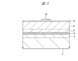
例えばGaAsからなる基板1の主面上には、下層から順にn型クラッド層2、活性層3、p型第1クラッド層4およびp型第2クラッド層5が積層されている。また、p型第2クラッド層5の一部には凸形の断面形状を有し、図1の紙面に垂直な方向に沿ってストライプ状に延在するリッジ部(リッジ導波路)5Aが形成されており、このリッジ部5Aの上面にはp型コンタクト層6が形成されている。
For example, an n-
これらの半導体層のうち、n型クラッド層2は、例えばAlGaInPで構成されており、活性層3は、例えばノンドープAlGaInPからなる障壁層とノンドープGaInPからなる井戸層とを交互に5層程度積層した多重量子井戸(Multi Quantum Well:MQW)構造で構成されている。また、p型第1クラッド層4は、例えばAlGaInPで構成されており、リッジ部5Aが形成されたp型第2クラッド層5は、例えばAlGaInP層で構成されている。さらに、p型コンタクト層6は、例えばGaAsで構成されている。そして、これらの半導体層と基板1とを合わせた合計の厚さは、例えば70〜130μmである。
Among these semiconductor layers, the n-
上記リッジ部5Aの両側壁およびリッジ部5Aの両側の平坦部(p型第2クラッド層5の上面)には、例えば酸化シリコンからなる第1パッシベーション膜8が形成されている。この第1パッシベーション膜8は、動作時に活性層3の近傍で発生する熱をリッジ部5Aから良好に放熱させるために、100nm以下の薄い膜厚で形成されている。
A
また、上記リッジ部5Aの側壁下部から、リッジ部5Aの側壁近傍のp型第2クラッド層5の上面に亘り、上記第1パッシベーション膜8を覆うように第2パッシベーション膜9が連続的に形成されている。すなわち、リッジ部5Aの側壁上部は、薄いパッシベーション膜(第1パッシベーション膜8)で覆われているのに対し、リッジ部5Aの側壁の下部と、リッジ部5Aに隣接するp型第2クラッド層5の上面は、厚いパッシベーション膜(第1パッシベーション膜8および第2パッシベーション膜9)で覆われている。
Further, the
上記第2パッシベーション膜9は、例えば窒化シリコン膜や酸化シリコン膜のように、第1パッシベーション膜8を構成する酸化シリコン膜とはエッチング選択比が異なる絶縁膜によって構成されている。また、リッジ部5Aの側壁底部における2層のパッシベーション膜(第1パッシベーション膜8および第2パッシベーション膜9)の合計の膜厚(図1に示すp型第2クラッド層6の表面からθ=45°方向の膜厚)は、150nm〜600nmである。
The
リッジ部5Aの側壁底部におけるパッシベーション膜の膜厚が150nm未満になると、電極に光が吸収されるため、スロープ効率が低下して高出力動作が困難になる。他方、リッジ部5Aの側壁底部におけるパッシベーション膜の膜厚が600nmを超えると、リッジ部5Aからの放熱特性が悪化し、キンクレベルが低下する。従って、リッジ部5Aの側壁底部におけるパッシベーション膜(第1パッシベーション膜8および第2パッシベーション膜9)の合計の膜厚は、150nm〜600nmの範囲とすることが望ましい。
If the thickness of the passivation film at the bottom of the side wall of the
p型コンタクト層6の上部にはp型電極10が形成されており、基板1の裏面にはn型電極11が形成されている。p型電極10およびn型電極11は、例えばTi膜の上部にPt膜およびAu膜を順次積層した金属膜からなる。
A p-
次に、図2〜図12を参照しながら、本実施の形態の半導体レーザ装置の製造方法の一例を説明する。 Next, an example of a method for manufacturing the semiconductor laser device of the present embodiment will be described with reference to FIGS.
まず、図2に示すように、MOCVD法(Metal Organic Chemical Vapor Deposition:有機金属成長法)を用いて基板1の主面上にn型クラッド層2、活性層3、p型第1クラッド層4、p型第2クラッド層5およびp型コンタクト層6を順次堆積した後、CVD法を用いて続いてp型コンタクト層6の上部に酸化シリコン膜12を堆積する。
First, as shown in FIG. 2, an n-
次に、図3に示すように、図示しないフォトレジスト膜をマスクにしたドライエッチングで酸化シリコン膜10の一部を除去した後、酸化シリコン膜12の上部のフォトレジスト膜をアッシングにより除去する。
Next, as shown in FIG. 3, after part of the
次に、図4に示すように、酸化シリコン膜12をマスクにしたウェットエッチングでp型コンタクト層6とp型第2クラッド層5の一部とを除去することにより、p型第2クラッド層5にリッジ部5Aを形成する。
Next, as shown in FIG. 4, the p-type second cladding layer is removed by removing the p-
次に、フッ酸(HF)系エッチング液を用いたウェットエッチングで酸化シリコン膜12を除去した後、図5に示すように、CVD法を用いて基板1の主面上に酸化シリコンからなる第1パッシベーション膜8および窒化シリコン膜(または酸化シリコン膜)からなる第2パッシベーション膜9を順次堆積する。前述したように、第1パッシベーション膜8は、100nm以下の薄い膜厚で堆積する。
Next, after the
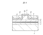
次に、図6に示すように、基板1の主面上にフォトレジスト膜13を塗布した後、その一部を選択的に露光・現像することにより、フォトレジスト膜13の上面をリッジ部5Aの上部に堆積された第2パッシベーション膜9の上面よりも下方に後退させる。
Next, as shown in FIG. 6, after a
次に、図7に示すように、フォトレジスト膜13をマスクにしたドライエッチングでリッジ部5Aの上部と側壁上部の第2パッシベーション膜9を除去する。
Next, as shown in FIG. 7, the
次に、図8に示すように、フォトレジスト膜13をマスクにしたドライエッチングでリッジ部5Aの上部の第1パッシベーション膜8を除去し、p型コンタクト層6の表面を露出させる。
Next, as shown in FIG. 8, the
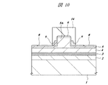
次に、フォトレジスト膜13を除去した後、図9に示すように、基板1の主面上にフォトレジスト膜14を塗布し、その一部を選択的に露光・現像することにより、リッジ部5Aの上部およびリッジ部5Aの側壁近傍の上部にフォトレジスト膜14を残す。
Next, after removing the
次に、図10に示すように、フォトレジスト膜14をマスクにしたドライエッチングで第2パッシベーション膜9の一部を除去し、リッジ部5Aの側壁下部およびリッジ部5Aの側壁近傍に第2パッシベーション膜9を残す。
Next, as shown in FIG. 10, a part of the
次に、フォトレジスト膜14を除去した後、図11に示すように、真空蒸着法を用いて基板1の主面上にTi膜、Pt膜およびAu膜を順次堆積し、続いてこれらの金属膜をエッチングすることによって、p型コンタクト層6の上部にp型電極10を形成する。
Next, after removing the
次に、基板1の裏面を研削して基板1の厚さを100μm程度まで薄くした後、真空蒸着法を用いて基板1の裏面にTi膜、Pt膜およびAu膜を順次堆積し、続いてこれらの金属膜をエッチングすることによって、n型電極11を形成する。これにより、図1に示す本実施の形態の半導体レーザ装置が完成する。
Next, the back surface of the
本実施の形態によれば、高い放熱性と高いスロープ効率を両立させることが可能となるので、半導体レーザ装置の高温・高出力特性を改善することができる。 According to the present embodiment, it is possible to achieve both high heat dissipation and high slope efficiency, so that the high temperature / high output characteristics of the semiconductor laser device can be improved.
(実施の形態2)
前記実施の形態1では、リッジ部5Aの側壁下部およびリッジ部5Aの側壁近傍に第2パッシベーション膜9を形成したが、例えば図12に示すように、リッジ部5Aの両側のp型第2クラッド層5の上面全体に第2パッシベーション膜9を形成してもよい。このような形状の第2パッシベーション膜9は、前記実施の形態1の図9および図10に示す工程を省略することによって形成することができる。
(Embodiment 2)
In the first embodiment, the
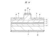
また、図13に示すように、前記実施の形態1の図7に示す工程でリッジ部5Aの上部と側壁上部の第2パッシベーション膜9を除去する際、リッジ部5Aの側壁下部に残す第2パッシベーション膜9の膜厚を、p型第2クラッド層5の上面に形成された第2パッシベーション膜9の膜厚と同程度にしてもよい。この場合も、図14に示すように、リッジ部5Aの両側のp型第2クラッド層5の上面全体に第2パッシベーション膜9を形成してもよい。
Further, as shown in FIG. 13, when the
また、前記実施の形態1では、第1パッシベーション膜8を酸化シリコン膜で構成し、第2パッシベーション膜9を窒化シリコン膜(または酸化シリコン膜)で構成したが、第1パッシベーション膜8および第2パッシベーション膜9の材料はこれらに限定されるものではない。
In the first embodiment, the
例えば図15に示すように、基板1の主面上にスピンコート法でポリイミド樹脂を塗布した後、このポリイミド樹脂をウェットエッチングすることによって、リッジ部5Aの側壁下部およびリッジ部5Aの側壁近傍に第2パッシベーション膜9を形成することもできる。この方法によれば、前記実施の形態1に比べて製造工程を大幅に短縮することができる。
For example, as shown in FIG. 15, after a polyimide resin is applied to the main surface of the
また、第1パッシベーション膜8および第2パッシベーション膜9は、同一の絶縁材料で構成することもできる。この場合は、第1パッシベーション膜8と第2パッシベーション膜9を異なる成膜方法で堆積し、エッチング選択比を変えることにより、前記実施の形態1と同様の製造方法を適用することが好ましい。また、一層の絶縁材料を第1パッシベーション膜8および第2パッシベーション膜9の合計の膜厚に相当する厚さに連続して形成した後、フォトリソグラフィプロセスとドライエッチングあるいはウェットエッチングとを駆使し、リッジ部5Aの側壁上部およびリッジ部5Aから離れた平坦部のパッシベーション膜の膜厚を、第1パッシベーション膜8に相当する厚さに薄くすることによっても本発明を実施できることはいうまでもない。
Also, the
さらに、第2パッシベーション膜9は、絶縁材料に限定されるものではなく、当該レーザの発振波長帯で光吸収が小さい透明導電材料で構成することもできる。
Furthermore, the
以上、本発明者によってなされた発明を実施の形態に基づき具体的に説明したが、本発明は前記実施の形態に限定されるものではなく、その要旨を逸脱しない範囲で種々変更可能であることはいうまでもない。 As mentioned above, the invention made by the present inventor has been specifically described based on the embodiment. However, the present invention is not limited to the embodiment, and various modifications can be made without departing from the scope of the invention. Needless to say.
本発明は、半導体レーザ装置の高温・高出力特性の改善に適用することができる。 The present invention can be applied to the improvement of high temperature and high output characteristics of a semiconductor laser device.
1 基板(半導体基板)
2 n型クラッド層
3 活性層
4 p型第1クラッド層
5 p型第2クラッド層
5A リッジ部
6 p型コンタクト層
8 第1パッシベーション膜
9 第2パッシベーション膜
10 p型電極
11 n型電極
12 酸化シリコン膜
13、14 フォトレジスト膜
1 Substrate (semiconductor substrate)
2 n-
Claims (5)
前記リッジ部の両側壁、および前記リッジ部の両側の前記p型第2クラッド層の上面には、第1パッシベーション膜が形成されており、
前記リッジ部の側壁上部を除く前記リッジ部の側壁下部、および前記リッジ部の側壁近傍の前記p型第2クラッド層の上面には、前記第1パッシベーション膜の少なくとも一部を覆うように第2パッシベーション膜が形成され、
前記第2パッシベーション膜のうち前記リッジ部の側壁近傍に設けられる部分は、前記p型第2クラッド層の積層方向に厚みを有することを特徴とする半導体レーザ装置。 At least an n-type cladding layer, an active layer, a p-type first cladding layer, and a p-type second cladding layer are stacked on the main surface of the semiconductor substrate, and a convex cross-sectional shape is formed on a part of the p-type second cladding layer. A semiconductor laser device in which a striped ridge portion is formed,
A first passivation film is formed on both side walls of the ridge portion and on the upper surface of the p-type second cladding layer on both sides of the ridge portion,
A second lower portion of the first passivation film is covered on the lower portion of the side wall of the ridge portion excluding the upper portion of the side wall of the ridge portion and on the upper surface of the p-type second cladding layer in the vicinity of the side wall of the ridge portion. A passivation film is formed,
A portion of the second passivation film provided in the vicinity of the side wall of the ridge portion has a thickness in the stacking direction of the p-type second cladding layer.
前記リッジ部の両側壁、および前記リッジ部の両側の前記p型第2クラッド層の上面には、第1パッシベーション膜が形成されており、
前記リッジ部の側壁下部、および前記リッジ部の側壁近傍の前記p型第2クラッド層の上面には、前記第1パッシベーション膜を覆うように第2パッシベーション膜が形成され、
前記第1パッシベーション膜と前記第2パッシベーション膜は、同一の絶縁材料からなることを特徴とする半導体レーザ装置。 At least an n-type cladding layer, an active layer, a p-type first cladding layer, and a p-type second cladding layer are stacked on the main surface of the semiconductor substrate, and a convex cross-sectional shape is formed on a part of the p-type second cladding layer. A semiconductor laser device in which a striped ridge portion is formed,
A first passivation film is formed on both side walls of the ridge portion and on the upper surface of the p-type second cladding layer on both sides of the ridge portion,
A second passivation film is formed so as to cover the first passivation film on the lower portion of the sidewall of the ridge portion and on the upper surface of the p-type second cladding layer in the vicinity of the sidewall of the ridge portion,
The semiconductor laser device, wherein the first passivation film and the second passivation film are made of the same insulating material.
前記リッジ部の両側壁、および前記リッジ部の両側の前記p型第2クラッド層の上面には、第1パッシベーション膜が形成されており、
前記リッジ部の側壁下部、および前記リッジ部の側壁近傍の前記p型第2クラッド層の上面には、前記第1パッシベーション膜を覆うように第2パッシベーション膜が形成され、
前記第1パッシベーション膜は第1絶縁膜からなり、前記第2パッシベーション膜は、第1導電膜からなることを特徴とする半導体レーザ装置。 At least an n-type cladding layer, an active layer, a p-type first cladding layer, and a p-type second cladding layer are stacked on the main surface of the semiconductor substrate, and a convex cross-sectional shape is formed on a part of the p-type second cladding layer. A semiconductor laser device in which a striped ridge portion is formed,
A first passivation film is formed on both side walls of the ridge portion and on the upper surface of the p-type second cladding layer on both sides of the ridge portion,
A second passivation film is formed so as to cover the first passivation film on the lower portion of the sidewall of the ridge portion and on the upper surface of the p-type second cladding layer in the vicinity of the sidewall of the ridge portion,
The semiconductor laser device, wherein the first passivation film is made of a first insulating film, and the second passivation film is made of a first conductive film.
Priority Applications (1)
| Application Number | Priority Date | Filing Date | Title |
|---|---|---|---|
| JP2011100480A JP5872790B2 (en) | 2011-04-28 | 2011-04-28 | Semiconductor laser device |
Applications Claiming Priority (1)
| Application Number | Priority Date | Filing Date | Title |
|---|---|---|---|
| JP2011100480A JP5872790B2 (en) | 2011-04-28 | 2011-04-28 | Semiconductor laser device |
Publications (3)
| Publication Number | Publication Date |
|---|---|
| JP2012234862A JP2012234862A (en) | 2012-11-29 |
| JP2012234862A5 JP2012234862A5 (en) | 2014-05-01 |
| JP5872790B2 true JP5872790B2 (en) | 2016-03-01 |
Family
ID=47434934
Family Applications (1)
| Application Number | Title | Priority Date | Filing Date |
|---|---|---|---|
| JP2011100480A Active JP5872790B2 (en) | 2011-04-28 | 2011-04-28 | Semiconductor laser device |
Country Status (1)
| Country | Link |
|---|---|
| JP (1) | JP5872790B2 (en) |
Families Citing this family (3)
| Publication number | Priority date | Publication date | Assignee | Title |
|---|---|---|---|---|
| JP6388838B2 (en) * | 2015-03-09 | 2018-09-12 | Nttエレクトロニクス株式会社 | Optical functional element |
| JP6981492B2 (en) * | 2018-08-20 | 2021-12-15 | 三菱電機株式会社 | Manufacturing method of semiconductor laser device |
| WO2020039475A1 (en) | 2018-08-20 | 2020-02-27 | 三菱電機株式会社 | Semiconductor laser device manufacturing method and semiconductor laser device |
Family Cites Families (8)
| Publication number | Priority date | Publication date | Assignee | Title |
|---|---|---|---|---|
| JP4111696B2 (en) * | 2001-08-08 | 2008-07-02 | 三洋電機株式会社 | Nitride semiconductor laser device |
| JP2006012899A (en) * | 2004-06-22 | 2006-01-12 | Sharp Corp | Semiconductor laser device and its manufacturing method |
| JP4952184B2 (en) * | 2005-11-01 | 2012-06-13 | 日亜化学工業株式会社 | Nitride semiconductor laser device and manufacturing method thereof |
| JP2007134445A (en) * | 2005-11-09 | 2007-05-31 | Nichia Chem Ind Ltd | Nitride semiconductor laser device |
| JP2007311682A (en) * | 2006-05-22 | 2007-11-29 | Matsushita Electric Ind Co Ltd | Semiconductor device |
| JP4985374B2 (en) * | 2006-12-28 | 2012-07-25 | 日亜化学工業株式会社 | Nitride semiconductor laser device |
| US8073031B2 (en) * | 2008-03-03 | 2011-12-06 | Sharp Kabushiki Kaisha | Laser diode with improved heat dissipation |
| JP5343687B2 (en) * | 2009-04-28 | 2013-11-13 | 日亜化学工業株式会社 | Nitride semiconductor laser device |
-
2011
- 2011-04-28 JP JP2011100480A patent/JP5872790B2/en active Active
Also Published As
| Publication number | Publication date |
|---|---|
| JP2012234862A (en) | 2012-11-29 |
Similar Documents
| Publication | Publication Date | Title |
|---|---|---|
| JP4850453B2 (en) | Semiconductor light emitting device manufacturing method and semiconductor light emitting device | |
| JP6495921B2 (en) | Semiconductor laser diode, method for manufacturing semiconductor laser diode, and semiconductor laser diode device | |
| JP6829497B2 (en) | Nitride semiconductor light emitting device and its manufacturing method | |
| JP5742325B2 (en) | Semiconductor laser device and manufacturing method thereof | |
| JP6094632B2 (en) | Semiconductor laser element | |
| JP2010074131A (en) | Semiconductor light emitting device and method for manufacturing same | |
| JP2010186791A (en) | Semiconductor light-emitting element, and method for manufacturing the same | |
| JP2006128617A (en) | Semiconductor laser element and its manufacturing method | |
| JP5872790B2 (en) | Semiconductor laser device | |
| JP5307300B2 (en) | Optical device, optical device manufacturing method, and laser module | |
| JP2009212386A (en) | Method of manufacturing semiconductor light element | |
| JP2008042131A (en) | Semiconductor optical element, and manufacturing method thereof | |
| JP3928695B2 (en) | Surface emitting semiconductor light emitting device and method of manufacturing the same | |
| JP2020126995A (en) | Semiconductor laser element and manufacturing method of the same | |
| JP2008300802A (en) | Semiconductor laser element and method of manufacturing same | |
| JP2010238715A (en) | Method for manufacturing semiconductor light-emitting element, and semiconductor light-emitting element | |
| JP5319623B2 (en) | Semiconductor light emitting device | |
| JP6140101B2 (en) | Semiconductor optical device | |
| JP4090337B2 (en) | Semiconductor laser device and method for manufacturing semiconductor laser device | |
| JP5292443B2 (en) | Method for manufacturing optical semiconductor element | |
| JP2010205829A (en) | Semiconductor light-emitting element, and method for manufacturing the same | |
| JP2019102492A (en) | Semiconductor laser element and semiconductor laser device | |
| US20070026550A1 (en) | Method of manufacturing semiconductor light emitting apparatus and semiconductor light emitting apparatus | |
| JP2013219238A (en) | Superconductive device | |
| JP2012204671A (en) | Semiconductor light-emitting element |
Legal Events
| Date | Code | Title | Description |
|---|---|---|---|
| RD02 | Notification of acceptance of power of attorney |
Free format text: JAPANESE INTERMEDIATE CODE: A7422 Effective date: 20121214 |
|
| RD04 | Notification of resignation of power of attorney |
Free format text: JAPANESE INTERMEDIATE CODE: A7424 Effective date: 20121220 |
|
| A521 | Request for written amendment filed |
Free format text: JAPANESE INTERMEDIATE CODE: A523 Effective date: 20140317 |
|
| A621 | Written request for application examination |
Free format text: JAPANESE INTERMEDIATE CODE: A621 Effective date: 20140317 |
|
| A711 | Notification of change in applicant |
Free format text: JAPANESE INTERMEDIATE CODE: A711 Effective date: 20141031 |
|
| A977 | Report on retrieval |
Free format text: JAPANESE INTERMEDIATE CODE: A971007 Effective date: 20141217 |
|
| A131 | Notification of reasons for refusal |
Free format text: JAPANESE INTERMEDIATE CODE: A131 Effective date: 20150106 |
|
| A521 | Request for written amendment filed |
Free format text: JAPANESE INTERMEDIATE CODE: A523 Effective date: 20150305 |
|
| A131 | Notification of reasons for refusal |
Free format text: JAPANESE INTERMEDIATE CODE: A131 Effective date: 20150714 |
|
| A521 | Request for written amendment filed |
Free format text: JAPANESE INTERMEDIATE CODE: A523 Effective date: 20150908 |
|
| TRDD | Decision of grant or rejection written | ||
| A01 | Written decision to grant a patent or to grant a registration (utility model) |
Free format text: JAPANESE INTERMEDIATE CODE: A01 Effective date: 20151222 |
|
| A61 | First payment of annual fees (during grant procedure) |
Free format text: JAPANESE INTERMEDIATE CODE: A61 Effective date: 20160114 |
|
| R150 | Certificate of patent or registration of utility model |
Ref document number: 5872790 Country of ref document: JP Free format text: JAPANESE INTERMEDIATE CODE: R150 |
|
| S531 | Written request for registration of change of domicile |
Free format text: JAPANESE INTERMEDIATE CODE: R313531 |
|
| R360 | Written notification for declining of transfer of rights |
Free format text: JAPANESE INTERMEDIATE CODE: R360 |
|
| R350 | Written notification of registration of transfer |
Free format text: JAPANESE INTERMEDIATE CODE: R350 |
|
| R250 | Receipt of annual fees |
Free format text: JAPANESE INTERMEDIATE CODE: R250 |
|
| R250 | Receipt of annual fees |
Free format text: JAPANESE INTERMEDIATE CODE: R250 |
|
| R250 | Receipt of annual fees |
Free format text: JAPANESE INTERMEDIATE CODE: R250 |
|
| R250 | Receipt of annual fees |
Free format text: JAPANESE INTERMEDIATE CODE: R250 |
|
| R250 | Receipt of annual fees |
Free format text: JAPANESE INTERMEDIATE CODE: R250 |
|
| R250 | Receipt of annual fees |
Free format text: JAPANESE INTERMEDIATE CODE: R250 |