JP5870258B2 - Light bulb shaped lamp and lighting device - Google Patents

Light bulb shaped lamp and lighting device Download PDF

Info

Publication number
JP5870258B2
JP5870258B2 JP2011113998A JP2011113998A JP5870258B2 JP 5870258 B2 JP5870258 B2 JP 5870258B2 JP 2011113998 A JP2011113998 A JP 2011113998A JP 2011113998 A JP2011113998 A JP 2011113998A JP 5870258 B2 JP5870258 B2 JP 5870258B2
Authority
JP
Japan
Prior art keywords
substrate
globe
light emitting
filling member
light
Prior art date
Legal status (The legal status is an assumption and is not a legal conclusion. Google has not performed a legal analysis and makes no representation as to the accuracy of the status listed.)
Expired - Fee Related
Application number
JP2011113998A
Other languages
Japanese (ja)
Other versions
JP2012243643A (en
Inventor
次弘 松田
次弘 松田
延吉 竹内
延吉 竹内
隆在 植本
隆在 植本
三貴 政弘
政弘 三貴
Current Assignee (The listed assignees may be inaccurate. Google has not performed a legal analysis and makes no representation or warranty as to the accuracy of the list.)
Panasonic Intellectual Property Management Co Ltd
Original Assignee
Panasonic Intellectual Property Management Co Ltd
Priority date (The priority date is an assumption and is not a legal conclusion. Google has not performed a legal analysis and makes no representation as to the accuracy of the date listed.)
Filing date
Publication date
Application filed by Panasonic Intellectual Property Management Co Ltd filed Critical Panasonic Intellectual Property Management Co Ltd
Priority to JP2011113998A priority Critical patent/JP5870258B2/en
Publication of JP2012243643A publication Critical patent/JP2012243643A/en
Application granted granted Critical
Publication of JP5870258B2 publication Critical patent/JP5870258B2/en
Expired - Fee Related legal-status Critical Current
Anticipated expiration legal-status Critical

Links

Images

Classifications

    • FMECHANICAL ENGINEERING; LIGHTING; HEATING; WEAPONS; BLASTING
    • F21LIGHTING
    • F21VFUNCTIONAL FEATURES OR DETAILS OF LIGHTING DEVICES OR SYSTEMS THEREOF; STRUCTURAL COMBINATIONS OF LIGHTING DEVICES WITH OTHER ARTICLES, NOT OTHERWISE PROVIDED FOR
    • F21V29/00Protecting lighting devices from thermal damage; Cooling or heating arrangements specially adapted for lighting devices or systems
    • F21V29/50Cooling arrangements
    • F21V29/56Cooling arrangements using liquid coolants
    • F21V29/58Cooling arrangements using liquid coolants characterised by the coolants
    • FMECHANICAL ENGINEERING; LIGHTING; HEATING; WEAPONS; BLASTING
    • F21LIGHTING
    • F21KNON-ELECTRIC LIGHT SOURCES USING LUMINESCENCE; LIGHT SOURCES USING ELECTROCHEMILUMINESCENCE; LIGHT SOURCES USING CHARGES OF COMBUSTIBLE MATERIAL; LIGHT SOURCES USING SEMICONDUCTOR DEVICES AS LIGHT-GENERATING ELEMENTS; LIGHT SOURCES NOT OTHERWISE PROVIDED FOR
    • F21K9/00Light sources using semiconductor devices as light-generating elements, e.g. using light-emitting diodes [LED] or lasers
    • F21K9/20Light sources comprising attachment means
    • F21K9/23Retrofit light sources for lighting devices with a single fitting for each light source, e.g. for substitution of incandescent lamps with bayonet or threaded fittings
    • F21K9/232Retrofit light sources for lighting devices with a single fitting for each light source, e.g. for substitution of incandescent lamps with bayonet or threaded fittings specially adapted for generating an essentially omnidirectional light distribution, e.g. with a glass bulb
    • FMECHANICAL ENGINEERING; LIGHTING; HEATING; WEAPONS; BLASTING
    • F21LIGHTING
    • F21YINDEXING SCHEME ASSOCIATED WITH SUBCLASSES F21K, F21L, F21S and F21V, RELATING TO THE FORM OR THE KIND OF THE LIGHT SOURCES OR OF THE COLOUR OF THE LIGHT EMITTED
    • F21Y2115/00Light-generating elements of semiconductor light sources
    • F21Y2115/10Light-emitting diodes [LED]

Description

本発明は、半導体発光素子を備える電球形ランプ及びこれを備える照明装置に関する。   The present invention relates to a light bulb shaped lamp including a semiconductor light emitting element and an illumination device including the same.

半導体発光素子である発光ダイオード(LED:Light Emitting Diode)は、従来の照明光源に比べて、小型、高効率及び長寿命である。近年の省エネあるいは省資源に対する市場ニーズが追い風となり、フィラメントコイルを用いた従来の白熱電球の代替えとなるランプとして、LEDを用いた電球形ランプ(以下、単に「LED電球」ともいう)の需要が増加している。   A light emitting diode (LED), which is a semiconductor light emitting element, is smaller, more efficient, and has a longer life than a conventional illumination light source. Market demand for energy saving or resource saving in recent years has been a tailwind, and there is a demand for light bulb shaped lamps using LEDs (hereinafter also simply referred to as “LED bulbs”) as lamps that can replace conventional incandescent bulbs using filament coils. It has increased.

LEDは、その温度が上昇するに伴って光出力が低下して、寿命が短くなることが知られている。そこで、LEDの温度上昇を抑制するために、従来のLED電球では、半球状のグローブと口金との間に金属製の筐体が設けられている(例えば、特許文献1を参照)。   It is known that the light output of an LED decreases as its temperature rises, and its life is shortened. Therefore, in order to suppress the temperature rise of the LED, in the conventional LED bulb, a metal housing is provided between the hemispherical globe and the base (for example, see Patent Document 1).

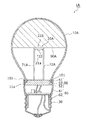
以下、特許文献1に開示された従来の電球形LEDランプ400について、図13を用いて説明する。図13は、従来に係る電球形LEDランプの断面図である。   Hereinafter, a conventional bulb-type LED lamp 400 disclosed in Patent Document 1 will be described with reference to FIG. FIG. 13 is a cross-sectional view of a conventional bulb-type LED lamp.

図13に示すように、従来の電球形LEDランプ400は、半球状のグローブである透光性のカバー410、受電用の口金420及び金属性筐体である外郭部材430を備える。   As shown in FIG. 13, a conventional light bulb-shaped LED lamp 400 includes a translucent cover 410 that is a hemispherical glove, a base 420 for receiving power, and an outer member 430 that is a metallic casing.

外郭部材430は、外部に露出する周部431と、この周部431に一体に形成された円板状の光源取り付け部432と、周部431の内側に形成された凹部433とを有する。光源取り付け部432の上面には、複数のLEDを備えるLEDモジュール440が取り付けられている。なお、凹部433の内面には、その内面形状に沿って形成された絶縁部材450が設けられており、絶縁部材450の内部には、LEDを点灯させるための点灯回路460が収容されている。   The outer member 430 includes a peripheral portion 431 exposed to the outside, a disk-shaped light source mounting portion 432 formed integrally with the peripheral portion 431, and a concave portion 433 formed inside the peripheral portion 431. An LED module 440 including a plurality of LEDs is attached to the upper surface of the light source attachment portion 432. An insulating member 450 formed along the inner surface shape is provided on the inner surface of the recess 433, and a lighting circuit 460 for lighting the LED is accommodated in the insulating member 450.

このように構成された従来の電球形LEDランプ400によれば、光源取り付け部432と周部431とが一体に成型された外郭部材430を用いているので、LEDで発生した熱を光源取り付け部432から周部431に向かって効率良く熱伝導させることができる。これにより、LEDの温度上昇が抑制されるので、LEDの光出力の低下を防止することができる。   According to the conventional light bulb shaped LED lamp 400 configured as described above, since the outer member 430 in which the light source mounting portion 432 and the peripheral portion 431 are integrally formed is used, the heat generated by the LED is used as the light source mounting portion. Heat conduction can be efficiently performed from 432 toward the peripheral portion 431. Thereby, since the temperature rise of LED is suppressed, the fall of the light output of LED can be prevented.

特開2006−313717号公報JP 2006-313717 A

しかし、特許文献1に開示された従来に係る電球形LEDランプ400では、LEDモジュール440が外郭部材430に配置されており、外郭部材430の凹部433の内面形状に沿って点灯回路460が配置されている。これにより、LEDモジュール440において発生した熱が受電用の口金420側に伝わりやすく、例えば点灯回路460に不具合が発生しやすくなるという問題がある。このように、口金420側は、電力の供給を受ける部分であり、従来の構成では放熱が不十分であった。   However, in the conventional bulb-type LED lamp 400 disclosed in Patent Document 1, the LED module 440 is disposed on the outer member 430, and the lighting circuit 460 is disposed along the inner surface shape of the recess 433 of the outer member 430. ing. Thereby, the heat generated in the LED module 440 is likely to be transmitted to the power receiving base 420 side, and there is a problem that, for example, the lighting circuit 460 is likely to malfunction. As described above, the base 420 side is a portion that receives supply of electric power, and heat radiation is insufficient in the conventional configuration.

本発明は、このような問題を解決するためになされたものであり、LEDモジュールにおいて発生した熱を十分に放熱することができる電球形ランプ及びそれを備える照明装置を提供することを目的とする。   The present invention has been made to solve such a problem, and an object of the present invention is to provide a light bulb shaped lamp capable of sufficiently dissipating heat generated in an LED module and an illumination device including the same. .

上記目的を達成するために、本発明の一態様に係る電球形ランプは、中空のグローブと、基板と、前記基板に実装された半導体発光素子とを有する発光モジュールと、前記半導体発光素子を発光させるための電力を受電する受電部と、前記発光モジュールを挟んで前記受電部とは反対側において、前記グローブと前記基板とを熱的に接続する充填部材と、を備え、前記充填部材は、前記反対側において前記グローブの内面と接しており、前記受電部側の面が前記グローブの中空の空間に開放されており、前記発光モジュールは、一部が前記充填部材の前記受電部側の面に接しており、他の部分が前記グローブの中空の空間に開放されているIn order to achieve the above object, a light bulb shaped lamp according to one embodiment of the present invention includes a light emitting module having a hollow globe, a substrate, and a semiconductor light emitting element mounted on the substrate, and emits light from the semiconductor light emitting element. A power receiving unit that receives power for powering, and a filling member that thermally connects the globe and the substrate on a side opposite to the power receiving unit across the light emitting module, and the filling member includes: The surface on the opposite side is in contact with the inner surface of the globe, the surface on the power receiving unit side is open to the hollow space of the globe, and the light emitting module is partly on the surface on the power receiving unit side of the filling member The other part is open to the hollow space of the globe .

この構成により、発光モジュールにおいて発生した熱を、受電部が配置される固定部材側から放熱させるだけでなく、その反対側の充填部材側からグローブに伝導させて、グローブから放熱させることができる。これにより、受電部とは反対側へ発光モジュールから生じた熱を逃がすことができ、十分に放熱することができる。   With this configuration, heat generated in the light emitting module can be radiated not only from the fixing member side where the power receiving unit is disposed, but also from the opposite filling member side to the globe and radiated from the globe. Thereby, the heat generated from the light emitting module can be released to the side opposite to the power receiving unit, and the heat can be sufficiently radiated.

た、本発明の一態様に係る電球形ランプ中空のグローブと、基板と、前記基板に実装された半導体発光素子とを有する発光モジュールと、前記半導体発光素子を発光させるための電力を受電する受電部と、前記発光モジュールを挟んで前記受電部とは反対側において、前記グローブと前記基板とを熱的に接続する充填部材と、前記受電部側から延びており、前記発光モジュールを固定するための固定部材と、を備え、前記充填部材は、前記反対側において前記グローブの内面と接しており、前記受電部側の面が前記グローブの中空の空間に開放されており、前記基板は、長尺矩形状の板状基板であり、一端が前記充填部材のうち前記中空の空間に開放されている面に固定され、他端が前記固定部材に立設されて固定される。
さらに、本発明の一態様に係る電球形ランプにおいて、前記充填部材は、透光性を有する透光性材料から成ることが好ましい。
Also, the light bulb-shaped lamp according to one embodiment of the present invention includes a hollow globe, a substrate, a light emitting module having a semiconductor light emitting element mounted on the substrate, the electric power for emitting the semiconductor light emitting element A power receiving unit that receives power, a filling member that thermally connects the globe and the substrate on a side opposite to the power receiving unit across the light emitting module, and extending from the power receiving unit side, and the light emitting module and a fixing member for fixing said filler member in the opposite is in contact with the inner surface of the glove, the surface of the power receiving portion side is open to the hollow space of the glove, the substrate is an elongated rectangular plate-like substrate, one end of which is fixed to a surface which is open to the hollow space of the packing member, the other end Ru is fixedly erected on the fixing member.
Furthermore, in the light bulb shaped lamp according to one aspect of the present invention, it is preferable that the filling member is made of a translucent material having translucency.

この構成により、発光モジュールから発光した光を充填部材が透光させることができるため、充填部材を配置しても受電部とは反対側へ所定光を放出させることができる。   With this configuration, since the filling member can transmit light emitted from the light emitting module, predetermined light can be emitted to the side opposite to the power receiving unit even if the filling member is disposed.

さらに、本発明の一態様に係る電球形ランプにおいて、前記充填部材は、前記反対側において前記グローブの中空の空間の一部を充填することが好ましい。
Furthermore, the bulb-type lamp according to one embodiment of the present invention, the filling member is preferably Hama part of the hollow space of the glove at the opposite charge.

この構成により、充填部材がグローブの中空空間の一部を少なくとも充填するため、充填部材が接しているグローブへの発光モジュールにおいて発生した熱を伝導させて、グローブから放熱させることができる。   With this configuration, since the filling member fills at least a part of the hollow space of the globe, the heat generated in the light emitting module to the globe in contact with the filling member can be conducted and released from the globe.

さらに、本発明の一態様に係る電球形ランプにおいて、前記基板は、長尺矩形状の板状基板であり、一端が前記充填部材に接続されることが好ましい。また、本発明の一態様に係る電球形ランプにおいて、さらに、前記受電部側から延びており、前記発光モジュールを固定するための固定部材を備え、前記基板は、他端が前記固定部材に立設されて固定されることが好ましい。   Furthermore, in the light bulb shaped lamp according to an aspect of the present invention, it is preferable that the substrate is a long rectangular plate-shaped substrate, and one end is connected to the filling member. The light bulb shaped lamp according to one aspect of the present invention further includes a fixing member that extends from the power receiving unit side and fixes the light emitting module, and the other end of the substrate stands on the fixing member. It is preferable to be installed and fixed.

この構成により、確実に発光モジュールを所定の位置に固定することができる。   With this configuration, the light emitting module can be reliably fixed at a predetermined position.

また、本発明の一態様に係る電球形ランプ中空のグローブと、基板と、前記基板に実装された半導体発光素子とを有する発光モジュールと、前記半導体発光素子を発光させるための電力を受電する受電部と、前記発光モジュールを挟んで前記受電部とは反対側において、前記グローブと前記基板とを熱的に接続する充填部材と、を備え、前記充填部材は、前記反対側において前記グローブの内面と接しており、前記受電部側の面が前記グローブの中空の空間に開放されており、前記発光モジュールは、前記基板の第1の主面または前記第1の主面とは反対側の第2の主面が、前記充填部材の前記受電部側の表面に沿って配置され、当該表面に対して接触する。 The self-ballasted lamp according to one embodiment of the present invention, receiving a hollow globe, a substrate, a light emitting module having a semiconductor light emitting element mounted on the substrate, the electric power for emitting the semiconductor light emitting element And a filling member that thermally connects the globe and the substrate on a side opposite to the power reception unit across the light emitting module, and the filling member is provided on the opposite side of the globe. The power receiving unit side surface is open to the hollow space of the globe, and the light emitting module is the first main surface of the substrate or the side opposite to the first main surface. the second major surface of, are arranged along the receiving side of the surface of the filling member, contact with the surface.

この構成により、発光モジュールの基板の端部だけでなく第1の主面または第2の主面の全てが充填部材と接触して接続されるため、より多くの発光モジュールにおいて発生した熱を充填部材に熱伝導させ、グローブから放熱させることができる。   With this configuration, not only the end portion of the substrate of the light emitting module but also all of the first main surface or the second main surface are connected in contact with the filling member, so that the heat generated in more light emitting modules is filled. Heat can be conducted to the member, and heat can be released from the globe.

また、本発明の一態様に係る電球形ランプ中空のグローブと、基板と、前記基板に実装された半導体発光素子とを有する発光モジュールと、前記半導体発光素子を発光させるための電力を受電する受電部と、前記発光モジュールを挟んで前記受電部とは反対側において、前記グローブと前記基板とを熱的に接続する充填部材と、を備え、前記充填部材は、前記反対側において前記グローブの内面と接しており、前記受電部側の面が前記グローブの中空の空間に開放されており、前記発光モジュールは、前記充填部材の内部に配置される。 The self-ballasted lamp according to one embodiment of the present invention, receiving a hollow globe, a substrate, a light emitting module having a semiconductor light emitting element mounted on the substrate, the electric power for emitting the semiconductor light emitting element And a filling member that thermally connects the globe and the substrate on a side opposite to the power reception unit across the light emitting module, and the filling member is provided on the opposite side of the globe. in contact with the inner surface, the surface of the power receiving portion side is open to the hollow space of the glove, the light emitting module, Ru is disposed in the filling member.

この構成により、発光モジュールにおいて発生した熱のほとんどが充填部材に熱伝導されることになる。充填部材は、大部分がグローブに接触しているため、グローブから熱を放熱させることができる。   With this configuration, most of the heat generated in the light emitting module is thermally conducted to the filling member. Since most of the filling member is in contact with the globe, heat can be dissipated from the globe.

さらに、本発明の一態様に係る電球形ランプにおいて、前記充填部材は、前記発光モジュールと前記グローブとを接着する接着材であることが好ましい。 Furthermore, in the light bulb shaped lamp according to one aspect of the present invention, the filling member is preferably an adhesive that bonds the light emitting module and the globe.

この構成により、接着材を介して発光モジュールをグローブに直に接続させることができるため、発光モジュールにおいて発生した熱を効率よくグローブから放熱させることができる。   With this configuration, since the light emitting module can be directly connected to the globe via the adhesive, the heat generated in the light emitting module can be efficiently radiated from the globe.

さらに、本発明の一態様に係る電球形ランプにおいて、前記充填部材は、熱伝導フィラーが添加されて成ることが好ましい。   Furthermore, in the light bulb shaped lamp according to one aspect of the present invention, it is preferable that the filling member is added with a heat conductive filler.

この構成により、充填部材における熱伝導性を向上させることができるため、発光モジュールにおいて発生した熱を効率よく放熱させることができる。   With this configuration, since the thermal conductivity in the filling member can be improved, the heat generated in the light emitting module can be efficiently radiated.

また、本発明の一態様に係る電球形ランプにおいて、さらに、前記受電部から受電した交流電力を直流電力に変換し、前記半導体発光素子に当該直流電力を供給する点灯回路を備えることが好ましい。   The light bulb shaped lamp according to one embodiment of the present invention preferably further includes a lighting circuit that converts AC power received from the power receiving unit into DC power, and supplies the DC power to the semiconductor light emitting element.

このように、点灯回路とは反対側へ発光モジュールから生じた熱を逃がすことができ、点灯回路への発光モジュールの発熱によるダメージを軽減することができる。   In this way, heat generated from the light emitting module can be released to the side opposite to the lighting circuit, and damage due to heat generation of the light emitting module to the lighting circuit can be reduced.

また、本発明の一態様に係る照明装置は、本発明の一態様に係る電球形ランプを備えるものである。   The lighting device according to one embodiment of the present invention includes the light bulb shaped lamp according to one embodiment of the present invention.

このように、本発明は、上記の電球形ランプを備える照明装置として実現することもできる。   Thus, this invention can also be implement | achieved as an illuminating device provided with said lightbulb-shaped lamp.

本発明によれば、LEDモジュールにおいて発生した熱を点灯回路に影響しないように放熱することができる。   According to the present invention, heat generated in the LED module can be dissipated without affecting the lighting circuit.

図1は、本発明の第1の実施形態に係る電球形ランプの斜視図である。FIG. 1 is a perspective view of a light bulb shaped lamp according to a first embodiment of the present invention. 図2は、本発明の第1の実施形態に係る電球形ランプの分解斜視図である。FIG. 2 is an exploded perspective view of the light bulb shaped lamp according to the first embodiment of the present invention. 図3は、本発明の第1の実施形態に係る電球形ランプの断面図である。FIG. 3 is a cross-sectional view of the light bulb shaped lamp according to the first embodiment of the present invention. 図4(a)は、本発明の第1の実施形態に係る電球形ランプにおけるLEDモジュールの正面図であり、図4(b)は、同LEDモジュールの側面図であり、図4(c)は、同LEDモジュールの断面図である。4 (a) is a front view of the LED module in the light bulb shaped lamp according to the first embodiment of the present invention, FIG. 4 (b) is a side view of the LED module, and FIG. 4 (c). These are sectional drawings of the LED module. 図5は、本発明の第2の実施形態に係る電球形ランプの断面図である。FIG. 5 is a sectional view of a light bulb shaped lamp according to the second embodiment of the present invention. 図6は、本発明の第2の実施形態の他の形態に係る電球形ランプの断面図である。FIG. 6 is a cross-sectional view of a light bulb shaped lamp according to another embodiment of the second embodiment of the present invention. 図7は、本発明の第3の実施形態に係る電球形ランプの断面図である。FIG. 7 is a cross-sectional view of a light bulb shaped lamp according to the third embodiment of the present invention. 図8は、本発明の第4の実施形態に係る電球形ランプの断面図である。FIG. 8 is a sectional view of a light bulb shaped lamp according to the fourth embodiment of the present invention. 図9は、本発明の第5の実施形態に係る電球形ランプの断面図である。FIG. 9 is a cross-sectional view of a light bulb shaped lamp according to the fifth embodiment of the present invention. 図10は、本発明の第5の実施形態に係る電球形ランプの断面図である。FIG. 10 is a sectional view of a light bulb shaped lamp according to the fifth embodiment of the present invention. 図11は、本発明の実施形態に係る照明装置の概略断面図である。FIG. 11 is a schematic cross-sectional view of a lighting device according to an embodiment of the present invention. 図12は、本発明の実施形態に係る他の照明装置の概略図である。FIG. 12 is a schematic view of another illumination device according to the embodiment of the present invention. 図13は、従来に係る電球形LEDランプの断面図である。FIG. 13 is a cross-sectional view of a conventional bulb-type LED lamp.

(第1の実施形態)
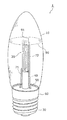
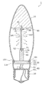
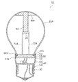
図1〜図3に示すように、本発明の第1の実施形態に係る電球形ランプ1は、白熱電球に代替する電球形のLEDランプであって、透光性のグローブ10と、LEDモジュール20と、受電用の口金30と、LEDモジュール20を固定する固定部材40とを備える。さらに、本実施形態に係る電球形ランプ1は、支持部材50と、樹脂ケース60と、第1のリード線71及び第2のリード線72と、点灯回路80と、充填部材90とを備える。本実施形態において、電球形ランプ1は、グローブ10と、樹脂ケース60と、口金30とによって外囲器が構成されている。
(First embodiment)
As shown in FIGS. 1 to 3, a light bulb shaped lamp 1 according to a first embodiment of the present invention is a light bulb shaped LED lamp that replaces an incandescent light bulb, and includes a translucent globe 10 and an LED module. 20, a base 30 for receiving power, and a fixing member 40 for fixing the LED module 20. Furthermore, the light bulb shaped lamp 1 according to the present embodiment includes a support member 50, a resin case 60, a first lead wire 71 and a second lead wire 72, a lighting circuit 80, and a filling member 90. In the present embodiment, the bulb-shaped lamp 1 includes an envelope formed by the globe 10, the resin case 60, and the base 30.

以下、本発明の第1の実施形態に係る電球形ランプ1の各構成要素について、図1〜図3を参照しながら詳細に説明する。また、以下の説明において、「上」は口金30からグローブ10側の事を指し、「下」はグローブ10から口金30側の事を指す。   Hereinafter, each component of the light bulb shaped lamp 1 according to the first embodiment of the present invention will be described in detail with reference to FIGS. In the following description, “upper” refers to the side of the globe 10 from the base 30, and “lower” refers to the side of the base 30 from the globe 10.

まず、グローブ10について説明する。図1〜図3に示すように、グローブ10は、LEDモジュール20を収納する中空部材であるとともに、LEDモジュール20からの所定の光をランプ外部に透光する透光性の透光部材である。   First, the globe 10 will be described. As shown in FIGS. 1 to 3, the globe 10 is a hollow member that houses the LED module 20 and a translucent translucent member that transmits predetermined light from the LED module 20 to the outside of the lamp. .

本実施形態において、グローブ10は、シリカガラス製の透明ガラス(クリアガラス)によって構成されている。したがって、グローブ10内に収納されたLEDモジュール20は、グローブ10の外側から視認することができる。このように、グローブ10を透明とすることにより、LEDモジュール20からの光がグローブ10によって損失することを抑制することができる。また、グローブ10をガラス製とすることにより、高耐熱性のグローブとすることができる。なお、グローブ10は、シリカガラス製に限らず、アクリル等の樹脂製であってもよい。また、グローブ10は透明でなくてもよく、グローブ10の内表面に拡散膜を形成する等の拡散処理を施しても構わない。   In the present embodiment, the globe 10 is made of silica glass transparent glass (clear glass). Therefore, the LED module 20 housed in the globe 10 can be viewed from the outside of the globe 10. As described above, by making the globe 10 transparent, it is possible to prevent the light from the LED module 20 from being lost by the globe 10. Moreover, it can be set as a highly heat-resistant glove by making the globe 10 into glass. Note that the globe 10 is not limited to silica glass but may be made of resin such as acrylic. Further, the globe 10 may not be transparent, and may be subjected to a diffusion treatment such as forming a diffusion film on the inner surface of the globe 10.

グローブ10は、略円形の開口面を構成する開口部11を有しており、グローブ10の全体形状は、開口部11から長細く膨出するような長球形状である。なお、グローブ10の形状としては、図1に示すような形状に限らず、一般的な白熱電球と同様のA形(JIS C7710)を用いても構わないし、あるいは、G形又はE形等を用いても構わない。また、グローブ10は、可視光に対して透光性を有していればよく、必ずしも透明である必要はない。   The globe 10 has an opening 11 that constitutes a substantially circular opening surface, and the entire shape of the globe 10 is an oval shape that swells out from the opening 11. Note that the shape of the globe 10 is not limited to the shape shown in FIG. 1, and an A shape (JIS C7710) similar to a general incandescent bulb may be used, or a G shape or an E shape may be used. You may use. Moreover, the globe 10 should just have translucency with respect to visible light, and does not necessarily need to be transparent.

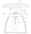
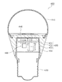
グローブ10の中空の内部空間(以下「中空空間」という)には、その上部に充填部材90が配置される。つまり、充填部材90は、グローブ10の中空空間上部を充填する部材である。充填部材90は、上側の曲面全体がグローブ10の内面と接しており、下側の平面が中空空間に開放されている。そして、充填部材90の下側の平面の中央には、LEDモジュール20の上部が嵌合する凹部91が形成されている。このため、充填部材90は、LEDモジュールを挟んで口金30とは反対側において、グローブ10と基板21とを熱的に接続することになる。凹部91は、液状状態の充填部材90がグローブ10の中空空間に充填された後に、LEDモジュール20の基板21(後述参照)の上部を差し込んだ結果として形成される。つまり、凹部91は、LEDモジュール20の基板21(後述参照)の水平方向における断面の矩形と同じ形状とすることができる。なお、凹部91は、液状状態の充填部材90に基板21を挿し込むことにより形成する他に、予め凹部91を有する充填部材90を成形しておいても良く、基板21は、後から充填部材90の凹部91に挿し込んで固定するようにしてもよい。基板21は、その下側の短辺側の端縁部(第1固定領域FA1の一部又は全部)が当該凹部91に差し込まれることにより、充填部材90に固定されている。なお、充填部材90と基板21とは、凹部91周辺に塗布された接着剤等によって固着されている。また、充填部材90は、口金30と基板21との延長線上にある範囲を少なくとも含むグローブ10の内面と熱的に接続するようにすることが好ましい。   In the hollow internal space of the globe 10 (hereinafter referred to as “hollow space”), a filling member 90 is disposed on the top thereof. That is, the filling member 90 is a member that fills the upper part of the hollow space of the globe 10. The entire upper curved surface of the filling member 90 is in contact with the inner surface of the globe 10, and the lower plane is open to the hollow space. A recess 91 into which the upper part of the LED module 20 is fitted is formed in the center of the lower plane of the filling member 90. For this reason, the filling member 90 thermally connects the globe 10 and the substrate 21 on the side opposite to the base 30 with the LED module interposed therebetween. The recess 91 is formed as a result of inserting the upper portion of the substrate 21 (see later) of the LED module 20 after the filling member 90 in the liquid state is filled in the hollow space of the globe 10. That is, the recessed part 91 can be made into the same shape as the rectangle of the cross section in the horizontal direction of the board | substrate 21 (refer later) of the LED module 20. In addition to forming the recess 91 by inserting the substrate 21 into the filling member 90 in a liquid state, the filling member 90 having the recess 91 may be formed in advance. You may make it insert in the recessed part 91 of 90, and you may make it fix. The substrate 21 is fixed to the filling member 90 by inserting an end portion (a part or all of the first fixing area FA1) on the short side below the substrate 21 into the recess 91. The filling member 90 and the substrate 21 are fixed by an adhesive applied around the recess 91. Further, it is preferable that the filling member 90 is thermally connected to the inner surface of the globe 10 including at least a range on the extension line between the base 30 and the substrate 21.

このように、充填部材90はLEDモジュール20の基板21とグローブ10とを接続しているため、LEDモジュール20の熱は、充填部材90を介してグローブ10に熱伝導し、グローブの外表面から大気中に放熱される。   Thus, since the filling member 90 connects the substrate 21 of the LED module 20 and the globe 10, the heat of the LED module 20 is thermally conducted to the globe 10 through the filling member 90, and from the outer surface of the globe. Heat is released to the atmosphere.

また、充填部材90は、透光性を有しており、透過率が95%の透光性材料で構成されている。このように、充填部材90は透光性を有する材料であるため、グローブ内に配置されたLEDモジュール20は、グローブ10の上側から視認することができる。グローブ10と同様に、充填部材90を透明とすることにより、LEDモジュール20からの光が充填部材90によって損失することを抑制することができる。また、充填部材90は、グローブ10と同様に、透明でなくてもよく、充填部材90の下側の平面に拡散膜を形成する等の拡散処理を施しても構わない。なお、充填部材90の下側に形成される面は平面に限らずに、曲面であってもよい。   The filling member 90 is translucent and is made of a translucent material having a transmittance of 95%. Thus, since the filling member 90 is a material having translucency, the LED module 20 disposed in the globe can be viewed from the upper side of the globe 10. Similarly to the globe 10, by making the filling member 90 transparent, it is possible to prevent the light from the LED module 20 from being lost by the filling member 90. Further, like the globe 10, the filling member 90 may not be transparent, and may be subjected to a diffusion treatment such as forming a diffusion film on the lower plane of the filling member 90. The surface formed below the filling member 90 is not limited to a flat surface, and may be a curved surface.

また、充填部材90は、熱硬化性の透明シリコーン樹脂であり、熱伝導率が0.17[W/m・K]である。なお、充填部材90は、熱可塑性の透明樹脂であってもよい。なお、充填部材90が熱硬化性の透明樹脂の場合には、例えば、LEDモジュール20を発光させた際の、発熱を利用して透明樹脂を硬化させるようにしてもよい。また、充填部材90は、ガラスの熱伝導率よりも大きい熱伝導率の材料で構成することが好ましく、例えば、熱伝導フィラー(金属微粒子を含む)を透明樹脂に添加することにより熱伝導性を大きくすることが好ましい。   The filling member 90 is a thermosetting transparent silicone resin and has a thermal conductivity of 0.17 [W / m · K]. The filling member 90 may be a thermoplastic transparent resin. In the case where the filling member 90 is a thermosetting transparent resin, for example, the transparent resin may be cured using heat generated when the LED module 20 emits light. The filling member 90 is preferably made of a material having a thermal conductivity larger than that of glass. For example, a thermal conductive filler (including metal fine particles) is added to the transparent resin to increase the thermal conductivity. It is preferable to enlarge it.

なお、本実施形態では、充填部材90に凹部91を形成して、基板21と充填部材90とを固定したが、必ずしも凹部91を形成する必要はない。例えば、充填部材90の下面の平面に基板21の側面を当接させるようにして基板21を縦向きに配置して固着しても構わない。また、本実施形態では、充填部材90と基板21とは接着剤で固着したが、これに限らない。例えば、ねじ等によって充填部材90と基板21とを固定しても構わない。   In the present embodiment, the recess 91 is formed in the filling member 90 and the substrate 21 and the filling member 90 are fixed. However, the recess 91 is not necessarily formed. For example, the substrate 21 may be arranged vertically and fixed so that the side surface of the substrate 21 is in contact with the plane of the lower surface of the filling member 90. Moreover, in this embodiment, although the filling member 90 and the board | substrate 21 adhered with the adhesive agent, it is not restricted to this. For example, the filling member 90 and the substrate 21 may be fixed by screws or the like.

次に、LEDモジュール20について説明する。LEDモジュール20は、所定の光を発光する発光モジュール(発光装置)であって、グローブ10内に収納されている。LEDモジュール20は、その上部が充填部材90によって支持固定され、その下部が固定部材40によって支持固定されており、好ましくは、LEDモジュール20の発光部がグローブ10の中心位置(例えば、グローブ10の内径が大きい径大部分の内部)に配置される。このように配置することにより、電球形ランプ1は、点灯時に従来のフィラメントコイルを用いた一般白熱電球と近似した配光特性を得ることができる。なお、LEDモジュール20は、2本の第1のリード線71及び第2のリード線72から電力が供給されることにより発光する。これら、リード線は、一般的に用いられる被覆線を用いたが、Ni−Fe線等他の導線を用いてもよい。   Next, the LED module 20 will be described. The LED module 20 is a light emitting module (light emitting device) that emits predetermined light, and is housed in the globe 10. The LED module 20 has an upper portion supported and fixed by a filling member 90 and a lower portion supported and fixed by a fixing member 40. Preferably, the light emitting portion of the LED module 20 is positioned at the center position of the globe 10 (for example, the globe 10). The inside of the large diameter part with a large inside diameter) is arranged. By arranging in this way, the light bulb shaped lamp 1 can obtain a light distribution characteristic approximate to that of a general incandescent light bulb using a conventional filament coil at the time of lighting. The LED module 20 emits light when power is supplied from the two first lead wires 71 and the second lead wire 72. As these lead wires, generally used coated wires are used, but other conductive wires such as Ni-Fe wires may be used.

ここで、本実施形態に係るLEDモジュール20の各構成要素について、図4を用いてさらに詳述する。図4(a)は、本発明の第1の実施形態に係る電球形ランプにおけるLEDモジュールの平面図(第1の主面側の平面図)であり、図4(b)は、同LEDモジュールの背面図(第2の主面側の平面図)であり、図4(c)は、図4(a)のA−A’線に沿って切断した同LEDモジュールの断面図である。   Here, each component of the LED module 20 which concerns on this embodiment is further explained in full detail using FIG. Fig.4 (a) is a top view (plan view of the 1st main surface side) of the LED module in the lightbulb-shaped lamp which concerns on the 1st Embodiment of this invention, FIG.4 (b) is the LED module FIG. 4C is a cross-sectional view of the LED module cut along the line AA ′ of FIG. 4A.

図4(a)〜図4(c)に示すように、本実施形態に係るLEDモジュール20は、透
光性の基板21と、発光源であるLED22と、LED22を封止するための封止部材23と、配線24と、ワイヤー25とを備える。さらに、LEDモジュール20は、波長変換部材として機能する蛍光体層26と、第1の給電端子27と、第2の給電端子28とを備える。
As shown in FIG. 4A to FIG. 4C, the LED module 20 according to this embodiment includes a light-transmitting substrate 21, an LED 22 that is a light emitting source, and a seal for sealing the LED 22. The member 23, the wiring 24, and the wire 25 are provided. Furthermore, the LED module 20 includes a phosphor layer 26 that functions as a wavelength conversion member, a first power supply terminal 27, and a second power supply terminal 28.

なお、本実施形態に係るLEDモジュール20は、基板21上にLEDチップ(ベアチップ)が直接実装されて構成されるCOB型(Chip On Board)のLEDモジュールである。   The LED module 20 according to the present embodiment is a COB type (Chip On Board) LED module configured by directly mounting an LED chip (bare chip) on a substrate 21.

まず、基板21について説明する。基板21は、LED22が実装される平面を構成する第1の主面21aと、当該第1の主面21aとは反対側の平面を構成する第2の主面21bとを有する長尺矩形状の板状基板であって、LED22が発する光を透光する透光性基板である。   First, the substrate 21 will be described. The substrate 21 has a long rectangular shape having a first main surface 21a constituting a plane on which the LEDs 22 are mounted and a second main surface 21b constituting a plane opposite to the first main surface 21a. This is a translucent substrate that transmits light emitted from the LEDs 22.

また、本実施形態において、LEDモジュール20は、基板21の両主面から光を放出するように構成されており、図4(a)に示すように、基板21は、LED22による所定の光が第1の主面21aからグローブ10に向かって放出される領域である第1の光放出領域LA1と、LED22による所定の光が第2の主面21bからグローブ10に向かって放出される領域である第2の光放出領域LA2とを有する。第1の光放出領域LA1及び第2の光放出領域LA2は、LEDモジュール20における発光部として機能し、放射強度が高く、高光度の領域である。なお、本実施形態では、第1の光放出領域LA1及び第2の光放出領域LA2からは、後述するように、所定の光としてLED22の光が波長変換された光が放出される。   In the present embodiment, the LED module 20 is configured to emit light from both main surfaces of the substrate 21. As shown in FIG. 4A, the substrate 21 receives predetermined light from the LEDs 22. A first light emission region LA1 that is a region emitted from the first main surface 21a toward the globe 10 and a region in which predetermined light from the LED 22 is emitted from the second main surface 21b toward the globe 10. A second light emission region LA2. The first light emission area LA1 and the second light emission area LA2 function as a light emitting part in the LED module 20, have high radiation intensity, and are areas with high luminous intensity. In the present embodiment, as described later, light obtained by wavelength-converting the light of the LED 22 is emitted from the first light emission area LA1 and the second light emission area LA2.

さらに、本実施形態において、LEDモジュール20は、LED22が片面のみに実装された構成となっており、第1の主面21aに実装されたLED22の光が、基板21の内部を透過してLED22が実装されていない第2の主面21bからも放出され、これにより、基板21の両主面から光が放出される。   Further, in the present embodiment, the LED module 20 has a configuration in which the LED 22 is mounted only on one side, and the light of the LED 22 mounted on the first main surface 21a is transmitted through the inside of the substrate 21 and the LED 22. Is also emitted from the second main surface 21b where the substrate is not mounted, whereby light is emitted from both main surfaces of the substrate 21.

このため、基板21は、可視光に対する透過率が80%以上の材料で構成することが好ましく、可視光領域の光に対して透明、すなわち、透過率が極めて高く向こう側が透けて見える状態の材料で構成することがより好ましい。これにより、LED22が基板21の一方の面(第1の主面)だけに実装された場合であっても、他方の面(第2の主面)からも光が容易に放出されるので、白熱電球と近似した全方位配光特性を得ることが可能となる。   For this reason, the substrate 21 is preferably made of a material having a transmittance of 80% or more for visible light, and is transparent to light in the visible light region, that is, a material in which the transmittance is extremely high and the other side can be seen through. More preferably, Thereby, even when the LED 22 is mounted only on one surface (first main surface) of the substrate 21, light is easily emitted from the other surface (second main surface). An omnidirectional light distribution characteristic similar to that of an incandescent bulb can be obtained.

このような基板21としては、アルミナや窒化アルミニウムからなる透光性セラミックス基板、透明なガラス基板、水晶からなる基板又はサファイア基板等を用いることができる。本実施形態では、基板21として、放熱性も考慮して、透過率が96%であるアルミナからなる透光性のセラミックス基板(アルミナ基板)を用いた。また、基板21の寸法としては、長さ22mm、幅18mm、厚さ1.0mmの矩形状の基板とした。   As such a substrate 21, a translucent ceramic substrate made of alumina or aluminum nitride, a transparent glass substrate, a substrate made of quartz, a sapphire substrate, or the like can be used. In the present embodiment, a light-transmitting ceramic substrate (alumina substrate) made of alumina having a transmittance of 96% is used as the substrate 21 in consideration of heat dissipation. The dimensions of the substrate 21 were a rectangular substrate having a length of 22 mm, a width of 18 mm, and a thickness of 1.0 mm.

また、基板21は、図4(a)に示すように、充填部材90に固定される領域である第1固定領域FA1と、固定部材40に固定される領域である第2固定領域FA2とを有する。つまり、基板21は、一端が充填部材90に接続され、他端が固定部材40に立設されて固定される。第1固定領域FA1及び第2固定領域FA2は、第1の光放出領域LA1及び第2の光放出領域LA2とは異なる領域であって、基本的にはLEDモジュール20の発光部としては機能しない領域である。すなわち、LED22による光が基板21内を伝達して第1固定領域FA1及び第2固定領域FA2から放出することがあったとしても放射強度が低く、第1固定領域FA1及び第2固定領域FA2は低光度の領域である。本実施形態において、第1固定領域FA1及び第2固定領域FA2は、基板21の長手方向の両方の端縁部で構成されている。第1固定領域FA1及び第2固定領域FA2としての端縁部は、少なくとも、基板21の短辺側の側面を含み、本実施形態では、第1の主面21a及び第2の主面21bをも含む。なお、当該端縁部には、基本的には基板保護層及び絶縁層以外は何も形成されておらず、例えば、LED22、封止部材23、配線24、ワイヤー25、蛍光体層26、第1の給電端子27及び第2の給電端子28は形成されていない。   As shown in FIG. 4A, the substrate 21 includes a first fixed area FA1 that is an area fixed to the filling member 90 and a second fixed area FA2 that is an area fixed to the fixing member 40. Have. That is, one end of the substrate 21 is connected to the filling member 90, and the other end is erected and fixed to the fixing member 40. The first fixed area FA1 and the second fixed area FA2 are areas different from the first light emitting area LA1 and the second light emitting area LA2, and basically do not function as the light emitting part of the LED module 20. It is an area. That is, even if light from the LED 22 is transmitted through the substrate 21 and emitted from the first fixed area FA1 and the second fixed area FA2, the radiation intensity is low, and the first fixed area FA1 and the second fixed area FA2 This is a low light intensity region. In the present embodiment, the first fixed area FA1 and the second fixed area FA2 are configured by both edge portions of the substrate 21 in the longitudinal direction. The edge portions as the first fixed area FA1 and the second fixed area FA2 include at least the side surface on the short side of the substrate 21, and in the present embodiment, the first main surface 21a and the second main surface 21b are provided. Including. Note that nothing is formed on the edge portion except for the substrate protective layer and the insulating layer. For example, the LED 22, the sealing member 23, the wiring 24, the wire 25, the phosphor layer 26, the second layer The first power supply terminal 27 and the second power supply terminal 28 are not formed.

次に、LED22について説明する。LED22は、半導体発光素子の一例であって、基板21の第1の主面21a上に直接実装されている。本実施形態において、LED22は、単色の可視光を発するベアチップであり、基板21上に複数個実装されている。各LED22は、全方位、つまり上方、側方及び下方に向けて光を発し、例えば、上方(第1の主面から基板外部に向かう方向)に全光量の60%、側方(基板水平方向)に全光量の20%、下方(第1の主面から第2の主面に向かう方向)に全光量の20%の光を発する。なお、LED22は、ダイアタッチ剤(ダイボンド剤)によって基板21上にダイボンディングされている。   Next, the LED 22 will be described. The LED 22 is an example of a semiconductor light emitting element, and is directly mounted on the first main surface 21 a of the substrate 21. In this embodiment, the LEDs 22 are bare chips that emit monochromatic visible light, and a plurality of LEDs 22 are mounted on the substrate 21. Each LED 22 emits light in all directions, that is, upward, sideward, and downward. For example, 60% of the total amount of light is upward (in the direction from the first main surface toward the outside of the substrate), and laterally (in the substrate horizontal direction). ) 20% of the total light quantity, and 20% of the total light quantity is emitted downward (in the direction from the first main surface to the second main surface). The LED 22 is die-bonded on the substrate 21 with a die attach agent (die bond agent).

本実施形態において、LED22は、例えば、通電されれば青色光を発光する青色LEDチップが用いられる。青色LEDチップとしては、例えばInGaN系の材料によって構成された、中心波長が440nm〜470nmの窒化ガリウム系の半導体発光素子を用いることができる。また、本実施形態において、LED22は、基板21の第1の主面21aのみの片面にのみ実装されており、9個のLED22を一列として直線状に2列配置し、列内のLED22は直列接続となるように、列同士のLED22は並列接続となるように電気的に接続されている。   In the present embodiment, for example, a blue LED chip that emits blue light when energized is used as the LED 22. As the blue LED chip, for example, a gallium nitride based semiconductor light emitting device having a center wavelength of 440 nm to 470 nm, which is made of an InGaN based material, can be used. In the present embodiment, the LEDs 22 are mounted only on one side of the first main surface 21a of the substrate 21. The nine LEDs 22 are arranged in a straight line in two rows, and the LEDs 22 in the row are in series. The LEDs 22 in the rows are electrically connected so as to be connected in parallel so as to be connected.

なお、LED22の個数及び配列は、電球形ランプの用途に応じて適宜、変更されればよい。例えば、豆電球やなつめ球の代替用途においては、基板21上に実装されるLED22は1個であってもよい。また、複数個のLED22は、1列で実装してもよく、あるいは、2列以外の複数列で実装しても構わない。   Note that the number and arrangement of the LEDs 22 may be appropriately changed according to the use of the light bulb shaped lamp. For example, in an alternative application of a miniature light bulb or a ball ball, the number of LEDs 22 mounted on the substrate 21 may be one. Further, the plurality of LEDs 22 may be mounted in one row, or may be mounted in a plurality of rows other than two rows.

次に、封止部材23について説明する。封止部材23は、LED22を封止するようにして基板21の第1の主面21a上に形成されている。本実施形態において、封止部材23は、複数のLED22を、LED22の列ごとに一括封止するように形成されており、図4(a)に示すように、直線状の2列で構成されている。   Next, the sealing member 23 will be described. The sealing member 23 is formed on the first main surface 21 a of the substrate 21 so as to seal the LED 22. In the present embodiment, the sealing member 23 is formed so as to collectively seal a plurality of LEDs 22 for each row of the LEDs 22, and is configured by two linear rows as shown in FIG. ing.

また、封止部材23は、LED22が発する光の波長を変換する第1の波長変換材を有する。封止部材23は、所定の樹脂の中に第1の波長変換材として所定の蛍光体粒子が含有された蛍光体含有樹脂を用いることができ、例えば、シリコーン樹脂等の透光性樹脂材料に蛍光体粒子を分散することによって構成することができる。   Further, the sealing member 23 includes a first wavelength conversion material that converts the wavelength of light emitted from the LED 22. The sealing member 23 can use a phosphor-containing resin in which predetermined phosphor particles are contained as a first wavelength conversion material in a predetermined resin. For example, a light-transmitting resin material such as a silicone resin can be used. It can be configured by dispersing phosphor particles.

このように、本実施形態において、封止部材23は、LED22が発する光を、ランプの照明光である所定の光として波長変換する第1の波長変換部であるとともに、LEDモジュール20における基板21の第1の主面側の発光部(第1の発光部)である。なお、上述の第1の光放出領域LA1は、封止部材23が形成される領域を含む領域であって、所定の光を放出するように見える高光度領域である。   Thus, in this embodiment, the sealing member 23 is a first wavelength conversion unit that converts the wavelength of light emitted from the LED 22 as predetermined light that is illumination light of the lamp, and the substrate 21 in the LED module 20. It is the light emission part (1st light emission part) of the 1st main surface side. The first light emission region LA1 described above is a region including a region where the sealing member 23 is formed, and is a high light intensity region that appears to emit predetermined light.

具体的に、封止部材23としては、例えばLED22が青色LEDである場合であって、ランプの照明光が白色光である場合は、YAG(イットリウム・アルミニウム・ガーネット)系の黄色蛍光体粒子をシリコーン樹脂に分散させた蛍光体含有樹脂を用いることができる。これにより、LED22が発した青色光の一部は、封止部材23に含まれる黄色蛍光体粒子によって黄色光に波長変換される。そして、黄色蛍光体粒子に吸収されなかった青色光と、黄色蛍光体粒子によって波長変換された黄色光とが、封止部材23の中で拡散し、混合されることにより、封止部材23から白色光となって外部に放出される。   Specifically, as the sealing member 23, for example, when the LED 22 is a blue LED and the illumination light of the lamp is white light, YAG (yttrium, aluminum, garnet) -based yellow phosphor particles are used. A phosphor-containing resin dispersed in a silicone resin can be used. Thereby, a part of the blue light emitted from the LED 22 is converted into yellow light by the yellow phosphor particles contained in the sealing member 23. Then, the blue light that has not been absorbed by the yellow phosphor particles and the yellow light that has been wavelength-converted by the yellow phosphor particles are diffused and mixed in the sealing member 23, so that the sealing member 23 White light is emitted to the outside.

このように構成される封止部材23は、例えば、以下のような2つの工程を経て形成される。まず、第1工程では、波長変換材(蛍光体粒子)を含む未硬化のペースト状の封止部材23の材料を、ディスペンサーによって複数のLED22を覆うようにして基板21の第1の主面21a上に直線状に塗布する。次に、第2工程では、塗布されたペースト状の封止部材23の材料を硬化させる。これにより、封止部材23を形成することができ、形成された封止部材23の断面形状は、ドーム状であって、幅1mm、高さ0.2mmである。   The sealing member 23 configured as described above is formed, for example, through the following two steps. First, in the first step, the material of the uncured pasty sealing member 23 containing the wavelength conversion material (phosphor particles) is covered with a first main surface 21a of the substrate 21 so as to cover the plurality of LEDs 22 with a dispenser. Apply linearly on top. Next, in the second step, the applied paste-like sealing member 23 is cured. Thereby, the sealing member 23 can be formed, and the cross-sectional shape of the formed sealing member 23 is a dome shape with a width of 1 mm and a height of 0.2 mm.

なお、本実施形態では、封止部材23に含有される第1の波長変換材としては、YAG系の黄色蛍光体粒子を用いたが、これに限らない。例えば、その他の黄色蛍光体粒子であってもよいし、あるいは、黄色蛍光体粒子に代えて緑色蛍光体粒子と赤色蛍光体粒子とを用いても構わない。   In the present embodiment, YAG-based yellow phosphor particles are used as the first wavelength conversion material contained in the sealing member 23, but the present invention is not limited to this. For example, other yellow phosphor particles may be used, or green phosphor particles and red phosphor particles may be used in place of the yellow phosphor particles.

また、封止部材23の主材料は、必ずしもシリコーン樹脂である必要はなく、フッ素系樹脂などの有機材料を用いてもよいし、低融点ガラスやゾルゲルガラス等の無機材料を用いてもよい。なお、無機材料は有機材料に比べて耐熱特性が優れているので、無機材料からなる封止部材23は高輝度ランプに有利である。   Moreover, the main material of the sealing member 23 does not necessarily need to be a silicone resin, Organic materials, such as a fluorine resin, may be used, and inorganic materials, such as low melting glass and sol-gel glass, may be used. In addition, since the inorganic material has better heat resistance characteristics than the organic material, the sealing member 23 made of the inorganic material is advantageous for a high-intensity lamp.

さらに、封止部材23には、必要に応じて適宜光拡散材を含有させてもよい。光拡散材としては、シリカなどの粒子が用いられる。   Furthermore, the sealing member 23 may contain a light diffusing material as needed. As the light diffusing material, particles such as silica are used.

また、本実施形態において、封止部材23は、LED22の列ごとに形成したが、実装された全てのLED22を一括封止するように形成しても構わない。   Moreover, in this embodiment, although the sealing member 23 was formed for every row | line | column of LED22, you may form so that all mounted LED22 may be sealed collectively.

次に、配線24について説明する。配線24は、導電部材によって構成されており、複数のLED22同士を電気的に接続するために、基板21の第1の主面21aに所定形状でパターン形成されている。本実施形態において、配線24は、列内の9個のLED22が直列接続となるように、また、列同士のLED22が並列接続となるように、パターン形成されている。   Next, the wiring 24 will be described. The wiring 24 is composed of a conductive member, and is patterned in a predetermined shape on the first main surface 21a of the substrate 21 in order to electrically connect the plurality of LEDs 22 to each other. In this embodiment, the wiring 24 is patterned so that the nine LEDs 22 in the row are connected in series, and the LEDs 22 in the rows are connected in parallel.

また、配線24は、第1の給電端子27と一方の端部側のLED22とを電気的に接続するとともに、第2の給電端子28と他方の端部側のLED22とを電気的に接続するためにも形成されている。   The wiring 24 electrically connects the first power supply terminal 27 and the LED 22 on one end side, and electrically connects the second power supply terminal 28 and the LED 22 on the other end side. Also formed for.

配線24は、例えば、銀(Ag)、タングステン(W)又は銅(Cu)等の金属配線を用いることができ、その表面にはニッケル(Ni)/金(Au)等のメッキ処理が施されている。なお、配線24は、ITO(Indium Tin Oxide)等の透光性導電部材により形成してもよい。   For the wiring 24, for example, a metal wiring such as silver (Ag), tungsten (W), or copper (Cu) can be used, and the surface thereof is plated with nickel (Ni) / gold (Au) or the like. ing. The wiring 24 may be formed of a light-transmitting conductive member such as ITO (Indium Tin Oxide).

次に、ワイヤー25について説明する。ワイヤー25は、LED22と配線24とを電気的に接続するための電線であり、例えば、金ワイヤーで構成される。LED22のチップ上面には電流を供給するためのp側電極及びn側電極が形成されており、p側電極及びn側電極と配線24とがワイヤー25によってワイヤボンディングされている。なお、本実施形態において、ワイヤー25は、封止部材23に埋め込まれるようにして構成されている。   Next, the wire 25 will be described. The wire 25 is an electric wire for electrically connecting the LED 22 and the wiring 24, and is composed of, for example, a gold wire. A p-side electrode and an n-side electrode for supplying current are formed on the upper surface of the chip of the LED 22, and the p-side electrode and the n-side electrode and the wiring 24 are wire-bonded by a wire 25. In the present embodiment, the wire 25 is configured to be embedded in the sealing member 23.

次に、蛍光体層26について説明する。図4(b)及び図4(c)に示すように、蛍光体層26は、基板21の第1の主面21aにパターン形成された薄膜状の焼結体であって、基板21を透光したLED22の光の波長を変換する第2の波長変換材と、無機材料からなる焼結用結合材とで構成されている。蛍光体層26は、基板21とLED22との間にパターン形成される。   Next, the phosphor layer 26 will be described. As shown in FIGS. 4B and 4C, the phosphor layer 26 is a thin film-like sintered body patterned on the first main surface 21 a of the substrate 21, and passes through the substrate 21. It is comprised by the 2nd wavelength conversion material which converts the wavelength of the light of lighted LED22, and the binder for sintering which consists of inorganic materials. The phosphor layer 26 is patterned between the substrate 21 and the LED 22.

蛍光体層26の第2の波長変換材は、基板21の第1の主面21aに実装されたLED22が発する光のうち基板21を透光した光の波長を変換して波長変換光を放射する。第2の波長変換材としては、LED22が発する光によって励起されて所望の光を放出する蛍光体粒子を用いることができる。例えば、LED22が青色光を発する青色LEDである場合であってランプの照明光として白色光を得る場合は、上述の封止部材23における第1の波長変換材と同様に、YAG系の黄色蛍光体粒子等を用いることができる。   The second wavelength conversion material of the phosphor layer 26 radiates wavelength-converted light by converting the wavelength of light transmitted through the substrate 21 out of the light emitted from the LED 22 mounted on the first main surface 21a of the substrate 21. To do. As the second wavelength conversion material, phosphor particles that are excited by light emitted from the LED 22 and emit desired light can be used. For example, when the LED 22 is a blue LED that emits blue light and white light is obtained as the illumination light of the lamp, a YAG-based yellow fluorescent light is used similarly to the first wavelength conversion material in the sealing member 23 described above. Body particles and the like can be used.

蛍光体層26の焼結用結合材は、無機材料で構成されるとともに、LED22が発する光と第2の波長変換材によって波長変換されたLED22の光の波長変換光とを透光する。焼結用結合材としては、酸化シリコン(SiO2)を主成分とする材料で構成されるガラスフリット(フリットガラス)を用いることができる。ガラスフリットは、第2の波長変換材(蛍光体粒子)を基板21に結着させる結合材(結着材)であり、透過率が高い材料で構成されている。また、ガラスフリットは、ガラス粉末を加熱して溶解することによって形成することができる。ガラスフリットのガラス粉末としては、SiO2−B2O3−R2O系、B2O3−R2O系又はP2O5−R2O系(但し、R2Oは、いずれも、Li2O、Na2O、又は、K2Oである)を用いることができる。また、焼結用結合材の材料としては、ガラスフリット以外に、低融点結晶からなるSnO2−B2O3等を用いることもできる。   The binder for sintering the phosphor layer 26 is made of an inorganic material, and transmits light emitted from the LED 22 and wavelength converted light of the LED 22 converted in wavelength by the second wavelength converting material. As the binder for sintering, glass frit (frit glass) made of a material mainly composed of silicon oxide (SiO 2) can be used. The glass frit is a binding material (binding material) that binds the second wavelength conversion material (phosphor particles) to the substrate 21 and is made of a material having high transmittance. The glass frit can be formed by heating and melting glass powder. As the glass powder of the glass frit, SiO 2 —B 2 O 3 —R 2 O, B 2 O 3 —R 2 O, or P 2 O 5 —R 2 O (wherein R 2 O is Li 2 O, Na 2 O, or K 2 O) can be used. In addition to glass frit, SnO2-B2O3 made of low-melting crystals can be used as a material for the binder for sintering.

このように構成される蛍光体層26は、第2の波長変換材、焼結用結合材、溶剤等を混錬することによって得られるペーストを、基板21の第1の主面21aに印刷又は塗布した後に焼結することによって形成することができる。   The phosphor layer 26 configured in this way prints or pastes the paste obtained by kneading the second wavelength conversion material, the binder for sintering, the solvent, etc. on the first main surface 21a of the substrate 21. It can be formed by applying and then sintering.

このように、本実施形態において、蛍光体層26は、LED22が発する光を、ランプの照明光である所定の光として波長変換する第2の波長変換部であるとともに、LEDモジュール20における基板21の第2の主面21b側に向けて発光する発光部(第2の発光部)である。なお、上述の第2の光放出領域LA2は、蛍光体層26が形成されている領域であって所定の光を放出するように見える高光度領域であり、本実施形態では、第1の光放出領域LA1と同じ面積の領域となるように構成されている。   Thus, in this embodiment, the phosphor layer 26 is a second wavelength conversion unit that converts the wavelength of light emitted from the LED 22 as predetermined light that is illumination light of the lamp, and the substrate 21 in the LED module 20. It is the light emission part (2nd light emission part) which light-emits toward the 2nd main surface 21b side. The second light emission region LA2 described above is a region where the phosphor layer 26 is formed and is a high light intensity region that appears to emit predetermined light. In the present embodiment, the first light emission region LA2 is the first light emission region LA2. The region is the same area as the emission region LA1.

また、本実施形態において、蛍光体層26は、膜厚が50μmの矩形状に形成されている。蛍光体層26の膜厚としては、10μm〜500μmであることが好ましい。   In the present embodiment, the phosphor layer 26 is formed in a rectangular shape with a film thickness of 50 μm. The film thickness of the phosphor layer 26 is preferably 10 μm to 500 μm.

なお、本実施形態では、第2の波長変換部として焼結体を用いたが、第2の波長変換部は、第1の波長変換部と同じ蛍光体含有樹脂によって構成することもできる。但し、第2の波長変換部を、無機材料からなる焼結体(蛍光体層26)によって構成することにより、樹脂で構成する場合と比べて、LED22の熱による劣化がないというだけではなく、LED22からの熱を効率良く放熱することも可能となる。これにより、高い信頼性と高い放熱特性を有するLEDモジュール20を実現することができる。   In the present embodiment, a sintered body is used as the second wavelength conversion unit. However, the second wavelength conversion unit can be formed of the same phosphor-containing resin as the first wavelength conversion unit. However, by configuring the second wavelength conversion section with a sintered body (phosphor layer 26) made of an inorganic material, not only is there no deterioration due to heat of the LED 22 compared to the case where it is configured with a resin, It is also possible to efficiently dissipate heat from the LED 22. Thereby, the LED module 20 having high reliability and high heat dissipation characteristics can be realized.

次に、第1の給電端子27及び第2の給電端子28について説明する。第1の給電端子27及び第2の給電端子28は、LED22を点灯させるための直流電圧を受電するためにLEDモジュール20外部の外部電源に接続するための接続端子であって、外部電源から受電した当該直流電圧をLED22に供給する給電端子である。本実施形態では、外部電源としてランプ内の点灯回路80から第1の給電端子27及び第2の給電端子28に対して直流電力が供給されることにより、配線24及びワイヤー25を介して各LED22に直流電力が供給される。これにより、LED22が発光(点灯)する。   Next, the first power supply terminal 27 and the second power supply terminal 28 will be described. The first power supply terminal 27 and the second power supply terminal 28 are connection terminals for connecting to an external power supply outside the LED module 20 in order to receive a DC voltage for lighting the LED 22, and receive power from the external power supply. This power supply terminal supplies the direct current voltage to the LED 22. In the present embodiment, the DC power is supplied from the lighting circuit 80 in the lamp to the first power supply terminal 27 and the second power supply terminal 28 as an external power source, whereby each LED 22 is connected via the wiring 24 and the wire 25. Is supplied with DC power. As a result, the LED 22 emits light (lights up).

図4(a)に示すように、本実施形態において、第1の給電端子27及び第2の給電端子28は、いずれも基板21の第1の主面21aに設けられており、第1の給電端子27と第2の給電端子28とは、基板21の長尺方向における一方の端部と他方の端部とに対向するようにして形成されている。なお、第1の給電端子27は、基板21における固定部材40側の端部に形成され、第2の給電端子28は、基板21における充填部材90側の端部に形成される。このように、第1の給電端子27と第2の給電端子28とを基板21の両端部に配置することにより、第1の給電端子27と第2の給電端子28との間の絶縁距離を確保することができるので、第1の給電端子27と第2の給電端子28との間で生じる放電等を防止することができる。   As shown in FIG. 4A, in the present embodiment, the first power supply terminal 27 and the second power supply terminal 28 are both provided on the first main surface 21a of the substrate 21, and The power supply terminal 27 and the second power supply terminal 28 are formed so as to face one end and the other end in the longitudinal direction of the substrate 21. The first power supply terminal 27 is formed at the end of the substrate 21 on the fixing member 40 side, and the second power supply terminal 28 is formed at the end of the substrate 21 on the filling member 90 side. In this way, by arranging the first power supply terminal 27 and the second power supply terminal 28 at both ends of the substrate 21, the insulation distance between the first power supply terminal 27 and the second power supply terminal 28 can be increased. Since it can be ensured, it is possible to prevent discharge or the like occurring between the first power supply terminal 27 and the second power supply terminal 28.

また、第1の給電端子27及び第2の給電端子28には、基板21を貫通する貫通孔27h及び28hが設けられている。貫通孔27h及び28hは、それぞれ第1のリード線71及び第2のリード線72の先端接続部分を挿入する箇所であって、図3に示すように、第1の給電端子27と第1のリード線71とを、また、第2の給電端子28を第2のリード線72とを、それぞれ半田102により電気的及び物理的に接続する接続部である。   Further, the first power supply terminal 27 and the second power supply terminal 28 are provided with through holes 27 h and 28 h penetrating the substrate 21. The through holes 27h and 28h are portions where the tip connecting portions of the first lead wire 71 and the second lead wire 72 are inserted, respectively, and as shown in FIG. The lead wire 71 and the second power supply terminal 28 are connected to the second lead wire 72 by a solder 102, respectively.

このように構成される本実施形態に係るLEDモジュール20は、上述のとおり放出する光は白色光に設定されており、基板21の第1の主面21a側における第1の発光部では、封止部材23内の黄色蛍光体粒子(第1の波長変換材)が青色LEDチップの青色光によって励起されて黄色光を放出し、第1の光放出領域LA1からは励起された黄色光と青色LEDチップの青色光とによって白色光が放出される。   In the LED module 20 according to this embodiment configured as described above, the light emitted is set to white light as described above, and the first light emitting unit on the first main surface 21a side of the substrate 21 is sealed. The yellow phosphor particles (first wavelength conversion material) in the stop member 23 are excited by the blue light of the blue LED chip to emit yellow light, and the excited yellow light and blue light are emitted from the first light emission region LA1. White light is emitted by the blue light of the LED chip.

一方、基板21の第2の主面21b側に向けて発光する第2発光部では、蛍光体層26内の黄色蛍光体粒子(第2の波長変換材)が基板21を透光した青色LEDチップの青色光によって励起されて黄色光を放出し、第2の光放出領域LA2からも白色光が放出される。   On the other hand, in the second light emitting unit that emits light toward the second main surface 21 b side of the substrate 21, the blue LED in which the yellow phosphor particles (second wavelength conversion material) in the phosphor layer 26 transmit the substrate 21. It is excited by the blue light of the chip to emit yellow light, and white light is also emitted from the second light emission region LA2.

そして、本実施形態に係るLEDモジュール20は、基板21が充填部材90及び固定部材40に支持されて充填部材90及び固定部材40に固定されている。すなわち、基板21は、立った状態で固定されており、少なくとも、第1の主面21aがグローブ10の開口部11の開口面と交差するようにして配置されている。   In the LED module 20 according to the present embodiment, the substrate 21 is supported by the filling member 90 and the fixing member 40 and is fixed to the filling member 90 and the fixing member 40. That is, the substrate 21 is fixed in a standing state, and is arranged so that at least the first main surface 21 a intersects the opening surface of the opening 11 of the globe 10.

本実施形態では、図1及び図3に示すように、基板21は、縦置き配置となるように充填部材90及び固定部材40に固定されており、第1の主面21aがグローブ10の開口部11の開口面のなす平面と略直交するようにして配置されている。すなわち、固定部材40と基板21と充填部材90との並び方向(つまり上下方向)に対して基板21の第1の主面21aが略平行となるようにLEDモジュール20は配置されている。   In this embodiment, as shown in FIGS. 1 and 3, the substrate 21 is fixed to the filling member 90 and the fixing member 40 so as to be vertically arranged, and the first main surface 21 a is an opening of the globe 10. It is arranged so as to be substantially orthogonal to the plane formed by the opening surface of the portion 11. That is, the LED module 20 is disposed so that the first main surface 21a of the substrate 21 is substantially parallel to the direction in which the fixing member 40, the substrate 21, and the filling member 90 are arranged (that is, the vertical direction).

この構成により、LEDモジュール20からの所定の光は、グローブ10の側周部方向に放出される。すなわち、第1の光放出領域LA1及び第2の光放出領域LA2からの所定の光は、グローブ10の側周部方向に放射状に放出する。これにより、LEDモジュール20をランプ光源とする全方位配光特性を実現することができる。なお、本実施形態では、第1の光放出領域LA1からの放出光と第2の光放出領域LA2からの放出光との光束は同程度となるように設定されている。   With this configuration, predetermined light from the LED module 20 is emitted in the direction of the side periphery of the globe 10. That is, the predetermined light from the first light emission region LA1 and the second light emission region LA2 is emitted radially toward the side circumferential portion of the globe 10. Thereby, the omnidirectional light distribution characteristic which makes the LED module 20 a lamp light source is realizable. In the present embodiment, the luminous fluxes of the emitted light from the first light emitting area LA1 and the emitted light from the second light emitting area LA2 are set to be approximately the same.

次に、口金30について説明する。図1〜図3に示すように、口金30は、LEDモジュール20のLED22を発光させるための電力を受電する受電部であって、本実施形態では、二接点によってランプ外部の交流電源(例えば、AC200Vの商用電源)から交流電圧を受電する。口金30で受電した電力はリード線を介して点灯回路80の電力入力部に入力される。口金30は、電球形ランプ1において1箇所のみに配置される。   Next, the base 30 will be described. As shown in FIGS. 1 to 3, the base 30 is a power receiving unit that receives power for causing the LEDs 22 of the LED module 20 to emit light, and in this embodiment, an AC power source (e.g. AC voltage is received from an AC200V commercial power source. The power received by the base 30 is input to the power input unit of the lighting circuit 80 via the lead wire. The base 30 is disposed at only one place in the light bulb shaped lamp 1.

口金30は、例えばE形であり、図3に示すように、その外周面には照明装置のソケットに螺合させるための螺合部が形成されている。また、口金30の内周面には、樹脂ケース60に螺合させるための螺合部が形成されている。なお、口金30は、金属性の有底筒体形状である。   The base 30 is, for example, E-shaped, and as shown in FIG. 3, a screwing portion for screwing into the socket of the lighting device is formed on the outer peripheral surface thereof. Further, a screwing portion for screwing into the resin case 60 is formed on the inner peripheral surface of the base 30. The base 30 has a metallic bottomed cylindrical shape.

本実施形態において、口金30はE26形の口金である。したがって、電球形ランプ1は、商用の交流電源に接続されたE26口金用ソケットに取り付けて使用される。なお、口金30は、必ずしもE26形の口金である必要はなく、E17形などの口金であってもよい。また、口金30は、必ずしもネジ込み形の口金である必要はなく、例えば差し込み形などネジ込み形とは異なる形状の口金であってもよい。   In the present embodiment, the base 30 is an E26 type base. Therefore, the light bulb shaped lamp 1 is used by being attached to a socket for E26 base connected to a commercial AC power source. The base 30 does not necessarily have to be an E26 type base, and may be an E17 type base. Further, the base 30 is not necessarily a screw-type base, and may be a base having a shape different from the screw-type, such as a plug-in type.

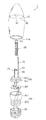
次に、固定部材40について説明する。図1〜図3に示すように、固定部材40は、LEDモジュール20をグローブ10内の所定の位置に固定するため部材であって、グローブ10の開口部11の近傍からグローブ10内に向かって延びるように構成されている。本実施形態において、固定部材40は、円柱形状であり、一端がLEDモジュール20に接続するように構成され、他端が支持部材50に接続されるように構成されている。   Next, the fixing member 40 will be described. As shown in FIGS. 1 to 3, the fixing member 40 is a member for fixing the LED module 20 to a predetermined position in the globe 10, and from the vicinity of the opening 11 of the globe 10 toward the inside of the globe 10. It is comprised so that it may extend. In the present embodiment, the fixing member 40 has a cylindrical shape, and is configured such that one end is connected to the LED module 20 and the other end is connected to the support member 50.

固定部材40の一端側の上面(LEDモジュール20側の面)には、溝部41が形成されている。溝部41は、溝幅がLEDモジュール20における基板21の板厚と同程度の長さとなるように構成されており、例えば、溝部41の形状は、基板21の端縁部と嵌合するような断面凹状の形状とすることができる。基板21は、その下側の短辺側の端縁部(第2固定領域FA2の一部又は全部)が当該溝部41に差し込まれることにより、固定部材40に固定されている。なお、固定部材40と基板21とは、溝部41周辺に塗布された接着剤等によって固着されている。   A groove portion 41 is formed on the upper surface (the surface on the LED module 20 side) on one end side of the fixing member 40. The groove portion 41 is configured such that the groove width is approximately the same as the plate thickness of the substrate 21 in the LED module 20. For example, the shape of the groove portion 41 is fitted to the edge portion of the substrate 21. The shape can be concave in cross section. The substrate 21 is fixed to the fixing member 40 by inserting an edge portion (a part or all of the second fixing area FA2) on the short side below the substrate 21 into the groove 41. Note that the fixing member 40 and the substrate 21 are fixed by an adhesive or the like applied around the groove 41.

このように、本実施形態において、LEDモジュール20は、基板21が固定部材40の溝部41に差し込まれることによって固定部材40に固定されている。これにより、基板21の位置や向き(LEDモジュール20の位置や向き)を溝部41によって規制することができるとともに、グローブ10内にLEDモジュール20を安定して配置固定することができる。   Thus, in the present embodiment, the LED module 20 is fixed to the fixing member 40 by inserting the substrate 21 into the groove 41 of the fixing member 40. Accordingly, the position and orientation of the substrate 21 (position and orientation of the LED module 20) can be regulated by the groove portion 41, and the LED module 20 can be stably disposed and fixed in the globe 10.

なお、本実施形態では、固定部材40に溝部41を形成して、基板21と固定部材40とを固定したが、必ずしも溝部41を形成する必要はない。例えば、固定部材40の上面の平面部分に基板21の側面を当接させるようにして基板21を縦向きに配置して固着しても構わない。また、本実施形態では、固定部材40と基板21とは接着剤で固着したが、これに限らない。例えば、ねじ等によって固定部材40と基板21とを固定しても構わない。   In this embodiment, the groove portion 41 is formed in the fixing member 40 and the substrate 21 and the fixing member 40 are fixed. However, the groove portion 41 is not necessarily formed. For example, the substrate 21 may be arranged vertically and fixed so that the side surface of the substrate 21 is brought into contact with the planar portion of the upper surface of the fixing member 40. In the present embodiment, the fixing member 40 and the substrate 21 are fixed with an adhesive, but the present invention is not limited to this. For example, the fixing member 40 and the substrate 21 may be fixed with screws or the like.

また、固定部材40の他端側(LEDモジュール20と固定する側とは反対側)の下面は支持部材50の表面に当接されており、固定部材40の下面と支持部材50とは当該当接部分において固定されている。本実施形態では、固定部材40と支持部材50とは、支持部材50の裏面からねじをねじ込むことによって固定されている。なお、固定部材40と支持部材50との固定方法は、ねじに限らず、接着剤等による固着によって固定しても構わない。   Further, the lower surface of the other end side of the fixing member 40 (the side opposite to the side fixed to the LED module 20) is in contact with the surface of the support member 50, and the lower surface of the fixing member 40 and the support member 50 are in contact with each other. It is fixed at the contact part. In the present embodiment, the fixing member 40 and the support member 50 are fixed by screwing screws from the back surface of the support member 50. The fixing method of the fixing member 40 and the support member 50 is not limited to screws, and may be fixed by fixing with an adhesive or the like.

さらに、固定部材40は、LEDモジュール20の基板21の熱伝導率よりも大きい熱伝導率の材料で構成されていることが好ましい。また、固定部材40は、ガラスの熱伝導率(1.0[W/m・K]程度)よりも大きい熱伝導率の材料で構成することが好ましく、例えば、金属材料又はセラミックス等の無機材料によって構成することができる。本実施形態において、固定部材40は、熱伝導率が237[W/m・K]であるアルミニウムで構成した。   Further, the fixing member 40 is preferably made of a material having a thermal conductivity larger than that of the substrate 21 of the LED module 20. The fixing member 40 is preferably made of a material having a thermal conductivity larger than that of glass (about 1.0 [W / m · K]). For example, a metal material or an inorganic material such as ceramics is used. Can be configured. In the present embodiment, the fixing member 40 is made of aluminum having a thermal conductivity of 237 [W / m · K].

このように、固定部材40の熱伝導率を基板21の熱伝導率よりも大きくすることにより、LEDモジュール20の熱は基板21を介して固定部材40に効率良く伝導する。これにより、LEDモジュール20の熱を口金30側に逃がすことができるので、温度上昇によるLED22の発光効率の低下及び寿命の低下を抑制することができる。   Thus, by making the thermal conductivity of the fixing member 40 larger than the thermal conductivity of the substrate 21, the heat of the LED module 20 is efficiently conducted to the fixing member 40 through the substrate 21. Thereby, since the heat | fever of the LED module 20 can be released to the nozzle | cap | die 30 side, the fall of the luminous efficiency of LED22 by the temperature rise and the fall of a lifetime can be suppressed.

次に、支持部材50について説明する。図2及び図3に示すように、支持部材50は、グローブ10の開口部11の開口端11aに接続され、固定部材40を支持する部材である。また、支持部材50は、グローブ10の開口部11を塞ぐように構成されている。本実施形態において、支持部材50は、樹脂ケース60に嵌合されて固定されている。また、支持部材50には、第1のリード線71及び第2のリード線72を挿通するための2つの挿通孔が形成されている。   Next, the support member 50 will be described. As shown in FIGS. 2 and 3, the support member 50 is a member that is connected to the opening end 11 a of the opening 11 of the globe 10 and supports the fixing member 40. The support member 50 is configured to close the opening 11 of the globe 10. In the present embodiment, the support member 50 is fitted and fixed to the resin case 60. The support member 50 is formed with two insertion holes for inserting the first lead wire 71 and the second lead wire 72.

支持部材50は、LEDモジュール20の基板21の熱伝導率よりも大きい熱伝導率の材料で構成することが好ましい。また、支持部材50は、ガラスの熱伝導率よりも大きい熱伝導率の材料で構成することが好ましく、例えば、金属材料又はセラミックス等の無機材料によって構成することができる。さらに、固定部材40の熱を支持部材50に効率良く伝導させるために、支持部材50の材料は、固定部材40の熱伝導率以上の熱伝導率の材料で構成することが好ましい。本実施形態において、支持部材50は、固定部材40と同じ材料によって、すなわち、熱伝導率が237[W/m・K]であるアルミニウムによって構成した。   The support member 50 is preferably made of a material having a thermal conductivity larger than that of the substrate 21 of the LED module 20. The support member 50 is preferably made of a material having a thermal conductivity larger than that of glass, and can be made of an inorganic material such as a metal material or ceramics. Furthermore, in order to efficiently conduct the heat of the fixing member 40 to the support member 50, the material of the support member 50 is preferably composed of a material having a thermal conductivity equal to or higher than the thermal conductivity of the fixing member 40. In the present embodiment, the support member 50 is made of the same material as that of the fixing member 40, that is, aluminum having a thermal conductivity of 237 [W / m · K].

このように、支持部材50を熱伝導率の大きい材料で構成することにより、固定部材40に熱伝導したLEDモジュール20の熱を支持部材50に効率良く伝導させることができるので、温度上昇によるLED22の発光効率の低下及び寿命の低下を抑制することができる。   In this way, by configuring the support member 50 with a material having a high thermal conductivity, the heat of the LED module 20 thermally conducted to the fixing member 40 can be efficiently conducted to the support member 50, and thus the LED 22 due to a temperature rise. It is possible to suppress a decrease in luminous efficiency and a decrease in lifetime.

また、本実施形態において、支持部材50は、円形の板状部材で構成され、第1支持部51と第2支持部52とからなる。支持部材50において、第2支持部52の直径は、第1支持部51の直径よりも大きくなるように構成されている。これにより、第1支持部51の周縁部と第2支持部52の周縁部との間には、段差部53が形成されている。なお、第1支持部51及び第2支持部52は一体成型されている。   In the present embodiment, the support member 50 is formed of a circular plate-shaped member and includes a first support portion 51 and a second support portion 52. In the support member 50, the diameter of the second support part 52 is configured to be larger than the diameter of the first support part 51. Thereby, a stepped portion 53 is formed between the peripheral edge portion of the first support portion 51 and the peripheral edge portion of the second support portion 52. In addition, the 1st support part 51 and the 2nd support part 52 are integrally molded.

図3に示すように、第1支持部51の上面(グローブ10側の面)には、固定部材40が固定されている。また、第2支持部52の側面には、樹脂ケース60の内面が当接している。段差部53には、グローブ10の開口部11の開口端11aが当接している。したがって、第2支持部52によってグローブ10の開口部11が塞がれている。また、段差部53において、支持部材50と樹脂ケース60とグローブ10の開口部11の開口端11aとは、接着材101によって固着されている。接着材101は、段差部53を埋めるようにして形成されている。   As shown in FIG. 3, the fixing member 40 is fixed to the upper surface (the surface on the globe 10 side) of the first support portion 51. Further, the inner surface of the resin case 60 is in contact with the side surface of the second support portion 52. The opening end 11 a of the opening 11 of the globe 10 is in contact with the stepped portion 53. Accordingly, the opening 11 of the globe 10 is blocked by the second support portion 52. Further, in the stepped portion 53, the support member 50, the resin case 60, and the opening end 11 a of the opening 11 of the globe 10 are fixed by the adhesive material 101. The adhesive material 101 is formed so as to fill the stepped portion 53.

このように、支持部材50がグローブ10に接続されているので、支持部材50に伝導したLEDモジュール20の熱は、外囲器を構成するグローブ10に熱伝導し、グローブ10の外表面から大気中に放熱される。   As described above, since the support member 50 is connected to the globe 10, the heat of the LED module 20 conducted to the support member 50 is conducted to the globe 10 constituting the envelope, and is transmitted from the outer surface of the globe 10 to the atmosphere. Heat is dissipated inside.

また、支持部材50は樹脂ケース60にも接続されているので、支持部材50に伝導したLEDモジュール20の熱は、樹脂ケース60に熱伝導し、外囲器を構成する樹脂ケース60の外表面からも大気中に放熱される。   Further, since the support member 50 is also connected to the resin case 60, the heat of the LED module 20 conducted to the support member 50 is conducted to the resin case 60, and the outer surface of the resin case 60 constituting the envelope. Heat is also released into the atmosphere.

なお、グローブ10等を固着する接着材101としては、例えば、シリコーン樹脂からなる接着剤を用いることができるが、LEDモジュール20の熱を支持部材50からグローブ10及び樹脂ケース60に効率良く伝導させるために、高熱伝導率の接着材を用いることが好ましい。例えば、シリコーン樹脂に金属微粒子を分散させること等によって熱伝導率を高くすることができる。   For example, an adhesive made of a silicone resin can be used as the adhesive 101 for fixing the globe 10 and the like, but the heat of the LED module 20 is efficiently conducted from the support member 50 to the globe 10 and the resin case 60. Therefore, it is preferable to use an adhesive having a high thermal conductivity. For example, the thermal conductivity can be increased by dispersing metal fine particles in a silicone resin.

次に、樹脂ケース60について説明する。図2及び図3に示すように、樹脂ケース60は、固定部材40と口金30とを絶縁するとともに点灯回路80を収納するための絶縁用のケースである。樹脂ケース60は、円筒状の第1ケース部61と、円筒状の第2ケース部62とからなる。   Next, the resin case 60 will be described. As shown in FIGS. 2 and 3, the resin case 60 is an insulating case for insulating the fixing member 40 and the base 30 and accommodating the lighting circuit 80. The resin case 60 includes a cylindrical first case portion 61 and a cylindrical second case portion 62.

第1ケース部61は、内径が支持部材50の第2支持部52の外径とほぼ同じであり、支持部材50は第1ケース部61に嵌合されて固定される。第1ケース部61の外表面は外気に露出しているので、樹脂ケース60に伝導した熱は、主に第1ケース部61から放熱される。   The first case portion 61 has an inner diameter that is substantially the same as the outer diameter of the second support portion 52 of the support member 50, and the support member 50 is fitted and fixed to the first case portion 61. Since the outer surface of the first case portion 61 is exposed to the outside air, the heat conducted to the resin case 60 is mainly radiated from the first case portion 61.

第2ケース部62は、外周面が口金30の内周面と接触するように構成されており、本実施形態では、第2ケース部62の外周面には口金30と螺合するための螺合部が形成されており、この螺合部によって第2ケース部62は口金30に接触している。したがって、樹脂ケース60に伝導した熱は、第2ケース部62を介して口金30にも伝導し、口金30の外表面からも放熱する。   The second case portion 62 is configured such that the outer peripheral surface is in contact with the inner peripheral surface of the base 30. In this embodiment, the second case portion 62 is screwed into the outer peripheral surface of the second case portion 62 to be screwed with the base 30. A joint portion is formed, and the second case portion 62 is in contact with the base 30 by this screwing portion. Therefore, the heat conducted to the resin case 60 is also conducted to the base 30 via the second case portion 62 and is radiated from the outer surface of the base 30.

本実施形態において、樹脂ケース60は、第1ケース部61と第2ケース部62とが一体的に形成されており、射出成形によって作製することができる。また、樹脂ケース60は、ガラス繊維を5〜15%含有してなる熱伝導率が0.35[W/m・K]のポリブチレンテレフタレート(PBT)によって成形されている。   In the present embodiment, the resin case 60 includes the first case portion 61 and the second case portion 62 that are integrally formed, and can be manufactured by injection molding. The resin case 60 is formed of polybutylene terephthalate (PBT) having a thermal conductivity of 0.35 [W / m · K] containing 5 to 15% of glass fiber.

次に、第1のリード線71及び第2のリード線72について説明する。図1〜図3に示すように、第1のリード線71及び第2のリード線72は、LEDモジュール20を発光させるための電力をLEDモジュール20に給電する電線であり、表面には絶縁性樹脂被膜がコーティングされている。   Next, the first lead wire 71 and the second lead wire 72 will be described. As shown in FIGS. 1-3, the 1st lead wire 71 and the 2nd lead wire 72 are electric wires which supply the electric power for making the LED module 20 light-emit to the LED module 20, and are insulated on the surface. Resin film is coated.

第1のリード線71及び第2のリード線72は、支持部材50を挿通して配置されており、第1のリード線71及び第2のリード線の一方側端はLEDモジュール20に接続されており、また、第1のリード線71及び第2のリード線72の他方側端は、点灯回路80の電力出力部に電気的に接続されている。   The first lead wire 71 and the second lead wire 72 are disposed through the support member 50, and one end of the first lead wire 71 and the second lead wire is connected to the LED module 20. The other end of the first lead wire 71 and the second lead wire 72 is electrically connected to the power output unit of the lighting circuit 80.

図3に示すように、第1のリード線71の一方側端の導電性の先端接続部分は、基板21の下端部における第1の給電端子27の貫通孔27hに挿入されており、第1のリード線71と第1の給電端子27とは半田102によって電気的に接続されている。   As shown in FIG. 3, the conductive tip connection portion at one end of the first lead wire 71 is inserted into the through hole 27 h of the first power supply terminal 27 at the lower end portion of the substrate 21. The lead wire 71 and the first power supply terminal 27 are electrically connected by solder 102.

また、第2のリード線72の一方側端の導電性の先端接続部分は、基板21の上端部にまで延設されて基板21の第2の給電端子28の貫通孔28hに挿入されており、第2のリード線72と第2の給電端子28とは半田102によって電気的に接続されている。   In addition, the conductive tip connecting portion at one end of the second lead wire 72 extends to the upper end portion of the substrate 21 and is inserted into the through hole 28 h of the second power supply terminal 28 of the substrate 21. The second lead wire 72 and the second power supply terminal 28 are electrically connected by the solder 102.

なお、基板21の上部にまで延設される第2のリード線72は、LEDモジュール20から放出される光を極力遮らないように、基板21の長辺側の側面に隣接させて当該側面に沿って配置することが好ましい。   The second lead wire 72 extending to the top of the substrate 21 is adjacent to the side surface on the long side of the substrate 21 so as not to block the light emitted from the LED module 20 as much as possible. It is preferable to arrange along.

次に、点灯回路80について説明する。図2及び図3に示すように、点灯回路80は、
LED22を点灯させるための回路であり、樹脂ケース60内に収納されている。点灯回路80は、複数の回路素子と、各回路素子を実装するための回路基板とを有する。
Next, the lighting circuit 80 will be described. As shown in FIGS. 2 and 3, the lighting circuit 80 includes:
This is a circuit for lighting the LED 22, and is housed in the resin case 60. The lighting circuit 80 includes a plurality of circuit elements and a circuit board for mounting each circuit element.

本実施形態において、点灯回路80は、口金30から受電した交流電力を直流電力に変換し、第1のリード線71及び第2のリード線72を介してLED22に当該直流電力を供給する。点灯回路80は、例えば、全波整流用のダイオードブリッジと、平滑用のコンデンサと、電流調整用の抵抗とによって構成することができる。   In the present embodiment, the lighting circuit 80 converts AC power received from the base 30 into DC power, and supplies the DC power to the LED 22 via the first lead wire 71 and the second lead wire 72. The lighting circuit 80 can be configured by, for example, a full-wave rectifying diode bridge, a smoothing capacitor, and a current adjusting resistor.

なお、電球形ランプ1は、必ずしも点灯回路80を内蔵する必要はない。例えば、照明器具あるいは電池などから直接直流電力が供給される場合には、電球形ランプ1は、点灯回路80を備えなくてもよい。また、点灯回路80は、平滑回路に限られるものではなく、調光回路、昇圧回路などを適宜選択、組み合わせることもできる。   The light bulb shaped lamp 1 does not necessarily need to incorporate the lighting circuit 80. For example, when direct-current power is directly supplied from a lighting fixture or a battery, the light bulb shaped lamp 1 may not include the lighting circuit 80. The lighting circuit 80 is not limited to a smoothing circuit, and a dimming circuit, a booster circuit, and the like can be appropriately selected and combined.

以上、本発明の第1の実施形態に係る電球形ランプ1によれば、LEDモジュール20において発生した熱を、点灯回路80が配置される固定部材40側から放熱させるだけでなく、その反対側の充填部材90側からグローブ10に伝導させて、グローブ10から放熱させることができる。これにより、口金30とは反対側へLEDモジュール20から生じた熱を逃がすことができ、特に点灯回路80へのLEDモジュール20の発熱によるダメージを軽減することができる。   As described above, according to the light bulb shaped lamp 1 according to the first embodiment of the present invention, not only the heat generated in the LED module 20 is dissipated from the fixing member 40 side where the lighting circuit 80 is disposed, but also on the opposite side. Can be conducted from the filling member 90 side to the globe 10 to dissipate heat from the globe 10. Thereby, the heat generated from the LED module 20 can be released to the side opposite to the base 30, and in particular, damage caused by heat generation of the LED module 20 to the lighting circuit 80 can be reduced.

(第2の実施形態)
次に、本発明の第2の実施形態に係る電球形ランプ1Aについて、図5を用いて説明する。図5は、本発明の第2の実施形態に係る電球形ランプの断面図である。
(Second Embodiment)
Next, a light bulb shaped lamp 1A according to a second embodiment of the present invention will be described with reference to FIG. FIG. 5 is a sectional view of a light bulb shaped lamp according to the second embodiment of the present invention.

本発明の第2の実施形態に係る電球形ランプ1Aは、本発明の第1の実施形態に係る電球形ランプ1と基本的な構成は同じである。したがって、図5において、図1〜図4に示す構成要素と同じ構成要素については、同じ符号を付しており、その詳しい説明は省略する。   The light bulb shaped lamp 1A according to the second embodiment of the present invention has the same basic configuration as the light bulb shaped lamp 1 according to the first embodiment of the present invention. Therefore, in FIG. 5, the same components as those shown in FIGS. 1 to 4 are denoted by the same reference numerals, and detailed description thereof is omitted.

本発明の第2の実施形態に係る電球形ランプ1Aが、本発明の第1の実施形態に係る電球形ランプ1と異なる点は、LEDモジュールの配置の仕方である。また、図5に示す、第2の実施形態に係る電球形ランプ1Aのグローブ10の形状は、A形であり第1の実施形態とは異なるが、第1の実施形態と同様の長球形状であってもよい。   The light bulb shaped lamp 1A according to the second embodiment of the present invention is different from the light bulb shaped lamp 1 according to the first embodiment of the present invention in the manner in which the LED modules are arranged. In addition, the shape of the globe 10 of the light bulb shaped lamp 1A according to the second embodiment shown in FIG. 5 is an A shape, which is different from the first embodiment, but is the same spheroid shape as the first embodiment. It may be.

図5に示すように、本実施形態に係る電球形ランプ1Aでは、第1の実施形態のような固定部材40が設けられておらず、LEDモジュール20Aにおける基板21Aが充填部材90Aのみに固定されている。また、基板21Aは、第1の実施形態とは異なり水平方向に平行に配置され、基板21Aの第2の主面21bが充填部材90Aの下面に接着剤によって固着されている。また、図6に示す電球形ランプ1Bのように、基板21Aの第1の主面21aが充填部材90Bの下面に接着材によって固着されるようにしてもよい。なお、図6は、本発明の第2の実施形態の他の形態に係る電球形ランプの断面図である。   As shown in FIG. 5, in the light bulb shaped lamp 1A according to the present embodiment, the fixing member 40 as in the first embodiment is not provided, and the substrate 21A in the LED module 20A is fixed only to the filling member 90A. ing. Further, unlike the first embodiment, the substrate 21A is arranged in parallel in the horizontal direction, and the second main surface 21b of the substrate 21A is fixed to the lower surface of the filling member 90A with an adhesive. Further, like the light bulb shaped lamp 1B shown in FIG. 6, the first main surface 21a of the substrate 21A may be fixed to the lower surface of the filling member 90B with an adhesive. FIG. 6 is a cross-sectional view of a light bulb shaped lamp according to another embodiment of the second embodiment of the present invention.

なお、図5、図6に示すような電球形ランプ1A、1Bにおいても、第1のリード線71A及び第2のリード線72Aを介して、点灯回路80から直流電力が供給される。また、第1のリード線71A及び第2のリード線72Aは、第1の実施形態における第1のリード線71及び第2のリード線72と同様の素材で構成されており、基本的な機能についても第1の実施形態と同様である。   In addition, also in the light bulb shaped lamps 1A and 1B as shown in FIGS. 5 and 6, DC power is supplied from the lighting circuit 80 via the first lead wire 71A and the second lead wire 72A. Further, the first lead wire 71A and the second lead wire 72A are made of the same material as the first lead wire 71 and the second lead wire 72 in the first embodiment, and have basic functions. This is the same as in the first embodiment.

また、充填部材90Aが充たされている部分においてグローブ10Aが分離できるような構造としてもよい。つまり、例えば、充填部材90Aの下面に沿った面を境界面としてグローブ10Aが上部と下部とに分離された形状となっており、グローブ10Aの上部が充填部材90Aと一体成形により半球状の部材として成形されるようにしてもよい。なお、この場合に、充填部材90Aの上部と充填部材90Aの下部とは、接着剤によって固着されるようにしてもよいし、螺合されるようにねじ切り構造が施されていてもよい。   Moreover, it is good also as a structure where glove | globe 10A can isolate | separate in the part with which 90 A of filling members are filled. That is, for example, the globe 10A is separated into an upper part and a lower part with the surface along the lower surface of the filling member 90A as a boundary surface, and the upper part of the globe 10A is a hemispherical member formed integrally with the filling member 90A It may be formed as. In this case, the upper part of the filling member 90A and the lower part of the filling member 90A may be fixed by an adhesive, or may be threaded so as to be screwed together.

このように、本実施形態では、LEDモジュール20Aの基板21Aの端部だけでなく第2の主面21bの全てが充填部材90Aと接触して接続されるため、より多くのLEDモジュール20において発生した熱を充填部材90Aに熱伝導させ、グローブ10Aから放熱させることができる。このため、点灯回路80とは反対側へLEDモジュール20Aから生じた熱を逃がすことができ、点灯回路80へのLEDモジュール20Aの発熱によるダメージを軽減することができる。   As described above, in this embodiment, not only the end portion of the substrate 21A of the LED module 20A but also all of the second main surface 21b are connected in contact with the filling member 90A. The conducted heat can be conducted to the filling member 90A and radiated from the globe 10A. For this reason, the heat generated from the LED module 20A can be released to the opposite side of the lighting circuit 80, and damage to the lighting circuit 80 due to heat generated by the LED module 20A can be reduced.

以上、本発明の第2の実施形態に係る電球形ランプ1Aにおいても、第1の実施形態に係る電球形ランプ1と同様の効果を奏することができる。   As described above, the light bulb shaped lamp 1 </ b> A according to the second embodiment of the present invention can achieve the same effects as those of the light bulb shaped lamp 1 according to the first embodiment.

(第3の実施形態)
次に、本発明の第3の実施形態に係る電球形ランプ1Cについて、図7を用いて説明する。図7は、本発明の第3の実施形態に係る電球形ランプの断面図である。
(Third embodiment)
Next, a light bulb shaped lamp 1C according to a third embodiment of the present invention will be described with reference to FIG. FIG. 7 is a cross-sectional view of a light bulb shaped lamp according to the third embodiment of the present invention.

本発明の第3の実施形態に係る電球形ランプ1Cは、本発明の第1の実施形態の電球形ランプ1及び第2の実施形態に係る電球形ランプ1Aと基本的な構成は同じである。したがって、図7において、図1〜図6に示す構成要素と同じ構成要素については、同じ符号を付しており、その詳しい説明は省略する。また、本発明の第3の実施形態に係る電球形ランプ1Cは、本発明の第2の実施形態の電球形ランプ1Aに構成が近いため第2の実施形態の電球形ランプ1Aをベースにして説明する。   The light bulb shaped lamp 1C according to the third embodiment of the present invention has the same basic configuration as the light bulb shaped lamp 1 according to the first embodiment of the present invention and the light bulb shaped lamp 1A according to the second embodiment. . Therefore, in FIG. 7, the same components as those shown in FIGS. 1 to 6 are denoted by the same reference numerals, and detailed description thereof is omitted. Moreover, since the light bulb shaped lamp 1C according to the third embodiment of the present invention has a configuration close to that of the light bulb shaped lamp 1A of the second embodiment of the present invention, it is based on the light bulb shaped lamp 1A of the second embodiment. explain.

本発明の第3の実施形態に係る電球形ランプ1Cが、本発明の第2の実施形態に係る電球形ランプ1Aと異なる点は、充填部材90Cがグローブ10Aの中空空間全てを充填している点である。また、第3の実施形態に係る電球形ランプ1CのLEDモジュール20Aの配置の仕方は第2の実施形態のLEDモジュール20Aと同様である。なお、第3実施形態に係る電球形ランプ1Cでは、LEDモジュール20Aの配置の仕方は上述に限らずに、第1の実施形態に係る電球形ランプ1のLEDモジュール20のように縦向きに配置してもよい。   The light bulb shaped lamp 1C according to the third embodiment of the present invention is different from the light bulb shaped lamp 1A according to the second embodiment of the present invention in that the filling member 90C fills the entire hollow space of the globe 10A. Is a point. The arrangement of the LED module 20A of the light bulb shaped lamp 1C according to the third embodiment is the same as that of the LED module 20A of the second embodiment. In the light bulb shaped lamp 1C according to the third embodiment, the arrangement of the LED modules 20A is not limited to the above, but is arranged vertically as in the LED module 20 of the light bulb shaped lamp 1 according to the first embodiment. May be.

このように、本実施形態では、グローブ10Aの中空空間全てを充填部材90Cにより充填しているため、LEDモジュール20Aにおいて発生した熱のほとんどが充填部材90Aに熱伝導されることになる。充填部材90Cは、グローブ10Aと支持部材50との両方に接触しており、接触している面積の大きいグローブ10Aから特に熱を放熱させることができる。   Thus, in this embodiment, since all the hollow spaces of the globe 10A are filled with the filling member 90C, most of the heat generated in the LED module 20A is conducted to the filling member 90A. The filling member 90 </ b> C is in contact with both the globe 10 </ b> A and the support member 50, and can particularly dissipate heat from the globe 10 </ b> A having a large area in contact.

以上、本発明の第3の実施形態に係る電球形ランプ1Cにおいても、第1の実施形態に係る電球形ランプ1と同様の効果を奏することができる。   As described above, the light bulb shaped lamp 1 </ b> C according to the third embodiment of the present invention can achieve the same effects as those of the light bulb shaped lamp 1 according to the first embodiment.

(第4の実施形態)
次に、本発明の第4の実施形態に係る電球形ランプ1Dについて、図8を用いて説明する。図8は、本発明の第4の実施形態に係る電球形ランプの断面図である。
(Fourth embodiment)
Next, a light bulb shaped lamp 1D according to a fourth embodiment of the present invention will be described with reference to FIG. FIG. 8 is a sectional view of a light bulb shaped lamp according to the fourth embodiment of the present invention.

本発明の第4の実施形態に係る電球形ランプ1Dは、本発明の第1の実施形態の電球形ランプ1及び第2の実施形態に係る電球形ランプ1Aと基本的な構成は同じである。したがって、図8において、図1〜図6に示す構成要素と同じ構成要素については、同じ符号を付しており、その詳しい説明は省略する。また、本発明の第4の実施形態に係る電球形ランプ1Dは、本発明の第2の実施形態の電球形ランプ1Aに構成が近いため第2の実施形態の電球形ランプ1Aをベースにして説明する。   The light bulb shaped lamp 1D according to the fourth embodiment of the present invention has the same basic configuration as the light bulb shaped lamp 1 according to the first embodiment of the present invention and the light bulb shaped lamp 1A according to the second embodiment. . Therefore, in FIG. 8, the same components as those shown in FIGS. 1 to 6 are denoted by the same reference numerals, and detailed description thereof is omitted. Moreover, since the light bulb shaped lamp 1D according to the fourth embodiment of the present invention has a configuration close to that of the light bulb shaped lamp 1A according to the second embodiment of the present invention, the light bulb shaped lamp 1A according to the second embodiment is used as a base. explain.

本発明の第4の実施形態に係る電球形ランプ1Dが、本発明の第2の実施形態に係る電球形ランプ1Aと異なる点は、LEDモジュール20Aがグローブ10Aの上部分の下面に接着材としての充填部材90Dを介して接続されている点である。つまり、LEDモジュール20Aがグローブ10Aの内面に接着材としての充填部材90Dを介して直に接続されている。この場合の充填部材90Dは、第1の実施形態の充填部材90と同じ材料であってもよいし、例えば、熱伝導フィラーを添加したエポキシ樹脂系の接着材であってもよいし、透光性の高いUV硬化型接着材であってもよいし、シリコーン樹脂系の接着材であってもよい。   The light bulb shaped lamp 1D according to the fourth embodiment of the present invention is different from the light bulb shaped lamp 1A according to the second embodiment of the present invention in that the LED module 20A is used as an adhesive on the lower surface of the upper portion of the globe 10A. It is a point connected through the filling member 90D. That is, the LED module 20A is directly connected to the inner surface of the globe 10A via the filling member 90D as an adhesive. The filling member 90D in this case may be the same material as the filling member 90 of the first embodiment, or may be an epoxy resin-based adhesive material to which a heat conductive filler is added, for example, A highly curable UV curable adhesive or a silicone resin adhesive may be used.

なお、図8に示すような電球形ランプ1A、1Bにおいても、第1のリード線71D及び第2のリード線72Dを介して、点灯回路80から直流電力が供給される。また、第1のリード線71D及び第2のリード線72Dは、第2の実施形態における第1のリード線71A及び第2のリード線72Aと同様の素材で構成されており、基本的な機能についても第2の実施形態と同様である。   Also in the light bulb shaped lamps 1A and 1B as shown in FIG. 8, DC power is supplied from the lighting circuit 80 via the first lead wire 71D and the second lead wire 72D. Further, the first lead wire 71D and the second lead wire 72D are made of the same material as the first lead wire 71A and the second lead wire 72A in the second embodiment, and have basic functions. This is the same as in the second embodiment.

このように、本実施形態では、接着材としての充填部材90Dを介してLEDモジュール20Aがグローブ10Aの内面に直に接続されているため、LEDモジュール20Aにおいて発生した熱をグローブ10Aに熱伝導させて、グローブ10Aから熱を放熱させることができる。   Thus, in this embodiment, since the LED module 20A is directly connected to the inner surface of the globe 10A via the filling member 90D as an adhesive, the heat generated in the LED module 20A is conducted to the globe 10A. Thus, heat can be radiated from the globe 10A.

以上、本発明の第4の実施形態に係る電球形ランプ1Dにおいても、第1の実施形態に係る電球形ランプ1と同様の効果を奏することができる。   As described above, also in the light bulb shaped lamp 1D according to the fourth embodiment of the present invention, the same effect as the light bulb shaped lamp 1 according to the first embodiment can be obtained.

(第5の実施形態)
次に、本発明の第5の実施形態に係る電球形ランプ1Eについて、図9を用いて説明する。図9は、本発明の第5の実施形態に係る電球形ランプの断面図である。
(Fifth embodiment)
Next, a light bulb shaped lamp 1E according to a fifth embodiment of the present invention will be described with reference to FIG. FIG. 9 is a cross-sectional view of a light bulb shaped lamp according to the fifth embodiment of the present invention.

本発明の第5の実施形態に係る電球形ランプ1Eは、本発明の第1の実施形態の電球形ランプ1及び第2の実施形態に係る電球形ランプ1Aと基本的な構成は同じである。したがって、図9において、図1〜図6に示す構成要素と同じ構成要素については、同じ符号を付しており、その詳しい説明は省略する。また、本発明の第5の実施形態に係る電球形ランプ1Eは、本発明の第2の実施形態の電球形ランプ1Aに構成が近いため第2の実施形態の電球形ランプ1Aをベースにして説明する。   The light bulb shaped lamp 1E according to the fifth embodiment of the present invention has the same basic configuration as the light bulb shaped lamp 1 according to the first embodiment of the present invention and the light bulb shaped lamp 1A according to the second embodiment. . Therefore, in FIG. 9, the same components as those shown in FIGS. 1 to 6 are denoted by the same reference numerals, and detailed description thereof is omitted. Moreover, since the light bulb shaped lamp 1E according to the fifth embodiment of the present invention has a configuration close to that of the light bulb shaped lamp 1A according to the second embodiment of the present invention, the light bulb shaped lamp 1A according to the second embodiment is used as a base. explain.

本発明の第5の実施形態に係る電球形ランプ1Eが、本発明の第2の実施形態に係る電球形ランプ1Aと異なる点は、LEDモジュール20Aが、グローブ10Aの上部分の下面から伸びる支柱部材92の下面に接続されている点である。支柱部材92は、柱状部材であり、グローブ10Aの中空空間の上部を充填する充填部材90Eに埋めこまれている。つまり、支柱部材92を介してはいるが、充填部材90Eは、LEDモジュール20Aを挟んで口金30とは反対側において、グローブ10Aと基板21Aとを熱的に接続する。なお、支柱部材92は、透光性を有する材料であって、例えば、ガラス、多結晶アルミナ(PCA)などであることが好ましい。充填部材90Eは、支柱部材92の上下方向における長さの半分の位置よりも下側であって支柱部材92の下面よりも上側に充填部材90Eの下面が形成されるように、グローブ10Aの中空空間の上部を充填する。また、これに限らずに、図10に示す電球形ランプ1Fのように、充填部材90Fは、支柱部材92の上下方向における長さの半分の位置よりも上側に下面が形成されるように、グローブ10Aの中空空間の上部を充填してもよい。   The light bulb shaped lamp 1E according to the fifth embodiment of the present invention is different from the light bulb shaped lamp 1A according to the second embodiment of the present invention in that the LED module 20A is a column extending from the lower surface of the upper part of the globe 10A. It is connected to the lower surface of the member 92. The column member 92 is a columnar member and is embedded in a filling member 90E that fills the upper part of the hollow space of the globe 10A. In other words, although the support member 92 is interposed, the filling member 90E thermally connects the globe 10A and the substrate 21A on the side opposite to the base 30 across the LED module 20A. In addition, the support | pillar member 92 is a material which has translucency, for example, it is preferable that they are glass, a polycrystalline alumina (PCA), etc., for example. The filling member 90 </ b> E is hollow in the globe 10 </ b> A so that the lower surface of the filling member 90 </ b> E is formed below the half of the vertical length of the column member 92 and above the lower surface of the column member 92. Fill the top of the space. Further, not limited to this, like the light bulb shaped lamp 1F shown in FIG. 10, the filling member 90 </ b> F has a lower surface formed above the half position in the vertical direction of the column member 92. The upper part of the hollow space of the globe 10A may be filled.

このように、本実施形態では、LEDモジュール20Aの基板21Aが充填部材92よりも熱伝導率の大きい支柱部材92に接続されているため、支柱部材92にLEDモジュール20Aにおいて発生した熱を一旦伝えている。そして、支柱部材92は、グローブ10Aの中空空間の上部において充填部材90E、90Fに埋め込まれているため、LEDモジュール20Aから支柱部材92に伝わった熱を、充填部材90Eを介してグローブ10Aに広い面積において熱を伝えることができる。また支柱部材92から直接グローブ10Aに熱を伝えている。このため、点灯回路80とは反対側へLEDモジュール20Aから生じた熱を効率よく逃がすことができ、点灯回路80へのLEDモジュール20Aの発熱によるダメージを軽減することができる。   Thus, in this embodiment, since the board | substrate 21A of LED module 20A is connected to the support | pillar member 92 whose heat conductivity is larger than the filling member 92, the heat | fever which generate | occur | produced in LED module 20A is once transmitted to the support | pillar member 92. ing. Since the support member 92 is embedded in the filling members 90E and 90F in the upper part of the hollow space of the globe 10A, the heat transferred from the LED module 20A to the support member 92 is widened to the globe 10A via the filling member 90E. Heat can be transferred in the area. Further, heat is transmitted directly from the support member 92 to the globe 10A. For this reason, the heat generated from the LED module 20A to the opposite side of the lighting circuit 80 can be efficiently released, and damage to the lighting circuit 80 due to heat generated by the LED module 20A can be reduced.

以上、本発明に係る電球形ランプについて、実施形態に基づいて説明したが、本発明は、これらの実施形態に限定されるものではない。   As described above, the light bulb shaped lamp according to the present invention has been described based on the embodiments, but the present invention is not limited to these embodiments.

例えば、本発明は、このような電球形ランプとして実現することができるだけでなく、このような電球形ランプを備える照明装置としても実現することができる。以下、本発明の一態様に係る照明装置200について、図11を参照しながら説明する。図11は、本発明の実施形態に係る照明装置の概略断面図である。   For example, the present invention can be realized not only as such a light bulb shaped lamp but also as a lighting device including such a light bulb shaped lamp. Hereinafter, the lighting device 200 according to one embodiment of the present invention will be described with reference to FIG. FIG. 11 is a schematic cross-sectional view of a lighting device according to an embodiment of the present invention.

図11に示すように、本発明の実施形態に係る照明装置200は、例えば、室内の天井300に装着されて使用され、上記の本発明の第1の実施形態に係る電球形ランプ1と、点灯器具220とを備える。   As shown in FIG. 11, the lighting device 200 according to the embodiment of the present invention is used by being mounted on, for example, an indoor ceiling 300, and the light bulb shaped lamp 1 according to the first embodiment of the present invention described above, And a lighting device 220.

点灯器具220は、電球形ランプ1を消灯及び点灯させるものであり、天井300に取り付けられる器具本体221と、電球形ランプ1を覆うランプカバー222とを備える。   The lighting fixture 220 turns off and turns on the light bulb shaped lamp 1 and includes a fixture main body 221 attached to the ceiling 300 and a lamp cover 222 that covers the light bulb shaped lamp 1.

器具本体221は、ソケット221aを有する。ソケット221aには、電球形ランプの口金30が螺合される。このソケット221aを介して電球形ランプ1に電力が供給される。   The instrument body 221 has a socket 221a. A cap 30 of a light bulb shaped lamp is screwed into the socket 221a. Electric power is supplied to the light bulb shaped lamp 1 through the socket 221a.

なお、図11に示す照明装置200は、1つの電球形ランプ1を備えているが、複数の電球形ランプ1を備えるように構成してもよい。また、照明装置200に装着される電球形ランプとしては、第1の実施形態に係る電球形ランプ1に限らず、他の実施形態に係る電球形ランプを用いても構わない。   Note that the lighting device 200 illustrated in FIG. 11 includes one light bulb shaped lamp 1, but may be configured to include a plurality of light bulb shaped lamps 1. In addition, the light bulb shaped lamp attached to the lighting device 200 is not limited to the light bulb shaped lamp 1 according to the first embodiment, and a light bulb shaped lamp according to another embodiment may be used.

また、本発明に係る電球形ランプを適用する照明装置としては、図11に示すような照明装置200に限らない。例えば、本発明に係る電球形ランプ1等を、図12に示すようなシャンデリア型の照明装置に適用しても構わない。   Further, the illumination device to which the light bulb shaped lamp according to the present invention is applied is not limited to the illumination device 200 as shown in FIG. For example, the light bulb shaped lamp 1 according to the present invention may be applied to a chandelier type illumination device as shown in FIG.

なお、図11及び図12で示した照明装置は一例であって、本発明に係る照明装置としては、電球形ランプを保持するとともに電球形ランプに電力を供給するためのソケットを少なくとも備えればよい。   11 and 12 is an example, and the lighting device according to the present invention is provided with at least a socket for holding a light bulb shaped lamp and supplying power to the light bulb shaped lamp. Good.

また、上記の実施形態では、充填部材90はアクリル等の透明樹脂によって構成されているが、樹脂に限らずに、LEDモジュール20の基板21の熱伝導率よりも大きい熱伝導率の材料で構成することが好ましい。   Moreover, in said embodiment, although the filling member 90 is comprised by transparent resin, such as an acryl, it is comprised not only by resin but by the material of thermal conductivity larger than the thermal conductivity of the board | substrate 21 of LED module 20. It is preferable to do.

また、上記の実施形態では、充填部材90、90A〜90Fは透光性を有する材料により構成しているが、基板21、21Aを熱的に接続する部材であれば、透光性を有する必要はない。   Moreover, in said embodiment, although the filling members 90 and 90A-90F are comprised with the material which has translucency, if it is a member which connects the board | substrates 21 and 21A thermally, it needs to have translucency. There is no.

また、上記の実施形態では、グローブ10の中空空間の上部に透光性を有する充填部材90を充填しているが、充填部材90にレンズの集光効果を持たせるようにグローブ10の上部の形状をレンズの形状(例えば凸レンズ)にすることにより、例えばスポットライトなどに利用してもよい。このように、充填部材90が配置される部分の形状を様々な形状とすることにより、LEDモジュール20からの光の分布を調整するようにしてもよい。また、充填部材90を同一の材料ではなく屈折率の異なる材料を採用することにより、LEDモジュール20からの光の分布を調整するようにしてもよい。   In the above embodiment, the upper part of the hollow space of the globe 10 is filled with the translucent filling member 90. However, the upper part of the globe 10 is provided so that the filling member 90 has a condensing effect of the lens. By making the shape into the shape of a lens (for example, a convex lens), it may be used for, for example, a spotlight. As described above, the distribution of light from the LED module 20 may be adjusted by changing the shape of the portion where the filling member 90 is arranged into various shapes. Further, the light distribution from the LED module 20 may be adjusted by adopting a material having a different refractive index for the filling member 90 instead of the same material.

また、上記の実施形態では、支持部材50は樹脂ケース60に収納されるように構成されているが、これに限らない。例えば、支持部材50の一部を外気に露出するように構成しても構わない。より具体的には、図3において、支持部材50の第2支持部52の厚みを大きくし、第2支持部52の側面を露出させるように構成することができる。   In the above-described embodiment, the support member 50 is configured to be stored in the resin case 60, but is not limited thereto. For example, you may comprise so that a part of support member 50 may be exposed to external air. More specifically, in FIG. 3, the thickness of the second support portion 52 of the support member 50 can be increased to expose the side surface of the second support portion 52.

このように、支持部材50の一部を露出させることにより、固定部材40から支持部材50に伝導したLEDモジュール20の熱を、支持部材50の露出部分から直接外気(大気中)に放熱させることができるので、放熱性を向上させることができる。さらに、この場合、アルミニウムで構成される支持部材の露出部分は、放熱性を向上させるためにアルマイト加工を施すことが好ましい。   In this way, by exposing a part of the support member 50, the heat of the LED module 20 conducted from the fixing member 40 to the support member 50 is directly radiated from the exposed portion of the support member 50 to the outside air (in the atmosphere). Therefore, heat dissipation can be improved. Furthermore, in this case, the exposed portion of the support member made of aluminum is preferably subjected to alumite processing in order to improve heat dissipation.

また、上記の実施形態では、LEDモジュールは、LEDの光が波長変換された光を所定の光として放出するように構成したが、これに限らない。例えば、LEDが発する光そのものを所定の光として放出するように構成しても構わない。この場合、LEDを封止する封止部材に蛍光体粒子を含有させないように構成するとともに、焼結体膜を形成しないように構成すればよい。   In the above embodiment, the LED module is configured to emit light obtained by wavelength-converting the light of the LED as predetermined light, but the present invention is not limited thereto. For example, you may comprise so that the light itself which LED emits may be discharge | released as predetermined light. In this case, the sealing member that seals the LED may be configured not to contain the phosphor particles, and may be configured not to form the sintered body film.

また、上記の実施形態では、半導体発光素子としてLEDを例示したが、半導体レーザ及び有機EL(Electro Luminescence)であってもよい。   Moreover, although LED was illustrated as a semiconductor light-emitting element in said embodiment, a semiconductor laser and organic EL (Electro Luminescence) may be sufficient.

その他、本発明の趣旨を逸脱しない限り、当業者が思いつく各種変形を本実施形態に施したもの、または異なる実施形態における構成要素を組み合わせて構築される形態も、本発明の範囲内に含まれる。   In addition, unless the spirit of the present invention departs from the scope of the present invention, various modifications conceived by those skilled in the art have been applied to the present embodiment, or forms constructed by combining components in different embodiments. .

本発明は、点灯回路に影響しないように、LEDモジュールにおいて発生した熱を放熱することができる電球形ランプ、特に、電球形LEDランプ及びこれを備える照明装置として有用である。   INDUSTRIAL APPLICABILITY The present invention is useful as a light bulb shaped lamp that can dissipate heat generated in an LED module so as not to affect the lighting circuit, particularly as a light bulb shaped LED lamp and a lighting device including the same.

1、1A、1B、1C、1D、400 電球形ランプ
10、10A グローブ
11 開口部
11a 開口端
20、20A、440 LEDモジュール
21、21A 基板
21a 第1の主面
21b 第2の主面
22 LED
23 封止部材
24 配線
25 ワイヤー
26 焼結体膜
27 第1の給電端子
28 第2の給電端子
27h、28h 貫通孔
30、420 口金
40 固定部材
41 溝部
50 支持部材
51 第1支持部
52 第2支持部
53 段差部
60 樹脂ケース
61 第1ケース部
62 第2ケース部
71、71A、71D 第1のリード線
72、72A、72D 第2のリード線
80、460 点灯回路
90、90A、90B、90C、90D 充填部材
91 凹部
101 接着材
102 半田
200 照明装置
220 点灯器具
221 器具本体
221a ソケット
222 ランプカバー
300 天井
410 カバー
430 外郭部材
431 周部
432 光源取り付け部
433 凹部
450 絶縁部材
FA1 第1固定領域
FA2 第2固定領域
LA1、LA2 光放出領域
1, 1A, 1B, 1C, 1D, 400 Bulb-shaped lamp 10, 10A Globe 11 Opening 11a Open end 20, 20A, 440 LED module 21, 21A Substrate 21a First main surface 21b Second main surface 22 LED
23 Sealing member 24 Wiring 25 Wire 26 Sintered body film 27 First feeding terminal 28 Second feeding terminal 27h, 28h Through hole 30, 420 Base 40 Fixing member 41 Groove part 50 Supporting member 51 First supporting part 52 Second Support part 53 Step part 60 Resin case 61 First case part 62 Second case part 71, 71A, 71D First lead wire 72, 72A, 72D Second lead wire 80, 460 Lighting circuit 90, 90A, 90B, 90C , 90D Filling member 91 Concave portion 101 Adhesive material 102 Solder 200 Lighting device 220 Lighting device 221 Device body 221a Socket 222 Lamp cover 300 Ceiling 410 Cover 430 Outer member 431 Peripheral portion 432 Light source mounting portion 433 Recessed portion 450 Insulating member FA1 First fixing region FA2 Second fixed region LA1, LA2 Area

Claims (10)

中空のグローブと、
基板と、前記基板に実装された半導体発光素子とを有する発光モジュールと、
前記半導体発光素子を発光させるための電力を受電する受電部と、
前記発光モジュールを挟んで前記受電部とは反対側において、前記グローブと前記基板とを熱的に接続する充填部材と、を備え、
前記充填部材は、前記反対側において前記グローブの内面と接しており、前記受電部側の面が前記グローブの中空の空間に開放されており、
前記発光モジュールは、一部が前記充填部材の前記受電部側の面に接しており、他の部分が前記グローブの中空の空間に開放されている
電球形ランプ。
With hollow gloves,
A light emitting module having a substrate and a semiconductor light emitting element mounted on the substrate;
A power receiving unit that receives power for causing the semiconductor light emitting element to emit light;
A filling member that thermally connects the globe and the substrate on the opposite side of the power receiving unit across the light emitting module;
The filling member is in contact with the inner surface of the globe on the opposite side, and the surface on the power receiving unit side is open to a hollow space of the globe ,
A part of the light emitting module is in contact with the surface on the power receiving unit side of the filling member, and the other part is a light bulb shaped lamp that is open to the hollow space of the globe .
中空のグローブと、
基板と、前記基板に実装された半導体発光素子とを有する発光モジュールと、
前記半導体発光素子を発光させるための電力を受電する受電部と、
前記発光モジュールを挟んで前記受電部とは反対側において、前記グローブと前記基板とを熱的に接続する充填部材と、
前記受電部側から延びており、前記発光モジュールを固定するための固定部材と、を備え、
前記充填部材は、前記反対側において前記グローブの内面と接しており、前記受電部側の面が前記グローブの中空の空間に開放されており、
前記基板は、長尺矩形状の板状基板であり、一端が前記充填部材のうち前記中空の空間に開放されている面に固定され、他端が前記固定部材に立設されて固定される
球形ランプ。
With hollow gloves,
A light emitting module having a substrate and a semiconductor light emitting element mounted on the substrate;
A power receiving unit that receives power for causing the semiconductor light emitting element to emit light;
A filling member that thermally connects the globe and the substrate on the opposite side of the power receiving unit across the light emitting module;
Extending from the power receiving unit side , and a fixing member for fixing the light emitting module,
The filling member is in contact with the inner surface of the globe on the opposite side, and the surface on the power receiving unit side is open to a hollow space of the globe,
The substrate is a long rectangular plate-like substrate, one end is fixed to a surface of the filling member that is open to the hollow space, and the other end is erected and fixed to the fixing member.
Power spherical lamp.
前記充填部材は、透光性を有する透光性材料から成る
請求項1または2に記載の電球形ランプ。
The filling member is self-ballasted lamp according to claim 1 or 2 made of translucent material having a light-transmitting property.
前記充填部材は、前記反対側において前記グローブの中空の空間の一部を充填する
請求項1からのいずれか1項に記載の電球形ランプ。
The light bulb shaped lamp according to any one of claims 1 to 3 , wherein the filling member fills a part of a hollow space of the globe on the opposite side.
中空のグローブと、
基板と、前記基板に実装された半導体発光素子とを有する発光モジュールと、
前記半導体発光素子を発光させるための電力を受電する受電部と、
前記発光モジュールを挟んで前記受電部とは反対側において、前記グローブと前記基板とを熱的に接続する充填部材と、を備え、
前記充填部材は、前記反対側において前記グローブの内面と接しており、前記受電部側の面が前記グローブの中空の空間に開放されており、
前記発光モジュールは、前記基板の第1の主面または前記第1の主面とは反対側の第2の主面が、前記充填部材の前記受電部側の面に沿って配置され、当該面に対して接触する
球形ランプ。
With hollow gloves,
A light emitting module having a substrate and a semiconductor light emitting element mounted on the substrate;
A power receiving unit that receives power for causing the semiconductor light emitting element to emit light;
A filling member that thermally connects the globe and the substrate on the opposite side of the power receiving unit across the light emitting module;
The filling member is in contact with the inner surface of the globe on the opposite side, and the surface on the power receiving unit side is open to a hollow space of the globe,
In the light emitting module, a first main surface of the substrate or a second main surface opposite to the first main surface is disposed along a surface on the power receiving unit side of the filling member, and the surface Contact against
Power spherical lamp.
中空のグローブと、
基板と、前記基板に実装された半導体発光素子とを有する発光モジュールと、
前記半導体発光素子を発光させるための電力を受電する受電部と、
前記発光モジュールを挟んで前記受電部とは反対側において、前記グローブと前記基板とを熱的に接続する充填部材と、を備え、
前記充填部材は、前記反対側において前記グローブの内面と接しており、前記受電部側の面が前記グローブの中空の空間に開放されており、
前記発光モジュールは、少なくとも一部が前記充填部材の内部に配置される
球形ランプ。
With hollow gloves,
A light emitting module having a substrate and a semiconductor light emitting element mounted on the substrate;
A power receiving unit that receives power for causing the semiconductor light emitting element to emit light;
A filling member that thermally connects the globe and the substrate on the opposite side of the power receiving unit across the light emitting module;
The filling member is in contact with the inner surface of the globe on the opposite side, and the surface on the power receiving unit side is open to a hollow space of the globe,
At least a part of the light emitting module is disposed inside the filling member.
Power spherical lamp.
前記充填部材は、前記発光モジュールと前記グローブとを接着する接着材である
請求項1または5に記載の電球形ランプ。
The filling member is self-ballasted lamp according to claim 1 or 5, which is a bonding material for bonding the said and the light emitting module globe.
前記充填部材は、熱伝導フィラーが添加されて成る
請求項1からのいずれか1項に記載の電球形ランプ。
The light bulb shaped lamp according to any one of claims 1 to 7 , wherein the filling member is added with a heat conductive filler.
さらに、
前記受電部から受電した交流電力を直流電力に変換し、前記半導体発光素子に当該直流電力を供給する点灯回路を備える
請求項1からのいずれか1項に記載の電球形ランプ。
further,
The light bulb shaped lamp according to any one of claims 1 to 8 , further comprising a lighting circuit that converts AC power received from the power receiving unit into DC power and supplies the DC power to the semiconductor light emitting element.
請求項1からのいずれか1項に記載の電球形ランプを備える照明装置。 An illuminating device comprising the light bulb shaped lamp according to any one of claims 1 to 9 .
JP2011113998A 2011-05-20 2011-05-20 Light bulb shaped lamp and lighting device Expired - Fee Related JP5870258B2 (en)

Priority Applications (1)

Application Number Priority Date Filing Date Title
JP2011113998A JP5870258B2 (en) 2011-05-20 2011-05-20 Light bulb shaped lamp and lighting device

Applications Claiming Priority (1)

Application Number Priority Date Filing Date Title
JP2011113998A JP5870258B2 (en) 2011-05-20 2011-05-20 Light bulb shaped lamp and lighting device

Publications (2)

Publication Number Publication Date
JP2012243643A JP2012243643A (en) 2012-12-10
JP5870258B2 true JP5870258B2 (en) 2016-02-24

Family

ID=47465109

Family Applications (1)

Application Number Title Priority Date Filing Date
JP2011113998A Expired - Fee Related JP5870258B2 (en) 2011-05-20 2011-05-20 Light bulb shaped lamp and lighting device

Country Status (1)

Country Link
JP (1) JP5870258B2 (en)

Families Citing this family (6)

* Cited by examiner, † Cited by third party
Publication number Priority date Publication date Assignee Title
JP6235283B2 (en) * 2013-09-24 2017-11-22 株式会社東芝 Lighting device
JP6293869B2 (en) * 2014-03-28 2018-03-14 株式会社東芝 Lighting device
US9970598B2 (en) * 2014-05-09 2018-05-15 Philips Lighting Holding B.V. Lighting device and luminaire
TW201644075A (en) * 2015-06-11 2016-12-16 Unity Opto Technology Co Ltd Solid-state encapsulated LED light bulb
JP6863047B2 (en) * 2017-04-27 2021-04-21 岩崎電気株式会社 Luminous unit
CN113280275A (en) * 2021-05-26 2021-08-20 深圳市兰谱芯科技有限公司 Bulb, production equipment of bulb and production process of bulb

Family Cites Families (6)

* Cited by examiner, † Cited by third party
Publication number Priority date Publication date Assignee Title
JP2004134249A (en) * 2002-10-10 2004-04-30 Mitsubishi Electric Corp Lighting device
JP2006244725A (en) * 2005-02-28 2006-09-14 Atex Co Ltd Led lighting system
JP2009535784A (en) * 2006-05-02 2009-10-01 スーパーバルブス・インコーポレイテッド Heat removal design for LED bulbs
JP5360402B2 (en) * 2009-09-25 2013-12-04 東芝ライテック株式会社 Light bulb shaped lamp and lighting equipment
US8115369B2 (en) * 2009-11-09 2012-02-14 Lg Innotek Co., Ltd. Lighting device
DE102010001046A1 (en) * 2010-01-20 2011-07-21 Osram Gesellschaft mit beschränkter Haftung, 81543 lighting device

Also Published As

Publication number Publication date
JP2012243643A (en) 2012-12-10

Similar Documents

Publication Publication Date Title
JP5432341B2 (en) Light bulb shaped lamp and lighting device
JP5276226B2 (en) Mounting board, light emitting device and lamp
US8587011B2 (en) Light-emitting device, light-emitting module, and lamp
WO2012060049A1 (en) Light emitting device, bulb-type lamp, and illuminating device
WO2012095931A1 (en) Lamp and illumination device
JP2014157795A (en) Light source for lighting and lighting device
TWM437919U (en) Light emission device
JP5870258B2 (en) Light bulb shaped lamp and lighting device
US9443832B2 (en) Light emitting device, light source for illumination, and illumination apparatus
JP5588569B2 (en) Light bulb shaped lamp and lighting device
JP4928013B1 (en) Light emitting device, light emitting module and lamp
JP5493058B1 (en) Light bulb shaped lamp and lighting device
JP5417556B1 (en) Light bulb shaped lamp and lighting device
JP5563730B1 (en) Illumination light source and illumination device
JP5793721B2 (en) Illumination light source and illumination device
JP5420118B1 (en) Light bulb shaped lamp and lighting device
WO2014041721A1 (en) Light source for illumination and illumination device
JP5433818B1 (en) Light bulb shaped lamp and lighting device
JP2014146510A (en) Light source for lighting and lighting device

Legal Events

Date Code Title Description
A621 Written request for application examination

Free format text: JAPANESE INTERMEDIATE CODE: A621

Effective date: 20140326

A711 Notification of change in applicant

Free format text: JAPANESE INTERMEDIATE CODE: A711

Effective date: 20141008

A131 Notification of reasons for refusal

Free format text: JAPANESE INTERMEDIATE CODE: A131

Effective date: 20141202

A521 Written amendment

Free format text: JAPANESE INTERMEDIATE CODE: A523

Effective date: 20150202

A131 Notification of reasons for refusal

Free format text: JAPANESE INTERMEDIATE CODE: A131

Effective date: 20150512

A521 Written amendment

Free format text: JAPANESE INTERMEDIATE CODE: A523

Effective date: 20150618

TRDD Decision of grant or rejection written
A01 Written decision to grant a patent or to grant a registration (utility model)

Free format text: JAPANESE INTERMEDIATE CODE: A01

Effective date: 20150811

A61 First payment of annual fees (during grant procedure)

Free format text: JAPANESE INTERMEDIATE CODE: A61

Effective date: 20150818

R151 Written notification of patent or utility model registration

Ref document number: 5870258

Country of ref document: JP

Free format text: JAPANESE INTERMEDIATE CODE: R151

LAPS Cancellation because of no payment of annual fees