JP5868094B2 - Exposure apparatus and device manufacturing method - Google Patents

Exposure apparatus and device manufacturing method Download PDF

Info

Publication number
JP5868094B2
JP5868094B2 JP2011209100A JP2011209100A JP5868094B2 JP 5868094 B2 JP5868094 B2 JP 5868094B2 JP 2011209100 A JP2011209100 A JP 2011209100A JP 2011209100 A JP2011209100 A JP 2011209100A JP 5868094 B2 JP5868094 B2 JP 5868094B2
Authority
JP
Japan
Prior art keywords
light shielding
shielding plate
substrate
light
optical system
Prior art date
Legal status (The legal status is an assumption and is not a legal conclusion. Google has not performed a legal analysis and makes no representation as to the accuracy of the status listed.)
Active
Application number
JP2011209100A
Other languages
Japanese (ja)
Other versions
JP2013069986A5 (en
JP2013069986A (en
Inventor
平野 真一
真一 平野
了太 牧野
了太 牧野
Current Assignee (The listed assignees may be inaccurate. Google has not performed a legal analysis and makes no representation or warranty as to the accuracy of the list.)
Canon Inc
Original Assignee
Canon Inc
Priority date (The priority date is an assumption and is not a legal conclusion. Google has not performed a legal analysis and makes no representation as to the accuracy of the date listed.)
Filing date
Publication date
Application filed by Canon Inc filed Critical Canon Inc
Priority to JP2011209100A priority Critical patent/JP5868094B2/en
Priority to US13/610,308 priority patent/US8625073B2/en
Priority to TW101133761A priority patent/TWI470377B/en
Priority to KR1020120106211A priority patent/KR101530760B1/en
Publication of JP2013069986A publication Critical patent/JP2013069986A/en
Publication of JP2013069986A5 publication Critical patent/JP2013069986A5/ja
Application granted granted Critical
Publication of JP5868094B2 publication Critical patent/JP5868094B2/en
Active legal-status Critical Current
Anticipated expiration legal-status Critical

Links

Images

Classifications

    • HELECTRICITY
    • H01ELECTRIC ELEMENTS
    • H01LSEMICONDUCTOR DEVICES NOT COVERED BY CLASS H10
    • H01L21/00Processes or apparatus adapted for the manufacture or treatment of semiconductor or solid state devices or of parts thereof
    • H01L21/02Manufacture or treatment of semiconductor devices or of parts thereof
    • H01L21/027Making masks on semiconductor bodies for further photolithographic processing not provided for in group H01L21/18 or H01L21/34
    • H01L21/0271Making masks on semiconductor bodies for further photolithographic processing not provided for in group H01L21/18 or H01L21/34 comprising organic layers
    • H01L21/0273Making masks on semiconductor bodies for further photolithographic processing not provided for in group H01L21/18 or H01L21/34 comprising organic layers characterised by the treatment of photoresist layers
    • H01L21/0274Photolithographic processes
    • GPHYSICS
    • G03PHOTOGRAPHY; CINEMATOGRAPHY; ANALOGOUS TECHNIQUES USING WAVES OTHER THAN OPTICAL WAVES; ELECTROGRAPHY; HOLOGRAPHY
    • G03FPHOTOMECHANICAL PRODUCTION OF TEXTURED OR PATTERNED SURFACES, e.g. FOR PRINTING, FOR PROCESSING OF SEMICONDUCTOR DEVICES; MATERIALS THEREFOR; ORIGINALS THEREFOR; APPARATUS SPECIALLY ADAPTED THEREFOR
    • G03F7/00Photomechanical, e.g. photolithographic, production of textured or patterned surfaces, e.g. printing surfaces; Materials therefor, e.g. comprising photoresists; Apparatus specially adapted therefor
    • G03F7/70Microphotolithographic exposure; Apparatus therefor
    • G03F7/70058Mask illumination systems
    • G03F7/70066Size and form of the illuminated area in the mask plane, e.g. reticle masking blades or blinds
    • GPHYSICS
    • G01MEASURING; TESTING
    • G01BMEASURING LENGTH, THICKNESS OR SIMILAR LINEAR DIMENSIONS; MEASURING ANGLES; MEASURING AREAS; MEASURING IRREGULARITIES OF SURFACES OR CONTOURS
    • G01B11/00Measuring arrangements characterised by the use of optical techniques
    • G01B11/26Measuring arrangements characterised by the use of optical techniques for measuring angles or tapers; for testing the alignment of axes
    • GPHYSICS
    • G03PHOTOGRAPHY; CINEMATOGRAPHY; ANALOGOUS TECHNIQUES USING WAVES OTHER THAN OPTICAL WAVES; ELECTROGRAPHY; HOLOGRAPHY
    • G03BAPPARATUS OR ARRANGEMENTS FOR TAKING PHOTOGRAPHS OR FOR PROJECTING OR VIEWING THEM; APPARATUS OR ARRANGEMENTS EMPLOYING ANALOGOUS TECHNIQUES USING WAVES OTHER THAN OPTICAL WAVES; ACCESSORIES THEREFOR
    • G03B27/00Photographic printing apparatus
    • G03B27/32Projection printing apparatus, e.g. enlarger, copying camera
    • G03B27/42Projection printing apparatus, e.g. enlarger, copying camera for automatic sequential copying of the same original
    • GPHYSICS
    • G03PHOTOGRAPHY; CINEMATOGRAPHY; ANALOGOUS TECHNIQUES USING WAVES OTHER THAN OPTICAL WAVES; ELECTROGRAPHY; HOLOGRAPHY
    • G03FPHOTOMECHANICAL PRODUCTION OF TEXTURED OR PATTERNED SURFACES, e.g. FOR PRINTING, FOR PROCESSING OF SEMICONDUCTOR DEVICES; MATERIALS THEREFOR; ORIGINALS THEREFOR; APPARATUS SPECIALLY ADAPTED THEREFOR
    • G03F7/00Photomechanical, e.g. photolithographic, production of textured or patterned surfaces, e.g. printing surfaces; Materials therefor, e.g. comprising photoresists; Apparatus specially adapted therefor
    • G03F7/20Exposure; Apparatus therefor

Description

本発明は、露光装置及びデバイス製造方法に関する。   The present invention relates to an exposure apparatus and a device manufacturing method.

近年、半導体デバイスの実装として、フリップチップによる実装が採用されるケースが増えてきている。フリップチップによる実装に対応した半導体デバイスの製造工程には、はんだボールをデバイス上に形成する工程が含まれる。はんだボールを形成する方法の1つとして、メッキによる形成方法が知られている。メッキによる形成方法では、ウエハ(基板)上に形成された導電性膜とメッキ装置の電極とを接触(導通)させるために、導電性膜の上に形成されているレジストにおける電極を接触させる部分を剥離する必要がある。レジストがネガレジストである場合には、ウエハの周辺部に露光光が照射されないようにすればよい(即ち、ウエハの周辺部を遮光すればよい)ため、例えば、露光中に、ウエハ上に遮光板を配置する技術が提案されている(特許文献1参照)。   In recent years, flip chip mounting is increasingly used as semiconductor device mounting. A manufacturing process of a semiconductor device corresponding to mounting by flip chip includes a process of forming solder balls on the device. As one method of forming solder balls, a forming method by plating is known. In the formation method by plating, in order to make the conductive film formed on the wafer (substrate) and the electrode of the plating apparatus contact (conduct), the part in which the electrode in the resist formed on the conductive film is contacted It is necessary to peel off. When the resist is a negative resist, it is only necessary to prevent exposure light from being irradiated to the peripheral portion of the wafer (that is, the peripheral portion of the wafer needs to be shielded). A technique for arranging a plate has been proposed (see Patent Document 1).

また、モールドと接触させたウエハ上のレジストに紫外線を照射して、レジストにモールドのパターンを転写するインプリント装置が提案されている(特許文献2参照)。特許文献2には、ウエハの周辺部のショット領域に対応した照射領域を規定するために、ウエハ上の第1象限から第4象限に相当する領域の輪郭にそれぞれ対応する円弧を有する4つの遮光板を、X軸方向及びY軸方向にそれぞれ駆動する技術が開示されている。   In addition, an imprint apparatus has been proposed in which a resist on a wafer brought into contact with a mold is irradiated with ultraviolet rays to transfer a mold pattern onto the resist (see Patent Document 2). In Patent Document 2, in order to define an irradiation region corresponding to a shot region at the periphery of a wafer, four light shieldings each having an arc corresponding to the contour of the region corresponding to the first to fourth quadrants on the wafer. A technique for driving a plate in each of an X-axis direction and a Y-axis direction is disclosed.

米国特許第6680774号明細書US Pat. No. 6,680,774 特開2005−286062号公報JP 2005-286062 A

特許文献1のようにウエハ上に遮光板を配置すると、ウエハを交換するたびに遮光板を退避させる必要があるため、スペースやスループットの面で制約となる。そこで、ウエハ上に遮光板を配置するのではなく、特許文献2のように、ウエハと光学的に共役な面に遮光板を配置し、かかる遮光板によってウエハの外周領域を遮光する技術が考えられる。このような技術では、外周ショット領域ごとに、ウエハ上の外周ショット領域の位置に基づいて、ウエハの外周から外周領域の境界までの距離が一定になる(即ち、ウエハの外周から所定の幅だけ内側の外周領域が遮光される)ように遮光板を位置決めしている。   If a light shielding plate is arranged on a wafer as in Patent Document 1, it is necessary to retract the light shielding plate every time the wafer is replaced, which is a limitation in terms of space and throughput. Therefore, instead of arranging a light shielding plate on the wafer, a technique of arranging a light shielding plate on a surface optically conjugate with the wafer and shielding the outer peripheral region of the wafer by such a light shielding plate as in Patent Document 2 is considered. It is done. In such a technique, the distance from the outer periphery of the wafer to the boundary of the outer peripheral region is constant for each outer peripheral shot region based on the position of the outer peripheral shot region on the wafer (ie, a predetermined width from the outer periphery of the wafer). The light shielding plate is positioned so that the inner peripheral area is shielded from light.

しかしながら、ウエハの外形を基準として遮光する場合に、遮光板を駆動するための遮光板駆動部の駆動基準位置と、実際のウエハの中心位置(露光の基準となる位置)との距離は必ずしも一致しているわけではない。遮光板の駆動基準位置とウエハの中心位置との距離がずれている場合、ウエハ上の外周ショット領域の位置に基づいて遮光板を位置決めすると、上記のずれ量だけずれて遮光板が位置決めされることになる。その結果、ウエハの外周から外周領域の境界までの距離が外周ショット領域ごとにばらつき、遮光板で遮光される外周領域の幅を一定にすることができなくなってしまう。   However, when the light is shielded based on the outer shape of the wafer, the distance between the drive reference position of the light shielding plate driving unit for driving the light shielding plate and the actual center position of the wafer (position serving as the reference for exposure) is not necessarily one. I'm not doing it. When the distance between the drive reference position of the light shielding plate and the center position of the wafer is deviated, if the light shielding plate is positioned based on the position of the outer peripheral shot region on the wafer, the light shielding plate is displaced by the above deviation amount. It will be. As a result, the distance from the outer periphery of the wafer to the boundary of the outer peripheral region varies for each outer peripheral shot region, and the width of the outer peripheral region shielded by the light shielding plate cannot be made constant.

本発明は、このような従来技術の課題に鑑みてなされ、遮光板の駆動部の実際の駆動の基準位置と、露光の基準となる位置(例えば、光軸位置)とのずれの影響による遮光領域の所望の位置からのずれを低減ことを例示的目的とする。   The present invention has been made in view of the above-described problems of the prior art, and is shielded by the influence of the deviation between the actual drive reference position of the light-shielding plate drive section and the exposure reference position (for example, the optical axis position). An exemplary object is to reduce the deviation of a region from a desired position.

上記目的を達成するために、本発明の一側面としての露光装置は、原版を照明する照明光学系と、前記原版に形成されたパターンの像を基板に投影する投影光学系を有する光学系を備える露光装置であって、前記光学系の前記投影光学系の物体面と共役な面或いはそれらの面の近傍に配置され、前記パターンの像前記基板に投影される領域の外縁の少なくとも一部を円弧状に規定するための円弧状部分を有する遮光板と、前記光学系の光路に沿った回転軸を回転中心として前記遮光板を回転駆動する回転駆動部と、前記回転軸と交わる方向に前記遮光板をシフト駆動するシフト駆動部と、前記回転駆動部により前記遮光板を回転駆動させ、前記光学系により前記パターンの像を前記基板に投影する際の基準となる基準軸と前記遮光板の回転中心である回転軸との相対位置に関する情報を取得する取得部と、前記取得部により取得した前記相対位置に関する情報に基づいて、前記遮光板が所定の位置になるように前記回転駆動部と前記シフト駆動部を制御する制御部を有することを特徴とする。 In order to achieve the above object, an exposure apparatus according to an aspect of the present invention includes an optical system having an illumination optical system that illuminates an original and a projection optical system that projects an image of a pattern formed on the original onto a substrate. An exposure apparatus comprising: an optical surface of the optical system conjugate to an object plane of the projection optical system or in the vicinity thereof; and at least a part of an outer edge of an area where the image of the pattern is projected onto the substrate a light shielding plate having an arcuate portion for defining an arc-shaped, and the rotary drive unit for rotating the light blocking plate as the center of rotation of the rotary axis along the optical path of the optical system, in a direction intersecting the rotary shaft A shift drive unit that shifts the light shielding plate, a reference axis that serves as a reference when the image of the pattern is projected onto the substrate by the optical system, and the light shielding plate. Rotation Wherein the acquisition unit for acquiring information about the relative positions of the heart which is a rotating shaft, on the basis of information relating to the relative position obtained by the obtaining unit, the light shielding plate and the rotary drive unit to a predetermined position It has the control part which controls a shift drive part, It is characterized by the above-mentioned.

本発明の更なる目的又はその他の側面は、以下、添付図面を参照して説明される好ましい実施形態によって明らかにされるであろう。   Further objects and other aspects of the present invention will become apparent from the preferred embodiments described below with reference to the accompanying drawings.

本発明によれば、例えば、遮光板駆動部の中心位置と、光軸位置とがずれていても、基板の外周から所定の幅だけ内側の外周領域に入射する光を高精度に遮光する技術を提供することができる。   According to the present invention, for example, even when the center position of the light-shielding plate driving unit and the optical axis position are deviated from each other, the light that is incident on the outer peripheral region inside the predetermined width from the outer periphery of the substrate with high accuracy is shielded. Can be provided.

本発明の一側面としての露光装置の構成を示す図である。It is a figure which shows the structure of the exposure apparatus as 1 side surface of this invention. 照明光学系の構成を詳細に示す図である。It is a figure which shows the structure of an illumination optical system in detail. 基板の上の転写領域を説明するための図である。It is a figure for demonstrating the transfer area | region on a board | substrate. 遮光板の構成の一例を示す図である。It is a figure which shows an example of a structure of a light-shielding plate. 遮光板の位置決めを説明するための図である。It is a figure for demonstrating positioning of a light-shielding plate. 露光装置による露光処理を説明するためのフローチャートである。It is a flowchart for demonstrating the exposure process by exposure apparatus. 遮光板の回転駆動部の回転軸と基準軸との位置がずれている場合の遮光板の位置決めを説明するための図である。It is a figure for demonstrating positioning of the light-shielding plate when the position of the rotating shaft of the rotation drive part of a light-shielding plate and the reference | standard axis has shifted | deviated. 実施例2の遮光板を説明するための図である。It is a figure for demonstrating the light-shielding plate of Example 2. FIG. 遮光板の構成を説明するための図である。It is a figure for demonstrating the structure of a light-shielding plate. 遮光板のレチクルに対する位置調整方法を説明するためのフローチャートである。It is a flowchart for demonstrating the position adjustment method with respect to the reticle of a light shielding plate. 遮光板の位置調整に使用するレチクルを説明するための図である。It is a figure for demonstrating the reticle used for the position adjustment of a light-shielding plate. 駆動部の回転中心の算出方法を説明するためのフローチャートである。It is a flowchart for demonstrating the calculation method of the rotation center of a drive part. 駆動部の回転中心の算出方法を説明するための図である。It is a figure for demonstrating the calculation method of the rotation center of a drive part. 回転駆動部の回転軸の位置の算出時に露光結果としてウエハ上に転写されたショット形状を説明するための図である。It is a figure for demonstrating the shot shape transcribe | transferred on the wafer as an exposure result at the time of calculation of the position of the rotating shaft of a rotation drive part.

[実施例1]
以下、添付図面を参照して、本発明の好適な実施の形態について説明する。なお、各図において、同一の部材については同一の参照番号を付し、重複する説明は省略する。
[Example 1]
DESCRIPTION OF EXEMPLARY EMBODIMENTS Hereinafter, preferred embodiments of the invention will be described with reference to the accompanying drawings. In addition, in each figure, the same reference number is attached | subjected about the same member and the overlapping description is abbreviate | omitted.

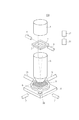
図1は、本発明の一側面としての照明光学系と投影光学系で構成されている光学系を有する露光装置100の構成を示す図である。露光装置100は、原版としてのレチクル(マスク)のパターンを投影光学系によって基板(基板上のショット領域)に投影し、レチクルのパターンを基板に転写するリソグラフィ装置である。   FIG. 1 is a view showing the arrangement of an exposure apparatus 100 having an optical system composed of an illumination optical system and a projection optical system as one aspect of the present invention. The exposure apparatus 100 is a lithography apparatus that projects a reticle (mask) pattern as an original onto a substrate (shot area on the substrate) by a projection optical system, and transfers the reticle pattern onto the substrate.

露光装置100は、図1に示すように、光源11からの光でレチクル2を照明する照明光学系1と、基板(ウエハ、ガラス基板など)9に転写すべきパターン(回路パターン)を有するレチクル2を保持して移動するレチクルステージ3を備えている。また、更に露光装置100は、アライメント検出部4を有する。アライメント検出部4は、レチクルステージ3に保持されたレチクル2の位置、及び、投影光学系5を介して基板9のアライメントマークの位置を検出する。本実施形態では、アライメント検出部4は、レチクルステージ3に保持されたレチクル2の位置を検出する機能と、基板9のアライメントマークの位置を検出する機能とを兼ね備えている。但し、レチクルステージ3に保持されたレチクル2の位置を検出するレチクルアライメント検出部と、基板9のアライメントマークの位置を検出する基板アライメント検出部とを別々に配置してもよい。   As shown in FIG. 1, an exposure apparatus 100 includes an illumination optical system 1 that illuminates a reticle 2 with light from a light source 11, and a reticle having a pattern (circuit pattern) to be transferred to a substrate (wafer, glass substrate, etc.) 9. A reticle stage 3 that moves while holding 2 is provided. Further, the exposure apparatus 100 includes an alignment detection unit 4. The alignment detection unit 4 detects the position of the reticle 2 held on the reticle stage 3 and the position of the alignment mark on the substrate 9 via the projection optical system 5. In the present embodiment, the alignment detection unit 4 has both a function of detecting the position of the reticle 2 held on the reticle stage 3 and a function of detecting the position of the alignment mark on the substrate 9. However, the reticle alignment detection unit that detects the position of the reticle 2 held on the reticle stage 3 and the substrate alignment detection unit that detects the position of the alignment mark on the substrate 9 may be arranged separately.

また、露光装置100は、レチクル2のパターンを基板9に投影する投影光学系5と、基板9を保持して移動する(少なくともXY平面内でX軸方向及びY軸方向に移動する)基板ステージ6と、基板ステージ6の位置を計測するレーザ干渉計7とを有する。露光装置100は、基板9を吸着(保持)するチャック8と、チャック8の下部に配置されて基板9をZ軸方向(垂直方向)に移動させる(即ち、露光時のピントを調整するための)Z軸移動機構(不図示)とを有する。更に、露光装置100は、基板ステージ6に保持された基板9のZ軸方向の位置(ピント位置)を計測するオートフォーカス部10と、CPUやメモリを含んで露光装置100の全体(基板9を露光する動作)を制御する制御部21も有している。そして、基板ステージ6上に露光光量を検出するための光検出センサ50、装置外部から、投影光学系の中心位置と遮光板駆動部の回転中心位置ずれ情報を含む、装置制御に必要なパラメータを入力可能な入力インターフェース51を有する。   The exposure apparatus 100 also has a projection optical system 5 that projects the pattern of the reticle 2 onto the substrate 9 and a substrate stage that holds and moves the substrate 9 (moves at least in the X-axis direction and the Y-axis direction in the XY plane). 6 and a laser interferometer 7 for measuring the position of the substrate stage 6. The exposure apparatus 100 is disposed under the chuck 8 for attracting (holding) the substrate 9 and moves the substrate 9 in the Z-axis direction (vertical direction) (that is, for adjusting the focus during exposure). ) Z-axis moving mechanism (not shown). Further, the exposure apparatus 100 includes an autofocus unit 10 that measures the position (focus position) in the Z-axis direction of the substrate 9 held on the substrate stage 6, and the entire exposure apparatus 100 (the substrate 9 includes the CPU 9 and the memory). A control unit 21 for controlling the exposure operation) is also provided. Then, a light detection sensor 50 for detecting the amount of exposure light on the substrate stage 6, parameters necessary for apparatus control, including information on the center position of the projection optical system and the rotation center position deviation of the light shielding plate driving unit, from outside the apparatus. An input interface 51 capable of inputting is provided.

図2は、照明光学系1の構成を詳細に示す図である。図2に示すように、照明光学系1は、本実施形態では、光源11を含む。但し、照明光学系1は、必ずしも光源11を含む必要はなく、照明光学系1と光源11とをそれぞれ別に構成してもよい。   FIG. 2 is a diagram showing the configuration of the illumination optical system 1 in detail. As shown in FIG. 2, the illumination optical system 1 includes a light source 11 in the present embodiment. However, the illumination optical system 1 does not necessarily include the light source 11, and the illumination optical system 1 and the light source 11 may be configured separately.

光源11は、本実施形態では、超高圧水銀ランプを使用するが、エキシマレーザー(KrFエキシマレーザーやArFエキシマレーザーなど)を使用してもよい。集光ミラー12は、一般的には、楕円ミラーを使用する。但し、集光ミラー12は、楕円ミラーに限定するものではなく、集光点の集光度を高めるように最適化されたファセットミラーを使用してもよい。シャッタ13は、制御部21の制御下において、開閉時間を調整することでレジスト(感光剤)が塗布された基板9への露光量を調整する。   The light source 11 uses an ultra-high pressure mercury lamp in this embodiment, but an excimer laser (KrF excimer laser, ArF excimer laser, etc.) may be used. The condensing mirror 12 generally uses an elliptical mirror. However, the condensing mirror 12 is not limited to an elliptical mirror, and a facet mirror optimized to increase the condensing degree of the condensing point may be used. Under the control of the control unit 21, the shutter 13 adjusts the exposure time of the substrate 9 coated with a resist (photosensitive agent) by adjusting the opening / closing time.

変倍リレー光学系14は、ズーム機構を有し、ハエの目レンズ15における光束径を変更する。露光装置100においては、基板9に転写するパターンに応じて投影光学系5の結像性能を最適化するために、(照明光学系1の(開口数)NA)/(投影光学系5のNA)で表されるコヒーレンスファクター(σ値)を変更する必要がある。本実施形態では、照明光学系1のNAを決めているハエの目レンズ15における光束径を変更することで、σ値を変更することができる。   The variable magnification relay optical system 14 has a zoom mechanism and changes the beam diameter of the fly-eye lens 15. In the exposure apparatus 100, in order to optimize the imaging performance of the projection optical system 5 according to the pattern transferred to the substrate 9, ((numerical aperture) NA of the illumination optical system 1) / (NA of the projection optical system 5). It is necessary to change the coherence factor (σ value) represented by In this embodiment, the σ value can be changed by changing the beam diameter of the fly-eye lens 15 that determines the NA of the illumination optical system 1.

ハエの目レンズ15は、入射面に入射した光束を波面分割し、射出面に2次光源を生成する。ハエの目レンズ15は、シリンドリカルレンズアレイに置換することが可能である。コンデンサー光学系16は、ハエの目レンズ15で波面分割された光を被照明面において重畳的に重ね合わせ、被照明面上に均一な照度分布を形成する。   The fly-eye lens 15 divides the light beam incident on the incident surface into wavefronts and generates a secondary light source on the exit surface. The fly-eye lens 15 can be replaced with a cylindrical lens array. The condenser optical system 16 superimposes the light wave-divided by the fly-eye lens 15 on the illuminated surface to form a uniform illuminance distribution on the illuminated surface.

マスキングブレード17は、コンデンサー光学系16の被照明面に配置される。マスキングブレード17は、開口を可変とする絞りで構成され、制御部21の制御下において、露光装置100がステップアンドリピート方式で繰り返して転写する1つのショット領域の形状(ショット形状)を決定する。換言すれば、マスキングブレード17は、基板上のショット領域の外縁を規定する直線状の辺より外側の領域に入射する光を遮光する。   The masking blade 17 is disposed on the illuminated surface of the condenser optical system 16. The masking blade 17 is configured by a diaphragm having a variable aperture, and determines the shape (shot shape) of one shot area to be transferred repeatedly by the exposure apparatus 100 in a step-and-repeat manner under the control of the control unit 21. In other words, the masking blade 17 blocks light incident on a region outside the linear side that defines the outer edge of the shot region on the substrate.

リレー光学系18は、マスキングブレード17の位置に形成された照度分布を遮光板19に投影する。また、リレー光学系20は、遮光板19の位置に形成された照度分布をレチクル2に投影する。   The relay optical system 18 projects the illuminance distribution formed at the position of the masking blade 17 onto the light shielding plate 19. Further, the relay optical system 20 projects the illuminance distribution formed at the position of the light shielding plate 19 onto the reticle 2.

遮光板19は、露光装置100がステップアンドリピート方式で繰り返して基板9を露光する際に、基板9の露光位置に応じてパターンが転写される領域の形状を変化させることが可能である。遮光板19は、照明光学系1における投影光学系5の物体面と共役な面或いはその近傍に配置され、基板9の外周より内側の円形境界線に重なる円弧(円弧状部分)を縁に含み、基板9の上のパターンが転写される領域を規定する。遮光板19は、照明光学系1及び投影光学系5で構成される光学系の光路上で、投影光学系5の物体面と共役な位置或いはその近傍に配置されていれば所望の遮光部としての機能を果たせる。また投影光学系5の物体面と共役な位置は、レチクル2が配置されることで決まるそのパターン面と共役な位置と言い変えることも可能である。   When the exposure apparatus 100 repeatedly exposes the substrate 9 by the step-and-repeat method, the light shielding plate 19 can change the shape of the region where the pattern is transferred according to the exposure position of the substrate 9. The light shielding plate 19 is arranged on the surface conjugate with the object surface of the projection optical system 5 in the illumination optical system 1 or in the vicinity thereof, and includes an arc (arc-shaped portion) overlapping the circular boundary inside the outer periphery of the substrate 9 at the edge. The area on the substrate 9 to which the pattern is transferred is defined. The light-shielding plate 19 is a desired light-shielding part as long as it is arranged at or near a position conjugate with the object plane of the projection optical system 5 on the optical path of the optical system composed of the illumination optical system 1 and the projection optical system 5. Can fulfill the functions of Further, the position conjugate with the object plane of the projection optical system 5 can be rephrased as the position conjugate with the pattern plane determined by the arrangement of the reticle 2.

遮光板19は、駆動部22を介して、基板9の上の外周ショット領域内において駆動される。例えば、駆動部22は、制御部21の制御下において、照明光学系1の光軸に平行な軸回りに遮光板19を回転駆動させたり、照明光学系1の光軸に垂直な平面内で遮光板19を直線駆動させたりする。なお、本実施形態では、配置上の都合から、マスキングブレード17と遮光板19とを、リレー光学系18を介して、照明光学系1における互いに異なる光学的に共役な位置に配置している。しかし、配置上の問題がなければ、マスキングブレード17を遮光板19に隣接して配置しても良い。マスキングブレード17を遮光板19に隣接して配置する際に、それらが同じ位置に入らない場合には、遮光板19を基板9と光学的に共役な位置に配置し、マスキングブレード17をデフォーカスさせた位置に配置するのが望ましい。また、配置上のデフォーカス量が許容できない場合には、マスキングブレード17でショット領域における第1方向に沿った外縁を規定する直線状の辺より外側の領域に対して光が入射しないように光を遮断する。そして、ショット領域における第1方向と直交する第2方向に沿った外縁を規定する直線状の辺より外側の領域に対して光が入射しないように、レチクル2上にCrパターンで光を遮断する遮光部を設ける。さらには、ショット領域の形状はレチクル2上のCrパターンで決定し、マスキングブレード17はレチクル2上のCrパターンの剥がれなどの欠陥による転写を防止するために、ショット領域の形状より大きな領域で遮光しても良い。マスキングブレード17と遮光板19の照射系内における配置位置の順番は不問で、どちらが光源11側にあっても構わない。   The light shielding plate 19 is driven in the outer peripheral shot region on the substrate 9 via the driving unit 22. For example, the drive unit 22 rotates the light shielding plate 19 around an axis parallel to the optical axis of the illumination optical system 1 under the control of the control unit 21 or within a plane perpendicular to the optical axis of the illumination optical system 1. The light shielding plate 19 is driven linearly. In the present embodiment, for convenience of arrangement, the masking blade 17 and the light shielding plate 19 are arranged at different optically conjugate positions in the illumination optical system 1 via the relay optical system 18. However, if there is no problem in arrangement, the masking blade 17 may be arranged adjacent to the light shielding plate 19. When the masking blade 17 is disposed adjacent to the light shielding plate 19 and does not enter the same position, the light shielding plate 19 is disposed at a position optically conjugate with the substrate 9 and the masking blade 17 is defocused. It is desirable to arrange at the position. If the defocus amount in the arrangement is not acceptable, the masking blade 17 does not allow light to enter a region outside the linear side that defines the outer edge along the first direction in the shot region. Shut off. Then, the light is blocked by the Cr pattern on the reticle 2 so that the light does not enter the region outside the linear side defining the outer edge along the second direction orthogonal to the first direction in the shot region. A light shielding part is provided. Further, the shape of the shot area is determined by the Cr pattern on the reticle 2, and the masking blade 17 shields light in an area larger than the shape of the shot area in order to prevent transfer due to defects such as peeling of the Cr pattern on the reticle 2. You may do it. The order of the arrangement positions of the masking blade 17 and the light shielding plate 19 in the irradiation system is not limited, and either may be on the light source 11 side.

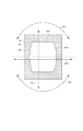
遮光板19について詳細に説明する。図3(a)は、基板9の上の転写領域を説明するための図であって、紙面上方向から見た基板9を示している。基板9には、通常、シリコン製の基板が使用されるが、ガラス製の基板、サファイヤ製の基板、化合物からなる基板も使用される。露光装置100が1回の露光でパターンを転写できる領域は、投影光学系5の結像領域で決まるが、一般的には、基板9の大きさより小さい。従って、露光装置100では、ステップアンドリピート方式と呼ばれる基板9をステップさせながらパターンの転写(基板9の露光)を繰り返す露光方式が用いられる。図3(a)に斜線で示す領域は1回の露光でパターンが転写されるショット領域を示しており、基板9をステップさせながら複数のショット領域を繰り返し露光することで、基板9の全体に同一のパターン「C」を転写することができる。   The light shielding plate 19 will be described in detail. FIG. 3A is a diagram for explaining a transfer region on the substrate 9 and shows the substrate 9 viewed from above in the drawing. As the substrate 9, a silicon substrate is usually used, but a glass substrate, a sapphire substrate, and a substrate made of a compound are also used. The area where the exposure apparatus 100 can transfer the pattern in one exposure is determined by the imaging area of the projection optical system 5, but is generally smaller than the size of the substrate 9. Therefore, the exposure apparatus 100 uses an exposure method called step-and-repeat method that repeats pattern transfer (exposure of the substrate 9) while stepping the substrate 9. 3A shows a shot area where a pattern is transferred by a single exposure. By repeatedly exposing a plurality of shot areas while stepping the substrate 9, the entire area of the substrate 9 can be obtained. The same pattern “C” can be transferred.

上述したように、はんだボールを形成する工程において、基板9の上の導電性膜とメッキ装置の電極とを接触(導通)させるためには、レジストが剥離された領域が基板9の上に存在しなければならない。かかる領域は、図3(a)に示すように、基板9の周辺部、具体的は、基板9の外周から所定の幅(本実施形態では、d)だけ内側の外周領域92に相当する。基板9の外周領域92は、基板9に塗布されたレジストがネガレジストである場合には、露光中に遮光されている必要がある。換言すれば、基板9の外周ショット領域91にパターンを転写する際には、外周ショット領域91を図3(b)に示すような転写領域、すなわちショットの外縁の一部を円弧状に規定して露光する必要がある。   As described above, in the step of forming the solder balls, in order to make the conductive film on the substrate 9 and the electrode of the plating apparatus contact (conduct), there is a region where the resist is peeled off on the substrate 9. Must. As shown in FIG. 3A, such a region corresponds to a peripheral portion of the substrate 9, specifically, an outer peripheral region 92 that is a predetermined width (in this embodiment, d) from the outer periphery of the substrate 9. When the resist applied to the substrate 9 is a negative resist, the outer peripheral region 92 of the substrate 9 needs to be shielded from light during exposure. In other words, when the pattern is transferred to the outer peripheral shot area 91 of the substrate 9, the outer peripheral shot area 91 is defined as a transfer area as shown in FIG. Need to be exposed.

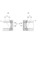
図4は、外周ショット領域91を図3(b)に示すような転写領域に規定するための遮光板19の構成の一例を示す図であって、照明光学系1の光軸方向から見た遮光板19を示している。遮光板19は、露光光を遮光する遮光部分191と、露光光を通過させる開口部分192とで構成される。遮光部分191は、基板9の外周(外縁)の円弧形状と略同一な円弧形状の円弧縁部191aと、基板9の外周領域92の遮光には直接寄与しない直線形状の直線縁部191bとを含む枠体である。理想的には、遮光板19の円弧状部分である円弧縁部191aは、上述のように基板9の外周(外縁)の円弧形状の部分の円形状の半径(曲率半径)よりもdだけ小さい円形状と略同一な円弧形状であることが望ましい。   FIG. 4 is a diagram showing an example of the configuration of the light shielding plate 19 for defining the outer peripheral shot area 91 as a transfer area as shown in FIG. 3B, as viewed from the optical axis direction of the illumination optical system 1. A light shielding plate 19 is shown. The light shielding plate 19 includes a light shielding portion 191 that shields the exposure light, and an opening portion 192 that allows the exposure light to pass through. The light shielding portion 191 includes an arc-shaped arc edge portion 191 a that is substantially the same as the arc shape of the outer periphery (outer edge) of the substrate 9, and a linear straight edge portion 191 b that does not directly contribute to the light shielding of the outer peripheral region 92 of the substrate 9. It is a frame that contains it. Ideally, the arc edge portion 191a that is the arc-shaped portion of the light shielding plate 19 is smaller by d than the circular radius (curvature radius) of the arc-shaped portion of the outer periphery (outer edge) of the substrate 9 as described above. It is desirable that the arc shape is substantially the same as the circular shape.

また、開口部分192は、露光するショット領域を照明するために必要な光束よりも太い光束が通過可能である十分な大きさを有している。基板9の中心付近のショットを露光する(パターンの像を投影)場合には、遮光板19は退避させ、ショットの露光に寄与する光束よりも太い光束が開口部分192を通る位置に移動させる。その際、光束は、遮光板19ではなく他の遮光部材であるマスキングブレード17でその断面が矩形に規定される。但し、遮光板19は、図4に示す構成に限定されるものではなく、円形形状の縁部を含む遮光部分で構成されてもよいし、一部だけが円弧形状の縁部を含む遮光部分で構成されてもよい。   The opening 192 has a sufficient size that allows a light beam thicker than the light beam necessary for illuminating the shot area to be exposed to pass. When exposing a shot near the center of the substrate 9 (projecting a pattern image), the light shielding plate 19 is retracted, and the light beam thicker than the light beam contributing to the exposure of the shot is moved to a position passing through the opening 192. At that time, the cross section of the light beam is defined by a masking blade 17 which is not a light shielding plate 19 but another light shielding member. However, the light shielding plate 19 is not limited to the configuration shown in FIG. 4, and may be composed of a light shielding portion including a circular edge, or only a part of the light shielding portion includes an arc-shaped edge. It may be constituted by.

これは、駆動部22が遮光板19を照明光学系1の光軸を中心とした回転方向(矢印AR1)に回転駆動させたり、円弧縁部191aの頂点を結ぶ直線に平行な方向(矢印AR2)に直線駆動させたりすることが可能だからである。また、駆動部22は遮光板19を、回転軸を中心として回転方向(矢印AR1)に回転駆動する回転駆動部と円弧縁部191aの頂点を結ぶ直線に平行な方向(矢印AR2)にシフト駆動(並進駆動)するシフト駆動部の2つの機構を持つ。さらに円弧縁部191aの頂点を結ぶ直線に垂直な方向(矢印AR3)にシフト駆動するもう一つ他のシフト駆動部の機構を持ってもよい。   This is because the drive unit 22 drives the light shielding plate 19 to rotate in the rotation direction (arrow AR1) about the optical axis of the illumination optical system 1, or the direction parallel to the straight line connecting the vertices of the arc edge 191a (arrow AR2). This is because it can be driven linearly. The driving unit 22 shifts the light shielding plate 19 in a direction (arrow AR2) parallel to a straight line connecting the rotation driving unit that rotates in the rotation direction (arrow AR1) about the rotation axis and the vertex of the arc edge 191a. It has two mechanisms of a shift drive part (translation drive). Furthermore, another shift drive mechanism that performs shift drive in a direction (arrow AR3) perpendicular to a straight line connecting the vertices of the arc edge 191a may be provided.

図5は、制御部21の制御下における駆動部22による遮光板19の位置決めを説明するための図であって、基板9の外周ショット領域91と遮光板19との位置関係を示している。図5に示すように、外周ショット領域91を露光する際には、基板9の外周(外縁)から幅dだけ内側の外周付近(外縁付近)にある外周領域92に入射する露光光を遮光する位置に遮光板19を位置決めする。詳細には、照明光学系1の光軸を中心としてθだけ遮光板19を回転駆動し、且つ、外周ショット領域91の中心(x1,y1)から基板9の中心方向にLだけシフト(直線駆動)した位置に遮光板19の中心(x,y)が位置するように、遮光板19を位置決めする。ここでの外周ショット領域91の中心とは、外周ショット領域91を中心部と同じように一部を円弧に遮光しない状態でのショット領域としての中心のことである。基本的には照明光学系1と投影光学系5からなる光学系の光軸は、ショット領域91の露光時には、このショット領域91の中心を通り、レチクルのパターン部分の中心を通るように配置される。   FIG. 5 is a diagram for explaining the positioning of the light shielding plate 19 by the drive unit 22 under the control of the control unit 21 and shows the positional relationship between the outer peripheral shot region 91 of the substrate 9 and the light shielding plate 19. As shown in FIG. 5, when exposing the outer peripheral shot region 91, exposure light incident on the outer peripheral region 92 located near the outer periphery (near the outer edge) by the width d from the outer periphery (outer edge) of the substrate 9 is shielded. The light shielding plate 19 is positioned at the position. More specifically, the light shielding plate 19 is rotationally driven by θ around the optical axis of the illumination optical system 1 and is shifted by L from the center (x1, y1) of the outer peripheral shot region 91 toward the center of the substrate 9 (linear driving). ), The light shielding plate 19 is positioned so that the center (x, y) of the light shielding plate 19 is located. Here, the center of the outer peripheral shot area 91 is the center of the outer peripheral shot area 91 as a shot area in a state where a part of the outer peripheral shot area 91 is not shielded by an arc as in the central portion. Basically, the optical axis of the optical system including the illumination optical system 1 and the projection optical system 5 is arranged so as to pass through the center of the shot area 91 and the center of the pattern portion of the reticle when the shot area 91 is exposed. The

なお、Lは、遮光板19の直線駆動量であって、図5に示す数値を用いて、以下の式1で表される。   Note that L is a linear drive amount of the light shielding plate 19, and is expressed by the following formula 1 using the numerical values shown in FIG.

Figure 0005868094
Figure 0005868094

d:外周領域92の幅
θ:遮光板19の回転駆動量(即ち、基板9の中心と外周ショット領域91の中心とを結ぶ直線と基板9の水平線とのなす角度)
L:遮光板19の直線駆動量
L1:遮光板19の中心から遮光板19の円弧縁部191aまでの距離
L2:基板9の中心から外周ショット領域91の中心までの距離
L3:基板9の中心から基板9の外周までの距離(即ち、基板9の半径)
L4:基板9の中心から遮光板19の中心までの距離
d: Width of outer peripheral region 92 θ: Amount of rotational drive of light shielding plate 19 (ie, angle formed by a straight line connecting the center of substrate 9 and the center of outer peripheral shot region 91 and the horizontal line of substrate 9)
L: Linear drive amount of the light shielding plate 19 L1: Distance from the center of the light shielding plate 19 to the arc edge 191a of the light shielding plate 19 L2: Distance from the center of the substrate 9 to the center of the outer peripheral shot region 91 L3: Center of the substrate 9 Distance from the outer periphery of the substrate 9 (ie, the radius of the substrate 9)
L4: Distance from the center of the substrate 9 to the center of the light shielding plate 19

図6を参照して、露光装置100による露光処理について説明する。かかる露光処理は、制御部21が露光装置100の各部を統括的に制御することで行われる。ここでは、1枚の基板9に対する露光処理を例に説明する。   With reference to FIG. 6, the exposure process by the exposure apparatus 100 will be described. Such exposure processing is performed by the control unit 21 controlling the respective units of the exposure apparatus 100 in an integrated manner. Here, an exposure process for one substrate 9 will be described as an example.

S602では、基板9の露光処理に関する露光処理情報(即ち、基板9を露光する際に必要となる情報)を取得する。露光処理情報は、露光条件などの他に、遮光板19の位置決め(制御)に必要な情報を含む。露光処理情報は、例えば、露光処理の対象となる基板9にレイヤ(下地)が形成されているかどうか(即ち、第1シーケンスであるか第2シーケンスであるか)を表すシーケンス情報、基板9の上の複数のショット領域の配列を表すレイアウト情報などを含む。また、露光処理情報は、基板9を基板ステージ6に配置する際に生じる基板9の中心と基板ステージ6の中心とのずれ量を表す基板配置オフセットや外周ショット領域91を露光する際の遮光板19の制御モードを表す遮光板制御モード情報などを含んでもよい。   In S602, exposure processing information related to the exposure processing of the substrate 9 (that is, information necessary for exposing the substrate 9) is acquired. The exposure processing information includes information necessary for positioning (control) of the light shielding plate 19 in addition to the exposure conditions. The exposure processing information includes, for example, sequence information indicating whether a layer (base) is formed on the substrate 9 to be subjected to exposure processing (that is, whether the first sequence or the second sequence), It includes layout information representing the arrangement of the plurality of shot areas above. Further, the exposure processing information includes a substrate arrangement offset indicating the amount of deviation between the center of the substrate 9 and the center of the substrate stage 6 that occurs when the substrate 9 is arranged on the substrate stage 6, and a light shielding plate when exposing the outer peripheral shot region 91. Light shielding plate control mode information representing 19 control modes may be included.

S604では、基板搬送ロボットを介して露光処理の対象となる基板9を露光装置100に搬入し、かかる基板9を基板ステージ6に配置する。この際、露光処理情報に含まれる基板配置オフセットを考慮して、基板9の中心と基板ステージ6の中心とが一致するように、基板ステージ6に基板9を保持させる。   In step S <b> 604, the substrate 9 to be subjected to exposure processing is carried into the exposure apparatus 100 via the substrate transport robot, and the substrate 9 is placed on the substrate stage 6. At this time, the substrate 9 is held on the substrate stage 6 so that the center of the substrate 9 coincides with the center of the substrate stage 6 in consideration of the substrate arrangement offset included in the exposure processing information.

S606では、S602で取得した露光処理条件に含まれるシーケンス情報に基づいて、露光処理の対象となる基板9にレイヤが形成されているかどうかを判定する。基板9にレイヤが形成されている場合には、S612に移行する。また、基板9にレイヤが形成されていない場合には、S608に移行する。   In S606, based on the sequence information included in the exposure processing condition acquired in S602, it is determined whether or not a layer is formed on the substrate 9 to be subjected to exposure processing. If a layer is formed on the substrate 9, the process proceeds to S612. If the layer is not formed on the substrate 9, the process proceeds to S608.

S608では、基板9に形成されたレイヤのアライメントマークをアライメント検出部4で検出(粗検)する(即ち、プリアライメントを行う)。S610では、S608における検出結果に基づいて、基板9に形成されたレイヤのアライメントマークをアライメント検出部4で精密に検出(精検)する。後述するように、S608及びS610における検出結果から、基板ステージ6の中心位置に相当する基板9の中心位置(基板中心位置)と基板9に形成されたレイヤにおける複数のショット領域の配列の中心位置(レイヤ中心位置)とのずれ量を求めることができる。   In S608, the alignment mark of the layer formed on the substrate 9 is detected (roughly detected) by the alignment detection unit 4 (that is, pre-alignment is performed). In S610, based on the detection result in S608, the alignment mark of the layer formed on the substrate 9 is precisely detected (examined) by the alignment detection unit 4. As will be described later, based on the detection results in S608 and S610, the center position of the substrate 9 (substrate center position) corresponding to the center position of the substrate stage 6 and the center position of the arrangement of a plurality of shot regions in the layer formed on the substrate 9 The amount of deviation from (layer center position) can be obtained.

S612では、遮光板19を駆動部22で駆動して遮光板19を位置決めする。具体的には、露光処理の対象となる基板9にレイヤが形成されていない場合には、S602で取得した露光処理条件に含まれるレイアウト情報に基づいて、図5を用いて説明したように、遮光板19を位置決めする。また、露光処理の対象となる基板9にレイヤが形成されている場合には、S602で取得した露光処理条件に含まれるレイアウト情報とS608やS610での検出結果から求まる基板中心位置とレイヤ中心位置とのずれ量とに基づいて、遮光板19を位置決めする。但し、上述したように、遮光板19は、基板9の外周ショット領域91を露光する際に、外周領域92に入射する露光光を遮光するために用いられる。従って、対象ショット領域(これからパターンを転写するショット領域)が外周ショット領域91でない場合には、照明光学系1の光路から遮光板19を退避させればよく、遮光板19を厳密に位置決めする必要はない。   In S <b> 612, the light shielding plate 19 is driven by the drive unit 22 to position the light shielding plate 19. Specifically, when a layer is not formed on the substrate 9 to be exposed, as described with reference to FIG. 5 based on the layout information included in the exposure processing condition acquired in S602, The light shielding plate 19 is positioned. When a layer is formed on the substrate 9 to be exposed, the substrate center position and the layer center position obtained from the layout information included in the exposure processing conditions acquired in S602 and the detection results in S608 and S610. The light shielding plate 19 is positioned on the basis of the deviation amount. However, as described above, the light shielding plate 19 is used to shield exposure light incident on the outer peripheral region 92 when the outer peripheral shot region 91 of the substrate 9 is exposed. Therefore, when the target shot area (shot area where the pattern is to be transferred from now on) is not the peripheral shot area 91, the light shielding plate 19 may be retracted from the optical path of the illumination optical system 1, and the light shielding plate 19 needs to be positioned precisely. There is no.

外周ショット(周辺ショットともいう)領域91でない場合、つまり基板中心部のショットを露光する場合には、枠体である遮光板19の開口192を通過した光束をマスキングブレード17で遮光する。マスキングブレード17により形成された開口部分を通過した光束が基板9に到達して基板を露光することになる。遮光板19は、光束がマスキングブレード17で遮光され、矩形領域として基板9上に投影される位置になるように位置決めされればよい。また、遮光板19の位置決めは、基板9の上の対象ショット領域を露光位置に位置させるために必要となる基板ステージ6の移動と並行して実施することが可能である。   When the area 91 is not an outer peripheral shot (also referred to as peripheral shot) area 91, that is, when a shot at the center of the substrate is exposed, the light beam that has passed through the opening 192 of the light shielding plate 19 that is a frame is shielded by the masking blade 17. The light beam that has passed through the opening formed by the masking blade 17 reaches the substrate 9 to expose the substrate. The light shielding plate 19 may be positioned so that the light beam is shielded by the masking blade 17 and is projected onto the substrate 9 as a rectangular area. Further, the positioning of the light shielding plate 19 can be performed in parallel with the movement of the substrate stage 6 necessary for positioning the target shot area on the substrate 9 at the exposure position.

S614では、基板9の上の対象ショット領域を露光して、かかる対象ショット領域にレチクル2のパターンを転写する。S616では、基板ステージ6に保持された基板9の上の全てのショット領域を露光したか(即ち、全てのショット領域にパターンを転写したか)どうかを判定する。基板9の上の全てのショット領域を露光していない場合には、次のショット領域を対象ショット領域としてS612に移行する。また、基板9の上の全てのショット領域を露光した場合には、S614に移行する。S618では、基板搬送ロボットを介して全てのショット領域が露光された基板9を回収し、かかる基板9を露光装置100から搬出する。   In S614, the target shot area on the substrate 9 is exposed, and the pattern of the reticle 2 is transferred to the target shot area. In S616, it is determined whether all the shot areas on the substrate 9 held on the substrate stage 6 have been exposed (that is, whether the pattern has been transferred to all the shot areas). If all the shot areas on the substrate 9 have not been exposed, the process proceeds to S612 with the next shot area as the target shot area. If all the shot areas on the substrate 9 have been exposed, the process proceeds to S614. In step S618, the substrate 9 on which all shot areas are exposed is collected via the substrate transport robot, and the substrate 9 is unloaded from the exposure apparatus 100.

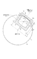
図7は、図4に示したAR3の駆動機能を持たないシステムにおいて、一つの平面(基板9面、或いはそれと平行な面)上において遮光板の回転中心である回転軸の位置が光軸の位置から(Δx、Δy)だけずれている場合について説明する。制御部21の制御下における駆動部22による遮光板19の位置決めを説明するための説明図である。光軸は、光学系によりレチクル2のパターンの像を基板9に投影する際の基準となる軸(基準軸)である。ここで、光軸とは光学系の光軸と捉えても良い。さらには、より厳密に露光装置において、光源の調整や各種位置合わせ用のマークを用いたキャリブレーションを行い、基板9上のショット領域の中心とそのショット領域に投影されるレチクル2のパターン領域の中心を通る軸と捉えても良い。   FIG. 7 shows a system that does not have the AR3 driving function shown in FIG. 4, and the position of the rotation axis that is the rotation center of the light shielding plate on one plane (the surface of the substrate 9 or a surface parallel thereto) is the optical axis. A case where the position is shifted by (Δx, Δy) will be described. FIG. 6 is an explanatory diagram for explaining positioning of the light shielding plate 19 by the driving unit 22 under the control of the control unit 21. The optical axis is an axis (reference axis) that serves as a reference when the pattern image of the reticle 2 is projected onto the substrate 9 by the optical system. Here, the optical axis may be regarded as the optical axis of the optical system. Furthermore, in the exposure apparatus, calibration using light source adjustment and various alignment marks is performed more strictly, and the center of the shot area on the substrate 9 and the pattern area of the reticle 2 projected onto the shot area are determined. It may be considered as an axis passing through the center.

遮光板19の回転中心である回転軸が光軸から(Δx、Δy)だけずれている場合、遮光板19は191aの位置に配置され外周ショット領域91を遮光すべきである。しかし、そのずれ量のため、点線で示した遮光板の回転中心である回転軸のずれ量が(Δx,Δy)の場合には、遮光板19の位置が点線で示した191bの位置にずれて配置される。そこで、正しく191aの位置に遮光板19を配置するために、図5で説明したθ、Lを計算する手順において、仮想の外周ショット領域91‘を計算する。
x2=x1−Δx
y2=y1−Δy
When the rotation axis that is the rotation center of the light shielding plate 19 is deviated from the optical axis by (Δx, Δy), the light shielding plate 19 should be disposed at a position 191a to shield the outer peripheral shot area 91. However, due to the amount of deviation, when the amount of deviation of the rotation axis that is the rotation center of the light shielding plate indicated by the dotted line is (Δx, Δy), the position of the light shielding plate 19 is shifted to the position of 191b indicated by the dotted line. Arranged. Therefore, in order to correctly arrange the light shielding plate 19 at the position of 191a, the virtual outer peripheral shot region 91 ′ is calculated in the procedure of calculating θ and L described in FIG.
x2 = x1−Δx
y2 = y1−Δy

この仮想外周ショット中心(x2,y2)に対して、図5で説明した方法でθ‘、Lを算出する。
θ‘:遮光板19の回転駆動量(即ち、基板9の中心と外周ショット領域91‘の中心とを結ぶ直線と基板9の水平線とのなす角度)
L:仮想の外周ショット領域91‘における遮光板19の直線駆動量
With respect to the virtual outer periphery shot center (x2, y2), θ ′ and L are calculated by the method described in FIG.
θ ′: A rotational driving amount of the light shielding plate 19 (that is, an angle formed by a straight line connecting the center of the substrate 9 and the center of the outer peripheral shot region 91 ′ and the horizontal line of the substrate 9).
L: A linear driving amount of the light shielding plate 19 in the virtual outer periphery shot region 91 ′

このθ‘、Lで遮光板19を駆動した場合の仮想遮光板位置は点線で示した位置となる。ここで、実際に遮光される位置は、遮光板の回転中心ずれ量が(Δx、Δy)となるので、(Δx、Δy)だけずれた191aの位置に遮光板が配置されることになる。Δx、Δyは、実施例2で説明する方法により算出された値を入力インターフェース51から入力する方法、実施例3で算出する方法のいずれであっても良い。入力インターフェース51は、装置に設けられたユーザーインターフェースであっても、ネットワーク経由で受信する方法のいずれであっても良い。   The virtual light shielding plate position when the light shielding plate 19 is driven with θ ′ and L is the position indicated by the dotted line. Here, since the rotational center shift amount of the light shielding plate is (Δx, Δy) at the position where light is actually shielded, the light shielding plate is arranged at a position of 191a shifted by (Δx, Δy). Δx and Δy may be either a method of inputting values calculated by the method described in the second embodiment from the input interface 51 or a method of calculating in the third embodiment. The input interface 51 may be either a user interface provided in the apparatus or a method of receiving via a network.

遮光板の回転中心ずれ量(Δx、Δy)は、光軸と遮光板19の回転軸との相対位置を表す情報であり、ずれの方向とずれの量である。前記相対位置を表す情報は、ステージ座標系の座標、基板座標系の座標として、所定の基準からの座標情報として取得しても良い。この相対位置を表す情報は、実施例2の算出する手段、実施例3の算出手段、入力インターフェースにより入力され露光装置100の不図示のメモリ(記憶手段)に記憶するといった取得部により取得されるものである。   The rotation center deviation amount (Δx, Δy) of the light shielding plate is information representing the relative position between the optical axis and the rotation axis of the light shielding plate 19, and is the direction and amount of deviation. The information representing the relative position may be acquired as coordinate information from a predetermined reference as coordinates in the stage coordinate system and coordinates in the substrate coordinate system. The information indicating the relative position is acquired by a calculation unit according to the second embodiment, a calculation unit according to the third embodiment, and an acquisition unit that is input through an input interface and stores the information in a memory (storage unit) (not illustrated) of the exposure apparatus 100. Is.

図4に示したAR3の駆動機能を持つシステムにおいては、Δx、Δyの遮光板の回転中心ずれ量を、回転角θの補正を行わず、AR2とAR3の駆動量により補正することも可能である。   In the system having the AR3 drive function shown in FIG. 4, it is also possible to correct the rotation center deviation amount of the light shielding plate of Δx and Δy by the drive amounts of AR2 and AR3 without correcting the rotation angle θ. is there.

[実施例2]
遮光板19は、図8のように、開口を有し、開口の縁に互いに反対側の位置に配置された第1円弧と第2円弧とを含み、第1円弧及び第2円弧は、開口の内側から外側に向かう方向に凸状をなしている。図8の例では、駆動部22の例として直線駆動部95が回転駆動部96上に搭載されることで、遮光板19を光軸として動径方向と回転方向に駆動することが可能である。なお、遮光板19を光軸として動径方向と回転方向に駆動できるようになっていれば他の形態であっても構わない。図8にAで示した点線で囲まれた領域は、遮光板19上でのショット領域を遮光した様子示しており、遮光板19で遮光された形状がウエハ上に転写される。
[Example 2]
As shown in FIG. 8, the light shielding plate 19 has an opening, and includes a first arc and a second arc arranged at opposite positions on the edge of the opening, and the first arc and the second arc are openings. It has a convex shape in the direction from the inside to the outside. In the example of FIG. 8, the linear drive unit 95 is mounted on the rotation drive unit 96 as an example of the drive unit 22, and can be driven in the radial direction and the rotation direction with the light shielding plate 19 as the optical axis. . It should be noted that other forms may be used as long as the light shielding plate 19 can be driven in the radial direction and the rotational direction with the optical axis as the optical axis. A region surrounded by a dotted line indicated by A in FIG. 8 shows a state where the shot region on the light shielding plate 19 is shielded, and the shape shielded by the light shielding plate 19 is transferred onto the wafer.

遮光板19はさらに開口部あるいは遮光部を有する。開口部あるいは遮光部は、駆動部96の回転駆動量を識別する回転駆動量識別部として機能する。なお、開口部あるいは遮光部を使用した回転駆動量の算出方法に関しては本実施例の中で明らかにされる。図9に遮光板19の開口部、遮光部の一例を示す。図9(a)の例では、遮光板19には開口部の一例として、直線部を縁に含むスリット形状の開口部61が構成されている。図9(b)のように、直線部を縁に含むスリット形状の開口部62a、62bが上下に分割されていてもよい。   The light shielding plate 19 further has an opening or a light shielding portion. The opening or the light shielding unit functions as a rotational drive amount identification unit that identifies the rotational drive amount of the drive unit 96. The calculation method of the rotational drive amount using the opening or the light shielding part will be clarified in this embodiment. FIG. 9 shows an example of an opening and a light shielding part of the light shielding plate 19. In the example of FIG. 9A, the light shielding plate 19 includes a slit-shaped opening 61 that includes a straight portion as an edge as an example of the opening. As shown in FIG. 9B, the slit-shaped openings 62a and 62b including the straight line portion at the edge may be divided vertically.

さらに図9(c)の例のように直線部を含むスリット形状ではなく、例えば丸穴形状の開口部63a、63bであってもよい。さらに言えば、開口部は開口部の形状の重心回りに点対称であれば他の形状であっても構わない。図9(d)の例では、遮光板19には遮光部の一例として、直線部を縁に含むスリット形状の遮光部71が構成されている。図9(e)のように、直線部を縁に含むスリット形状の遮光部72a、72bが上下に分割されていてもよい。図9(f)は円弧の縁に対する遮光部の長手方向が異なる場合であり、遮光部73a、73bを同じく分割して設けてもよい。なお、図9において遮光板19は第1円弧と第2円弧が別の遮光板に構成されている場合の形状であるが、もちろん図4で示したように一体の遮光板に構成されていてもよい。また、一体の遮光板の場合、開口部、遮光部は円弧と同様に対向する位置に配置すればよい。   Furthermore, instead of the slit shape including the straight portion as in the example of FIG. 9C, for example, the opening portions 63a and 63b having a round hole shape may be used. Furthermore, the opening may have another shape as long as it is point-symmetric about the center of gravity of the shape of the opening. In the example of FIG. 9D, the light shielding plate 19 is configured with a slit-shaped light shielding portion 71 that includes a straight portion as an edge as an example of the light shielding portion. As shown in FIG. 9E, slit-shaped light-shielding portions 72a and 72b that include a straight portion at the edge may be divided vertically. FIG. 9F shows a case where the light shielding portions have different longitudinal directions with respect to the edge of the arc, and the light shielding portions 73a and 73b may be divided similarly. In FIG. 9, the light shielding plate 19 has a shape in which the first arc and the second arc are formed as separate light shielding plates. Of course, the light shielding plate 19 is configured as an integral light shielding plate as shown in FIG. Also good. Further, in the case of an integral light shielding plate, the opening and the light shielding portion may be arranged at positions facing each other in the same manner as the arc.

基板9の周辺部に幅dで示した非露光領域を形成するためには、以下の2つ条件を満たす必要がある。
条件1.レチクル2と遮光板19の位置合わせが行われている(位置関係が判明している)こと。
条件2.レチクル2と基板9の位置合わせが行われている(位置関係が判明している)こと。
In order to form the non-exposed region indicated by the width d in the peripheral portion of the substrate 9, the following two conditions must be satisfied.
Condition 1. The reticle 2 and the light shielding plate 19 are aligned (the positional relationship is known).
Condition 2. The alignment between the reticle 2 and the substrate 9 is performed (the positional relationship is known).

ここでは、上記の条件2は満たしているものとして上記の条件1を実現する調整方法に関して詳細を述べる。なお、レチクル2の基準点は図1のアライメント検出部4による検出結果に基づき光軸に対して位置合わせされているものとする。下記の調整フローにおける露光処理、ステージの駆動、遮光板の駆動といった一連の処理は制御部21により行われる。   Here, it is assumed that the condition 2 is satisfied, and details regarding the adjustment method for realizing the condition 1 will be described. It is assumed that the reference point of the reticle 2 is aligned with the optical axis based on the detection result by the alignment detection unit 4 in FIG. A series of processing such as exposure processing, stage driving, and light shielding plate driving in the following adjustment flow is performed by the control unit 21.

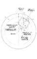
まず、図10のフローチャート1001に示すレチクル2の基準点(以下ではレチクル2の中心2cとする)と回転駆動部96の回転中心96cの位置合わせを行う。図11は上述の位置合わせに用いるレチクル2を紙面上方から見た図であり、図のようにX軸、Y軸を定義する。レチクル2には、基板上に転写可能なパターンとして、少なくとも2本の目盛り40a、40bを有しているものとする。目盛40はレチクル2の中心からのY座標が既知である。目盛40の値はレチクル2上のX座標を表している。遮光板19は図9(a)に示した形状を有するものとする。   First, alignment of the reference point of the reticle 2 (hereinafter referred to as the center 2c of the reticle 2) and the rotation center 96c of the rotation drive unit 96 shown in the flowchart 1001 of FIG. FIG. 11 is a view of the reticle 2 used for the above-described alignment as viewed from above, and the X axis and the Y axis are defined as shown in the figure. It is assumed that the reticle 2 has at least two scales 40a and 40b as patterns that can be transferred onto the substrate. The scale 40 has a known Y coordinate from the center of the reticle 2. The value of the scale 40 represents the X coordinate on the reticle 2. The light shielding plate 19 is assumed to have the shape shown in FIG.

レチクル2の中心2cと回転駆動部96の回転中心96cの位置合わせに関して、図12のフローチャートの従って詳しく説明する。なおここでは遮光板19の第1円弧を用いるものとする。ステップ2001で、レチクル、ウエハの搬入や露光量やウエハ上のレイアウト、駆動部の駆動条件などの露光条件を設定する。ステップ2002にて駆動条件に基づき遮光板19を回転駆動部96による回転駆動と直線駆動部95による直線駆動を行い、図13(a)に一例として示す第1位置に移動する。図13(a)から明らかなように第1位置ではレチクル2は遮光板19により遮光され、且つ遮光板19の第1円弧と開口部23がレチクル2上位置している。なお、図13では回転駆動部96と直線駆動部95は不図示であるが、遮光板19と回転駆動部96、直線駆動部95の関係は図8に従うものとする。合わせて、基板9を保持している基板ステージ6を駆動し、ショット位置へ駆動する。ステップ2003にて、照射系から所定の露光量を基板9上に照射する。基板9上にはレチクル2のパターンが遮光板19により規定された形状にてショットS1が転写される。ステップ2004にて、駆動部の駆動条件に基づき直線駆動軸方向は固定のまま、回転駆動部96の回転中心96c回りに180度回転駆動することで、遮光板19は第2位置(図13(b))に移動する。合わせて、基板9を保持している基板ステージ6を駆動し、次のショット位置に移動する。ステップ2005にて、同じく照射系から所定の露光量を基板9上に照射され、ショットS2が転写される。ステップ2006にて、基板9を搬出し、現像を行う。現像により基板9にはショットS1とショットS2のレジスト像が形成されている。ステップ2007では、遮光板19の第1位置のショットS1と第2位置のショットS2を基に、レチクル2の中心2cに対する回転駆動部96の回転中心96cを求める。図14(a)に示すショットS1の遮光板19の第1円弧の縁と目盛40a、40bの交点の値41a、41bを読み取り記録する。また、同時にショットS1の遮光板19の直線スリット状の開口部61の直線の縁と目盛40a、40bの交点の値42a、42bを読み取り記録する。図14(b)に示すショットS2においても同様に値(43a、43b、44a、44b)を読み取り記録する。目盛の読み取りは、例えば、汎用の光学顕微鏡を使用することができる。なお、図14においては露光された部分のレジストが現像において剥離した場合、つまりポジレジストの場合の図になっているが、ネガレジストであってもよい。図示の容易さからここではポジレジストの場合で記載している。   The alignment of the center 2c of the reticle 2 and the rotation center 96c of the rotation drive unit 96 will be described in detail with reference to the flowchart of FIG. Here, the first arc of the light shielding plate 19 is used. In step 2001, exposure conditions such as reticle and wafer carry-in, exposure amount, layout on the wafer, and drive conditions of the drive unit are set. In step 2002, the light shielding plate 19 is rotationally driven by the rotational drive unit 96 and linearly driven by the linear drive unit 95 based on the drive conditions, and moved to the first position shown as an example in FIG. As is clear from FIG. 13A, the reticle 2 is shielded by the light shielding plate 19 at the first position, and the first arc and the opening 23 of the light shielding plate 19 are located on the reticle 2. In FIG. 13, the rotation drive unit 96 and the linear drive unit 95 are not shown, but the relationship between the light shielding plate 19, the rotation drive unit 96, and the linear drive unit 95 is as shown in FIG. At the same time, the substrate stage 6 holding the substrate 9 is driven and driven to the shot position. In step 2003, a predetermined exposure dose is irradiated onto the substrate 9 from the irradiation system. On the substrate 9, the shot S1 is transferred in a shape in which the pattern of the reticle 2 is defined by the light shielding plate 19. In step 2004, the light shielding plate 19 is rotated to 180 degrees around the rotation center 96c of the rotation driving unit 96 while the linear drive axis direction is fixed based on the driving condition of the driving unit. Go to b)). At the same time, the substrate stage 6 holding the substrate 9 is driven to move to the next shot position. In step 2005, the substrate 9 is irradiated with a predetermined exposure amount from the irradiation system, and the shot S2 is transferred. In step 2006, the substrate 9 is unloaded and developed. As a result of development, resist images of shot S1 and shot S2 are formed on the substrate 9. In step 2007, based on the shot S1 at the first position and the shot S2 at the second position of the light shielding plate 19, a rotation center 96c of the rotation drive unit 96 with respect to the center 2c of the reticle 2 is obtained. The values 41a and 41b of the intersection points of the first arc edge of the light shielding plate 19 of the shot S1 shown in FIG. 14A and the scales 40a and 40b are read and recorded. At the same time, the values 42a and 42b of the intersections of the straight edges of the linear slit-shaped openings 61 of the light shielding plate 19 of the shot S1 and the scales 40a and 40b are read and recorded. Similarly, the values (43a, 43b, 44a, 44b) are read and recorded in the shot S2 shown in FIG. For example, a general-purpose optical microscope can be used to read the scale. In FIG. 14, the exposed portion of the resist is peeled off during development, that is, a positive resist, but a negative resist may be used. For ease of illustration, a positive resist is used here.

上述のように目盛40はレチクル2の中心基準の座標値を表している。まず第1位置のショットS1の目盛の値41a、41bと第1円弧の半径から第1円弧が作る第1円の中心座標Oaを計算する。同じく、第2位置のショットS2の目盛の値43a、43bと第1円弧の半径から第1円弧が作る第2円の中心座標Obを計算する。第1円と第2円の中心座標Oa,Obの中点Oが、回転駆動部96の回転中心である。これをもとにレチクル2の中心と回転駆動部96の回転中心を合わせるように位置調整を行う。   As described above, the scale 40 represents the coordinate value of the center reference of the reticle 2. First, the center coordinate Oa of the first circle formed by the first arc is calculated from the scale values 41a and 41b of the shot S1 at the first position and the radius of the first arc. Similarly, the center coordinate Ob of the second circle formed by the first arc is calculated from the scale values 43a and 43b of the shot S2 at the second position and the radius of the first arc. The midpoint O of the center coordinates Oa, Ob of the first circle and the second circle is the rotation center of the rotation drive unit 96. Based on this, position adjustment is performed so that the center of the reticle 2 and the rotation center of the rotation drive unit 96 are aligned.

ところが、第1位置から第2位置に回転駆動部96で回転駆動する際には必ず回転角度に誤差がある。回転駆動部96の回転角度の誤差の要因は、駆動部の構成によりさまざまであるが、例えばモータの角度検出に使用するロータリーエンコーダ、ギアのバックラッシュなどの誤差であり、ゼロにすることは事実上できない。図13(c)は遮光板19が第1位置から180+α度(αは回転誤差)回った位置を第2位置とした時の様子を示す。図13(c)の状態で露光したショットからは第1円弧が作る第2円の中心座標Ocが得られる。第1円と第2円の中心座標Oa、Ocの中点Oeが回転駆動部96の回転中心として求められる。すなわち真の回転中心96cと異なる点を算出してしまう。図13(d)に示すように特に回転中心座標のY座標の算出精度に顕著な影響を与える。そこで同時に記録したスリット形状の開口部61の直線の縁と目盛40の交点の値を使用した補正を行う。第1位置でのスリット形状の開口部61の直線の縁と目盛40の交点の座標42a、42bの2点を通る直線の傾きT1を得る。同じく第2位置でのスリット形状の開口部61の直線の縁と目盛40の交点の座標44a、44bの2点を通る直線の傾きT2を得る。第1位置から第2位置へ正確に180度だけ遮光板19が回転していれば、両者の傾きは等しくT1=T2となる。両者の傾きの差T1−T2=αを計算することで、第1位置から第2位置へ回転した時の実回転角度が180+α度であることがわかる。次に実回転角度を用いた補正方法に関して説明する。第1位置の第1円の中心座標Oaと第2位置の第2円の中心座標OcのX方向の距離をPとする。今、回転角度180度に対回転角度誤差はα度と分かっているため、それをもとに第2位置の第2円の中心座標OcのY座標Ocyを補正する。補正量δyはPsin(α/2)で定義できる。補正後の第2位置の第2円の中心座標Odと第1位置の第1円の中心座標Oaにより回転駆動部96に回転角度誤差が存在しても回転駆動部96の回転中心96cを求める算出精度を向上させることができる。以上の結果を基に回転駆動部96の回転中心96cをレチクル2の中心2cが一致するように調整を行えばよい。なお、遮光板19の第1円弧と開口部、遮光部は同時にウエハ上へ投影することが好ましいが、その限りではない。マスキングブレード17により照明領域を制限することで、個別に基板上へ投影し、前述の回転駆動部96の回転中心とレチクル2の位置を合わせる調整を実施してもよい。また、レチクル2上の目盛40はX軸に沿って配置したが、Y軸に沿って配置されていてもかまわない。その場合は遮光板19の第1位置と第2位置は、実施例の場合からさらに90度回転した位置で行えばよい。さらに言えば、レチクル2上の目盛に応じて、適切な回転位置で行えばよい。   However, there is always an error in the rotation angle when the rotary drive unit 96 is driven to rotate from the first position to the second position. The cause of the error in the rotation angle of the rotary drive unit 96 varies depending on the configuration of the drive unit. For example, it is an error such as a rotary encoder used for detecting the motor angle and a gear backlash. I ca n’t go up. FIG. 13C shows a state in which the position where the light shielding plate 19 is rotated 180 + α degrees (α is a rotation error) from the first position is set as the second position. From the shot exposed in the state of FIG. 13C, the center coordinates Oc of the second circle formed by the first arc are obtained. The center point Oe of the center coordinates Oa, Oc of the first circle and the second circle is obtained as the rotation center of the rotation drive unit 96. That is, a point different from the true rotation center 96c is calculated. As shown in FIG. 13D, the calculation accuracy of the Y coordinate of the rotation center coordinate is particularly affected. Therefore, correction is performed using the value of the intersection of the straight edge of the slit-shaped opening 61 and the scale 40 simultaneously recorded. The slope T1 of the straight line passing through the two points of the coordinates 42a and 42b of the intersection of the straight line edge of the slit-shaped opening 61 and the scale 40 at the first position is obtained. Similarly, the slope T2 of the straight line passing through the two points of the coordinates 44a and 44b of the intersection of the scale 40 with the straight edge of the slit-shaped opening 61 at the second position is obtained. If the light shielding plate 19 is rotated exactly 180 degrees from the first position to the second position, the inclinations of both are equal to T1 = T2. By calculating the difference T1-T2 = α between the two, it can be seen that the actual rotation angle when rotating from the first position to the second position is 180 + α degrees. Next, a correction method using the actual rotation angle will be described. Let P be the distance in the X direction between the center coordinate Oa of the first circle at the first position and the center coordinate Oc of the second circle at the second position. Since the rotation angle error is known to be α degrees at a rotation angle of 180 degrees, the Y coordinate Ocy of the center coordinate Oc of the second circle at the second position is corrected based on the error. The correction amount δy can be defined by Psin (α / 2). The center of rotation 96c of the rotation drive unit 96 is obtained from the center coordinate Od of the second circle at the second position after correction and the center coordinate Oa of the first circle at the first position even if there is a rotation angle error in the rotation drive unit 96. Calculation accuracy can be improved. Based on the above results, the rotation center 96c of the rotation drive unit 96 may be adjusted so that the center 2c of the reticle 2 coincides. The first arc, the opening, and the light shielding portion of the light shielding plate 19 are preferably projected onto the wafer at the same time, but this is not restrictive. By limiting the illumination area with the masking blade 17, the projection may be individually projected onto the substrate, and the adjustment of aligning the rotation center of the rotation driving unit 96 and the position of the reticle 2 may be performed. Further, the scale 40 on the reticle 2 is arranged along the X axis, but it may be arranged along the Y axis. In this case, the first position and the second position of the light shielding plate 19 may be performed at positions rotated by 90 degrees from the case of the embodiment. Furthermore, it may be performed at an appropriate rotational position according to the scale on the reticle 2.

続いて、図10のフローチャート1002にて、遮光板19を回転駆動する回転駆動部96の駆動原点を調整する。この調整によりレチクル2のX軸と遮光板19を直線駆動する直線駆動部95の駆動軸を平行にすることができる。図13においては、簡単のため既に平行な状態で図示しているが、実際には部品の形状誤差や組立誤差があり、両者は平行ではない。前述で求めた第1円の中心座標Oaと第2円の中心座標Odを通る直線の傾きがゼロになるように回転駆動部96の駆動原点にオフセットを持たせるのがよい。なお、遮光板19の第2円弧についても同様の調整を行うものとする。   Subsequently, in the flowchart 1002 of FIG. 10, the driving origin of the rotation driving unit 96 that rotates the light shielding plate 19 is adjusted. By this adjustment, the X axis of the reticle 2 and the drive axis of the linear drive unit 95 that linearly drives the light shielding plate 19 can be made parallel. In FIG. 13, for simplicity, it is already shown in a parallel state, but in reality there are part shape errors and assembly errors, and they are not parallel. It is preferable to give an offset to the drive origin of the rotation drive unit 96 so that the slope of the straight line passing through the center coordinate Oa of the first circle and the center coordinate Od of the second circle determined above is zero. It should be noted that the same adjustment is performed for the second arc of the light shielding plate 19.

続いて、図10のフローチャート1003にて、遮光板19を直線駆動する直線駆動部95の駆動原点を調整する。この調整により直線駆動部95の駆動軸方向とレチクル2のX軸方向の位置が合う。回転駆動部96を固定して、遮光板19の第1円弧とレチクル2上の目盛40が交差する位置に直線駆動部95により遮光板19を駆動する。この状態で基板9に露光する。ウエハを搬出し、現像後、第1円弧と目盛40の交点の値を読み、指定の値になるように直線駆動部95の駆動原点にオフセットを持たせるとよい。以上の調整により、レチクル2と遮光板19の第1円弧の位置合わせは完了である。なお、遮光板19の第2円弧についても同様の調整を行えばよい。 Subsequently, in the flowchart 1003 of FIG. 10, the drive origin of the linear drive unit 95 that linearly drives the light shielding plate 19 is adjusted. By this adjustment, the position of the drive axis direction of the linear drive unit 95 and the position of the reticle 2 in the X-axis direction are matched. The rotation driving unit 96 is fixed, and the light shielding plate 19 is driven by the linear driving unit 95 at a position where the first arc of the light shielding plate 19 and the scale 40 on the reticle 2 intersect. In this state, the substrate 9 is exposed. After the wafer is unloaded and developed, the value of the intersection of the first arc and the scale 40 is read, and the drive origin of the linear drive unit 95 may be offset so as to have a specified value. With the above adjustment, the alignment of the first arc of the reticle 2 and the light shielding plate 19 is completed. The same adjustment may be performed for the second arc of the light shielding plate 19.

実施例2では、遮光板19は図(a)をもとに説明したが、図(b)、図9(c)、図9(d)、図9(e)、図9(f)の形状であっても同様に調整可能であることは明らかである。図(f)の遮光板19の場合は、遮光部73aあるいは73bの直線の縁を使って実回転角度を算出すればよい。この場合レチクル上に目盛40とは別に遮光部73aあるいは73bの直線の縁と交差する目盛をさらに構成する必要がある。また、図4で示した遮光板19の直線の縁191bがウエハ上の円弧の縁と共に投影可能であれば、同じく実回転角度の算出に使用することができる。また、実施例2では、調整に必要な最小限のショット数で説明をしたが、実際には目盛の読み取り誤差による算出精度への影響を低減させるため複数のショットの平均を用いてよく、ショット数を限定しない。また、実施例2では、レチクル2上の2つ目盛の座標と円弧の半径から円の中心座標を算出したが、レチクル上にさらに少なくとも1つの目盛を用意して3つの目盛の座標から円の中心を算出してもよい。また同じく目盛の読み取り誤差による算出精度への影響を低減させるため、複数の目盛の中から3つの目盛を選んだそれぞれの組み合わせから求めた円の中心座標の平均を用いてもよい。 In Example 2, although the light shielding plate 19 has been described based on FIG. 9 (a), FIG. 9 (b), the FIG. 9 (c), the FIG. 9 (d), the FIG. 9 (e), the FIG. 9 (f It is obvious that the shape can be adjusted in the same manner even if the shape is. For the light shielding plate 19 in FIG. 9 (f), the may calculate an actual rotational angle with an edge of the linear light-shielding portions 73 a or 73 b. In this case, it is necessary to further configure a scale on the reticle that intersects the straight edge of the light shielding portion 73 a or 73 b separately from the scale 40. If the straight edge 191b of the light shielding plate 19 shown in FIG. 4 can be projected together with the edge of the arc on the wafer, it can be used for calculating the actual rotation angle. In the second embodiment, the minimum number of shots necessary for adjustment has been described. However, in practice, an average of a plurality of shots may be used in order to reduce the influence on the calculation accuracy due to the scale reading error. The number is not limited. In the second embodiment, the center coordinates of the circle are calculated from the coordinates of the two scales on the reticle 2 and the radius of the arc. However, at least one scale is prepared on the reticle and the circle coordinates are calculated from the coordinates of the three scales. The center may be calculated. Similarly, in order to reduce the influence of the scale reading error on the calculation accuracy, an average of the center coordinates of the circles obtained from the respective combinations of the three scales selected from the plurality of scales may be used.

実施例2において、開口部あるいは遮光部は、位置調整に使用することが目的であることが理解できよう。基板9の外周から遮光幅dで規定される遮光領域を形成する際には、開口部あるいは遮光部によるウエハ上へのパターン転写は、必要ない。むしろ問題となる。すなわち遮光板19の位置調整時のみ開口部あるいは遮光部のパターン転写を行う。そのため、開口部あるいは遮光部は基板上へのパターンの転写有無を状況に応じて選択できる必要がある。具体的には、開口部を塞ぐ、遮光部は取り外すあるいはウエハ上へパターン転写が起こらない位置へ移動することにより選択ができる。なお、開口部あるいは遮光部のウエハ上へのパターンの転写有無の選択手段は、自動であっても手動であってもその方法は構わない。   In the second embodiment, it can be understood that the opening or the light shielding portion is used for position adjustment. When forming the light shielding region defined by the light shielding width d from the outer periphery of the substrate 9, it is not necessary to transfer the pattern onto the wafer by the opening or the light shielding portion. Rather it becomes a problem. That is, only when the position of the light shielding plate 19 is adjusted, the pattern of the opening or light shielding portion is transferred. Therefore, it is necessary for the opening portion or the light shielding portion to select whether or not the pattern is transferred onto the substrate according to the situation. Specifically, the selection can be made by closing the opening, removing the light shielding part, or moving to a position where pattern transfer does not occur on the wafer. The means for selecting whether or not to transfer the pattern onto the wafer at the opening or the light-shielding portion may be automatic or manual.

[実施例3]
実施例2では、図12のフローチャート1001の調整は基板9上に露光したショットから得られる情報をもとに行ったが、基板ステージ6上の光検出センサ50を使用して調整することもできる。光検出部である光検出センサ50は照射系から照射される光を受光して、ウエハ面上の露光光量を検出できるセンサである。光検出センサ50により遮光板19の縁をステージ座標基準で検出することができる。より具体的には、ステージを駆動しながら照度がゼロになる座標を検出すればよい。照度がゼロになる2つの座標と円弧の半径から同じく円の中心座標を求めることができる。同様に図(a)を例にすれば、開口部のスリットの直線部の傾きも求めることができる。遮光板19が図(c)の形状の場合は、照度検出センサを使用して、開口部63a、63bの重心位置をそれぞれ検出すればよい。開口部に直線部がなくとも2点の重心位置を結ぶ直線傾きを使うことで前述の角度補正が可能であることが容易に理解できよう。上記の光検出センサ50上への投光処理、ステージの駆動、遮光板の駆動といった一連の処理は制御部21により行われる。光検出センサ50の検出結果は制御部21内の検出演算部で処理され、回転中心のずれ量はデータベースへ登録される。以降遮光板を駆動する駆動部はデータベースに登録された回転中心のずれ量をもとに制御部21により補正駆動される。なお、照度検出センサを使用した場合はレチクルと駆動部の回転中心の関係を直接的に合わせているわけではないことに注意する必要がある。この場合は基板ステージ6上のウエハと照度検出センサの位置関係が分かっている必要があり、間接的にレチクル中心と駆動部の回転中心を合わせていることになる。また、図10のフローチャート1002、1003の調整も同様に光検出センサ50を使用して調整可能であることは理解できるであろう。
[Example 3]
In the second embodiment, the adjustment in the flowchart 1001 in FIG. 12 is performed based on the information obtained from the shot exposed on the substrate 9. However, the adjustment can be performed using the light detection sensor 50 on the substrate stage 6. . A light detection sensor 50 as a light detection unit is a sensor that can receive light emitted from an irradiation system and detect the amount of exposure light on the wafer surface. The light detection sensor 50 can detect the edge of the light shielding plate 19 on the basis of the stage coordinates. More specifically, coordinates at which the illuminance is zero may be detected while driving the stage. Similarly, the center coordinates of the circle can be obtained from the two coordinates where the illuminance becomes zero and the radius of the arc. If Similarly to the example FIG. 9 (a), it is possible to determine also the slope of the linear portion of the slit opening. When the light shielding plate 19 is in the shape of FIG. 9 (c), using the illumination detection sensor, the opening 63a, 63b of the center of gravity may be detected, respectively. It can be easily understood that the angle correction described above can be performed by using a linear inclination connecting the center of gravity of two points even if the opening does not have a linear portion. A series of processes such as the light projecting process on the light detection sensor 50, the driving of the stage, and the driving of the light shielding plate are performed by the control unit 21. The detection result of the light detection sensor 50 is processed by the detection calculation unit in the control unit 21, and the deviation amount of the rotation center is registered in the database. Thereafter, the drive unit for driving the light shielding plate is corrected and driven by the control unit 21 based on the amount of deviation of the rotation center registered in the database. It should be noted that when the illuminance detection sensor is used, the relationship between the reticle and the rotation center of the drive unit is not directly matched. In this case, the positional relationship between the wafer on the substrate stage 6 and the illuminance detection sensor needs to be known, and the reticle center and the rotation center of the drive unit are indirectly aligned. In addition, it will be understood that the adjustment of the flowcharts 1002 and 1003 in FIG. 10 can be similarly adjusted using the light detection sensor 50.

つぎに、本発明の一実施形態のデバイス(半導体デバイス、液晶表示デバイス等)の製造方法について説明する。半導体デバイスは、ウエハに集積回路を作る前工程と、前工程で作られたウエハ上の集積回路チップを製品として完成させる後工程を経ることにより製造される。前工程は、前述の露光装置を使用して感光剤が塗布されたウエハを露光する工程と、ウエハを現像する工程を含む。後工程は、アッセンブリ工程(ダイシング、ボンディング)と、パッケージング工程(封入)を含む。液晶表示デバイスは、透明電極を形成する工程を経ることにより製造される。透明電極を形成する工程は、透明導電膜が蒸着されたガラス基板に感光剤を塗布する工程と、前述の露光装置を使用して感光剤が塗布されたガラス基板を露光する工程と、ガラス基板を現像する工程を含む。本実施形態のデバイス製造方法によれば、従来よりも高品位のデバイスを製造することができる。   Next, a method for manufacturing a device (semiconductor device, liquid crystal display device, etc.) according to an embodiment of the present invention will be described. A semiconductor device is manufactured through a pre-process for producing an integrated circuit on a wafer and a post-process for completing an integrated circuit chip on the wafer produced in the pre-process as a product. The pre-process includes a step of exposing a wafer coated with a photosensitive agent using the above-described exposure apparatus, and a step of developing the wafer. The post-process includes an assembly process (dicing and bonding) and a packaging process (encapsulation). A liquid crystal display device is manufactured through a process of forming a transparent electrode. The step of forming the transparent electrode includes a step of applying a photosensitive agent to a glass substrate on which a transparent conductive film is deposited, a step of exposing the glass substrate on which the photosensitive agent is applied using the above-described exposure apparatus, and a glass substrate. The process of developing is included. According to the device manufacturing method of the present embodiment, it is possible to manufacture a higher quality device than before.

以上、本発明の好ましい実施形態について説明したが、本発明はこれらの実施形態に限定されず、その要旨の範囲内で種々の変形および変更が可能である。   As mentioned above, although preferable embodiment of this invention was described, this invention is not limited to these embodiment, A various deformation | transformation and change are possible within the range of the summary.

以上、本発明の好ましい実施形態について説明したが、本発明はこれらの実施形態に限定されないことはいうまでもなく、その要旨の範囲内で種々の変形及び変更が可能である。   As mentioned above, although preferable embodiment of this invention was described, it cannot be overemphasized that this invention is not limited to these embodiment, A various deformation | transformation and change are possible within the range of the summary.

1 照明光学系
2 レチクル
3 レチクルステージ
5 投影光学系
6 基板ステージ6
11 光源
17 マスキングブレード
19 遮光板
DESCRIPTION OF SYMBOLS 1 Illumination optical system 2 Reticle 3 Reticle stage 5 Projection optical system 6 Substrate stage 6
11 Light source 17 Masking blade 19 Shading plate

Claims (11)

原版を照明する照明光学系と、前記原版に形成されたパターンの像を基板に投影する投影光学系を有する光学系を備える露光装置であって、
前記光学系の前記投影光学系の物体面と共役な面或いはそれらの面の近傍に配置され、前記パターンの像が前記基板に投影される領域の外縁の少なくとも一部を円弧状に規定するための円弧状部分を有する遮光板と、
前記光学系の光路に沿った回転軸を回転中心として前記遮光板を回転駆動する回転駆動部と、
前記回転軸と交わる方向に前記遮光板をシフト駆動するシフト駆動部と、
前記回転駆動部により前記遮光板を回転駆動させ、前記光学系により前記パターンの像を前記基板に投影する際の基準となる基準軸と前記遮光板の回転中心である回転軸との相対位置に関する情報を取得する取得部と、
前記取得部により取得した前記相対位置に関する情報に基づいて、前記遮光板が所定の位置になるように前記回転駆動部と前記シフト駆動部を制御する制御部を有することを特徴とする露光装置。
An exposure apparatus comprising an illumination optical system for illuminating an original and an optical system having a projection optical system for projecting an image of a pattern formed on the original onto a substrate,
A surface of the optical system that is conjugated to the object plane of the projection optical system or in the vicinity of those surfaces, and for defining at least a part of the outer edge of the area where the image of the pattern is projected on the substrate in an arc shape A light shielding plate having an arc-shaped portion of
A rotary drive unit for rotating the light blocking plate as the center of rotation of the rotary axis along the optical path of the optical system,
A shift drive unit that shift-drives the light shielding plate in a direction intersecting the rotation axis;
The rotation driving unit rotates the light shielding plate, and the optical system relates to a relative position between a reference axis serving as a reference when the pattern image is projected onto the substrate and a rotation axis that is a rotation center of the light shielding plate. An acquisition unit for acquiring information;
An exposure apparatus comprising: a control unit that controls the rotation driving unit and the shift driving unit so that the light shielding plate is at a predetermined position based on information on the relative position acquired by the acquisition unit.
前記基準軸は、前記光学系の光軸、または、前記基板上のショット領域の中心と前記ショット領域に投影される前記原版のパターン領域の中心を通る軸であることを特徴とする請求項1に記載の露光装置。2. The reference axis is an optical axis of the optical system or an axis passing through a center of a shot area on the substrate and a center of a pattern area of the original projected on the shot area. The exposure apparatus described in 1. 前記シフト駆動部は、前記回転軸に直交し前記回転軸と前記円弧状部分の頂点を結ぶ直線に平行な方向に前記遮光板をシフト駆動させることを特徴とする請求項1または2に記載の露光装置。3. The shift driving unit according to claim 1, wherein the shift driving unit shifts the light shielding plate in a direction parallel to a straight line that is orthogonal to the rotation axis and connects the rotation axis and the top of the arcuate portion. Exposure device. 前記遮光板の前記円弧状部分の曲率半径は、前記基板の外縁の前記円弧状部分の曲率半径よりも小さいことを特徴とする請求項1乃至3のいずれか一項に記載の露光装置。 The radius of curvature of the arcuate portion of the light shielding plate, the exposure apparatus according to any one of claims 1 to 3, wherein the smaller than the radius of curvature of the arcuate portion of the outer edge of the substrate. 前記相対位置に関する情報は、前記基準軸に対する前記回転軸の位置ずれの方向と位置ずれの量を表す情報であることを特徴とする請求項1乃至4のいずれか一項に記載の露光装置。 Information relating to the relative position, the exposure apparatus according to any one of claims 1 to 4, characterized in that the information representing the amount of direction and position shift of the rotating shaft with respect to the reference axis. 前記制御部は、前記基準軸に対する前記回転軸の位置ずれの方向と位置ずれの量を表わす情報に基づき、仮想のショット領域の位置を求め、The control unit obtains the position of a virtual shot region based on information indicating the direction of displacement and the amount of displacement of the rotation axis with respect to the reference axis,
該仮想のショット領域の位置に基づいて、前記回転駆動部と前記シフト駆動部を制御することを特徴とする請求項5に記載の露光装置。6. The exposure apparatus according to claim 5, wherein the rotation driving unit and the shift driving unit are controlled based on the position of the virtual shot region.
前記基準軸と前記回転軸の相対位置に関する情報は、前記制御部により前記回転駆動部を制御して、前記遮光板を回転駆動し、前記遮光板をそれぞれ異なる2つの回転駆動した位置に配置することで取得することを特徴とする請求項1乃至のいずれか一項に記載の露光装置。 Information on the relative position of the reference axis and the rotation axis is obtained by controlling the rotation driving unit by the control unit to rotationally drive the light shielding plate, and dispose the light shielding plate at two different rotationally driven positions . The exposure apparatus according to any one of claims 1 to 6 , wherein the exposure apparatus is acquired by performing 前記基板を保持して移動する基板ステージを有し、前記基板ステージには光検出部が設けられており、
前記取得部は、前記遮光板をそれぞれ異なる2つの回転駆動した位置に配置した状態で光源からの光を前記光検出部により受光することで得た情報に基づいて前記相対位置に関する情報を取得することを特徴とする請求項1乃至のいずれか一項に記載の露光装置。
It has a substrate stage that moves while holding the substrate, and the substrate stage is provided with a light detection unit,
The acquisition unit acquires information on the relative position based on information obtained by receiving light from a light source by the light detection unit in a state where the light shielding plate is disposed at two different rotationally driven positions. the exposure apparatus according to any one of claims 1 to 7, characterized in that.
前記領域を規定する前記遮光板とは異なる遮光部材を有し、
前記遮光板は、中心部に開口部を有し、前記開口部の対向する位置に前記円弧状部分が形成された枠体であり、
前記基板の中心付近に対して前記パターンの像を投影する場合には、前記パターンの像の前記基板上に投影される領域に到達する光源からの光は前記枠体の前記開口部を通過しており、前記領域を前記遮光部材で規定していることを特徴とする請求項1乃至のいずれか一項に記載の露光装置。
A light shielding member different from the light shielding plate defining the region;
The light-shielding plate is a frame having an opening at a central portion and the arc-shaped portion formed at a position facing the opening,
When projecting the image of the pattern to the vicinity of the center of the substrate, light from a light source that reaches an area projected on the substrate of the pattern image passes through the opening of the frame. and which, exposure apparatus according to any one of claims 1 to 8, characterized in that defining the region in the light shielding member.
前記シフト駆動部は、前記遮光板を前記光学系の光軸に垂直な方向にシフト駆動させることを特徴とする請求項1乃至のいずれか一項に記載の露光装置。 The shift driving unit, an exposure apparatus according to the light shielding plate to any one of claims 1 to 9, wherein the shifting drive in a direction perpendicular to the optical axis of the optical system. 請求項1乃至10のうちいずれか1項に記載の露光装置を用いて基板を露光するステップと、
露光された前記基板を現像するステップと、
を有することを特徴とするデバイスの製造方法。
Exposing the substrate using the exposure apparatus according to any one of claims 1 to 10 ,
Developing the exposed substrate;
A device manufacturing method characterized by comprising:
JP2011209100A 2011-09-26 2011-09-26 Exposure apparatus and device manufacturing method Active JP5868094B2 (en)

Priority Applications (4)

Application Number Priority Date Filing Date Title
JP2011209100A JP5868094B2 (en) 2011-09-26 2011-09-26 Exposure apparatus and device manufacturing method
US13/610,308 US8625073B2 (en) 2011-09-26 2012-09-11 Exposure apparatus and device manufacturing method
TW101133761A TWI470377B (en) 2011-09-26 2012-09-14 Exposure apparatus and device manufacturing method
KR1020120106211A KR101530760B1 (en) 2011-09-26 2012-09-25 Exposure apparatus and device manufacturing method

Applications Claiming Priority (1)

Application Number Priority Date Filing Date Title
JP2011209100A JP5868094B2 (en) 2011-09-26 2011-09-26 Exposure apparatus and device manufacturing method

Publications (3)

Publication Number Publication Date
JP2013069986A JP2013069986A (en) 2013-04-18
JP2013069986A5 JP2013069986A5 (en) 2014-11-13
JP5868094B2 true JP5868094B2 (en) 2016-02-24

Family

ID=47910962

Family Applications (1)

Application Number Title Priority Date Filing Date
JP2011209100A Active JP5868094B2 (en) 2011-09-26 2011-09-26 Exposure apparatus and device manufacturing method

Country Status (4)

Country Link
US (1) US8625073B2 (en)
JP (1) JP5868094B2 (en)
KR (1) KR101530760B1 (en)
TW (1) TWI470377B (en)

Families Citing this family (9)

* Cited by examiner, † Cited by third party
Publication number Priority date Publication date Assignee Title
JP5127875B2 (en) * 2010-04-28 2013-01-23 キヤノン株式会社 Lithographic apparatus and article manufacturing method
JP6288985B2 (en) * 2013-08-13 2018-03-07 キヤノン株式会社 Lithographic apparatus and article manufacturing method
DE102014202755A1 (en) * 2014-02-14 2015-08-20 Carl Zeiss Smt Gmbh Method for shifting at least one optical component
JP6970548B2 (en) * 2016-09-09 2021-11-24 キヤノン株式会社 Illumination optics, exposure equipment, and article manufacturing methods
JP7162430B2 (en) * 2018-02-27 2022-10-28 株式会社オーク製作所 projection exposure equipment
JP7145620B2 (en) * 2018-02-27 2022-10-03 株式会社オーク製作所 projection exposure equipment
JP7179420B2 (en) * 2019-01-29 2022-11-29 株式会社オーク製作所 Projection exposure apparatus and shading plate used for projection exposure apparatus
CN110360934A (en) * 2019-07-15 2019-10-22 北海市龙浩光电科技有限公司 A method of measurement globoidal glass cover board
CN113433799B (en) * 2020-03-23 2023-01-20 长鑫存储技术有限公司 Wafer edge exposure method, wafer edge exposure device and mask plate

Family Cites Families (14)

* Cited by examiner, † Cited by third party
Publication number Priority date Publication date Assignee Title
US6967710B2 (en) * 1990-11-15 2005-11-22 Nikon Corporation Projection exposure apparatus and method
JP3056206B1 (en) * 1999-03-18 2000-06-26 広島日本電気株式会社 Dummy pattern forming method and semiconductor manufacturing method
JP2002372735A (en) * 2001-06-14 2002-12-26 Canon Inc Optical diaphragm device, exposure device, exposure method, method for manufacturing device, and device
US6680774B1 (en) 2001-10-09 2004-01-20 Ultratech Stepper, Inc. Method and apparatus for mechanically masking a workpiece
JP2003158067A (en) * 2001-11-22 2003-05-30 Hitachi Ltd Method for manufacturing semiconductor device and aligner
JP2005045160A (en) * 2003-07-25 2005-02-17 Matsushita Electric Ind Co Ltd Method of exposure
JP4481698B2 (en) 2004-03-29 2010-06-16 キヤノン株式会社 Processing equipment
JP2006040915A (en) * 2004-07-22 2006-02-09 Seiko Epson Corp Method and apparatus of manufacturing semiconductor device, and method of manufacturing electro-optical device
US7936447B2 (en) * 2006-05-08 2011-05-03 Asml Netherlands B.V. Lithographic apparatus and device manufacturing method
JP2008141016A (en) * 2006-12-01 2008-06-19 Canon Inc Shutter blade device, shutter unit, imaging apparatus, aligner, and device manufacturing method
JP5196775B2 (en) * 2006-12-07 2013-05-15 キヤノン株式会社 Exposure apparatus and device manufacturing method
US7777863B2 (en) * 2007-05-30 2010-08-17 Asml Netherlands B.V. Lithographic apparatus with mask to prevent exposure of peripheral exposure region of substrate
JP2009239018A (en) * 2008-03-27 2009-10-15 Orc Mfg Co Ltd Projection exposure apparatus
JP5127875B2 (en) * 2010-04-28 2013-01-23 キヤノン株式会社 Lithographic apparatus and article manufacturing method

Also Published As

Publication number Publication date
US8625073B2 (en) 2014-01-07
US20130077068A1 (en) 2013-03-28
TWI470377B (en) 2015-01-21
KR101530760B1 (en) 2015-06-22
KR20130033320A (en) 2013-04-03
JP2013069986A (en) 2013-04-18
TW201314383A (en) 2013-04-01

Similar Documents

Publication Publication Date Title
JP5868094B2 (en) Exposure apparatus and device manufacturing method
JP3927774B2 (en) Measuring method and projection exposure apparatus using the same
US6677088B2 (en) Photomask producing method and apparatus and device manufacturing method
US8440375B2 (en) Exposure method and electronic device manufacturing method
US7948616B2 (en) Measurement method, exposure method and device manufacturing method
CN107621749B (en) Mask, measuring method, exposure method, and article manufacturing method
WO2011061928A1 (en) Optical characteristic measurement method, exposure method and device manufacturing method
JP3605064B2 (en) Focus monitor photomask, focus monitor method, focus monitor device and device manufacturing method
JP5789135B2 (en) Exposure apparatus and device manufacturing method
TW202225865A (en) Method of pattern alignment for field stitching
JP2003156832A (en) Photomask for aberration measurement, aberration measuring method, instrument for aberration measurement, and manufacturing method for the instrument
JP3870153B2 (en) Measuring method of optical characteristics
TW201101369A (en) Exposure method and device manufacturing method, and overlay error measuring method
JP4143614B2 (en) Measuring method
JP4835921B2 (en) Measuring method, exposure method, device manufacturing method, and mask
US8077290B2 (en) Exposure apparatus, and device manufacturing method
JP2010206175A (en) Manufacturing method for semiconductor device
JP2003318090A (en) Method of measuring sensitivity of projection optical system and projection exposure apparatus having the same
JP2010251495A (en) Optical characteristic measuring method and device, as well as exposure method and device
JP4158418B2 (en) Adjustment method of resist pattern width dimension
JP2001358059A (en) Method for evaluating exposure apparatus and exposure apparatus
JP2003178968A (en) Method of measuring aberration and projection exposure system
JP6012200B2 (en) Exposure apparatus and device manufacturing method using the same
JP2004266125A (en) Projection aligner, projection exposure method, and device manufacturing method
JP2000098632A (en) Rotation exposure method and device

Legal Events

Date Code Title Description
A521 Written amendment

Free format text: JAPANESE INTERMEDIATE CODE: A523

Effective date: 20140925

A621 Written request for application examination

Free format text: JAPANESE INTERMEDIATE CODE: A621

Effective date: 20140925

A977 Report on retrieval

Free format text: JAPANESE INTERMEDIATE CODE: A971007

Effective date: 20150813

A131 Notification of reasons for refusal

Free format text: JAPANESE INTERMEDIATE CODE: A131

Effective date: 20150908

A521 Written amendment

Free format text: JAPANESE INTERMEDIATE CODE: A523

Effective date: 20151109

TRDD Decision of grant or rejection written
A01 Written decision to grant a patent or to grant a registration (utility model)

Free format text: JAPANESE INTERMEDIATE CODE: A01

Effective date: 20151208

A61 First payment of annual fees (during grant procedure)

Free format text: JAPANESE INTERMEDIATE CODE: A61

Effective date: 20160105

R151 Written notification of patent or utility model registration

Ref document number: 5868094

Country of ref document: JP

Free format text: JAPANESE INTERMEDIATE CODE: R151