JP5866477B2 - Copper assisted anti-reflective etching of silicon surfaces - Google Patents
Copper assisted anti-reflective etching of silicon surfaces Download PDFInfo
- Publication number
- JP5866477B2 JP5866477B2 JP2015501724A JP2015501724A JP5866477B2 JP 5866477 B2 JP5866477 B2 JP 5866477B2 JP 2015501724 A JP2015501724 A JP 2015501724A JP 2015501724 A JP2015501724 A JP 2015501724A JP 5866477 B2 JP5866477 B2 JP 5866477B2
- Authority
- JP
- Japan
- Prior art keywords
- etching
- silicon
- solution
- silicon surface
- percent
- Prior art date
- Legal status (The legal status is an assumption and is not a legal conclusion. Google has not performed a legal analysis and makes no representation as to the accuracy of the status listed.)
- Active
Links
- 238000005530 etching Methods 0.000 title claims description 272
- 229910052710 silicon Inorganic materials 0.000 title claims description 205
- 239000010703 silicon Substances 0.000 title claims description 205
- XUIMIQQOPSSXEZ-UHFFFAOYSA-N Silicon Chemical compound [Si] XUIMIQQOPSSXEZ-UHFFFAOYSA-N 0.000 title claims description 204
- 239000010949 copper Substances 0.000 title claims description 92
- RYGMFSIKBFXOCR-UHFFFAOYSA-N Copper Chemical compound [Cu] RYGMFSIKBFXOCR-UHFFFAOYSA-N 0.000 title claims description 28
- 229910052802 copper Inorganic materials 0.000 title claims description 28
- 230000003667 anti-reflective effect Effects 0.000 title description 11
- 238000000034 method Methods 0.000 claims description 142
- 238000002310 reflectometry Methods 0.000 claims description 59
- 239000000758 substrate Substances 0.000 claims description 55
- 230000003197 catalytic effect Effects 0.000 claims description 31
- 239000002105 nanoparticle Substances 0.000 claims description 30
- 238000000151 deposition Methods 0.000 claims description 29
- 229910052739 hydrogen Inorganic materials 0.000 claims description 27
- 239000007800 oxidant agent Substances 0.000 claims description 26
- 239000002245 particle Substances 0.000 claims description 26
- 230000008021 deposition Effects 0.000 claims description 25
- 238000013019 agitation Methods 0.000 claims description 21
- 238000004519 manufacturing process Methods 0.000 claims description 16
- 230000001590 oxidative effect Effects 0.000 claims description 15
- 238000001228 spectrum Methods 0.000 claims description 15
- 238000003756 stirring Methods 0.000 claims description 15
- 238000000527 sonication Methods 0.000 claims description 12
- 239000002923 metal particle Substances 0.000 claims description 7
- 238000010438 heat treatment Methods 0.000 claims description 6
- 238000011049 filling Methods 0.000 claims description 2
- 239000000243 solution Substances 0.000 description 221
- 235000012431 wafers Nutrition 0.000 description 74
- KRHYYFGTRYWZRS-UHFFFAOYSA-N Fluorane Chemical compound F KRHYYFGTRYWZRS-UHFFFAOYSA-N 0.000 description 73
- 229910052751 metal Inorganic materials 0.000 description 71
- 239000002184 metal Substances 0.000 description 71
- 239000003054 catalyst Substances 0.000 description 67
- QPJSUIGXIBEQAC-UHFFFAOYSA-N n-(2,4-dichloro-5-propan-2-yloxyphenyl)acetamide Chemical compound CC(C)OC1=CC(NC(C)=O)=C(Cl)C=C1Cl QPJSUIGXIBEQAC-UHFFFAOYSA-N 0.000 description 61
- 239000010931 gold Substances 0.000 description 52
- 229910052737 gold Inorganic materials 0.000 description 43
- PCHJSUWPFVWCPO-UHFFFAOYSA-N gold Chemical compound [Au] PCHJSUWPFVWCPO-UHFFFAOYSA-N 0.000 description 38
- 239000010410 layer Substances 0.000 description 35
- 230000008569 process Effects 0.000 description 35
- 238000012360 testing method Methods 0.000 description 26
- 229910052709 silver Inorganic materials 0.000 description 25
- BQCADISMDOOEFD-UHFFFAOYSA-N Silver Chemical compound [Ag] BQCADISMDOOEFD-UHFFFAOYSA-N 0.000 description 20
- 239000004332 silver Substances 0.000 description 20
- 241000894007 species Species 0.000 description 18
- 238000002474 experimental method Methods 0.000 description 16
- BASFCYQUMIYNBI-UHFFFAOYSA-N platinum Chemical compound [Pt] BASFCYQUMIYNBI-UHFFFAOYSA-N 0.000 description 13
- 239000000463 material Substances 0.000 description 12
- 239000000203 mixture Substances 0.000 description 12
- 239000007864 aqueous solution Substances 0.000 description 11
- 239000002253 acid Substances 0.000 description 10
- 239000006117 anti-reflective coating Substances 0.000 description 10
- 238000006243 chemical reaction Methods 0.000 description 9
- 238000000576 coating method Methods 0.000 description 9
- 239000011248 coating agent Substances 0.000 description 8
- 230000007246 mechanism Effects 0.000 description 8
- 150000002739 metals Chemical class 0.000 description 8
- 230000007423 decrease Effects 0.000 description 7
- 238000002156 mixing Methods 0.000 description 7
- 239000000126 substance Substances 0.000 description 7
- KDLHZDBZIXYQEI-UHFFFAOYSA-N Palladium Chemical compound [Pd] KDLHZDBZIXYQEI-UHFFFAOYSA-N 0.000 description 6
- 239000013078 crystal Substances 0.000 description 6
- 238000013461 design Methods 0.000 description 6
- 238000009792 diffusion process Methods 0.000 description 6
- 238000009472 formulation Methods 0.000 description 6
- 239000012535 impurity Substances 0.000 description 6
- 239000002086 nanomaterial Substances 0.000 description 6
- 230000005693 optoelectronics Effects 0.000 description 6
- 229910052697 platinum Inorganic materials 0.000 description 6
- 238000011160 research Methods 0.000 description 6
- 229910052723 transition metal Inorganic materials 0.000 description 6
- 150000003624 transition metals Chemical class 0.000 description 6
- XLYOFNOQVPJJNP-UHFFFAOYSA-N water Substances O XLYOFNOQVPJJNP-UHFFFAOYSA-N 0.000 description 6
- 229910021417 amorphous silicon Inorganic materials 0.000 description 5
- 230000015572 biosynthetic process Effects 0.000 description 5
- 230000008859 change Effects 0.000 description 5
- 238000004626 scanning electron microscopy Methods 0.000 description 5
- MHAJPDPJQMAIIY-UHFFFAOYSA-N Hydrogen peroxide Chemical compound OO MHAJPDPJQMAIIY-UHFFFAOYSA-N 0.000 description 4
- PXHVJJICTQNCMI-UHFFFAOYSA-N Nickel Chemical compound [Ni] PXHVJJICTQNCMI-UHFFFAOYSA-N 0.000 description 4
- 229910052782 aluminium Inorganic materials 0.000 description 4
- XAGFODPZIPBFFR-UHFFFAOYSA-N aluminium Chemical compound [Al] XAGFODPZIPBFFR-UHFFFAOYSA-N 0.000 description 4
- 229910021418 black silicon Inorganic materials 0.000 description 4
- 150000002500 ions Chemical class 0.000 description 4
- 239000002082 metal nanoparticle Substances 0.000 description 4
- 230000004048 modification Effects 0.000 description 4
- 238000012986 modification Methods 0.000 description 4
- 229910021421 monocrystalline silicon Inorganic materials 0.000 description 4
- 238000001020 plasma etching Methods 0.000 description 4
- NLKNQRATVPKPDG-UHFFFAOYSA-M potassium iodide Substances [K+].[I-] NLKNQRATVPKPDG-UHFFFAOYSA-M 0.000 description 4
- 230000009467 reduction Effects 0.000 description 4
- 230000003595 spectral effect Effects 0.000 description 4
- 238000004458 analytical method Methods 0.000 description 3
- 239000003795 chemical substances by application Substances 0.000 description 3
- 239000008367 deionised water Substances 0.000 description 3
- 229910021641 deionized water Inorganic materials 0.000 description 3
- 238000007667 floating Methods 0.000 description 3
- 230000006870 function Effects 0.000 description 3
- 238000001465 metallisation Methods 0.000 description 3
- 229910000510 noble metal Inorganic materials 0.000 description 3
- 230000003287 optical effect Effects 0.000 description 3
- 238000002161 passivation Methods 0.000 description 3
- RLOWWWKZYUNIDI-UHFFFAOYSA-N phosphinic chloride Chemical compound ClP=O RLOWWWKZYUNIDI-UHFFFAOYSA-N 0.000 description 3
- 229910021420 polycrystalline silicon Inorganic materials 0.000 description 3
- 238000012545 processing Methods 0.000 description 3
- 239000000376 reactant Substances 0.000 description 3
- 239000010935 stainless steel Substances 0.000 description 3
- 229910001220 stainless steel Inorganic materials 0.000 description 3
- -1 15-30% H 2 O 2 Chemical compound 0.000 description 2
- 238000005231 Edge Defined Film Fed Growth Methods 0.000 description 2
- 238000010521 absorption reaction Methods 0.000 description 2
- 238000007792 addition Methods 0.000 description 2
- 230000002411 adverse Effects 0.000 description 2
- 238000006555 catalytic reaction Methods 0.000 description 2
- 239000010941 cobalt Substances 0.000 description 2
- 229910017052 cobalt Inorganic materials 0.000 description 2
- GUTLYIVDDKVIGB-UHFFFAOYSA-N cobalt atom Chemical compound [Co] GUTLYIVDDKVIGB-UHFFFAOYSA-N 0.000 description 2
- 229910021419 crystalline silicon Inorganic materials 0.000 description 2
- 238000000354 decomposition reaction Methods 0.000 description 2
- 238000011161 development Methods 0.000 description 2
- 238000005516 engineering process Methods 0.000 description 2
- 239000011521 glass Substances 0.000 description 2
- 238000005286 illumination Methods 0.000 description 2
- 238000011065 in-situ storage Methods 0.000 description 2
- 230000001678 irradiating effect Effects 0.000 description 2
- 238000005259 measurement Methods 0.000 description 2
- 229910052759 nickel Inorganic materials 0.000 description 2
- 230000003647 oxidation Effects 0.000 description 2
- 238000007254 oxidation reaction Methods 0.000 description 2
- 229910052763 palladium Inorganic materials 0.000 description 2
- 230000035515 penetration Effects 0.000 description 2
- 229920001343 polytetrafluoroethylene Polymers 0.000 description 2
- 239000004810 polytetrafluoroethylene Substances 0.000 description 2
- 239000011148 porous material Substances 0.000 description 2
- 238000001055 reflectance spectroscopy Methods 0.000 description 2
- 230000001629 suppression Effects 0.000 description 2
- 230000003746 surface roughness Effects 0.000 description 2
- 230000009897 systematic effect Effects 0.000 description 2
- 238000007738 vacuum evaporation Methods 0.000 description 2
- 238000003631 wet chemical etching Methods 0.000 description 2
- 238000001039 wet etching Methods 0.000 description 2
- 229910000838 Al alloy Inorganic materials 0.000 description 1
- 241000270728 Alligator Species 0.000 description 1
- ZOXJGFHDIHLPTG-UHFFFAOYSA-N Boron Chemical compound [B] ZOXJGFHDIHLPTG-UHFFFAOYSA-N 0.000 description 1
- DKNPRRRKHAEUMW-UHFFFAOYSA-N Iodine aqueous Chemical compound [K+].I[I-]I DKNPRRRKHAEUMW-UHFFFAOYSA-N 0.000 description 1
- 229910017855 NH 4 F Inorganic materials 0.000 description 1
- GRYLNZFGIOXLOG-UHFFFAOYSA-N Nitric acid Chemical compound O[N+]([O-])=O GRYLNZFGIOXLOG-UHFFFAOYSA-N 0.000 description 1
- 229910004298 SiO 2 Inorganic materials 0.000 description 1
- VYPSYNLAJGMNEJ-UHFFFAOYSA-N Silicium dioxide Chemical compound O=[Si]=O VYPSYNLAJGMNEJ-UHFFFAOYSA-N 0.000 description 1
- FOIXSVOLVBLSDH-UHFFFAOYSA-N Silver ion Chemical compound [Ag+] FOIXSVOLVBLSDH-UHFFFAOYSA-N 0.000 description 1
- 239000004809 Teflon Substances 0.000 description 1
- 229920006362 Teflon® Polymers 0.000 description 1
- 230000009471 action Effects 0.000 description 1
- 238000000137 annealing Methods 0.000 description 1
- QZPSXPBJTPJTSZ-UHFFFAOYSA-N aqua regia Chemical compound Cl.O[N+]([O-])=O QZPSXPBJTPJTSZ-UHFFFAOYSA-N 0.000 description 1
- 230000009286 beneficial effect Effects 0.000 description 1
- 230000008901 benefit Effects 0.000 description 1
- 229910052796 boron Inorganic materials 0.000 description 1
- 239000000969 carrier Substances 0.000 description 1
- 239000003153 chemical reaction reagent Substances 0.000 description 1
- 238000004140 cleaning Methods 0.000 description 1
- 239000011247 coating layer Substances 0.000 description 1
- 239000000084 colloidal system Substances 0.000 description 1
- 150000001875 compounds Chemical group 0.000 description 1
- 238000010276 construction Methods 0.000 description 1
- 238000001514 detection method Methods 0.000 description 1
- 238000010790 dilution Methods 0.000 description 1
- 239000012895 dilution Substances 0.000 description 1
- 230000008034 disappearance Effects 0.000 description 1
- 239000002019 doping agent Substances 0.000 description 1
- 230000000694 effects Effects 0.000 description 1
- 239000000835 fiber Substances 0.000 description 1
- 238000009499 grossing Methods 0.000 description 1
- BHEPBYXIRTUNPN-UHFFFAOYSA-N hydridophosphorus(.) (triplet) Chemical compound [PH] BHEPBYXIRTUNPN-UHFFFAOYSA-N 0.000 description 1
- 238000007654 immersion Methods 0.000 description 1
- 230000006872 improvement Effects 0.000 description 1
- 238000007689 inspection Methods 0.000 description 1
- 230000031700 light absorption Effects 0.000 description 1
- 238000001459 lithography Methods 0.000 description 1
- 238000012423 maintenance Methods 0.000 description 1
- 229910021645 metal ion Inorganic materials 0.000 description 1
- 229910017604 nitric acid Inorganic materials 0.000 description 1
- 238000000847 optical profilometry Methods 0.000 description 1
- 125000001181 organosilyl group Chemical group [SiH3]* 0.000 description 1
- 238000000206 photolithography Methods 0.000 description 1
- 229920002120 photoresistant polymer Polymers 0.000 description 1
- 230000000704 physical effect Effects 0.000 description 1
- 229920001296 polysiloxane Polymers 0.000 description 1
- 229910021426 porous silicon Inorganic materials 0.000 description 1
- 238000002360 preparation method Methods 0.000 description 1
- 230000006798 recombination Effects 0.000 description 1
- 238000005215 recombination Methods 0.000 description 1
- 150000003376 silicon Chemical class 0.000 description 1
- LIVNPJMFVYWSIS-UHFFFAOYSA-N silicon monoxide Chemical compound [Si-]#[O+] LIVNPJMFVYWSIS-UHFFFAOYSA-N 0.000 description 1
- 229910052814 silicon oxide Inorganic materials 0.000 description 1
- 239000002210 silicon-based material Substances 0.000 description 1
- 238000004611 spectroscopical analysis Methods 0.000 description 1
- 239000002344 surface layer Substances 0.000 description 1
- 239000000725 suspension Substances 0.000 description 1
- 238000002207 thermal evaporation Methods 0.000 description 1
- 230000007704 transition Effects 0.000 description 1
- 238000002604 ultrasonography Methods 0.000 description 1
- 238000001771 vacuum deposition Methods 0.000 description 1
- 230000000007 visual effect Effects 0.000 description 1
Images


Classifications
-
- H—ELECTRICITY
- H01—ELECTRIC ELEMENTS
- H01L—SEMICONDUCTOR DEVICES NOT COVERED BY CLASS H10
- H01L31/00—Semiconductor devices sensitive to infrared radiation, light, electromagnetic radiation of shorter wavelength or corpuscular radiation and specially adapted either for the conversion of the energy of such radiation into electrical energy or for the control of electrical energy by such radiation; Processes or apparatus specially adapted for the manufacture or treatment thereof or of parts thereof; Details thereof
- H01L31/02—Details
- H01L31/0236—Special surface textures
- H01L31/02363—Special surface textures of the semiconductor body itself, e.g. textured active layers
-
- H—ELECTRICITY
- H01—ELECTRIC ELEMENTS
- H01L—SEMICONDUCTOR DEVICES NOT COVERED BY CLASS H10
- H01L31/00—Semiconductor devices sensitive to infrared radiation, light, electromagnetic radiation of shorter wavelength or corpuscular radiation and specially adapted either for the conversion of the energy of such radiation into electrical energy or for the control of electrical energy by such radiation; Processes or apparatus specially adapted for the manufacture or treatment thereof or of parts thereof; Details thereof
- H01L31/18—Processes or apparatus specially adapted for the manufacture or treatment of these devices or of parts thereof
- H01L31/1804—Processes or apparatus specially adapted for the manufacture or treatment of these devices or of parts thereof comprising only elements of Group IV of the Periodic System
-
- Y—GENERAL TAGGING OF NEW TECHNOLOGICAL DEVELOPMENTS; GENERAL TAGGING OF CROSS-SECTIONAL TECHNOLOGIES SPANNING OVER SEVERAL SECTIONS OF THE IPC; TECHNICAL SUBJECTS COVERED BY FORMER USPC CROSS-REFERENCE ART COLLECTIONS [XRACs] AND DIGESTS
- Y02—TECHNOLOGIES OR APPLICATIONS FOR MITIGATION OR ADAPTATION AGAINST CLIMATE CHANGE
- Y02E—REDUCTION OF GREENHOUSE GAS [GHG] EMISSIONS, RELATED TO ENERGY GENERATION, TRANSMISSION OR DISTRIBUTION
- Y02E10/00—Energy generation through renewable energy sources
- Y02E10/50—Photovoltaic [PV] energy
- Y02E10/547—Monocrystalline silicon PV cells
-
- Y—GENERAL TAGGING OF NEW TECHNOLOGICAL DEVELOPMENTS; GENERAL TAGGING OF CROSS-SECTIONAL TECHNOLOGIES SPANNING OVER SEVERAL SECTIONS OF THE IPC; TECHNICAL SUBJECTS COVERED BY FORMER USPC CROSS-REFERENCE ART COLLECTIONS [XRACs] AND DIGESTS
- Y02—TECHNOLOGIES OR APPLICATIONS FOR MITIGATION OR ADAPTATION AGAINST CLIMATE CHANGE
- Y02P—CLIMATE CHANGE MITIGATION TECHNOLOGIES IN THE PRODUCTION OR PROCESSING OF GOODS
- Y02P70/00—Climate change mitigation technologies in the production process for final industrial or consumer products
- Y02P70/50—Manufacturing or production processes characterised by the final manufactured product
Description
この発明は、シリコン表面の銅支援反射防止エッチングに関する。 The present invention relates to copper assisted anti-reflective etching of silicon surfaces.
関連出願の相互参照
本出願は、2008年3月21日に出願された米国特許出願第12/053,445号明細書の一部継続出願である2012年3月19日に出願された米国特許出願第13/423,745号明細書の優先権及び利益を主張する。
Cross-reference to related applications This application is a U.S. patent filed on Mar. 19, 2012, which is a continuation-in-part of U.S. patent application Ser. No. 12 / 053,445 filed on Mar. 21, 2008. Claims priority and interest of application 13 / 423,745.
契約期限
米国政府は、米国エネルギー省と、再生可能エネルギー研究所の管理者及び運営者(Manager and Operator of National Renewable Energy Laboratory)であるアライアンス フォー サステイナブル エナジー リミテッド ライアビリティ カンパニー(Alliance for Sustainable Energy,LLC)との間の契約番号DE−AC36−08GO28308の下で本発明の権利を有する。
Term of Contract The US government has established the Alliance for Sustainable Energy Limited Liability Company, the Alliance and Sustainable Energy Limited, the manager and operator of the Renewable Energy Laboratory. Under the contract number DE-AC36-08GO28308.
新規及び新種の材料を用いてより良い態様で既知を製造使用とする多数の試みにも関わらず、光起電力市場は、典型的にはシリコンウエハ系太陽電池である初期又は第1世代の太陽電池によって依然として支配されている。ほとんどの太陽電池製造業者は、シリコンウエハ系太陽電池の製造に備えており、製造コストを過度に増大させずにより高い変換効率を実現できるシリコン系太陽電池を設計する研究が続けられており、例えば、多くの場合、研究の目的は、商業生産に適したワット当たりのコストが最小となる太陽電池の設計を実現することである。太陽電池中での使用に加えて、シリコンウエハ、基板上の他のシリコン層、及びシリコン表面を有する物体は、電子デバイス、電気通信機器、コンピュータ、更には生物的又は医学的用途等の多数の別の用途で使用され、これらの用途の為に、粗面、テクスチャー加工された表面、又はナノ構造表面等の特定の品質又は特性を有するシリコンウエハ及びシリコン表面の製造方法の研究も進められている。 Despite numerous attempts to make and use known in a better way with new and new types of materials, the photovoltaic market is typically an early or first generation solar cell, typically a silicon wafer solar cell. It is still dominated by batteries. Most solar cell manufacturers are preparing for the manufacture of silicon wafer-based solar cells, and research continues to design silicon-based solar cells that can achieve higher conversion efficiencies without excessively increasing manufacturing costs, for example Often, the goal of research is to achieve a solar cell design with minimal cost per watt suitable for commercial production. In addition to use in solar cells, silicon wafers, other silicon layers on the substrate, and objects with silicon surfaces are used in many applications such as electronic devices, telecommunications equipment, computers, and even biological or medical applications. Used in other applications, and for these applications, research on silicon wafers with specific qualities or characteristics, such as roughened, textured surfaces, or nanostructured surfaces, and methods of manufacturing silicon surfaces is also underway. Yes.
太陽電池及び他の光電子デバイスの性能は、高い反射率によって生じる光学的損失と直接関係している。未処理のシリコンウエハ上に見られるような平坦なシリコン表面は、他の場合ではシリコン光起電力デバイスによって電気エネルギーに変換可能な太陽スペクトルの範囲全体にわたって高い自然反射率を有する。高効率太陽電池を製造する為に、研究者は反射損失を最小限にする方法を探求している。一般的な方法の1つは、通常は干渉に基づいて選択される反射防止コーティング(ARC)を設けることであった。例えば、SiOx、TiOx、ZnO、ITO、又はSi3N4等の材料の四分の一波長透明層がシリコン表面上のARCとして使用される。場合によっては、電気化学エッチングによって、酸化ケイ素からARCを形成することができる。このようなARCコーティングは全て共鳴構造であり、制限されたスペクトル範囲及び特定の入射角でのみ十分に機能するが、太陽スペクトルは広範囲の波長にわたり、入射角は日中に変動する。単純な1層のARCで達成される典型的な結果は、約8〜15パーセントまでの表面反射の減少であった。より複雑な2層のARCコーティングを使用すると、反射率を約4パーセントまで減少させることができるが、この種類のコーティングは塗布に費用がかかり、光起電力モジュール中のガラスの下に配置する場合には効果的ではない。 The performance of solar cells and other optoelectronic devices is directly related to optical losses caused by high reflectivity. A flat silicon surface, such as found on an untreated silicon wafer, has a high natural reflectance over the entire range of the solar spectrum that can otherwise be converted to electrical energy by a silicon photovoltaic device. In order to produce high-efficiency solar cells, researchers are looking for ways to minimize reflection losses. One common method has been to provide an anti-reflective coating (ARC) that is usually selected based on interference. For example, a quarter-wave transparent layer of a material such as SiO x , TiO x , ZnO, ITO, or Si 3 N 4 is used as the ARC on the silicon surface. In some cases, the ARC can be formed from silicon oxide by electrochemical etching. All such ARC coatings are resonant structures and work well only in a limited spectral range and a specific incident angle, but the solar spectrum spans a wide range of wavelengths and the incident angle varies during the day. A typical result achieved with a simple one-layer ARC was a reduction in surface reflection by about 8-15 percent. Using a more complex two-layer ARC coating, the reflectivity can be reduced to about 4 percent, but this type of coating is expensive to apply and is placed under the glass in the photovoltaic module Is not effective.
研究者は、深い表面のテクスチャー加工によって、広いスペクトル範囲での反射の効率的な抑制が実現できることを示している。これに関して、エッチングを平滑な又は研磨されたシリコン表面上に使用して、数マイクロメートル又は更には10マイクロメートルの典型的な大きさの起伏及び窪みを有する粗面を形成することができ、これらの粗面は、反射及び吸収の特性により、反射率の低下を示す。一例を挙げると、KOH/C2H5OH混合物中でのシリコンの異方性エッチングによって、黒色に見える高密度で充填された角錐が形成される。しかし、このようなエッチングは、通常は<1,0,0,>表面配向の単結晶シリコンに限定されており、大きく貫入する角錐によって太陽電池の設計がより複雑になる。このテクスチャー加工によって、光の入射角とともに急激に増加する反射率も得られる。 Researchers have shown that deep surface texturing can achieve efficient suppression of reflections over a wide spectral range. In this regard, etching can be used on smooth or polished silicon surfaces to form rough surfaces with undulations and depressions of typical dimensions of a few micrometers or even 10 micrometers. The rough surface shows a decrease in reflectance due to reflection and absorption characteristics. As an example, anisotropic etching of silicon in a KOH / C 2 H 5 OH mixture forms a densely packed pyramid that appears black. However, such etching is usually limited to <1, 0, 0,> surface oriented single crystal silicon, and the large penetration of the pyramid makes the solar cell design more complex. This texturing also provides a reflectance that increases rapidly with the incident angle of light.
より最近では、研究者は、ナノメートル規模の微細な表面テクスチャー加工によって、シリコン表面の反射率を制御できることを突き止めている。特に、光の波長よりも小さい特徴を有するテクスチャー加工された表面は、反射率を制御するのに有効な媒体であり、太陽電池用途に関する試験では、微細テクスチャーはわずか約300〜500ナノメートルの深さであり、シリコン密度及び屈折率が表面から全体にわたって段階的に変化し、これは、バンドギャップを超えるフォトンエネルギーの有用なスペクトル範囲においてシリコン表面の反射率を低下させるのに十分であることが示されている。このようにテクスチャー加工された表面は、それ自体が反射防止面として機能するサブ波長構造化表面として考えることができ、反射防止面の徐々に変化する密度によって、広いスペクトルバンド幅にわたって、及び入射光の広い入射角にわたって反射を抑制すると考えることができる。或るグループの研究者は、湿式化学エッチングを使用して、結晶シリコンの表面反射による光学的損失を全太陽波長において5パーセント未満に減少させる、シリコン表面のナノスケールのテクスチャー加工方法を開発している。 More recently, researchers have found that the surface reflectivity of silicon can be controlled by nanometer-scale fine surface texturing. In particular, textured surfaces with features smaller than the wavelength of light are effective media for controlling reflectivity, and in tests for solar cell applications, the fine texture is only about 300-500 nanometers deep. And the silicon density and refractive index change stepwise from surface to surface, which should be sufficient to reduce the reflectivity of the silicon surface in the useful spectral range of photon energy beyond the band gap. It is shown. Such a textured surface can be thought of as a subwavelength structured surface that itself functions as an anti-reflective surface, depending on the gradually changing density of the anti-reflective surface, over a wide spectral bandwidth, and incident light. It can be considered that reflection is suppressed over a wide incident angle. A group of researchers has developed a nanoscale texturing method for silicon surfaces that uses wet chemical etching to reduce the optical loss due to surface reflection of crystalline silicon to less than 5 percent at total solar wavelengths. Yes.
簡潔に述べると、シリコン表面のテクスチャー加工は、3ステッププロセスの黒色エッチングを伴う。1番目として、熱蒸発又は他の堆積技術によって約1〜2ナノメートルの厚さの不連続な金(Au)層が堆積される。この最初の金属コーティングは、後のステップで触媒作用又は触媒機能が得られるAuクラスター又はアイランドで構成される。2番目として、フッ化水素酸(HF)及び過酸化水素(H2O2)の水溶液を使用して、シリコン材料の湿式化学エッチングが行われる。この溶液によって、シリコン表面の清浄部分又は非コーティング部分は非常にゆっくりとエッチングされるが、Auアイランドの周辺の近傍又はまわりでは、約330ナノメートル/分等のエッチング速度(これらの研究者のAuクラスター又はアイランドの触媒作用を示している)で、最大500ナノメートルの深さのテクスチャーが迅速に形成される。3番目として、金はシリコン表面において有害な不純物であるので、残留する金は、ヨウ素及びヨウ化カリウムの水溶液中の室温エッチング等によってテクスチャー加工されたシリコン表面から除去される。これらの研究者は、金属層又は触媒層の堆積を含むこの多ステッププロセスは、結晶、多結晶、及び非晶質等の形態、並びにn型、p型、及び真性ドーピング等の種々のドーピング等の種々のシリコン表面に対して行えることを示した。吸収される光の量は、この黒色エッチング処理とともに増加し、シリコン試料の高光吸収範囲においてわずか2〜5パーセントの反射率の結果を示した。 Briefly, texturing the silicon surface involves a three-step process of black etching. First, a discontinuous gold (Au) layer about 1-2 nanometers thick is deposited by thermal evaporation or other deposition techniques. This initial metal coating is composed of Au clusters or islands that can be catalyzed or catalyzed in a later step. Second, wet chemical etching of silicon material is performed using an aqueous solution of hydrofluoric acid (HF) and hydrogen peroxide (H 2 O 2 ). This solution etches the clean or uncoated portion of the silicon surface very slowly, but near or around the periphery of the Au island, an etch rate of about 330 nanometers / minute (the Au of these researchers) (Showing cluster or island catalysis), textures up to 500 nanometers deep are rapidly formed. Third, since gold is a harmful impurity on the silicon surface, the remaining gold is removed from the textured silicon surface, such as by room temperature etching in an aqueous solution of iodine and potassium iodide. These researchers have found that this multi-step process involving the deposition of a metal layer or catalyst layer can be performed in various forms such as crystalline, polycrystalline, and amorphous, and various dopings such as n-type, p-type, and intrinsic doping. It was shown that it can be applied to various silicon surfaces. The amount of light absorbed increased with this black etching process, indicating a reflectivity of only 2-5 percent in the high light absorption range of the silicon sample.
このようなエッチングプロセスによって高い無反射性又は「黒色」のシリコン表面が得られるが、このような方法が広く採用されることを妨げ得る多数の欠点が存在する。金の堆積は、非常に費用がかかる場合がある(例えば、太陽電池又は他の光電子デバイスの製造費又は価格が望ましくないほど増加する)。費用には、純金の薄層の堆積に関連する材料費が含まれ、プロセスの金属堆積ステップに使用される真空蒸着及びその他の設備の購入、走査、及び維持に関連する高い資本設備費も含まれる。更に、これらのプロセスは、エッチング又はテクスチャー加工の為に2つ以上のステップを必要とし、その為製造がより複雑になり、製造時間が長くなる。従って、シリコンウエハの黒色エッチングを促進する方法を含むシリコン表面のエッチングの為の、より安価で、より単純であり(例えば、より少ないステップ及びより少ない装置を用いるプロセス)、効率的な技術に対しての要求は満たされていない。 Although such an etching process yields a highly non-reflective or “black” silicon surface, there are a number of drawbacks that can prevent such methods from being widely adopted. Gold deposition can be very expensive (eg, undesirably increasing the manufacturing cost or price of solar cells or other optoelectronic devices). Costs include material costs associated with the deposition of thin layers of pure gold, and high capital equipment costs associated with the purchase, scanning, and maintenance of vacuum deposition and other equipment used in the metal deposition step of the process It is. Furthermore, these processes require more than one step for etching or texturing, which makes manufacturing more complex and increases manufacturing time. Thus, for cheaper, simpler (eg, processes using fewer steps and fewer equipment) and efficient techniques for etching silicon surfaces, including methods that facilitate black etching of silicon wafers. All requirements are not met.
関連技術及びそれらに関する限界の以上の例は、説明的であり排他的ではないことを意図している。関連技術の他の限界は、本明細書を読み図面を検討すれば当業者には明らかとなるであろう。 The foregoing examples of the related art and limitations related thereto are intended to be illustrative and not exclusive. Other limitations of the related art will become apparent to those skilled in the art upon reading this specification and studying the drawings.
例示的及び説明的であるが範囲を限定するものではないシステム、工具、及び方法と関連させて、以下の実施形態及びそれらの態様を説明し例示する。種々の実施形態において、上記の問題の1つ以上が軽減又は解消され、一方、別の実施形態は別の改善に向けられている。 The following embodiments and their aspects are described and illustrated in connection with systems, tools, and methods that are exemplary and illustrative but not limiting in scope. In various embodiments, one or more of the above problems are reduced or eliminated, while other embodiments are directed to other improvements.
従来のシリコンエッチングの研究では、高い非反射性、即ち「黒色」のシリコン表面を形成する技術が示されているが、これらの技術は、一般に、高価な金属の薄層、又はそのような金属のアイランド、例えば1〜3ナノメートル(nm)の金層のシリコン表面上への蒸着又は堆積を必要としていた。次に、エッチングは、フッ化水素酸(HF)及び過酸化水素(H2O2)の水溶液中にコーティングされたシリコン表面を配置して、表面をテクスチャー加工して、光の波長未満の長さスケールで表面に密度勾配を形成する等の独立したステップで行われる。別の技術は、コーティング層として、又はHF及びH2O2とともにエッチング溶液に加えられる懸濁液中に、金又は銀等の触媒金属のナノ粒子を提供するステップを伴った。このような技術は、複雑な堆積ステップの解消に役立ったが、エッチングプロセスの触媒として蒸着された金又は別の比較的高価な金属ナノ粒子の使用が規定されているので、依然として費用がかかりすぎる場合がある。 Traditional silicon etching studies have shown techniques for forming highly non-reflective, or “black” silicon surfaces, but these techniques generally involve thin layers of expensive metals or such metals. Required the deposition or deposition of several islands, eg, 1-3 nanometer (nm) gold layers on the silicon surface. Etching is then performed by placing a coated silicon surface in an aqueous solution of hydrofluoric acid (HF) and hydrogen peroxide (H 2 O 2 ) and texturing the surface to a length less than the wavelength of the light. This is done in independent steps, such as creating a density gradient on the surface at the scale. Another technique involved providing nanoparticles of catalytic metal such as gold or silver as a coating layer or in suspension added to the etching solution with HF and H 2 O 2 . Such techniques have helped eliminate complex deposition steps, but are still too expensive because of the prescribed use of gold or another relatively expensive metal nanoparticle deposited as a catalyst for the etching process There is a case.
記載のエッチング方法の一実施形態は、シリコン表面上への金又は別の金属の堆積、並びに金又は別の触媒金属のナノ粒子の使用が不要であり、更に、反射率低下の実現に非常に有効であり、実行及び実施がより安価であり、場合によってはより制御しやすい黒色エッチングプロセスを提供する、独自の方法を示している。特に、このエッチングプロセスは、エッチング剤及び酸化剤等の酸化剤−エッチャント溶液成分とともに、金、銀、遷移金属等の触媒金属を含有する分子種又はイオン種がエッチング溶液中に使用される。触媒金属分子又はイオンは、部分的には酸化剤−エッチャント溶液(例えば、HF及びH2O2)によって生じる反応を触媒する機能を果たし、その結果得られるエッチングは非常に均一であり、シリコン表面上に非反射性、即ち黒色の表面層が迅速に形成される。エッチングステップ又はプロセス中、テクスチャー加工を促進する為にかき混ぜ又は撹拌も行われ、例えば、エッチング溶液をかき混ぜる為に超音波撹拌又は音波処理が使用される。 One embodiment of the described etching method does not require the deposition of gold or another metal on the silicon surface and the use of gold or another catalytic metal nanoparticles, and is very It represents a unique method that provides a black etching process that is effective, less expensive to implement and implement, and possibly more controllable. In particular, in this etching process, molecular species or ionic species containing a catalytic metal such as gold, silver, or transition metal are used in the etching solution together with an oxidant-etchant solution component such as an etchant and an oxidant. The catalytic metal molecules or ions serve in part to catalyze the reaction caused by the oxidant-etchant solution (eg HF and H 2 O 2 ), so that the resulting etching is very uniform and the silicon surface A non-reflective, ie black, surface layer is rapidly formed on top. Agitation or agitation is also performed during the etching step or process to facilitate texturing, for example, ultrasonic agitation or sonication is used to agitate the etching solution.
代表的であるが、非限定的なエッチングプロセスの実施形態の1つでは、水溶液中の触媒量(例えば、約70〜400μMの間)の塩化金酸(HAuCl4)が、例えば1:1又は他の有用な比率で、酸化剤−エッチャント溶液(例えば、5〜10%のHF等のエッチング剤、及び15〜30%のH2O2等の酸化剤、ある実験では約6%のHF及び18%〜27%のH2O2が使用される)と混合される。この実施における塩化金酸は、触媒金属分子又はイオン種の供給源、或いはイオン性金属溶液(又は、より単純に「触媒溶液」)となる。シリコンウエハ又はシリコン表面を有する基板を、イオン性金属溶液及び酸化剤−エッチャント溶液を含有するエッチング溶液中に入れ、エッチング時間の間、エッチング溶液を撹拌又はかき混ぜる(例えば、1平方インチのウエハの場合、10mlの全溶液中で125W等の超音波撹拌を使用して最大で約4分以上)。このようなエッチングの結果、太陽エネルギー用途に有用な広い波長スペクトルにわたって非常に低い反射率を有するテクスチャー加工された表面が得られる。このシリコンエッチングは、<1,0,0>、<1,1,1>、<3,1,1>、及び他のシリコン表面等の様々な種類の表面上、及びシリコン表面をエッチング溶液に曝露することができるグレインを有する多結晶ウエハ上に対して使用することができる。金等の残留触媒金属を表面から除去する為に、ストリッピング溶液(例えば、I2/KI等)を用いてポストエッチング処理を行うことができ、通常これによる反射率に対する悪影響は生じない。 In one exemplary but non-limiting etching process embodiment, a catalytic amount (eg, between about 70-400 μM) of chloroauric acid (HAuCl 4 ) in aqueous solution is, for example, 1: 1 or In other useful ratios, an oxidant-etchant solution (eg, an etchant such as 5-10% HF, and an oxidant such as 15-30% H 2 O 2 , in some experiments about 6% HF and 18% to 27% of H 2 O 2 is used) to be mixed. The chloroauric acid in this implementation becomes a source of catalytic metal molecules or ionic species, or an ionic metal solution (or more simply a “catalyst solution”). A silicon wafer or a substrate having a silicon surface is placed in an etching solution containing an ionic metal solution and an oxidant-etchant solution, and the etching solution is stirred or agitated during the etching time (for example, for a square inch wafer) Using ultrasonic agitation such as 125 W in 10 ml total solution up to about 4 minutes or more). Such etching results in a textured surface having very low reflectivity over a broad wavelength spectrum useful for solar energy applications. This silicon etching is performed on various types of surfaces, such as <1, 0, 0>, <1, 1, 1>, <3, 1, 1>, and other silicon surfaces, and the silicon surface as an etching solution. It can be used on polycrystalline wafers with grains that can be exposed. In order to remove the residual catalytic metal such as gold from the surface, a post-etching treatment can be performed using a stripping solution (for example, I 2 / KI or the like), and this usually does not adversely affect the reflectance.
代表的であるが非限定的な一実施形態においては、シリコン表面をテクスチャー加工する方法が提供される。この方法は、シリコン表面を有するシリコンウエハ等の基板を容器中に配置するステップを含む。容器には、シリコン表面を覆う体積のエッチング溶液が満たされる。エッチング溶液は、触媒溶液と、酸化剤−エッチャント溶液、例えばHF及びH2O2の水溶液とを含む。触媒溶液は、一般に、触媒金属(遷移金属等)の金属含有分子又はイオン種の供給源となるあらゆる溶液であってよい。この方法では、続いて、超音波撹拌等を用いて容器中のエッチング溶液を撹拌することによって、シリコン表面のエッチングが行われ、比較的短時間、例えば約4分未満で行われ、場合によっては所望の表面粗さを得るのに30〜90秒が適切となる。このエッチングステップ中、酸化剤−エッチャント溶液の存在下の触媒溶液によって、複数の金属粒子が供給又は放出される。ある場では、触媒溶液はHAuCl4の希薄溶液であり、金属粒子は金の粒子及び/又はナノ粒子である。別の場合では、触媒溶液は、AgFの希薄溶液を含み、金属粒子は銀の粒子及び/又はナノ粒子である。別の場合では、分子又はイオン種は、直接触媒作用に影響し得る。別の場合では、金属粒子は遷移金属粒子であり、或る用途では、エッチングされたシリコン表面が約350〜1000ナノメートルの波長範囲内で約10パーセント未満の反射率を有するまで、エッチングが行われる。 In an exemplary but non-limiting embodiment, a method for texturing a silicon surface is provided. The method includes placing a substrate, such as a silicon wafer having a silicon surface, in a container. The container is filled with a volume of etching solution covering the silicon surface. The etching solution includes a catalyst solution and an oxidant-etchant solution, such as an aqueous solution of HF and H 2 O 2 . The catalyst solution can generally be any solution that is a source of metal-containing molecules or ionic species of catalytic metals (such as transition metals). In this method, the silicon surface is then etched by stirring the etching solution in the container using ultrasonic stirring or the like, and is performed in a relatively short time, for example, less than about 4 minutes. 30 to 90 seconds is appropriate to obtain the desired surface roughness. During this etching step, a plurality of metal particles are supplied or released by the catalyst solution in the presence of an oxidant-etchant solution. In some cases, the catalyst solution is a dilute solution of HAuCl 4 and the metal particles are gold particles and / or nanoparticles. In another case, the catalyst solution comprises a dilute solution of AgF and the metal particles are silver particles and / or nanoparticles. In other cases, molecules or ionic species can directly affect catalysis. In other cases, the metal particles are transition metal particles, and in some applications, etching is performed until the etched silicon surface has a reflectivity of less than about 10 percent within a wavelength range of about 350 to 1000 nanometers. Is called.
しかし別の場合では、金属化学を変更して、金及び銀以外の金属を使用することが有用となり得る。例えば、エッチング方法で、銅(Cu)ナノ粒子を使用してエッチングすることも、反射防止性のナノポーラスシリコン(Si)を得ることもでき、このようなエッチングは、Cu支援エッチングであると考えることができる。このようなCu支援エッチングを用いた本出願人らの研究によって、Si基板上にテクスチャー加工された又はナノポーラスの表面が形成され、Cuを触媒として使用したナノポーラスSiが約3%の反射率等の非常に低い反射率を有することが示された。更に、このようなCu支援ナノポーラスSiを使用して太陽電池を製造して、少なくとも約17%の変換効率とともに、限定するものではないが36.6mA/cm2の短絡電流密度Jsc、616mVの開路電圧Voc、及び75.4%の曲線因子FF等の他の望ましい太陽電池特性を実現できることが示された。 However, in other cases it may be useful to change the metal chemistry to use metals other than gold and silver. For example, an etching method can be used to etch using copper (Cu) nanoparticles or to obtain anti-reflective nanoporous silicon (Si), and such etching is considered to be Cu assisted etching. Can do. According to the applicant's research using such Cu-assisted etching, a textured or nanoporous surface is formed on a Si substrate, and a nanoporous Si using Cu as a catalyst has a reflectance of about 3%. It was shown to have a very low reflectivity. In addition, solar cells are fabricated using such Cu-assisted nanoporous Si and with a conversion efficiency of at least about 17%, but not limited to 36.6 mA / cm 2 short circuit current density J sc , 616 mV It has been shown that other desirable solar cell characteristics such as open circuit voltage V oc and a fill factor FF of 75.4% can be achieved.
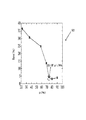
Cu支援エッチング方法の開発中、ある品質又は望ましいAR又はテクスチャー加工されたSi表面を得る為に有用な幾つかの要因又はプロセスパラメーターを特定した。エッチングプロセス中、ロー(ρ)として定義されるフッ化水素酸(HF)対過酸化水素(H2O2)のモル濃度の比を制御することが好ましく、ρは、HFのモル濃度をHF及びH2O2のモル濃度の合計で割ったものに等しい(即ち、ρ=[HF]/([HF]+[H2O2])。ρが約70パーセントを超え、HFの体積濃度が10パーセント以上(場合による)であり、HF及びH2O2が高濃度であり、水での希釈がわずかであるCu支援エッチングによって、74パーセント以上のρで、スペクトルで重み付けされた反射が約3パーセントとなる。比較として、Au支援エッチングでは、p約36パーセントのρが必要となる場合があり、Ag支援エッチングでは約92パーセントのρが必要となる場合がある。 During development of the Cu assisted etching method, several factors or process parameters were identified that were useful for obtaining a certain quality or desirable AR or textured Si surface. During the etching process, it is preferred to control the molar concentration ratio of hydrofluoric acid (HF) to hydrogen peroxide (H 2 O 2 ), defined as rho (ρ), where ρ is the molar concentration of HF And equal to the sum of the molar concentrations of H 2 O 2 (ie, ρ = [HF] / ([HF] + [H 2 O 2 ]), where ρ is greater than about 70 percent and the volume concentration of HF Cu-assisted etching with 10% or more (optional), high HF and H 2 O 2 concentration, and slight dilution with water results in spectrally weighted reflections at ρ of 74% or more For comparison, Au assisted etching may require p of about 36 percent ρ, and Ag assisted etching may require about 92 percent ρ.
Cu支援エッチングは、エッチング混合物が水であまり希釈されないことを保証する為に、濃縮されたHF及びH2O2を使用することによっても改善又は促進される。更に、エッチングステップの前にSi表面上に得られるCuナノ粒子対間隔の比(サイズ/間隔)を制御することが通常は望ましい。Cuナノ粒子サイズ及び間隔によって、Cu支援エッチングを用いて形成されたナノポーラスSi構造の構成が決定され、その結果として低反射率が得られる。例示的であるが非限定的な一例において、Si基板上に有用なARコーティングを実現する為に、Cuナノ粒子サイズは、少なくとも約20nmとなるように選択し、間隔は少なくとも約5nmとなるように選択した(例えば、サイズ対間隔の比が少なくとも約4)。これらのパラメーター/要因を制御することで、シリコン基板の作製にCu支援ナノポーラス黒色Siエッチングを使用して、太陽電池を容易に製造することができる。例えば、高効率太陽電池は、拡散接合エミッタを含むCu系ナノポーラス黒色シリコンを使用することによって、容易に得ることができる。 Cu assisted etching is also improved or facilitated by using concentrated HF and H 2 O 2 to ensure that the etching mixture is not significantly diluted with water. Furthermore, it is usually desirable to control the ratio (size / spacing) of Cu nanoparticles to spacing obtained on the Si surface prior to the etching step. The Cu nanoparticle size and spacing determine the configuration of the nanoporous Si structure formed using Cu assisted etching, resulting in low reflectivity. In an exemplary but non-limiting example, to achieve a useful AR coating on a Si substrate, the Cu nanoparticle size is selected to be at least about 20 nm and the spacing is at least about 5 nm. (Eg, a size to spacing ratio of at least about 4). By controlling these parameters / factors, it is possible to easily manufacture solar cells using Cu-assisted nanoporous black Si etching for silicon substrate fabrication. For example, a high-efficiency solar cell can be easily obtained by using Cu-based nanoporous black silicon including a diffusion junction emitter.
或る用途では、ナノポーラスSiをエッチングする為の金属としてのCuの使用は、Ag又はAuの使用に対して利点を有する。CuはAg及びAuよりもはるかに安価である。更に、Cuは、商業的なSi微細加工施設において既に広範に使用されている金属であるので、本明細書に記載のエッチングプロセスにおけるその更なる使用は、既存の工業技術に適合すると思われる。テクスチャー加工されたSi基板を太陽電池に使用する前に、硝酸洗浄を使用することで、銅ナノ粒子を容易に溶解させて除去することができる。更に、Si系太陽電池に関連する研究では、シリコン中のCu不純物は、Au及びAgよりもSi太陽電池性能に対する悪影響が少ないことが分かっており、その為、エッチングによって導入される全ての残留Cu不純物をナノポーラスSi表面から除去する為のポストエッチング処理は、所望のSi基板を得る為には、Au及びAg不純物の除去の除去ほどには重要ではない。 In some applications, the use of Cu as a metal for etching nanoporous Si has advantages over the use of Ag or Au. Cu is much cheaper than Ag and Au. Furthermore, since Cu is a metal already widely used in commercial Si microfabrication facilities, its further use in the etching process described herein appears to be compatible with existing industrial technology. By using nitric acid cleaning before using the textured Si substrate for solar cells, the copper nanoparticles can be easily dissolved and removed. In addition, studies related to Si-based solar cells have shown that Cu impurities in silicon have less adverse effects on Si solar cell performance than Au and Ag, and therefore any residual Cu introduced by etching. The post-etching process for removing impurities from the nanoporous Si surface is not as important as the removal of Au and Ag impurities in order to obtain a desired Si substrate.
このようなCu支援用途では、シリコン表面をテクスチャー加工する方法を提供することができる。この方法は、シリコン表面を有する基板を容器中に入れるステップを含むことができ、シリコン表面には、複数の堆積された銅粒子又は銅粒子のコーティングが付着しているが、表面を完全には覆わない。この方法は、基板のシリコン表面を覆う体積のエッチング溶液を溶液に満たすステップを更に含むことができる。エッチング溶液は、エッチング剤とケイ素酸化剤とを含む酸化剤−エッチャント溶液を含むことができる。この方法は、容器中のエッチング溶液を撹拌(例えば、超音波撹拌又は音波処理)することによってシリコン表面をエッチングするステップを更に含むことができる。 In such Cu support application, a method for texturing a silicon surface can be provided. The method can include placing a substrate having a silicon surface into a container, the silicon surface having a plurality of deposited copper particles or a coating of copper particles attached thereto, but the surface being completely Do not cover. The method may further comprise filling the solution with a volume of etching solution covering the silicon surface of the substrate. The etching solution can include an oxidant-etchant solution that includes an etchant and a silicon oxidant. The method can further include etching the silicon surface by agitating (eg, sonicating or sonicating) the etching solution in the container.
場合によっては、この方法は、エッチング容器中に基板を入れるステップの前に、シリコン表面上に銅粒子を堆積する為に無電解析出を行うステップを含むことができる。この堆積は、銅粒子が約28nm未満(約20nm等)のサイズを有するように行うことができ、無電解析出は、シリコン表面上の粒子サイズ対粒子間隔の比が3〜5の範囲内(例えば、Cuが20nmの粒子として得られる場合は間隔が5nm)となるように、更に実施/制御することができる。無電解析出を行うことで、3〜8ナノメートルの範囲内のシリコン表面上の粒子間隔を得ることができる。エッチング剤(例えば、HF)の濃度は、エッチング溶液の全体積の少なくとも約10パーセントであってよく、一方、酸化剤(例えば、H2O2)の濃度は少なくとも約2パーセントである。 In some cases, the method can include performing electroless deposition to deposit copper particles on the silicon surface prior to placing the substrate in the etch vessel. This deposition can be performed such that the copper particles have a size of less than about 28 nm (such as about 20 nm), and electroless deposition can be performed with a ratio of particle size to particle spacing on the silicon surface in the range of 3-5 ( For example, when Cu is obtained as particles of 20 nm, it can be further implemented / controlled so that the interval is 5 nm). By performing electroless deposition, particle spacing on the silicon surface in the range of 3-8 nanometers can be obtained. The concentration of the etchant (eg, HF) can be at least about 10 percent of the total volume of the etch solution, while the concentration of the oxidant (eg, H 2 O 2 ) is at least about 2 percent.
或るテクスチャー加工方法では、エッチングは、エッチングされたシリコン表面が、約350〜約1000ナノメートルの波長範囲において約5パーセント未満の反射率を有するまで行われる(例えば、試験の場合ではCu支援エッチングで約3パーセントが得られる)。一部の実施では、HFをエッチング剤として使用し、H2O2、O3、CO2、K2Cr2O7、CrO3、KIO3、KBrO3、NaNO3、HNO3、及びKMnO4の1つを使用することができる。例えば、ケイ素酸化剤はH2O2であってよく、エッチング溶液が少なくとも約70パーセントのロー(ρ)値を有する場合に、望ましいテクスチャー加工が実現され、ここでρは、HFのモル濃度をHF及びH2O2のモル濃度の合計で割ったものとして定義される。場合によっては、シリコン表面のエッチング中、エッチング溶液は30〜50℃の範囲内の温度に加熱され、約200ナノメートルを超え(典型的には約500ナノメートル未満)の深さを有する複数のトンネルがエッチングによってシリコン表面中に形成されるように選択された長さの時間にわたってエッチングを行うことができる。 In some texturing methods, etching is performed until the etched silicon surface has a reflectivity of less than about 5 percent in the wavelength range of about 350 to about 1000 nanometers (eg, Cu assisted etching in the case of testing). Gives about 3 percent). In some implementations, HF is used as an etchant and H 2 O 2 , O 3 , CO 2 , K 2 Cr 2 O 7 , CrO 3 , KIO 3 , KBrO 3 , NaNO 3 , HNO 3 , and KMnO 4. One of these can be used. For example, the silicon oxidizer may be H 2 O 2 and desirable texturing is achieved when the etching solution has a low (ρ) value of at least about 70 percent, where ρ is the molar concentration of HF. It is defined as divided by the sum of the molar concentrations of HF and H 2 O 2. In some cases, during etching of the silicon surface, the etching solution is heated to a temperature in the range of 30-50 ° C. and has a plurality of depths greater than about 200 nanometers (typically less than about 500 nanometers). The etching can be performed for a selected length of time such that a tunnel is formed in the silicon surface by etching.
上記の例示的な態及び実施形態に加えて、更なる態様及び実施形態は、図面を参照し以下の説明を検討することによって明らかとなるであろう。 In addition to the exemplary aspects and embodiments described above, further aspects and embodiments will become apparent by reference to the drawings and by considering the following description.
図面中の参考図において代表的な実施形態を示す。本明細書において開示される実施形態及び図面は、限定ではなく実例と見なされることを意図している。 A representative embodiment is shown in a reference view in the drawings. The embodiments and figures disclosed herein are intended to be considered illustrative rather than limiting.
反射率を大きく低下させる為の密度勾配のある表面の形成(例えば、太陽電池に使用できるシリコンウエハ上への反射防止面の形成)等の為にシリコン表面のエッチング又はテクスチャー加工を行う代表的な方法及びシステムを以下に説明する。最初に、図1〜7に参照されるエッチング又はテクスチャー加工の方法を補助する金又は銀のナノ粒子を提供する触媒金属源を使用することによる、これらの方法及びシステムを説明する。 Typical etching or texturing of the silicon surface for the formation of a surface with a density gradient to greatly reduce the reflectivity (for example, the formation of an antireflection surface on a silicon wafer that can be used in solar cells). The method and system are described below. First, these methods and systems are described by using a catalytic metal source that provides gold or silver nanoparticles to assist the etching or texturing method referenced in FIGS.
この議論の次に、シリコンの反射防止エッチングを行う為の金属支援化学作用を提供する別の方法が続けられる。発明の概要の項の終盤で前述したように、Cuナノ粒子を使用してシリコン基板を効率的にエッチングすることができ、無電解Cu堆積を用いたCu支援エッチングによって、低反射率(例えば、約5パーセント未満、例えば約3パーセント)のナノポーラス又はテクスチャー加工されたSi基板表面を得ることが可能なことが分かった。この研究以前では、当技術分野の多くでは、金及び銀等の金属と比較すると銅は熱力学的に望ましくないと考えられていたので、銅はそのような使用には望ましくないと見なされていた。本明細書に記載のエッチング条件とは異なる条件で銅を用いた従来の金属支援エッチングでは、低反射率面は得られていない。 This discussion is followed by another method of providing a metal assisted chemistry for performing an antireflective etch of silicon. As mentioned earlier in the summary section of the invention, Cu nanoparticles can be used to efficiently etch a silicon substrate, and Cu assisted etching using electroless Cu deposition can reduce low reflectivity (eg, It has been found that it is possible to obtain nanoporous or textured Si substrate surfaces of less than about 5 percent (eg, about 3 percent). Prior to this study, copper was considered undesirable for such use because much of the art considered copper to be thermodynamically undesirable compared to metals such as gold and silver. It was. In conventional metal assisted etching using copper under conditions different from the etching conditions described herein, a low reflectivity surface has not been obtained.
ナノポーラス黒色Siを得るにはCuを有効に使用できないと予想されていたことから、反射防止面を得る為のSiのCu系ナノポーラスエッチングの為に、他の者は、銅を使用しその化学作用を開発することを思いとどまっていた。反射防止面を形成する為にCuを使用する場合、最初に、このような予測及び理解にもかかわらず、シリコンのエッチングを行う為の金属化学に銅ナノ粒子が有用となり得ることを認識する必要があった。しかし、有用な金属化学及びCu支援エッチングプロセスの開発は簡単ではなく、本出願人らの系統的な研究によってのみ実現することができ、そのことがCu系ナノポーラス黒色Siを得る為の代表的な化学作用の決定に役立った。 Since it was expected that Cu could not be used effectively to obtain nanoporous black Si, other people used copper for its Cu-based nanoporous etching to obtain an antireflection surface, and its chemical action. I was stuck with developing. When using Cu to form an anti-reflective surface, it is first necessary to recognize that copper nanoparticles can be useful in metal chemistry for etching silicon, despite such prediction and understanding was there. However, the development of useful metal chemistry and Cu assisted etching processes is not simple and can be realized only by the systematic research of the applicants, which is a representative for obtaining Cu-based nanoporous black Si. Helped determine the chemistry.
Cu支援エッチングの実験において、過酸化水素(H2O2)、フッ化水素酸(HF)、及び脱イオン水(H2O)の種々の組み合わせを、ρ、HF、及びH2O2の体積濃度に関して試験した。例えば、或る一連の試験では、H2O2の体積を1.5mlに維持又は設定し、H2Oの体積を50mlに設定し、次にHFの体積を0.25ml(ρ≒22%、全体積の0.5%のHF、全体積の3%のH2O2)〜8ml(ρ≒90%、全体積の14%のHF、及び全体積の2.5%のH2O2)まで変化させた。Cuナノ粒子は、HFで清浄にした平面上(100)p型浮遊帯(FZ)Si基板上に1分間無電解析出させた(例えば、(非特許文献1)に示されるような方法を使用)。Cuナノ粒子で覆われた試料を次に、50℃のH2O2:HF:H2O溶液中に、溶液の撹拌を続けながら5分間入れた。この試験において、74%≦ρ≦90%、5%≦HF%体積、及び1%≦H2O2%体積≦3%の場合、スペクトルで重み付けされた反射Raveは、3〜4%の範囲内のままであった。この反射率の結果は、比較的良好な反射防止面(又はSi基板)が得られ、Ag又はAuの触媒を用いて得られる結果と同等である。ナノポーラスSiのSEM(走査電子顕微鏡)分析は、HF濃度が増加すると細孔密度及び深さが増加し、その結果、ある機構によって十分な密度グレードが得られることを示唆している。 In Cu-assisted etching experiments, various combinations of hydrogen peroxide (H 2 O 2 ), hydrofluoric acid (HF), and deionized water (H 2 O) were used for ρ, HF, and H 2 O 2 . Tested for volume concentration. For example, in one series of tests, the volume of H 2 O 2 is maintained or set at 1.5 ml, the volume of H 2 O is set at 50 ml, and then the volume of HF is 0.25 ml (ρ≈22% , 0.5% HF of the total volume, 3% H 2 O 2 of the total volume) to 8 ml (ρ≈90%, 14% HF of the total volume, and 2.5% H 2 O of the total volume. 2 ). Cu nanoparticles were electrolessly deposited on a (100) p-type floating zone (FZ) Si substrate on a flat surface cleaned with HF for 1 minute (for example, using a method as shown in (Non-patent Document 1)). ). The sample covered with Cu nanoparticles was then placed in a 50 ° C. H 2 O 2 : HF: H 2 O solution for 5 minutes with continued stirring of the solution. In this test, when 74% ≦ ρ ≦ 90%, 5% ≦ HF% volume, and 1% ≦ H 2 O 2 % volume ≦ 3%, the spectrally weighted reflection R ave is 3-4%. Remained in range. This reflectivity result is comparable to that obtained using a Ag or Au catalyst, with a relatively good antireflection surface (or Si substrate) being obtained. SEM (scanning electron microscopy) analysis of nanoporous Si suggests that increasing HF concentration increases pore density and depth, resulting in a sufficient density grade by some mechanism.
ここで、最初に金及び銀に関して、エッチング方法は、酸化剤−エッチャント溶液(例えば、エッチング剤及び酸化剤、例えばHF及びH2O2の水溶液)と、触媒金属を含有する分子又はイオン種の供給源(例えば、エッチング溶液中に金を供給する為の水溶液中の塩化金酸等の酸、又は銀を提供する為の水溶液中のAgF等)とで構成される或る堆積のエッチング溶液中にシリコン表面を配置するステップを含む。エッチング溶液の浴又は体積は、シリコン表面のテクスチャー加工が所望の量/深さで実現されるまで、或る時間(又はあるエッチング時間)の間かき混ぜ又は撹拌が行われ、これによって、シリコン表面上に非反射性層又はテクスチャー加工された層が形成されたと見なすことができる。次に、金又は別の金属触媒がシリコン表面から洗浄又は除去され、次にシリコン表面、或いはそのような表面を有するウエハ又は基板を使用して、太陽電池、生物医学装置、光電気部品等のデバイスを製造することができる。 Here, initially with respect to gold and silver, the etching method includes an oxidant-etchant solution (eg, an etchant and an oxidant, eg, an aqueous solution of HF and H 2 O 2 ), and a molecular or ionic species containing a catalytic metal In an etching solution of some deposition comprised of a source (eg an acid such as chloroauric acid in an aqueous solution to supply gold into the etching solution, or AgF in an aqueous solution to provide silver) Placing a silicon surface on the substrate. The bath or volume of the etching solution is agitated or agitated for a period of time (or an etching time) until the texturing of the silicon surface is achieved in the desired amount / depth, so that It can be considered that a non-reflective layer or a textured layer is formed. Next, gold or another metal catalyst is cleaned or removed from the silicon surface, and then using the silicon surface, or a wafer or substrate having such a surface, such as solar cells, biomedical devices, optoelectronic components, etc. Devices can be manufactured.
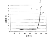
本明細書に記載のエッチング方法は、安価な化学物質(例えば、酸化剤−エッチャント溶液中の金、白金、銀、又は他の触媒金属の触媒量のイオン又は分子の化合物形態に基づく反応は、非常に安価で行われる)を使用できるシリコンのエッチングの為の溶液に基づく方法を提供する。このエッチング方法は、エッチングが、酸化剤−エッチャント溶液及び金属イオン又は金属分子溶液の存在下、それらの超音波又は他の撹拌の影響下で行われるという意味で、「多段階」ではなく「1段階」である。このエッチング方法は、部分的にはその単純さ及び速度の為に好都合であり、エッチング時間は比較的短く、エッチング前の堆積/コーティングが不要である。このエッチング方法は、広いスペクトルにわたって低反射率であるテクスチャー加工されたシリコン表面が得られることでも望ましく、これらの非反射性層又はテクスチャー加工されたシリコン表面は、反射防止に関して広い受光角を有する。更に、このエッチング方法は、多結晶シリコンを含むほぼ全てのシリコン表面に適用できる。示されるように、結果として得られるシリコン表面は、光起電力又は太陽電池産業において非常に望ましいと思われる。例えば、触媒溶液として又はその一部としてHAuCl4が使用されるエッチング方法が、400nmの波長における約0.3%から1000nmの波長における約2.5%の範囲の反射率を有し、有用な太陽スペクトルの大部分で1%未満の反射率である<1,0,0>結晶シリコンウエハに対して使用されている。触媒溶液がAgFを含んだ場合、このエッチング溶液技術によって、100結晶シリコンウエハ上で約5%未満の反射を得ることができた。 The etching methods described herein are based on inexpensive chemicals (e.g., reactions based on catalytic forms of ionic or molecular compound forms of gold, platinum, silver, or other catalytic metals in oxidant-etchant solutions) It provides a solution based method for etching silicon that can be used at a very low cost. This etching method is “1” rather than “multi-step” in the sense that the etching is performed in the presence of an oxidant-etchant solution and a metal ion or metal molecule solution under the influence of their ultrasound or other agitation. Stage. This etching method is advantageous in part because of its simplicity and speed, etching time is relatively short, and no pre-etching deposition / coating is required. This etching method is also desirable to obtain textured silicon surfaces that are low reflectance over a broad spectrum, and these non-reflective layers or textured silicon surfaces have a wide acceptance angle with respect to antireflection. Furthermore, this etching method can be applied to almost all silicon surfaces including polycrystalline silicon. As shown, the resulting silicon surface appears highly desirable in the photovoltaic or solar cell industry. For example, an etching method in which HAuCl 4 is used as or as part of a catalyst solution has a reflectance in the range of about 0.3% at a wavelength of 400 nm to about 2.5% at a wavelength of 1000 nm, and is useful. Used for <1,0,0> crystalline silicon wafers with reflectivity of less than 1% in the majority of the solar spectrum. When the catalyst solution contained AgF, this etch solution technique was able to obtain less than about 5% reflection on a 100 crystal silicon wafer.
明らかとなるように、本発明のエッチング方法を実施する為に、多数の触媒溶液又は触媒金属源を使用することができる。一実施形態では、金の分子又はイオン種が得られる触媒溶液(例えば、水溶液中の塩化金酸(HAuCl4))が使用されるが、別の代表的な実施形態では、銀の分子又はイオン種が得られる触媒溶液(例えば、AgFを有する溶液)が使用される。一般に、分子又はイオン種又はそのような触媒を含有する触媒溶液は、HF等のエッチャント、及び更にはH2O2等の酸化剤と混合される。別の実施形態においては、触媒溶液は、白金等のエッチング溶液中の遷移金属及び/又は貴金属等の別の金属の分子及び/又はイオン種が得られるように選択することができ、このことは、エッチングの費用を更に削減するのに有用となることがあり、金よりも悪影響の少ない不純物をシリコン中に有し得るので望ましい場合がある。 As will be apparent, a number of catalyst solutions or catalyst metal sources can be used to carry out the etching method of the present invention. In one embodiment, a catalyst solution that yields gold molecules or ionic species (eg, chloroauric acid (HAuCl 4 ) in aqueous solution) is used, while in another exemplary embodiment, silver molecules or ions A catalyst solution from which a seed is obtained (eg a solution with AgF) is used. In general, a molecular or ionic species or catalyst solution containing such a catalyst is mixed with an etchant such as HF and further an oxidizing agent such as H 2 O 2 . In another embodiment, the catalyst solution can be selected to obtain molecules and / or ionic species of another metal such as a transition metal and / or noble metal in an etching solution such as platinum. It may be useful to further reduce the cost of etching, and may be desirable because it can have impurities in silicon that are less harmful than gold.
一般に、シリコン表面は研磨された表面であるが、場合によっては、エッチング技術は、別の反射防止技術と組み合わせて実施することができる。例えば、シリコン表面は、異方性の角錐型にテクスチャー加工されたSi<1,0,0>表面(又は他のテクスチャー加工が行われたSi表面)であってよく、これは次に、Si<1,0,0>表面(又はSi表面/層を有する基板/ウエハ/デバイス)を、触媒溶液(触媒金属の金属含有分子又はイオン種を有する)と、エッチング剤と、酸化剤とを含むエッチング溶液中に配置することによる1段階のエッチングプロセスで処理される。独立して使用される場合、又は別の表面仕上げ方法と併用される場合、エッチング溶液は、超音波撹拌又は音波処理等を用いて或る時間(例えば、あらかじめ決定されたエッチング時間)かき混ぜ又は撹拌が行われる。 In general, the silicon surface is a polished surface, but in some cases the etching technique can be performed in combination with another anti-reflection technique. For example, the silicon surface may be a Si <1,0,0> surface textured in an anisotropic pyramid shape (or other textured Si surface), which is then Si <1,0,0> surface (or substrate / wafer / device having Si surface / layer), containing catalyst solution (having metal-containing molecule or ionic species of catalyst metal), etching agent, and oxidizing agent It is processed in a one-step etching process by placing it in an etching solution. When used independently or in combination with another surface finishing method, the etching solution is stirred or stirred for a period of time (eg, a predetermined etching time) using ultrasonic agitation or sonication or the like. Is done.
以下の説明は、反射率の制御(即ち、減少又は最小化)に使用する為の、シリコン表面のエッチングにおける触媒溶液の使用を重点に置いているが、本明細書に記載のエッチング技術は、光電子デバイス、生物医学装置等の特定の表面粗さ又は平滑ではないトポロジーを有するシリコン表面が得られることが望ましいほぼ全ての用途の為の、シリコンのテクスチャー加工に使用することができる。説明は、図1〜3を参照してエッチング方法の概要から始められる。次に図4が参照され、説明では、説明されるテクスチャー加工方法によって形成された反射防止面を有するシリコン基板又はウエハを用いて形成できるデバイスの一例、即ち太陽電池が提供される。次に、説明では、特に太陽電池の効率を増加させる(例えば、シリコンの光起電力デバイス中のフォトンの吸収を増加させる)為に反射率を低下させる又はほぼなくすのに有用な結果を得る為の、代表的な処方(例えば、触媒溶液及びこれらの溶液を得ることができる触媒金属、エッチング剤、酸化剤、シリコン表面、撹拌方法、エッチング時間等の比率及び個別の種類)、プロセス等の議論を提供する。 The following description focuses on the use of a catalyst solution in etching the silicon surface for use in reflectance control (ie, reduction or minimization), but the etching techniques described herein include: It can be used for silicon texturing for almost any application where it is desirable to obtain silicon surfaces with a specific surface roughness or non-smooth topology, such as optoelectronic devices, biomedical devices and the like. The description begins with an overview of the etching method with reference to FIGS. Referring now to FIG. 4, the description provides an example of a device that can be formed using a silicon substrate or wafer having an anti-reflective surface formed by the described texturing method, ie, a solar cell. Next, the description will give results useful to reduce or substantially eliminate reflectivity, especially to increase solar cell efficiency (eg, increase photon absorption in silicon photovoltaic devices). Of typical formulations (eg, catalyst solutions and catalyst metals that can be used to obtain these solutions, etching agents, oxidizing agents, silicon surfaces, ratios of stirring methods, etching times, etc., and individual types), discussion of processes, etc. I will provide a.
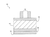
図1は、一実施形態のテクスチャー加工又はエッチングのシステム100を示している。システム100は、シリコン表面を有する或る量のウエハ、基板、又はデバイス110又はそれらの供給源を含む。これらは、太陽電池、オプトエレクトロニクス、又は他の製品に使用されるべきSiウエハであってよい。シリコン試料112上のシリコン表面116は、単結晶、多結晶、非晶質等であってよく、ドーピングの種類は、種々の量(例えば約0.25Ωcm〜約50Ωcm等)のn型又はp型のドーピングとなるように変化させることができる。ウエハ、基板、又はデバイス110は、システム100の操作中にエッチングされる1つのシリコン表面、又は2つ以上のそのような表面を有することができる。システム100は、金属堆積ステーションは不要であるが、その代わりにシステム100は、ウェットエッチング容器又はコンテナ122を有するエッチング組立体120を含む。操作中、ある体積のエッチング溶液124を加える前又は後に、1つ以上のSiウエハ110又は基板112上のSi層を容器122中に入れる。図1中、1つの基板112が容器中にシリコン表面116を露出されて示されているが、当然ながら複数のこのような表面116を同時にエッチングすることができる。
FIG. 1 illustrates a texturing or
組立体120は、最初に及び/又はエッチング中に溶液124を撹拌又はかき混ぜる為の機構126を含む。機構126は、機械的又は磁気的な撹拌装置であってよいが、場合によっては、反応物又はエッチング溶液124等の溶液の音波処理によるかき混ぜ/撹拌の為に超音波撹拌機を使用すると、より強化された又はより繰り返し可能な結果が得られる。組立体120は、表面116のエッチングを促進する1つ以上の所望の温度範囲内でエッチング溶液124の温度を維持又は上昇させる為のヒーター128を含むことができる。溶液の温度を監視する為に温度ゲージ又は温度計130を設けることができ(任意選択で、制御フィードバック信号をヒーター128に送ることができ)、エッチング又はストリッピングステップに関して組立体120の操作者に視覚的及び/又は音声的指示を提供する為にタイマー134を使用することができる。
The assembly 120 includes a
システム100は、触媒金属の金属含有分子又はイオン種等の触媒金属を供給する又は供給源となる触媒溶液140を更に含む。この供給源は、金、銀、白金、パラジウム、銅、ニッケル、コバルト等の或る量の遷移金属又は貴金属等の或る量の触媒をエッチング溶液124に供給する。良好な結果は、通常、容器122中のエッチング溶液124中の酸化剤−エッチャント溶液と混合した場合に、そのような金属の金属含有分子又はイオン種を放出する、HAuCl4、AgF、及び類似の酸又は材料を含有する溶液を用いて実現される。一般に、金属触媒を有するこの触媒溶液は、容器122に加えられてエッチング溶液124の一部を構成するが、別の場合では、この溶液(或いは触媒金属の金属含有分子又はイオン種の別の供給源)140は、Si基板112が入れられた容器122に加えられる前に、最初に酸化剤−エッチャント溶液146(又はその成分142、144の1つ)に加えられる。具体的な触媒溶液及びそれらの構成は、以下に更に詳細に議論する。
The
シリコン表面116のエッチングを実現する為に、システム100は、元のエッチング剤142と酸化剤144とを含む。これらは特にシリコンのテクスチャー加工/エッチングの為に選択され、エッチング剤142は、HF、NH4F、又は類似のエッチャントであってよい。酸化剤は、H2O2であっても、触媒溶液140によって供給される金属によって分解が触媒されるもの等の別の物質であってもよい。例えば、酸化剤144としては、H2O2、O3、CO2、K2Cr2O7、CrO3、KIO3、KBrO3、NaNO3、HNO3、KMnO4等、又はそれらの混合物を挙げることができる。これらの物質(又はそれらの溶液)142、144は、別々に容器122に加えて触媒溶液140とともにエッチング溶液124を形成することも、図示されるように、最初にエッチング剤142と酸化剤144とを1つにまとめることによって酸化剤−エッチャント溶液146を形成し、次にこの溶液を容器122に入れることもできる。次に組立体120に対して、機構126による撹拌及びヒーター128による加熱等の操作を或る時間(「エッチング時間」)行って、表面116のテクスチャー加工を行う。エッチング時間の経過後、溶液124を除去し(又は基板112を金属ストリッピング用の別のコンテナ又は容器に移動させ)、シリコン中に望ましくない不純物が存在する可能性があるので、残存する金属触媒を除去する。この目的の為、システム100は、容器122に加えられる金属ストリッピング溶液150の供給源を含み、溶液140の全て又は実質的に全ての金属が表面116から除去されるまで、機構126によってストリッピング溶液のかき混ぜ又は撹拌(及び、任意選択でヒーター128による加熱)を行うことができる。次に、基板又はウエハ112は、そのまま使用することも、太陽電池又は光起電力デバイス、光電気デバイス、生物医学装置等のより大型のデバイスの部品又は層として使用することもできる。
In order to achieve the etching of the
図2は、本明細書に記載のエッチングプロセスの処理後のシリコンウエハ200を示している。図示されるように、ウエハ200は、或る時間又は或るエッチング時間の間だけエッチング溶液に曝露した上面又はSi表面210を含む。Si表面210は、反射率が大幅に低下したナノスケールの粗面仕上げを有する。重要なことには、本明細書に記載の触媒溶液の使用によって、その場で又はエッチング溶液中で金、銀、又は別の金属のナノ粒子(触媒溶液の構成に依存して例えば2〜30nmの金粒子、2〜30nmの銀粒子等)を生成する機能を果たし、それによって表面210が複数のピット又はトンネル214を有するようになると考えられ、エッチングはナノ粒子(図2には示されていない)が存在することでより迅速に進行する。触媒溶液と酸化剤−エッチャント溶液との併用によって実現されるエッチング結果は、完全に又は部分的に別の機構が原因である場合がある。作用する機構に関わらず、各トンネル214は、直径DiamTunnelと、通常は約300マイクロメートルであるウエハ200の厚さtwaferよりも小さい(例えば、最大約99.91%小さい)深さDTunnelとを有する開口部216を表面210に含む。例えば、トンネル直径DiamTunnelは、粒子サイズよりもある程度大きくなる場合があり、例えば、5〜10nmのナノ粒子がエッチング溶液中に存在する場合に約21〜約23nmとなり得る。トンネル深さDTunnelは、所望の物理的性質(例えば、反射との干渉)が得られるように選択することができる。シリコン層210によって反射率を制御する場合、トンネル深さDTunnelは、約50〜約300nmの間であってよい(例えば、或る試験では250〜280nmの深さ範囲のトンネルが有用であることが示された)。実際には、所望の深さは、個々のエッチング溶液の時間及び温度を制御することによって選択又は実現される。図2から分かるように、触媒金属(及び、任意選択で、そのような金属のナノ粒子)の供給源となる触媒溶液を伴うエッチングプロセスは、勾配のある密度でナノスケールの粗さ又は構造を得るのに有効であり、このことは反射率の低下の為に望ましい。
FIG. 2 shows the
図3は、限定するものではないが、反射率を低下させる、又は黒色表面を形成するテーパー付き表面等の所望の特性を得る為にシリコン表面を処理する為の溶液系エッチング又はテクスチャー加工方法300の一実施形態を示している。方法300は、テクスチャー加工されるシリコン表面の種類、例えば、シリコンウエハ、或いはシリコン層及びシリコン表面を有する基板又はデバイス、特定の結晶表面又は構成、並びに特定のドーピングの種類の計画又は選択等を行う305から開始する。ステップ305は、シリコン表面のテクスチャー加工又はエッチングの処方又は段階的計画の選択を含むこともでき、触媒金属、並びにそのような金属の分子又はイオン種の供給源、シリコン表面のエッチング剤(例えば、HF等)及び酸化剤(例えば、H2O2、O3、CO2、K2Cr2O7等)、これら2つの成分を含む酸化剤−エッチャント溶液を得る為のこれらのそれぞれの比率、撹拌/かき混ぜの種類及び量、エッチングで得られる表面貫入の所望の深さ、並びにエッチングの時間及び温度(当然ながら、これらは前の決定/パラメーターによって変動する)の選択を含むことができる。
FIG. 3 illustrates, but is not limited to, a solution-based etching or
テクスチャー加工/エッチング方法300は続いて、シリコン表面を有するウエハ(又は基板/デバイス)を選択し、次に反応又はエッチング容器中に配置する310が行われる。320では、選択されたエッチング剤及び酸化剤(又はそれらの溶液)を組み合わせる又は混合することによって酸化剤−エッチャント溶液が形成されるが、或る実施形態においては、このステップは行われず、これら2つの物質は単に容器に同時又はほぼ同時に加えられる。方法300は、続いてステップ330及び340が実施され、これらは同時に行うことも、あらかじめ設定された時間内(例えば、各ステップの実施の間が約5分未満、又はより典型的には約2分未満)等のほぼ同時に行うこともでき、どちらを最初に行ってもよい。330において、酸化剤−エッチャント溶液をシリコン表面の入った容器中に加え又は投入し、340において、触媒溶液(金、銀、白金、パラジウム、銅、コバルト、ニッケル、別の貴金属又は遷移金属、或いは別の触媒金属/材料を含有する分子(又はそれらのイオン種)の供給源として機能する酸又は酸の水溶液等)を容器に加える。場合によっては、粒子は「乾燥」又は類似の形態で提供され、一方、別の場合では金属含有分子(又は酸化剤−エッチャント溶液の存在下でそのような分子又はイオン種が得られる材料)が脱イオン水又は水溶液中に含まれ、ある体積のそのような溶液が340において容器に加えられる。
The texturing /
350において、方法300は、機械的混合装置、又はより典型的には超音波混合技術又は音波処理等を用いて、容器中のエッチング溶液を混合又は撹拌するステップを含む。360において、方法300は、任意選択で、エッチングプロセスを促進する為に選択された所定の温度範囲に容器中の溶液を加熱する(又は酸化剤−エッチャント溶液の初期温度を所望の温度範囲に維持する為に加熱する)ステップを含むことができる。365において、方法300は、エッチング反応/プロセスを促進又は推進する為に、エッチング溶液及び/又はウエハ又はシリコン表面に光を照射するステップを含むことができる。例えば、高濃度でn型ドープされた表面等の特定のシリコン表面は、高強度の光の照射が好都合となる場合があり、それによってエッチング時間が短縮され得る(例えば、或る場合には8分以下までとなり、約5%未満の反射率まで等の向上した反射率結果が得られ、強い照射を使用しない場合では20〜30%が達成された)。370において、方法300は、あらかじめ設定されたエッチング時間(例えば、シリコン表面の種類、触媒金属、及び酸化剤−エッチャント溶液の組成に基づいて、所望の深さ又はエッチング量を得る為の試験によって前もって決定された時間)が経過したかどうかを決定するステップを含む。経過していない場合、方法300は350が続けられる。
At 350, the
370においてエッチング時間が経過した場合、方法300は、376においてエッチング溶液を容器から除去する、又はSiウエハを容器から取り出すステップを含む。380において、触媒溶液の組成に基づいて選択されたストリッピング溶液(例えば、金の場合、銀の場合、白金の場合等で、異なるストリッピング溶液を使用することができる)を使用する等によって、新しくテクスチャー加工されたシリコン表面から触媒金属を除去する。388において、方法300は、太陽電池、生物医学装置、光電気デバイス、消費者用電子デバイス等の、テクスチャー加工/エッチングが行われたシリコン表面を使用するデバイスを製造する為に、テクスチャー加工されたウエハを更に処理するステップを含むことができる。390において、方法300は終了する(同じ方法を繰り返すことができる場合、又は本明細書に記載の別の「処方」の1つを使用する等の為に変更できる場合にはステップ305に戻って繰り返される)。
If the etch time has elapsed at 370, the
前述したように、本明細書に記載の方法によりシリコン表面をエッチングすることが望ましくなり得る理由の1つは、全反射率がほとんど又は全くないシリコン系太陽電池の形成に使用されるシリコン基板が形成されることである(例えば、ARCの塗布や更なる処理が不要である)。ほぼあらゆる種類の太陽電池設計で、このエッチング方法を使用することができることが理解されるであろうし、本明細書の説明は、種々の設計の多種多様の太陽電池を扱うのに十分広くなることを意図している。しかし、現時点では、1つの有用で非限定的な太陽電池配列を少なくとも説明し、続いて1つの有用な製造技術について簡潔な議論を行うことが有用と思われ、次にこれらの説明は、本明細書に記載されるようにテクスチャー加工されたシリコン表面を有する太陽電池及び他のデバイスの製造に使用することができる。 As previously mentioned, one of the reasons that it may be desirable to etch the silicon surface by the methods described herein is that the silicon substrate used to form silicon-based solar cells with little or no total reflectivity. (For example, no application of ARC or further processing is required). It will be appreciated that this etch method can be used with almost any type of solar cell design, and the description herein will be broad enough to handle a wide variety of solar cells of different designs. Is intended. However, at present it seems useful to at least describe one useful, non-limiting solar cell arrangement, followed by a brief discussion of one useful manufacturing technique, It can be used in the manufacture of solar cells and other devices having a textured silicon surface as described in the specification.
図4は、比較的単純な太陽電池400を示している。図示されるように、この例示的な太陽電池400は、本明細書に記載の触媒ナノ材料系エッチング方法(図1のシステム100又は図3の方法300の使用等)を用いてテクスチャー加工又は粗面化された少なくとも1つの上面を有するシリコン基板410を含む。基板の反射率は、このような技術によって、約20パーセント未満、より典型的には約10パーセント未満、多くの場合では約0.3〜2.5パーセントの範囲内、又は最大約5パーセント以上になるように制御することができる。基板410は、例えば、ホウ素がドープされたp型シリコン、又は太陽電池に有用なほぼ全ての他のシリコン表面であってよい。このような場合、セル400は、シリコン基板410のテクスチャー加工された表面、即ち上面上に設けられたn型エミッタ層420を更に含むことができる。エミッタ層420の上に複数の電気接点(例えば、銀又は他の接点材料)430を配置することができ、セル400は、裏面電界層440(例えば、アルミニウム又は類似の金属の層)及び接触層450(例えば、アルミニウム又は類似の材料の層)等の所望の機能を付与する為の追加の層/部品を更に含むことができる。エッチングされた表面を有するシリコン基板410は、定形エッジ薄膜成長(edge−defined film fed grown)(EFG)シリコンウエハ、ストリングリボンシリコン、浮遊帯(FZ)シリコン、チョクラルスキー(CZ)成長シリコン、キャスト多結晶シリコン(mc−Si)、単結晶シリコン、エピタキシャル成長シリコン層、或いは別のシリコン構造又は種類等の多くの形態を取ることができる。
FIG. 4 shows a relatively simple
場合によっては、テクスチャー加工/エッチングされたシリコンウエハからの太陽電池の形成は、当業者に周知の引き続くプロセス又は別のプロセスを含むことができる。エミッタの形成は、エッチングされた表面を介する(例えば、スピンオンドーパントからの)燐又は類似の材料の拡散を含むことができる。ドーピング源は、濃HF中での更なるエッチング等で除去することができ、拡散の結果、n型領域を形成することができる。酸化(例えば、O2を使用)及びアニーリング(例えば、N2を使用)によって表面パッシベーションを行うことができ、これによって高濃度にドープされたエミッタにおける表面再結合を減少させる為にシリコンに対してアニールされた界面を有する乾燥酸化物層を得ることができる。次に、シリコンウエハ又は基板の裏面からパッシベーション酸化物を除去し、続いて真空蒸着等によってアルミニウム又は別の類似の金属の層と、銀又は類似の金属とをこれらの裏面表面上に取り付けることによって、裏面接点を形成することができる。続いて、ウエハ/基板の前面、即ちテクスチャー加工された表面側の上のパッシベーション酸化物中に多数のスリットを開け、次に真空蒸着及びフォトレジストのリフトオフ等によって、これらのスリットをTi等で覆うこと等によって、前面接点グリッドを形成することができる。太陽電池は、更なる加工、又は別のセルと組み合わせてソーラーモジュールを製造することができ、次にこれを連結して光起電力アレイを形成することができる。当然ながら、これは、太陽電池の簡略化された製造方法の1つに過ぎず、本明細書に記載の黒色エッチング表面を有するセルを形成する為に修正することも、当産業において周知の別の技術を代わりに使用することもできる。 In some cases, the formation of solar cells from textured / etched silicon wafers can include subsequent processes or other processes well known to those skilled in the art. Emitter formation can include diffusion of phosphorous or similar material (eg, from a spin-on dopant) through the etched surface. The doping source can be removed by further etching or the like in concentrated HF, and as a result of diffusion, an n-type region can be formed. Surface passivation can be performed by oxidation (eg, using O 2 ) and annealing (eg, using N 2 ), thereby reducing the surface recombination in heavily doped emitters relative to silicon. A dry oxide layer having an annealed interface can be obtained. Next, the passivation oxide is removed from the backside of the silicon wafer or substrate, followed by mounting a layer of aluminum or another similar metal and silver or similar metal on these backside surfaces, such as by vacuum evaporation. A back contact can be formed. Subsequently, a number of slits are opened in the passivation oxide on the front side of the wafer / substrate, i.e. on the textured surface side, and these slits are then covered with Ti etc. by vacuum evaporation, photoresist lift-off etc. For example, a front contact grid can be formed. The solar cells can be further processed, or combined with another cell to produce a solar module, which can then be joined to form a photovoltaic array. Of course, this is only one simplified method of manufacturing solar cells and can be modified to form cells having a black etched surface as described herein, which is another well known in the industry. The technology can be used instead.
本出願人らは、異なる触媒ナノ材料、酸化剤−エッチャント溶液、及びシリコン表面の種類/ドーピングを用いて多数の実験を行い、得られた表面の反射率についても試験した。以下の議論では、これらの実験、及び本出願人らの所見、並びにより一般的な結論及びそれらのアイデアの拡張を記載する。本明細書に記載の方法は、一般に、350〜1000nmの波長範囲内での反射率のほぼ完全な抑制を示すシリコン表面の製造に特に適した湿式化学方法である。本明細書に記載の方法は、単結晶p型チョクラルスキー、{<1,0,0,>及び<1,1,1,>}、n型及びp型浮遊帯、真性、nドープ、及びpドープ非晶質、並びにpドープ多結晶、並びに他のシリコン表面等の多くのシリコン基板を使用する場合に有用であると考えられる。 Applicants have conducted a number of experiments using different catalytic nanomaterials, oxidant-etchant solutions, and silicon surface types / dopings, and also tested the resulting surface reflectivity. The following discussion describes these experiments, and Applicants' findings, as well as more general conclusions and extensions of their ideas. The method described herein is generally a wet chemical method particularly suitable for the production of silicon surfaces that exhibit almost complete suppression of reflectivity within the wavelength range of 350-1000 nm. The methods described herein include single crystal p-type Czochralski, {<1,0,0,> and <1,1,1,>}, n-type and p-type floating zones, intrinsic, n-doped, And p-doped amorphous, as well as p-doped polycrystalline, and other silicon surfaces, are considered useful when using many silicon substrates.
或る組の実験においては、触媒溶液は、HAuCl4、AgF等の形態で存在し得る金、銀、白金、及び他のイオンの希薄(例えば、約2mM未満、又は或る場合では約1mM未満の)溶液であった。この触媒溶液を酸化剤−エッチャント溶液に加え、これらの溶液を撹拌下で混合して、シリコン表面をエッチングするエッチング溶液を形成する。最低達成可能反射率(例えば、約3%未満、例えば1〜2%又は更には金を触媒として使用する場合の等の一部の場合で0.2〜0.4%)を得て、比較的均一な表面テクスチャーも実現する為のエッチング時間は、約4分未満(例えば、2〜4分、又は同様の時間)等であり、従来のエッチング技術に対してはるかに短かった。このようなエッチング結果は、あらゆる方位の多結晶及び単結晶の両方のシリコンウエハで実現可能であることが分かった。更に、厚さ約1マイクロメートルの非晶質シリコン層は、最低達成可能反射率を達成するのにわずか約90秒しか必要としなかった。 In some sets of experiments, the catalyst solution is a dilute of gold, silver, platinum, and other ions that may be present in the form of HAuCl 4 , AgF, etc. (eg, less than about 2 mM, or in some cases less than about 1 mM). Solution). This catalyst solution is added to the oxidant-etchant solution and these solutions are mixed under stirring to form an etching solution that etches the silicon surface. Obtain and compare the minimum achievable reflectivity (e.g. less than about 3%, e.g. 1-2% or even 0.2-0.4% in some cases such as when gold is used as catalyst) The etch time to achieve a more uniform surface texture was less than about 4 minutes (eg, 2-4 minutes, or similar), and was much shorter than conventional etching techniques. It has been found that such etching results are feasible with both polycrystalline and single crystal silicon wafers of any orientation. Furthermore, an amorphous silicon layer about 1 micrometer thick required only about 90 seconds to achieve the lowest achievable reflectivity.
エッチングプロセス中の撹拌/かき混ぜに関して、エッチング反応中の溶液の混合に、磁気撹拌及び超音波処理(例えば、125W等)の両方を使用した磁気撹拌では、一般に、350〜1000nmの波長範囲にわたってより平坦な反射率プロファイルを有するウエハが得られることが分かった。しかし、磁気撹拌では、この波長範囲の中間で最低達成可能反射率を有するウエハ又はシリコン表面を得ることができず、使用される触媒ナノ材料によっては、ある黒色エッチング手順の開始に無効となり得る。従って、超音波処理又は超音波撹拌は、一部の用途ではより有用となり得る。一般に、本出願人らが行った実験/試験では、研究用にポリテトラフルオロエチレン(PTFE)又はテフロン(Teflon)(登録商標)の実験器具を使用し、使用した化学物質/溶液はクリーンルーム/試薬グレードであった。 With respect to agitation / stirring during the etching process, magnetic agitation using both magnetic agitation and sonication (eg, 125 W, etc.) to mix the solution during the etching reaction is generally flatter over the wavelength range of 350-1000 nm. It has been found that a wafer having a good reflectance profile can be obtained. However, magnetic agitation cannot yield a wafer or silicon surface with the lowest achievable reflectivity in the middle of this wavelength range and, depending on the catalytic nanomaterial used, can be ineffective at the beginning of certain black etching procedures. Thus, sonication or sonication can be more useful in some applications. In general, the experiments / tests conducted by the Applicants used polytetrafluoroethylene (PTFE) or Teflon (registered trademark) laboratory equipment for research, and the chemicals / solutions used were clean rooms / reagents. Grade.
酸化剤−エッチャント溶液は、一般に、シリコン用に選択されたエッチング剤と、選択された触媒金属によって分解が触媒され得るケイ素酸化剤とを含む。一実施形態においては、HFがエッチング剤として使用され、H2O2が酸化剤であり、エッチング溶液体積の残分は脱イオン水である。酸化剤−エッチャント溶液の具体的な組成は、記載のエッチングを実施する為に広範囲で変動させることができ、例えば5〜15%w/wのHF、15〜30%のH2O2、及び残分がDI H2Oであってよい。或る場合では、酸化剤−エッチャント溶液(任意選択で本明細書において2倍濃度酸化剤−エッチャント溶液と記載される)は、6.25%w/wのHF、18.75%w/wのH2O2、及び残分のDI H2Oを用いて形成され、一方別の場合では、26.25%のH2O2及び6.25%のHFを有する酸化剤−エッチャント溶液が使用され、ウエハが高濃度ドープされる場合に有効であることが分かった(例えば、n型ドーピングは、最大8分以上等のより長いエッチング時間、及び/又は最高約45℃以上等のより高いエッチング溶液温度を必要とし得る)。最終エッチング溶液は、触媒ナノ材料が供給された溶液と1つにする為に、更に幾分希釈される。例えば、エッチング溶液は、等体積の酸化剤−エッチャント溶液及び触媒ナノ材料溶液(例えば、金属コロイド溶液)を含むことができ、前述の具体例では、これによって3.125%w/wのHF、9.375%w/wのH2O2、及びDI H2Oのエッチング溶液が得られ、HF:H2O2:DI H2Oの体積比は1:5:2となる。 The oxidant-etchant solution generally includes an etchant selected for silicon and a silicon oxidant that can be catalyzed for decomposition by a selected catalytic metal. In one embodiment, HF is used as the etchant, H 2 O 2 is the oxidant, and the remainder of the etch solution volume is deionized water. The specific composition of the oxidant-etchant solution can vary widely to perform the described etch, such as 5-15% w / w HF, 15-30% H 2 O 2 , and residue may be a DI H 2 O. In some cases, the oxidant-etchant solution (optionally described herein as a double concentration oxidant-etchant solution) is 6.25% w / w HF, 18.75% w / w. Of H 2 O 2 and the balance DI H 2 O, while in another case an oxidant-etchant solution having 26.25% H 2 O 2 and 6.25% HF is formed. Used and found to be effective when the wafer is heavily doped (eg, n-type doping has a longer etch time, such as up to 8 minutes or more, and / or a higher, such as up to about 45 ° C. or more. Etch solution temperature may be required). The final etching solution is further diluted somewhat to make it one with the solution supplied with the catalyst nanomaterial. For example, the etching solution can include equal volumes of an oxidant-etchant solution and a catalyst nanomaterial solution (eg, a metal colloid solution), which, in the foregoing embodiment, results in 3.125% w / w HF, An etching solution of 9.375% w / w H 2 O 2 and DI H 2 O is obtained, and the volume ratio of HF: H 2 O 2 : DI H 2 O is 1: 5: 2.
多種多様のシリコンウエハを本明細書に記載のようにエッチングすることができ、一方の側が研磨された1平方インチのチョクラルスキーウエハに対して或る試験を行う。ウエハは広範囲のドーピング(例えば、0.25Ωcm〜約50Ωcm等)のn型又はp型であってよい。特定の一実施形態においては、pドープしたCZ、FZ、及び多結晶のウエハ(試験した非ドープのpCZ<1,0,0>ウエハを除く)の抵抗率は約1〜約3Ωcmの間であった。また、pドープしたCZ<3,1,1>ウエハを試験すると、抵抗率は約0.5Ωcmであった。更に、抵抗率が約0.2〜約0.25Ωcmの範囲内であるpドープしたCZ<1、1,1>ウエハを使用して試験を行った。以下の試験において、使用したエッチング溶液の体積は、1平方インチのシリコンウエハ又はシリコン表面当たり通常約5ml〜約15mlであり、或る場合には1平方インチのウエハ当たり10mlの反応物を使用したが、当然ながらその体積は、反応物容器の大きさ/形状、並びに各バッチで処理されるシリコンウエハの大きさ及び数に適合し、更に他の変量に基づいて、最適化又は選択することができる。
A wide variety of silicon wafers can be etched as described herein, and certain tests are performed on a 1
エッチング終了後の残留ナノ粒子を除去する為に使用されるストリッピング溶液も、プロセスの実施の為に変動させることができ、通常は、触媒ナノ材料に好適な化学作用を得る為等の多数の要因に基づいて選択される。ナノ粒子が銀又は金である場合、ストリッピング溶液は、1リットルのDI H2O当たり25gのI2/100gのKI、又は王水等であってよく、ストリッピング、即ち金属除去の時間、撹拌技術、及びストリッピング溶液の体積は、エッチングプロセスで使用したものと同様又は更には同じであってよい。エッチング及びストリッピングの後に、球面反射率測定装置又は類似の装置が取り付けられたケアリー−5G UV−vis(Cary−5G UV−vis)分光計の使用等の多数の方法で、反射率測定を行うことができる。オーシャン・オプティクス(Ocean Optics)の光ファイバーピクセルアレイ紫外可視分光計等の装置を使用して、エッチングの進行に関する情報を得る為にリアルタイム紫外可視反射率分光分析を行うことができる。 The stripping solution used to remove residual nanoparticles after etching can also be varied for the performance of the process, usually to obtain a number of chemistry suitable for catalytic nanomaterials, etc. Selected based on factors. If the nanoparticles are silver or gold, stripping solution may be one liter of DI H 2 O per 25g of I 2/100 g of KI, or aqua regia, stripping, that is, the time of metal removal, The agitation technique and the volume of the stripping solution may be similar to or even the same as that used in the etching process. After etching and stripping, reflectivity measurements are made in a number of ways, such as using a Cary-5G UV-vis spectrometer fitted with a spherical reflectometry device or similar device. be able to. A device such as an Ocean Optics fiber optic pixel array UV-visible spectrometer can be used to perform real-time UV-VIS reflectance spectroscopy analysis to obtain information regarding the progress of the etching.
時間に関して、HAuCl4溶液を用いて作製されるあらかじめ混合されたエッチング溶液の安定性は、室温において約2分等と比較的短い場合があり、この時間の後、H2O2によるAu3+のその場の還元等によって金ナノ粒子が形成されることがあり、それによってあらかじめ混合されたエッチング溶液は、黒色エッチングの実現に関して不活性又は活性が低くなる。従って、エッチングされるシリコン表面画存在する容器中で触媒溶液を酸化剤−エッチャント溶液と組み合わせる、或いはエッチング溶液を作製して、次に直ちにシリコンウエハの入った容器中にこの溶液を入れることが望ましくなり得る。有用な手順の1つは、SiウエハをHAuCl4溶液中に入れた後、2倍濃度酸化剤−エッチャント溶液を加え、次に同時に又は引き続いて超音波処理を例えば約3〜4分以上行うことが必要となる。ある実施/実験において、4分間のエッチング後の0.4mMのHAuCl4の触媒溶液:2倍濃度黒色エッチングで得られる「カシウス紫金」金粒子の大きさをTEMによって測定すると約10nm未満であった。XPS分光法によって、金粒子はAu(I)イオン(例えば、AuF由来)を含有せず、Au0のみ又は主としてAu0を含有することが分かった。 In terms of time, the stability of the premixed etching solution made with the HAuCl 4 solution may be relatively short, such as about 2 minutes at room temperature, after which time the Au 3+ with H 2 O 2 Gold nanoparticles may be formed, such as by in situ reduction, whereby the premixed etching solution becomes inactive or less active with respect to achieving black etching. Therefore, it is desirable to combine the catalyst solution with the oxidant-etchant solution in a container in which the silicon surface image to be etched exists, or to make an etching solution and then immediately place this solution in the container containing the silicon wafer. Can be. One useful procedure is to place the Si wafer in the HAuCl 4 solution, then add a 2X oxidant-etchant solution, and then simultaneously or subsequently sonicate, eg, for about 3-4 minutes or more. Is required. In one implementation / experiment, 0.4 mM HAuCl 4 catalyst solution after 4 minutes of etching: “Casius purple gold” gold particles obtained by double concentration black etching were less than about 10 nm as measured by TEM . XPS spectroscopy showed that the gold particles did not contain Au (I) ions (eg, derived from AuF) and contained only Au 0 or predominantly Au 0 .
HAuCl4の有用な触媒濃度の1つは、反復実験によって、p−CZ<1,0,0>ウエハの場合は約0.0775mMであると求められ、一方、pドープしたCZ<1、1,1>及び<3,1,1>ウエハの場合は約0.155mMが有用であり、多結晶ウエハの場合は約0.31mMが望ましいことが分かった。或る実験において、p−VZウエハ及び非ドープp−CZ<1,1,1>{*Rは75Ωcm}のシリコン表面は、約0.04mMの最小のHAuCl4を含有する触媒溶液でより良好にエッチングされた。従って、過剰の正のキャリアを有し、場合によってはより低いシート抵抗を有するウエハは、エッチング溶液中により高いHAuCl4濃度又はより多い量を用いると、より良好又は完全な黒色エッチング又はテクスチャー加工を行うことができる。 One useful catalyst concentration of HAuCl 4 is determined by repeated experiments to be about 0.0775 mM for p-CZ <1,0,0> wafers, while p-doped CZ <1, 1 , 1> and <3,1,1> wafers have been found to be useful at about 0.155 mM, and for polycrystalline wafers at about 0.31 mM. In some experiments, p-VZ wafers and undoped p-CZ <1,1,1> { * R is 75 Ωcm} silicon surfaces are better with catalyst solutions containing about 0.04 mM minimum HAuCl 4. Etched into. Thus, wafers with excess positive carriers and possibly lower sheet resistance may perform better or complete black etching or texturing with higher HAuCl 4 concentrations or higher amounts in the etching solution. It can be carried out.
更に、10nMの黒色エッチング反応が限定される濃度に入れられた試験p−FZウエハの乾燥部分の複数のAuめっきしたワニ口クリップと、1つのPt線対極とを配置する電気化学実験によって、正に帯電したSi表面は黒色エッチング手順が促進され、一方、負に帯電したSi表面は妨害されることが分かった。これは、本明細書に記載のエッチング方法が、触媒溶液の存在下での2倍濃度酸化剤−エッチャント溶液による薄い(例えば、7〜20オングストローム)SiO2膜の初期のHFエッチングによって形成され得る、結晶表面におけるシリル(Si3 +)遷移状態を伴う機構を含むという考えを裏付けていると思われる。 In addition, electrochemical experiments in which a plurality of Au-plated alligator clips in the dry portion of the test p-FZ wafer placed at a concentration that limits the 10 nM black etching reaction and a single Pt wire counter electrode were used to perform positive testing. It was found that the negatively charged Si surface promotes the black etching procedure, while the negatively charged Si surface is disturbed. This is because the etching method described herein can be formed by an initial HF etch of a thin (eg, 7-20 angstrom) SiO 2 film with a double oxidant-etchant solution in the presence of a catalyst solution. This seems to support the idea of including a mechanism involving a silyl (Si 3 + ) transition state on the crystal surface.
温度上昇によってシリコン表面のエッチング速度が増加する可能性は、エッチングプロセスがエッチング溶液の加熱を伴う場合に、反応温度が20℃上昇すると、4倍の速度増加が観察されることで確認された。例えば、或る実施においては、エッチングを約30〜60秒間行い、室温(例えば、約25℃)に維持したエッチング溶液を用いてエッチング時間に約180〜240秒以上を使用した場合と比較して、テクスチャー加工は45℃のエッチング温度でほぼ同程度の黒色エッチングに到達した。 The possibility of increasing the etching rate of the silicon surface with increasing temperature was confirmed by observing a four-fold rate increase when the reaction temperature increased by 20 ° C. when the etching process involved heating of the etching solution. For example, in some implementations, the etching is performed for about 30-60 seconds and maintained at room temperature (eg, about 25 ° C.) using an etching time of about 180-240 seconds or more. The texturing process reached a black etching of approximately the same at an etching temperature of 45 ° C.
HAuCl4を含む触媒溶液を使用する場合、試験した単結晶<1,0,0>Siウエハの垂直及び断面のSEM試験からは、「標準的な」3〜4分のエッチングプロセスで、平均で直径20〜25nmの円筒形エッチングトンネル(図2に示されるような)、約275nmの深さを有する均一な表面形態であることが分かった。試験した単結晶<1,1,1>Siウエハの垂直及び断面のSEM試験からは、上記で得られた直径20〜25nmの円筒形エッチングトンネルは存在するとしても数個であり、その代わり複数の直径35〜50μmの円板を含む均一な表面形態であることが分かった。これらの隆起した板又はアイランドは、互いから分離されており、約0.6〜約1.2μmだけ互いに垂直に偏っていた。しかし、肉眼、及びUV−vis反射率分光法を用いた試験に基づくと、<1,0,0>及び<1,1,1>の黒色エッチングされたウエハの間の「暗さ」の差はほとんど又は全く存在しない。 When using a catalyst solution containing HAuCl 4 , the vertical and cross-sectional SEM tests of the tested single crystal <1, 0, 0> Si wafers show that, on average, a “standard” 3-4 minute etch process. A cylindrical etching tunnel (as shown in FIG. 2) with a diameter of 20-25 nm was found to be a uniform surface morphology with a depth of about 275 nm. From the SEM test of the vertical and cross-sections of the single crystal <1,1,1> Si wafers tested, there are several, if any, cylindrical etch tunnels with a diameter of 20-25 nm obtained above. It was found to be a uniform surface form including a disk having a diameter of 35 to 50 μm. These raised plates or islands were separated from each other and were offset perpendicular to each other by about 0.6 to about 1.2 μm. However, based on tests with the naked eye and UV-vis reflectance spectroscopy, the “darkness” difference between <1,0,0> and <1,1,1> black etched wafers There is little or no.
前段落で言及したSEMに使用したp−CZ<1,1,1>Si試料は、I2/KI溶液で金が(AuI3として)除去されており、これを金含有試料と比較した観察では、パンケーキ状の特徴の平滑化が観察でき、数個のトンネル状の特徴の消失を伴ったことが示されている。I2/KI溶液に曝露し、12.4nmのアルミニウムをその上に蒸着させた一部のp−CZ<1,1,1>Si試料に対するスタイラス式及び光学式の両方のプロフィロメトリーによる最初の検出では、平坦な表面形態のみが示された。試験結果は、概して、本明細書に記載のエッチング方法は多種多様のシリコン表面のテクスチャー加工に有効であることを示しており、種々の表面のこのようなテクスチャー加工は、太陽電池の設計及び機能において好都合になると思われる。 In the p-CZ <1,1,1> Si sample used in the SEM mentioned in the previous paragraph, gold was removed (as AuI 3 ) with an I 2 / KI solution, and this was compared with the gold-containing sample. Shows the smoothing of pancake-like features, with the disappearance of several tunnel-like features. First by both stylus and optical profilometry for some p-CZ <1,1,1> Si samples exposed to I 2 / KI solution and deposited with 12.4 nm of aluminum thereon Detection showed only a flat surface morphology. The test results generally show that the etching methods described herein are effective for texturing a wide variety of silicon surfaces, and such texturing of various surfaces can be used in solar cell design and function. It seems to be advantageous in.
ある特定の実験において、<1,0,0>p−CZシリコンウエハに対して4分間のエッチングを行った。この実験の触媒溶液は、約0.31mMのHAuCl4であり、2倍濃度酸化剤−エッチャント溶液(例えば、HF及びH2O2)を有するエッチング溶液中で50:50の体積比であった。リアルタイム反射率測定では、幅広いスペクトル、即ち575nm〜1160nmの波長範囲にわたって、反射率が急速に(例えば、約50秒未満で)10%未満に低下し、約180秒までにほぼ0(例えば、0.2〜1%の範囲内)の最小反射率に達したことを示している。 In one particular experiment, a <1, 0, 0> p-CZ silicon wafer was etched for 4 minutes. The catalyst solution for this experiment was approximately 0.31 mM HAuCl 4 and was in a 50:50 volume ratio in an etching solution with a 2 × oxidant-etchant solution (eg, HF and H 2 O 2 ). . For real-time reflectivity measurements, the reflectivity rapidly drops to less than 10% (eg, in less than about 50 seconds) over a broad spectrum, ie, a wavelength range of 575 nm to 1160 nm, and is approximately 0 (eg, 0 by about 180 seconds). It shows that the minimum reflectance (in the range of 2 to 1%) has been reached.
別の実験では、約5.0ml/0.5in2のエッチング溶液を使用し、音波処理を使用してp−CZ<1,0,0>シリコンウエハのエッチングを約4分行った。この場合、触媒溶液は、エッチング中の触媒金属としての銀を得る為の0.29mMのAgFであった。エッチング溶液は、HF及びH2O2を含有する同体積の2倍酸化剤−エッチャント溶液も含んだ。図5は、線510で結果を示しているグラフ500を示しており、一方、線520は、エッチングし、残存する銀を除去した後の同様の結果を示している。図5中、約1100nmを超える波長での反射率の増加は、測定中のシリコンウエハの後の反射性背景によって生じる。この試料ウエハの反応速度論では、約30秒後に反射率は約575nm〜1160nmの波長にわたって10%未満まで低下し、約0.1〜1.5の範囲内の最低達成可能反射率に約130〜240秒の範囲内で到達することを示した。触媒溶液を0.31mMのHAuCl4に変更すると、得られる反射率は、概して350nm〜1000nmで約5%であり、典型的な値は約1%未満であった。
In another experiment, an etching solution of about 5.0 ml / 0.5 in 2 was used and p-CZ <1,0,0> silicon wafers were etched for about 4 minutes using sonication. In this case, the catalyst solution was 0.29 mM AgF to obtain silver as the catalyst metal during etching. The etch solution also contained the same volume of double oxidant-etchant solution containing HF and H 2 O 2 . FIG. 5 shows a
0.31mMのHAuCl4の触媒溶液と2倍濃度酸化剤−エッチャント溶液とを組み合わせて使用するp−mcシリコンのエッチングでも優れた結果が得られた。今回も、エッチング溶液は約4分撹拌し、次に金を除去した。シリコン表面上のエッチング又はテクスチャー加工された層は、350〜1000nmの波長の光で約10パーセント未満の反射率を示し、平均は約5〜6%未満であった。 Excellent results were also obtained with p-mc silicon etching using a combination of a 0.31 mM HAuCl 4 catalyst solution and a 2 × oxidant-etchant solution. Again, the etching solution was stirred for about 4 minutes and then the gold was removed. Etched or textured layers on the silicon surface showed less than about 10 percent reflectivity at 350-1000 nm wavelength, with an average of less than about 5-6%.
図6は、線610で示される単結晶シリコン表面のエッチング結果を有するグラフ600を示している。図6中、約1100nmを超える波長での反射率の増加は、測定中のシリコンウエハの後の反射性背景によって生じる。この実験では、エッチング溶液は、0.39mMのHAuCl4と、6.25%のHF及び26.25%のH2O2を有する酸化剤−エッチャント溶液とを同体積で含み、この強い溶液中エッチングを4分間進行させ、続いて音波処理下で5%のHFを用いて強力な表面酸化物ストリッピングを5分間行った。この強い黒色エッチング溶液は、酸化物を含まない表面のテクスチャー加工に有益であることが多かった。結果は、表面の反射率が約5%未満まで低下し、350〜1000nmのスペクトルの一部では約1又は2%まで低下したことを示している。
FIG. 6 shows a
0.31mMのHAuCl4等の触媒溶液を用いた別のシリコン表面に対してもエッチングを行った。例えば、0.31mMのHAuCl4触媒溶液と、HF及びH2O2の1倍酸化剤−エッチャント溶液との同様の組み合わせを用いて、ステンレス鋼基板上の0.67マイクロメートルのnドープされた非晶質シリコン層に対して黒色エッチングを3.5分間行った。この場合、反射率は、350〜1000nmの波長範囲にわたって全体的に5〜10%低下したが、反射率は依然として平均で約40%であった。ステンレス鋼基板上の1.0マイクロメートルの非ドープ非晶質シリコン層に対して黒色エッチングを行った場合には、より良好な結果が見られた。この試験では、エッチングは、1:1の体積比の0.31mMのHAuCl4及び2倍濃度酸化剤−エッチャント溶液を用いて90秒間行った。反射率は、350〜1000nmのスペクトルにわたって約15〜25%低下して、約18〜約60%の範囲の値となった。ガラス基板上の1.0マイクロメートルの非ドープ非晶質シリコンに対して、0.31mMのHAuCl4と2倍濃度酸化剤−エッチャント溶液とを同体積で有するエッチング溶液を用いて2.45分間の黒色エッチングを行った場合にも、妥当な結果が実現された。このようにエッチングされた表面を試験すると、350〜1200nmのスペクトルの下端及び上端で顕著な反射率低下が示され、約700nm〜約800nmでは変化が少なく、例えば、約15%〜約43%の範囲の反射率を有した。本明細書の教示の黒色エッチングを、ステンレス鋼基板上の1.0マイクロメートルのpドープした非晶質シリコン層に対してに、前の例と同様のエッチング溶液を用いて行った。このテクスチャー加工によって、350〜1000nmのスペクトルにおいて約25%〜約50%までの反射率低下が得られた。0.39mMのHAuCl4と2倍濃度酸化剤−エッチャント溶液との1:1体積比のエッチング溶液を用いて、異方性KOH/IPRエッチングしたp−FZシリコンウエハを4分間黒色エッチングし、続いてエッチングされた表面から5分間金を除去した実験において、優れた結果が得られた。これらの試験は、この表面が、350〜1000nmのスペクトルにわたって全体的に約1〜3%以下の範囲内の反射率を有することを示している。 Etching was also performed on another silicon surface using a catalyst solution such as 0.31 mM HAuCl 4 . For example, using a similar combination of 0.31 mM HAuCl 4 catalyst solution and 1 × oxidizer-etchant solution of HF and H 2 O 2 , 0.67 micron n-doped on a stainless steel substrate. Black etching was performed on the amorphous silicon layer for 3.5 minutes. In this case, the reflectivity dropped overall by 5-10% over the wavelength range of 350-1000 nm, but the reflectivity was still about 40% on average. Better results were seen when black etching was performed on a 1.0 micrometer undoped amorphous silicon layer on a stainless steel substrate. In this test, etching was performed for 90 seconds using a 1: 1 volume ratio of 0.31 mM HAuCl 4 and a 2 × oxidant-etchant solution. The reflectivity dropped by about 15-25% over the 350-1000 nm spectrum to values in the range of about 18-60%. 2.45 minutes using an etching solution having the same volume of 0.31 mM HAuCl 4 and double oxidant-etchant solution for 1.0 micrometer undoped amorphous silicon on a glass substrate. Even when black etching was performed, a reasonable result was realized. Testing such etched surfaces shows a significant decrease in reflectivity at the lower and upper ends of the 350-1200 nm spectrum, with little change from about 700 nm to about 800 nm, for example from about 15% to about 43%. It had a range of reflectivity. The black etch taught herein was performed on a 1.0 micrometer p-doped amorphous silicon layer on a stainless steel substrate using an etch solution similar to the previous example. This texturing resulted in a reflectivity reduction of about 25% to about 50% in the 350-1000 nm spectrum. An anisotropic KOH / IPR etched p-FZ silicon wafer was black etched for 4 minutes using a 1: 1 volume ratio etch solution of 0.39 mM HAuCl 4 and 2 × oxidant-etchant solution followed by Excellent results were obtained in experiments where the gold was removed from the etched surface for 5 minutes. These tests show that this surface has a reflectivity generally in the range of about 1-3% or less over the 350-1000 nm spectrum.
図7は、高濃度n拡散(例えば、POCl3を950℃において1時間)p−FZ<100>シリコンウエハに対する、代表的な8分間のエッチングの結果を示すグラフ700を示している。このエッチングプロセスでは、エッチング溶液は、等体積の0.4mMのHAuCl4と酸化剤−エッチャント溶液(26.25%のH2O2を有する)とを含んだ。線710で示されるように、光を供給することも、シリコン表面及びエッチング溶液への高強度の光を照射することもせずにエッチングを行った場合、有用な350〜1000nmのスペクトルでの反射率はわずか約15%〜約27%までしか低下しなかった。対照的に、ウエハの上方約50mmに光源を更に設けたエッチング方法の場合、エッチング結果は、低反射率が望ましい太陽電池又は同様の用途におけるシリコン表面の使用にはるかに望ましいものであった。線720で示されるように、エッチング溶液を通してウエハ表面上に光が照射されるように操作される6Vのフラッシュライト/光源の存在下でエッチングを行うと、350〜1000nmの範囲内の反射率は約5%未満(例えば、2.5〜4%の範囲内)まで低下する。同様に、光源が3W、12VのLEDである場合、線730で示される反射率は、350〜1000nmの波長範囲にわたって5%未満から約2〜約4%の範囲に低下する。従って、ある実施においては、エッチングプロセスをさらに推進する機能を果たす為にエッチングされる表面上に照射可能な光(例えば、有用であると考えられる青色光が重要成分である比較的高強度及び/又は有向の光)を提供する為に光源を使用することができ、p型ウエハ上にn型エミッタの拡散接合を行う太陽電池で見られるようなシリコン表面のエッチングの場合は、照明を加えることによって、より良い反射防止面が得られる。
FIG. 7 shows a
以上に多数の例示的な態様及び実施形態を議論してきたが、当業者であれば、それらの特定の修正形態、並べ替え形態、追加形態、及び副次的組み合わせを認識されるであろう。従って、以下の添付の特許請求の範囲及び以下に採用される特許請求の範囲は、それらの真の意図及び範囲内にある前述の例示的な態様及び実施形態の修正形態、並べ替え形態、追加形態、及び副次的組み合わせを含むものと解釈されることが意図される。上記説明から理解されるように、触媒分子又はイオン種に基づくシリコンの触媒エッチングは、金属クラスター又はアイランドを形成する為に従来使用される堆積方法を不要とするのに有用である。高価な金属ナノ粒子は使用されないが、このようなナノ粒子は、エッチング中に形成することができ、表面テクスチャーを形成する触媒方法に寄与することができる。更に、記載のエッチング方法は、テクスチャー加工されたシリコンの太陽電池中での使用が促進される反射率の低下等のシリコン特性の制御が優れており、シリコン表面全体にわたって適度に均一に多数のトンネルが開けられ、又は形成される(例えば、1つのナノ粒子は、ほぼその直径の孔の表面中への形成と、次に、2〜30nmの孔径及び200〜300nmの範囲内のトンネル深さ等の非常に高いアスペクト比のトンネル又はピットの表面中へのエッチングとを触媒する機能を果たすことができる)。 While numerous exemplary aspects and embodiments have been discussed above, those skilled in the art will recognize specific modifications, permutations, additions, and subcombinations thereof. Accordingly, the following appended claims and the claims employed below are intended to include modifications, permutations, additions to the foregoing exemplary aspects and embodiments within their true intent and scope. It is intended to be construed as including forms and sub-combinations. As will be appreciated from the above description, catalytic etching of silicon based on catalyst molecules or ionic species is useful in eliminating the deposition methods conventionally used to form metal clusters or islands. Although expensive metal nanoparticles are not used, such nanoparticles can be formed during etching and can contribute to the catalytic method of forming a surface texture. Furthermore, the described etching method has excellent control of silicon properties, such as reduced reflectivity, which facilitates the use of textured silicon in solar cells, and provides a number of tunnels that are reasonably uniform across the silicon surface. (E.g., one nanoparticle is formed into the surface of a hole of approximately that diameter, then a pore size of 2-30 nm and a tunnel depth in the range of 200-300 nm, etc.) The ability to catalyze the etching of very high aspect ratio tunnels or pits into the surface).
或る実装形態では、シリコン基板をエッチングする為の銅ナノ粒子の使用に基づく金属化学を使用する為に、システム100及び/又は方法300の修正が望ましい場合がある。Cu支援エッチングの使用によって、図4に示されるセル400等の太陽電池は、約5パーセント未満の反射率を有するARコーティング或いはナノポーラス又はテクスチャー加工された表面を有するシリコン基板、例えば基板410を使用して製造することができ、試験では、本明細書に記載のCu支援エッチング方法を使用して約3パーセントのRaveが示されている。
In some implementations, a modification of
例えば、システム100は、ウェットエッチング容器中に入れられるSiウエハ、基板、又はデバイス110に、銅ナノ粒子が最初にコーティングされる(これによって触媒溶液140が不要になる)ように修正することができる。更に、黒色エッチング溶液146の化学的性質を、後述のように変更することができる。更に、温度(センサー130によって測定される)は、所望の低いRaveが得られるように制御することができ(ヒーター128の操作等による)、銅の使用により、金属ストリッピング溶液150及び/又はポストエッチングが変更される(例えば、或る場合には濃HNO3が使用される)。以下の議論は、シリコン基板を反射防止性(例えば、黒色シリコン)にする為にCu支援エッチングを実施する為の代表的なプロセスステップについて詳細に述べており、この教示は、前述の教示に基づき構成及び拡張できるという理解に基づいている(しかし、図1のシステム100及び図3の方法300の継続した又は更なる参照は行わない)。
For example, the
最初に、前述したように、後のウェットエッチングステップの準備の為に、シリコン表面(例えば、Si基板、ウエハ、又はデバイス)の上にCuナノ粒子を堆積することができる。或る実施形態においては、Siウエハ又は基板に対して、無電解銅析出(例えば、1分間のCu無電解析出)を行う。このことは、低反射率の多孔質Si表面を得ることにおいて、Si表面上の粒子サイズ対間隔の比を約3〜5に維持するのに有用であると考えられる。或る実施においては、粒子サイズ対間隔の比が約4である。Cu粒子のサイズは16〜28nmから選択することができ、Si表面上の粒子間の間隔は4〜7nmであってよい。特定の一例では、20nmのCu粒子がSi表面(又は黒色シリコン試料)上に堆積され、間隔の平均は約5nmであった。 First, as described above, Cu nanoparticles can be deposited on a silicon surface (eg, Si substrate, wafer, or device) in preparation for a subsequent wet etch step. In some embodiments, electroless copper deposition (eg, 1 minute Cu electroless deposition) is performed on a Si wafer or substrate. This is believed to be useful in maintaining a particle size to spacing ratio on the Si surface of about 3-5 in obtaining a low reflectivity porous Si surface. In some implementations, the ratio of particle size to spacing is about 4. The size of the Cu particles can be selected from 16-28 nm, and the spacing between the particles on the Si surface can be 4-7 nm. In one particular example, 20 nm Cu particles were deposited on the Si surface (or black silicon sample), with an average spacing of about 5 nm.
説明のこの時点で、所望のARコーティング又は表面をSi基板上に形成するのに有用なCu支援エッチング方法を決定する為に実施した系統的な研究を説明することが有用となり得る。この研究は、Cuナノ粒子の無電解析出を(前述のように)行った黒色シリコンに対して実施した。それぞれのCuナノ粒子でコーティングされたSi試料は、ウェットエッチング容器中、約50℃に加熱されたエッチング溶液中で約5分間撹拌/混合してエッチングした。この研究は、エッチング溶液中のHF体積濃度の変動、及びロー(ρ)(これは、HFのモル濃度をエッチング溶液のHF及びH2O2のモル濃度の合計で割ったものに等しい(即ち、ρ=[HF]/([HF]+[H2O2]))の変動による効果又は結果を調べる為に行った。 At this point in the description, it may be useful to describe a systematic study performed to determine a Cu assisted etching method useful for forming the desired AR coating or surface on the Si substrate. This study was performed on black silicon that had been subjected to electroless deposition of Cu nanoparticles (as described above). Each Si sample coated with Cu nanoparticles was etched by stirring / mixing in an etching solution heated to about 50 ° C. for about 5 minutes in a wet etching vessel. This study shows the variation in HF volume concentration in the etching solution and rho (ρ) (which is equal to the molar concentration of HF divided by the sum of the molar concentrations of HF and H 2 O 2 in the etching solution (ie , Ρ = [HF] / ([HF] + [H 2 O 2 ])).

表1は、H2O2及びH2Oの体積を一定に維持しながらHFの体積を変動させることによるこの研究の結果を示している。HFの体積が変化するとρ値が変動することが分かる。ρの変化によって、実現されるSi表面のエッチング及び対応する反射率が変化する(図8〜11を参照することでさらに理解することができる)。 Table 1 shows the results of this study by varying the volume of HF while keeping the volume of H 2 O 2 and H 2 O constant. It can be seen that the ρ value fluctuates when the volume of HF changes. Changes in ρ change the Si surface etching achieved and the corresponding reflectivity (which can be further understood with reference to FIGS. 8-11).
特に、図8は、Cu支援AR表面を有するこれら7つのエッチングされたSi試料に関して、太陽スペクトルで重み付け平均された反射RaveのHF体積との比較を示すグラフ800を示している。図示されるように、H2O2(例えば、5ml)及びH2O(例えば、50ml)が一定体積で、HF体積が増加すると、Raveは35パーセントを超える値から5パーセント未満(例えば、約3%のRave)まで低下する。
In particular, FIG. 8 shows a
図9は、この研究の7つの試料に関して、ρが増加するとRaveが減少するRave対ρの関係を示すグラフ900を示している。グラフ900は、シリコンデバイス(太陽電池用等)の目標Raveが約5パーセント未満の場合、少なくとも約70パーセント(例えば約3パーセントのRaveを達成するのに少なくとも約74パーセント)のρ値のエッチング溶液を使用することが望ましくなり得ることを示している。これらの試料のSEMS分析及び検査によると、ρ値の増加とともに、エッチングされる孔/トンネルの密度の増加、及び粗さ/トンネルの深さの増加が示され、このことは、より大きなρ値で得られる低いRave値を部分的に支持及び/又は説明している。
FIG. 9 shows a
図10は、最低の反射を有する4つの試料を波長に対して示すグラフ1000を示している。グラフ1000中、線1010は、ρ値が69パーセントであるエッチング溶液でエッチングしたSi表面のデータを示しており、線1020は、ρ値が74パーセントであるエッチング溶液でエッチングしたSi表面のデータを示しており、線1030は、ρ値が80パーセントであるエッチング溶液でエッチングしたSi表面のデータを示しており、線1040は、ρ値が90パーセントであるエッチング溶液でエッチングしたSi表面のデータを示している。少なくとも約74パーセントのρ値でCu支援エッチングによって得られるエッチングされたSi表面は、多くの波長(多くの太陽電池用途において最も関心の高い範囲)で低反射、例えば3パーセント未満を得るのに有用であることを示しているので、グラフ1000は有用である。これは、溶液中のH2O2濃度の少なくとも3倍にHF濃度を維持すべきことを意味する。
FIG. 10 shows a
ρを約80パーセント(即ち、7mlのHF及び5mlのH2O2)維持したが、エッチング溶液中のH2Oの体積を増加させて、更なる試験を行った。4つの異なるH2O体積を使用した10分間のエッチングの反射率に対する結果を図11のグラフ1100に示している。分かるように、エッチング剤及び酸化剤(HF及びH2O2)の濃度が低下すると、反射率が5パーセントを十分超えるまで増加し、これは多くの場合で望ましくない。言い換えると、5パーセント未満の反射率を達成する為には、HF濃度を約10パーセント(以上)に、H2O2濃度を約10パーセント(以上)に維持することが望ましくなり得る。
ρ was maintained at about 80 percent (ie, 7 ml HF and 5 ml H 2 O 2 ), but further testing was performed by increasing the volume of H 2 O in the etching solution. The results for 10 minute etch reflectivity using four different H 2 O volumes are shown in
上記結果に基づくと、Cu支援エッチングは、低反射率表面を有するSiウエハ(又は別の素子)の製造に使用できることが明らかである。8つのシリコン試料の組の上に太陽電池を作製する為に、更なる研究を行った。HF、H2O2、及びH2Oのエッチング溶液を用いてウェットエッチングする為の試料を作製する為に、8つの試料のそれぞれに、1分間の無電解Cu析出を用いて銅をコーティングした。この研究における黒色エッチング溶液の処方は50mlのH2O、5mlのHF、及び5mlのH2O2であった(その為、HF濃度は約8パーセントであり(即ち、前の例よりも希薄である)、H2O2濃度は約8パーセントである(これも少なくとも約8パーセントの濃度で適切となり得ることを示す前の研究よりも希薄である))。 Based on the above results, it is clear that Cu assisted etching can be used for the production of Si wafers (or other devices) having a low reflectivity surface. Further work was done to make solar cells on a set of eight silicon samples. In order to prepare samples for wet etching using HF, H 2 O 2 , and H 2 O etching solutions, each of the eight samples was coated with copper using electroless Cu deposition for 1 minute. . The black etch solution formulation in this study was 50 ml H 2 O, 5 ml HF, and 5 ml H 2 O 2 (so the HF concentration was about 8 percent (ie, more dilute than the previous example) in a), H 2 O 2 concentration is about 8 percent (which is also a lean than the previous studies showing that may be suitable in a concentration of at least about 8 percent)).
エッチング中、所望の結果を得る為に、溶液の混合及び/又は撹拌を使用した(エッチングステップの実施に関して前述したような音波処理等の撹拌を参照されたい)。更に、低いRaveを得るには、エッチング中の加熱(特定の温度範囲)が有用であることを示す為に、この研究を使用した。この研究では、銅を除去する為にポストエッチングを使用し、Cuの除去は、濃HNO3を使用してRTで3分間、音波処理(混合/撹拌)を用いて行った。 During etching, solution mixing and / or agitation was used to obtain the desired result (see agitation such as sonication as described above for performing the etching step). In addition, this study was used to show that heating during etching (specific temperature range) is useful to obtain low R ave . In this study, post-etching was used to remove copper, and Cu was removed using sonication (mixing / stirring) for 3 minutes at RT using concentrated HNO 3 .
表2は、Cu支援エッチング、及びCuを除去する為のポストエッチング処理、及び拡散接合太陽電池の形成の終了後の8つのSi試料の光起電力的に光が当てられた電流−電圧特性を示している。分かるように、平面及び角錐の両方のSi表面について試験を行い、異なる金属支援エッチング温度(30℃及び50℃)、並びにこれらの4つの異なる金属支援エッチング温度での異なる試験時間(5分及び10分)で処理した。今回も、エッチングプロセスの目的が低反射率(例えば、Raveが約5パーセント以下又は約3パーセントの値)を得ることであれば、温度及び時間の両方を制御する必要が生じることがあり、それらは、エッチングされるSi表面の種類(平面対角錐)に基づいて設定する必要があり得る。例えば、3%のRave値は、このエッチング溶液/処方を用いて30℃で5分間のエッチングを行った角錐型Si試料で実現されたが、エッチング溶液の温度を上昇させるとRave値が実際には増加した。このエッチング溶液処方を用いて、平面Si試料では、より低い温度でより長いエッチング時間、又はより高い温度でより短いエッチングを使用して、より低いRaveが得られた。表2から、最大17.0%の太陽電池効率、及び最大623mVの開路電圧が、Cu支援エッチングによって付与された反射防止性を有する太陽電池で得られたことが分かる。 Table 2 shows the current-voltage characteristics of the eight Si samples that were photovoltaically illuminated after completion of Cu-assisted etching, post-etching treatment to remove Cu, and diffusion junction solar cell formation. Show. As can be seen, both planar and pyramidal Si surfaces were tested, with different metal assisted etching temperatures (30 ° C. and 50 ° C.) and different test times (5 minutes and 10 ° C. at these four different metal assisted etching temperatures). Min). Again, if the purpose of the etching process is to obtain low reflectivity (eg, R ave below about 5 percent or about 3 percent), it may be necessary to control both temperature and time, They may need to be set based on the type of Si surface to be etched (planar diagonal pyramid). For example, a R ave value of 3% was realized with a pyramidal Si sample that was etched for 5 minutes at 30 ° C. using this etching solution / formulation, but when the temperature of the etching solution was increased, the R ave value was Actually increased. With this etching solution formulation, lower R ave was obtained for planar Si samples using longer etching times at lower temperatures or shorter etchings at higher temperatures. From Table 2, it can be seen that a solar cell efficiency of up to 17.0% and an open circuit voltage of up to 623 mV were obtained with solar cells with antireflective properties imparted by Cu-assisted etching.
前述のように、方法300(及びシステム100)は、Cu支援エッチングの実施の為、特に触媒溶液を加える代わりにシリコン表面上へのCuナノ粒子の無電解析出又は別の堆積を行う為に修正することができる。修正は、エッチング溶液の異なる処方の使用、時間及び温度に関するエッチングの制御、並びにエッチングしたSi素子を用いて太陽電池又は別のデバイスを作製する前に銅を除去する為のポストエッチングも含み得る。エッチング溶液の上記処方はHF、H2O2、及びH2Oの使用を議論したが、場合によってはCu支援エッチングは、異なるエッチング剤及び/又は酸化剤(例えば、銀及び金のエッチングプロセスに関して列挙される一部又は全ての物質)を用いて実施可能なことは、当業者には理解されよう。 As described above, method 300 (and system 100) is modified to perform Cu assisted etching, particularly to perform electroless deposition or another deposition of Cu nanoparticles on the silicon surface instead of adding a catalyst solution. can do. Modifications may also include the use of different formulations of etching solutions, control of etching with respect to time and temperature, and post-etching to remove copper prior to making solar cells or other devices using etched Si elements. Although the above formulation of the etching solution discussed the use of HF, H 2 O 2 , and H 2 O, in some cases Cu assisted etching may be performed with different etchants and / or oxidants (eg, for silver and gold etch processes). One skilled in the art will appreciate that the present invention can be practiced with some or all of the listed materials.
シリコン表面のCu支援エッチングの実施形態の1つでは、太陽電池を形成する為のシリコン基板(Cu堆積が行われた後)を用いて以下のプロセスステップを使用した:(1)N2バブラーを使用して25分のKOHエッチング;(2)10分の酸RCA洗浄;(3)5分、30℃の撹拌を用いたCu黒色エッチング;(4)2分、10%HF浸漬、酸RCA、1分の10%HF浸漬、及び塩基RCA;(5)5分のPOCl3を用いた1ステップのPOCl3/30分のO2を用いた酸化(厚さ505オングストロームのPSG+酸化物、ρ=73Ω/□);(5)裏側の酸化物の除去(緩衝化HF、30秒);(6)裏側の反応性イオンエッチング(RIE、10分、SF6 65sccm、30W);(7)Al合金化(例えば、ダブル・ボート・ホルダー(double boat holder));(8)金属グリッドパターン用のSPR 220フォトリソグラフィ(露光時間80秒);(9)前面の酸化物除去(緩衝化HF、45秒);(10)金属化:薄い金属接点(Ti/Pd/Ag/Pd 500/600/12500/1000オングストローム);(11)リフトオフ;(12)絶縁パッドリソグラフィ;(13)酸化物を除去する為の45秒の緩衝化HFの後、RIEエッチング;(14)前側の反応性イオンエッチング(7分、SF6 65sccm、30W);(15)レジストの剥離;及び(16)太陽電池の試験。この太陽電池は、密度勾配を得る為のSi表面のCu支援エッチングによって全面的に付与された反射防止性を有し、追加の反射防止コーティング層は取り付けられていない。 In one embodiment of Cu assisted etching of the silicon surface, the following process steps were used with a silicon substrate (after Cu deposition was performed) to form a solar cell: (1) N 2 bubbler Use 25 min KOH etch; (2) 10 min acid RCA clean; (3) Cu black etch with 5 min, 30 ° C. agitation; (4) 2 min, 10% HF immersion, acid RCA, 10% HF dip for 1 minute, and a base RCA; (5) oxidation using a 1 step with POCl 3 in 5 minutes POCl 3/30 min O 2 (thickness 505 Å PSG + oxide, [rho = (5) Removal of oxide on the back side (buffered HF, 30 seconds); (6) Reactive ion etching on the back side (RIE, 10 minutes, SF 6 65 sccm, 30 W); (7) Al alloy (For example, (8) SPR 220 photolithography for metal grid patterns (exposure time 80 seconds); (9) Front oxide removal (buffered HF, 45 seconds); (10) ) Metallization: Thin metal contacts (Ti / Pd / Ag / Pd 500/600/12500/1000 Angstroms); (11) Lift-off; (12) Insulating pad lithography; (13) 45 seconds to remove oxide Buffered HF followed by RIE etching; (14) Front side reactive ion etching (7 min, SF 6 65 sccm, 30 W); (15) Resist stripping; and (16) Solar cell testing. This solar cell has antireflective properties imparted entirely by Cu-assisted etching of the Si surface to obtain a density gradient, and no additional antireflective coating layer is attached.
これらのステップ(Si表面のCu支援エッチングを含む)を用いて製造した太陽電池の試験によって、太陽電池は、約17パーセントの効率を有し、大部分の光スペクトル(例えば、約350〜1000nmの波長)で約5パーセント未満(例えば、3パーセント付近)の反射を有することが示された。試料のこの試験及び他の試験/研究によって、太陽電池に望ましい、太陽スペクトルで重み付けされた少ない反射、及び高効率が、ナノポーラスエッチング触媒として銅を使用して達成可能であることを示している。シリコン基板の表面上へのCuナノ粒子の無電解析出によって、Cu系触媒を容易に得ることができる(例えば、16〜24nmのCu粒子で、平均間隔が4〜6nm等)。本明細書に記載のCu支援金属エッチングを使用すれば、低反射率を得る為の反射防止コーティングは不要である。
By testing solar cells fabricated using these steps (including Cu assisted etching of Si surfaces), the solar cells have an efficiency of about 17 percent and have a large optical spectrum (eg, about 350-1000 nm). It was shown to have a reflection of less than about 5 percent (for example, around 3 percent) at the wavelength. This and other tests / studies of the sample show that the low solar spectrum weighted reflection and high efficiency desired for solar cells can be achieved using copper as a nanoporous etch catalyst. By electroless deposition of Cu nanoparticles on the surface of a silicon substrate, a Cu-based catalyst can be easily obtained (for example, 16 to 24 nm Cu particles with an average interval of 4 to 6 nm, etc.). With the Cu-assisted metal etching described herein, an anti-reflective coating to obtain low reflectivity is unnecessary.
Claims (17)
シリコン表面を有する基板を容器中に配置するステップであって、前記シリコン表面が複数の銅粒子を含むステップと;
前記基板の前記シリコン表面を覆う体積のエッチング溶液を前記容器に満たすステップであって、前記エッチング溶液が、エッチング剤及びケイ素酸化剤を含む酸化剤−エッチャント溶液を含むステップと;
前記容器中で前記エッチング溶液を撹拌することによって前記シリコン表面のエッチングを行うステップであって、それによって前記シリコン表面の反射率が約350〜約1000ナノメートルの波長範囲で約5パーセント未満まで低下するステップとを含む、方法。 A method for texturing a silicon surface to reduce reflectivity:
Placing a substrate having a silicon surface in a container, wherein the silicon surface comprises a plurality of copper particles;
Filling the container with a volume of etching solution covering the silicon surface of the substrate, the etching solution comprising an oxidant-etchant solution comprising an etchant and a silicon oxidant;
Etching the silicon surface by agitating the etching solution in the container, whereby the reflectivity of the silicon surface is reduced to less than about 5 percent in the wavelength range of about 350 to about 1000 nanometers. Comprising the steps of:
銅ナノ粒子を前記シリコン表面上に堆積するステップと;
前記シリコン表面を、ある体積のエッチング溶液中に配置するステップと;
前記シリコン表面がエッチングされて、10パーセント未満の値まで前記エッチングされたシリコン表面の反射率が低下するテクスチャーを有するまで、前記エッチング溶液を撹拌するステップと;
ストリッピング溶液を使用して、前記銅ナノ粒子を前記エッチングされたシリコン表面から除去するステップとを含み、
前記エッチング溶液がHF、H 2 O 2 、及びH 2 Oを含み、前記H 2 O中の前記HFの体積パーセント値が約10パーセントを超え、前記H 2 O中の前記H 2 O 2 の体積パーセント値が約2パーセントを超える、方法。 A method for reducing the reflectivity of a silicon surface comprising:
Depositing copper nanoparticles on the silicon surface;
Placing the silicon surface in a volume of etching solution;
Stirring the etching solution until the silicon surface is etched to have a texture that reduces the reflectivity of the etched silicon surface to a value less than 10 percent;
Removing the copper nanoparticles from the etched silicon surface using a stripping solution ;
Wherein wherein the etching solution is HF, H 2 O 2, and H 2 O, the H beyond the about 10 percent by volume percentage of HF in the 2 O, the volume of the of H 2 O 2 in the H 2 O The method , wherein the percentage value exceeds about 2 percent .
銅を含む触媒金属粒子を前記シリコンウエハ上に堆積するステップと;
前記シリコンウエハを容器中に配置するステップと;
或る体積の酸化剤−エッチャント溶液を前記容器中に供給するステップであって、前記酸化剤−エッチャント溶液がエッチング剤及び酸化剤を含むステップと;
前記シリコンウエハの表面をエッチングする為に前記容器中の前記酸化剤−エッチャント溶液を撹拌するステップであって、前記エッチングされた表面の太陽スペクトルで重み付けされた反射が5パーセント未満となるステップとを含む、方法。 A method for texturing a silicon wafer comprising:
Depositing catalytic metal particles comprising copper on the silicon wafer;
Placing the silicon wafer in a container;
Supplying a volume of an oxidant-etchant solution into the container, the oxidant-etchant solution comprising an etchant and an oxidant;
Stirring the oxidant-etchant solution in the vessel to etch the surface of the silicon wafer, wherein the solar surface weighted reflection of the etched surface is less than 5 percent. Including .
Applications Claiming Priority (3)
| Application Number | Priority Date | Filing Date | Title |
|---|---|---|---|
| US13/423,745 US8815104B2 (en) | 2008-03-21 | 2012-03-19 | Copper-assisted, anti-reflection etching of silicon surfaces |
| US13/423,745 | 2012-03-19 | ||
| PCT/US2013/030257 WO2013142122A1 (en) | 2012-03-19 | 2013-03-11 | Copper-assisted, anti-reflection etching of silicon surfaces |
Publications (2)
| Publication Number | Publication Date |
|---|---|
| JP2015512566A JP2015512566A (en) | 2015-04-27 |
| JP5866477B2 true JP5866477B2 (en) | 2016-02-17 |
Family
ID=49223188
Family Applications (1)
| Application Number | Title | Priority Date | Filing Date |
|---|---|---|---|
| JP2015501724A Active JP5866477B2 (en) | 2012-03-19 | 2013-03-11 | Copper assisted anti-reflective etching of silicon surfaces |
Country Status (6)
| Country | Link |
|---|---|
| EP (2) | EP2828895B1 (en) |
| JP (1) | JP5866477B2 (en) |
| CN (1) | CN104584231A (en) |
| CA (1) | CA2866616A1 (en) |
| IN (1) | IN2014DN07580A (en) |
| WO (1) | WO2013142122A1 (en) |
Families Citing this family (13)
| Publication number | Priority date | Publication date | Assignee | Title |
|---|---|---|---|---|
| US8815104B2 (en) | 2008-03-21 | 2014-08-26 | Alliance For Sustainable Energy, Llc | Copper-assisted, anti-reflection etching of silicon surfaces |
| US8828765B2 (en) | 2010-06-09 | 2014-09-09 | Alliance For Sustainable Energy, Llc | Forming high efficiency silicon solar cells using density-graded anti-reflection surfaces |
| US11251318B2 (en) | 2011-03-08 | 2022-02-15 | Alliance For Sustainable Energy, Llc | Efficient black silicon photovoltaic devices with enhanced blue response |
| EP2828895B1 (en) | 2012-03-19 | 2020-10-07 | Alliance for Sustainable Energy, LLC | Copper-assisted, anti-reflection etching of silicon surfaces |
| CN103746038A (en) * | 2014-01-09 | 2014-04-23 | 上海交通大学 | Preparation method of porous silicon template |
| CN105633180B (en) * | 2016-03-23 | 2017-03-15 | 湖南大学 | The method of Graphene auxiliary silicon slice wet-method etching |
| CN106498502A (en) * | 2016-12-06 | 2017-03-15 | 南京理工大学 | A kind of method that utilization metal auxiliary etch has timber reverse geometry silicon face |
| CN106672974B (en) * | 2016-12-15 | 2018-11-13 | 西南交通大学 | A kind of new method preparing silicon micro-nano hierarchical structure |
| CN107946386A (en) * | 2017-12-01 | 2018-04-20 | 浙江晶科能源有限公司 | A kind of matte preparation method of black silion cell |
| CN108133968A (en) * | 2017-12-27 | 2018-06-08 | 南京理工大学 | Utilize the method for pine structural porous copper auxiliary etch taper array silicon face |
| TWI742821B (en) * | 2020-08-27 | 2021-10-11 | 國立成功大學 | Anti-reflection structure, manufacturing method thereof, photoelectric element and method for recovering silver ions from solution |
| CN114314504A (en) * | 2021-12-29 | 2022-04-12 | 杭州电子科技大学 | Preparation method of magnetic field and mechanical vibration combined silicon nanostructure |
| CN114291786A (en) * | 2021-12-29 | 2022-04-08 | 杭州电子科技大学 | Magnetic field and vibration combined silicon wafer micro-nano structure preparation device |
Family Cites Families (16)
| Publication number | Priority date | Publication date | Assignee | Title |
|---|---|---|---|---|
| WO2003105209A1 (en) * | 2002-06-06 | 2003-12-18 | 関西ティー・エル・オー株式会社 | Method for producing polycrystalline silicon substrate for solar cell |
| TW200620451A (en) * | 2004-11-09 | 2006-06-16 | Univ Osaka | Method for forming hole in crystal substrate, and crystal substrate having hole formed by the method |
| JP2007194485A (en) * | 2006-01-20 | 2007-08-02 | Osaka Univ | Manufacturing method of silicon substrate for solar battery |
| EP2122690A4 (en) * | 2007-02-15 | 2013-08-21 | Massachusetts Inst Technology | Solar cells with textured surfaces |
| KR100971658B1 (en) * | 2008-01-03 | 2010-07-22 | 엘지전자 주식회사 | Method for texturing of silicon solar cell |
| US8075792B1 (en) * | 2008-03-21 | 2011-12-13 | Alliance For Sustainable Energy, Llc | Nanoparticle-based etching of silicon surfaces |
| US20090236317A1 (en) * | 2008-03-21 | 2009-09-24 | Midwest Research Institute | Anti-reflection etching of silicon surfaces catalyzed with ionic metal solutions |
| WO2011056948A2 (en) * | 2009-11-05 | 2011-05-12 | Advanced Technology Materials, Inc. | Methods of texturing surfaces for controlled reflection |
| TWI472477B (en) * | 2010-03-02 | 2015-02-11 | Univ Nat Taiwan | Silicon nanostructures and method for producing the same and application thereof |
| US8193095B2 (en) * | 2010-05-28 | 2012-06-05 | National Taiwan University | Method for forming silicon trench |
| TW201200465A (en) * | 2010-06-29 | 2012-01-01 | Univ Nat Central | Nano/micro-structure and fabrication method thereof |
| JP2010245568A (en) * | 2010-07-21 | 2010-10-28 | Mitsubishi Electric Corp | Method of manufacturing solar cell |
| CN102051618A (en) * | 2010-11-05 | 2011-05-11 | 云南师范大学 | Method for preparing black silicon based on liquid-phase chemical reaction |
| JP5467697B2 (en) * | 2011-10-07 | 2014-04-09 | 株式会社ジェイ・イー・ティ | Manufacturing method of solar cell |
| EP2828895B1 (en) | 2012-03-19 | 2020-10-07 | Alliance for Sustainable Energy, LLC | Copper-assisted, anti-reflection etching of silicon surfaces |
| CN102768951A (en) * | 2012-07-06 | 2012-11-07 | 南京大学 | Method for preparing black silicon by metallic copper ion auxiliary etching |
-
2013
- 2013-03-11 EP EP13764428.2A patent/EP2828895B1/en active Active
- 2013-03-11 IN IN7580DEN2014 patent/IN2014DN07580A/en unknown
- 2013-03-11 WO PCT/US2013/030257 patent/WO2013142122A1/en active Application Filing
- 2013-03-11 CA CA2866616A patent/CA2866616A1/en not_active Abandoned
- 2013-03-11 CN CN201380021375.XA patent/CN104584231A/en active Pending
- 2013-03-11 JP JP2015501724A patent/JP5866477B2/en active Active
- 2013-03-11 EP EP20199628.7A patent/EP3780121A1/en active Pending
Also Published As
| Publication number | Publication date |
|---|---|
| EP3780121A1 (en) | 2021-02-17 |
| CA2866616A1 (en) | 2013-09-26 |
| EP2828895B1 (en) | 2020-10-07 |
| JP2015512566A (en) | 2015-04-27 |
| IN2014DN07580A (en) | 2015-04-24 |
| EP2828895A4 (en) | 2015-10-28 |
| CN104584231A (en) | 2015-04-29 |
| WO2013142122A1 (en) | 2013-09-26 |
| EP2828895A1 (en) | 2015-01-28 |
Similar Documents
| Publication | Publication Date | Title |
|---|---|---|
| JP5866477B2 (en) | Copper assisted anti-reflective etching of silicon surfaces | |
| JP5763709B2 (en) | Anti-reflective etching of silicon surfaces catalyzed with ionic metal solutions | |
| US8815104B2 (en) | Copper-assisted, anti-reflection etching of silicon surfaces | |
| US8075792B1 (en) | Nanoparticle-based etching of silicon surfaces | |
| Toor et al. | Nanostructured silicon via metal assisted catalyzed etch (MACE): chemistry fundamentals and pattern engineering | |
| US9076903B2 (en) | Forming high-efficiency silicon solar cells using density-graded anti-reflection surfaces | |
| Kim et al. | Texturing of large area multi-crystalline silicon wafers through different chemical approaches for solar cell fabrication | |
| KR101387715B1 (en) | Method for fabricating selar cell having semiconductor wafer substrate with nano texturing structure | |
| Putra et al. | 18.78% hierarchical black silicon solar cells achieved with the balance of light-trapping and interfacial contact | |
| US9034216B2 (en) | Wet-chemical systems and methods for producing black silicon substrates | |
| WO2012157179A1 (en) | Method for manufacturing wafer for solar cell, method for manufacturing solar cell, and method for manufacturing solar cell module | |
| US20200220033A1 (en) | Metal-assisted etch combined with regularizing etch | |
| US9076916B2 (en) | Method and device for manufacturing semiconductor devices, semiconductor device and transfer member | |
| Takaloo et al. | Nickel assisted chemical etching for multi-crystalline Si solar cell texturing: a low cost single step alternative to existing methods | |
| Zou et al. | Metal-catalyzed chemical etching using DIO3 as a hole injection agent for efficient submicron-textured multicrystalline silicon solar cells | |
| Dusheiko et al. | Silicon nanowire arrays synthesized using the modified MACE process: Integration into chemical sensors and solar cells | |
| Wu et al. | Structural modification of diamond-wire-cut multicrystalline Si by Cu-catalyzed chemical etching for surface structuring | |
| Pu et al. | High-efficiency passivated emitter and rear cells with nano honeycomb structure | |
| Liu et al. | Superior antireflection coating for a silicon cell with a micronanohybrid structure | |
| Velez | The Effect of Morphology on Reflectance in Silicon Nanowires Grown by Electroless Etching | |
| WO2023080863A1 (en) | Method of texturing the monocrystalline silicon wafer surface at room temperature | |
| Kashyap et al. | The effect of dopant on light trapping in random silicon nanowires array | |
| Mahmoudi et al. | Investigation of HF/H2O2 Concentration Effect on Structural and Antireflection Properties of Porous Silicon Prepared by Metal-Assisted Chemical Etching Process for Photovoltaic Applications | |
| JP2013012705A (en) | Wafer for solar cell, solar cell and solar cell module |
Legal Events
| Date | Code | Title | Description |
|---|---|---|---|
| A977 | Report on retrieval |
Free format text: JAPANESE INTERMEDIATE CODE: A971007 Effective date: 20150806 |
|
| A131 | Notification of reasons for refusal |
Free format text: JAPANESE INTERMEDIATE CODE: A131 Effective date: 20150818 |
|
| A521 | Request for written amendment filed |
Free format text: JAPANESE INTERMEDIATE CODE: A523 Effective date: 20151116 |
|
| TRDD | Decision of grant or rejection written | ||
| A01 | Written decision to grant a patent or to grant a registration (utility model) |
Free format text: JAPANESE INTERMEDIATE CODE: A01 Effective date: 20151208 |
|
| A61 | First payment of annual fees (during grant procedure) |
Free format text: JAPANESE INTERMEDIATE CODE: A61 Effective date: 20160104 |
|
| R150 | Certificate of patent or registration of utility model |
Ref document number: 5866477 Country of ref document: JP Free format text: JAPANESE INTERMEDIATE CODE: R150 |
|
| R250 | Receipt of annual fees |
Free format text: JAPANESE INTERMEDIATE CODE: R250 |
|
| R250 | Receipt of annual fees |
Free format text: JAPANESE INTERMEDIATE CODE: R250 |
|
| R250 | Receipt of annual fees |
Free format text: JAPANESE INTERMEDIATE CODE: R250 |
|
| R250 | Receipt of annual fees |
Free format text: JAPANESE INTERMEDIATE CODE: R250 |
|
| R250 | Receipt of annual fees |
Free format text: JAPANESE INTERMEDIATE CODE: R250 |
|
| R250 | Receipt of annual fees |
Free format text: JAPANESE INTERMEDIATE CODE: R250 |