JP5851500B2 - Chip assembly for use in microfluidic analysis systems - Google Patents
Chip assembly for use in microfluidic analysis systems Download PDFInfo
- Publication number
- JP5851500B2 JP5851500B2 JP2013517374A JP2013517374A JP5851500B2 JP 5851500 B2 JP5851500 B2 JP 5851500B2 JP 2013517374 A JP2013517374 A JP 2013517374A JP 2013517374 A JP2013517374 A JP 2013517374A JP 5851500 B2 JP5851500 B2 JP 5851500B2
- Authority
- JP
- Japan
- Prior art keywords
- chip
- carrier structure
- wall
- carrier
- aperture
- Prior art date
- Legal status (The legal status is an assumption and is not a legal conclusion. Google has not performed a legal analysis and makes no representation as to the accuracy of the status listed.)
- Active
Links
- 238000004458 analytical method Methods 0.000 title claims description 29
- 238000000034 method Methods 0.000 claims description 17
- 239000007788 liquid Substances 0.000 claims description 16
- 102000004310 Ion Channels Human genes 0.000 claims description 13
- 238000004519 manufacturing process Methods 0.000 claims description 8
- 239000003566 sealing material Substances 0.000 claims description 5
- 238000012544 monitoring process Methods 0.000 claims description 3
- 238000007789 sealing Methods 0.000 claims 1
- 239000000463 material Substances 0.000 description 54
- 210000004027 cell Anatomy 0.000 description 19
- 239000000853 adhesive Substances 0.000 description 12
- 230000001070 adhesive effect Effects 0.000 description 12
- 238000005259 measurement Methods 0.000 description 12
- 210000000170 cell membrane Anatomy 0.000 description 10
- 238000012360 testing method Methods 0.000 description 10
- 108090000862 Ion Channels Proteins 0.000 description 9
- XUIMIQQOPSSXEZ-UHFFFAOYSA-N Silicon Chemical compound [Si] XUIMIQQOPSSXEZ-UHFFFAOYSA-N 0.000 description 9
- 229910052710 silicon Inorganic materials 0.000 description 9
- 239000010703 silicon Substances 0.000 description 9
- VYPSYNLAJGMNEJ-UHFFFAOYSA-N silicon dioxide Inorganic materials O=[Si]=O VYPSYNLAJGMNEJ-UHFFFAOYSA-N 0.000 description 9
- 150000002500 ions Chemical class 0.000 description 8
- 239000012530 fluid Substances 0.000 description 6
- 230000009471 action Effects 0.000 description 5
- 238000001723 curing Methods 0.000 description 5
- 235000012239 silicon dioxide Nutrition 0.000 description 5
- 239000000758 substrate Substances 0.000 description 5
- 230000008901 benefit Effects 0.000 description 4
- 239000012528 membrane Substances 0.000 description 4
- FAPWRFPIFSIZLT-UHFFFAOYSA-M Sodium chloride Chemical compound [Na+].[Cl-] FAPWRFPIFSIZLT-UHFFFAOYSA-M 0.000 description 3
- 230000009286 beneficial effect Effects 0.000 description 3
- 239000011521 glass Substances 0.000 description 3
- 239000004033 plastic Substances 0.000 description 3
- 239000010453 quartz Substances 0.000 description 3
- 239000000377 silicon dioxide Substances 0.000 description 3
- RZVAJINKPMORJF-UHFFFAOYSA-N Acetaminophen Chemical compound CC(=O)NC1=CC=C(O)C=C1 RZVAJINKPMORJF-UHFFFAOYSA-N 0.000 description 2
- 108091006146 Channels Proteins 0.000 description 2
- 239000004593 Epoxy Substances 0.000 description 2
- 229920002306 Glycocalyx Polymers 0.000 description 2
- NIXOWILDQLNWCW-UHFFFAOYSA-N acrylic acid group Chemical group C(C=C)(=O)O NIXOWILDQLNWCW-UHFFFAOYSA-N 0.000 description 2
- 229910052782 aluminium Inorganic materials 0.000 description 2
- -1 aluminum oxide Chemical class 0.000 description 2
- 229910052785 arsenic Inorganic materials 0.000 description 2
- 238000004891 communication Methods 0.000 description 2
- 238000005520 cutting process Methods 0.000 description 2
- 239000002019 doping agent Substances 0.000 description 2
- 238000000840 electrochemical analysis Methods 0.000 description 2
- 229920006332 epoxy adhesive Polymers 0.000 description 2
- 239000012467 final product Substances 0.000 description 2
- 229910052733 gallium Inorganic materials 0.000 description 2
- 210000004517 glycocalyx Anatomy 0.000 description 2
- 150000002632 lipids Chemical class 0.000 description 2
- 239000012778 molding material Substances 0.000 description 2
- 229910052698 phosphorus Inorganic materials 0.000 description 2
- 239000005297 pyrex Substances 0.000 description 2
- 238000011160 research Methods 0.000 description 2
- 229910052709 silver Inorganic materials 0.000 description 2
- 239000004332 silver Substances 0.000 description 2
- 239000011780 sodium chloride Substances 0.000 description 2
- 229920001187 thermosetting polymer Polymers 0.000 description 2
- 239000004831 Hot glue Substances 0.000 description 1
- 229910004298 SiO 2 Inorganic materials 0.000 description 1
- BQCADISMDOOEFD-UHFFFAOYSA-N Silver Chemical compound [Ag] BQCADISMDOOEFD-UHFFFAOYSA-N 0.000 description 1
- 229910021607 Silver chloride Inorganic materials 0.000 description 1
- 239000004830 Super Glue Substances 0.000 description 1
- 238000003848 UV Light-Curing Methods 0.000 description 1
- 239000002390 adhesive tape Substances 0.000 description 1
- 239000000823 artificial membrane Substances 0.000 description 1
- 230000027455 binding Effects 0.000 description 1
- 238000009739 binding Methods 0.000 description 1
- 239000012620 biological material Substances 0.000 description 1
- 239000000969 carrier Substances 0.000 description 1
- 239000000919 ceramic Substances 0.000 description 1
- 239000003153 chemical reaction reagent Substances 0.000 description 1
- 150000001875 compounds Chemical class 0.000 description 1
- 239000013078 crystal Substances 0.000 description 1
- 238000011161 development Methods 0.000 description 1
- 238000002405 diagnostic procedure Methods 0.000 description 1
- 230000000694 effects Effects 0.000 description 1
- 238000005516 engineering process Methods 0.000 description 1
- 238000000684 flow cytometry Methods 0.000 description 1
- 229910052732 germanium Inorganic materials 0.000 description 1
- 238000010438 heat treatment Methods 0.000 description 1
- 230000010354 integration Effects 0.000 description 1
- 230000003993 interaction Effects 0.000 description 1
- 230000037427 ion transport Effects 0.000 description 1
- 239000000644 isotonic solution Substances 0.000 description 1
- 238000003698 laser cutting Methods 0.000 description 1
- 229910044991 metal oxide Inorganic materials 0.000 description 1
- 150000004706 metal oxides Chemical class 0.000 description 1
- 229910052757 nitrogen Inorganic materials 0.000 description 1
- 230000003204 osmotic effect Effects 0.000 description 1
- TWNQGVIAIRXVLR-UHFFFAOYSA-N oxo(oxoalumanyloxy)alumane Chemical compound O=[Al]O[Al]=O TWNQGVIAIRXVLR-UHFFFAOYSA-N 0.000 description 1
- 238000012856 packing Methods 0.000 description 1
- 239000011148 porous material Substances 0.000 description 1
- 238000012545 processing Methods 0.000 description 1
- 230000009467 reduction Effects 0.000 description 1
- 230000002441 reversible effect Effects 0.000 description 1
- 150000003839 salts Chemical class 0.000 description 1
- 238000000926 separation method Methods 0.000 description 1
- HKZLPVFGJNLROG-UHFFFAOYSA-M silver monochloride Chemical compound [Cl-].[Ag+] HKZLPVFGJNLROG-UHFFFAOYSA-M 0.000 description 1
- 239000007787 solid Substances 0.000 description 1
- 238000012546 transfer Methods 0.000 description 1
- 238000009281 ultraviolet germicidal irradiation Methods 0.000 description 1
Images


Classifications
-
- B—PERFORMING OPERATIONS; TRANSPORTING
- B01—PHYSICAL OR CHEMICAL PROCESSES OR APPARATUS IN GENERAL
- B01L—CHEMICAL OR PHYSICAL LABORATORY APPARATUS FOR GENERAL USE
- B01L3/00—Containers or dishes for laboratory use, e.g. laboratory glassware; Droppers
- B01L3/50—Containers for the purpose of retaining a material to be analysed, e.g. test tubes
- B01L3/502—Containers for the purpose of retaining a material to be analysed, e.g. test tubes with fluid transport, e.g. in multi-compartment structures
- B01L3/5027—Containers for the purpose of retaining a material to be analysed, e.g. test tubes with fluid transport, e.g. in multi-compartment structures by integrated microfluidic structures, i.e. dimensions of channels and chambers are such that surface tension forces are important, e.g. lab-on-a-chip
- B01L3/502707—Containers for the purpose of retaining a material to be analysed, e.g. test tubes with fluid transport, e.g. in multi-compartment structures by integrated microfluidic structures, i.e. dimensions of channels and chambers are such that surface tension forces are important, e.g. lab-on-a-chip characterised by the manufacture of the container or its components
-
- B—PERFORMING OPERATIONS; TRANSPORTING
- B01—PHYSICAL OR CHEMICAL PROCESSES OR APPARATUS IN GENERAL
- B01L—CHEMICAL OR PHYSICAL LABORATORY APPARATUS FOR GENERAL USE
- B01L3/00—Containers or dishes for laboratory use, e.g. laboratory glassware; Droppers
- B01L3/50—Containers for the purpose of retaining a material to be analysed, e.g. test tubes
- B01L3/508—Containers for the purpose of retaining a material to be analysed, e.g. test tubes rigid containers not provided for above
- B01L3/5085—Containers for the purpose of retaining a material to be analysed, e.g. test tubes rigid containers not provided for above for multiple samples, e.g. microtitration plates
-
- B—PERFORMING OPERATIONS; TRANSPORTING
- B32—LAYERED PRODUCTS
- B32B—LAYERED PRODUCTS, i.e. PRODUCTS BUILT-UP OF STRATA OF FLAT OR NON-FLAT, e.g. CELLULAR OR HONEYCOMB, FORM
- B32B37/00—Methods or apparatus for laminating, e.g. by curing or by ultrasonic bonding
- B32B37/12—Methods or apparatus for laminating, e.g. by curing or by ultrasonic bonding characterised by using adhesives
- B32B37/1284—Application of adhesive
-
- C—CHEMISTRY; METALLURGY
- C09—DYES; PAINTS; POLISHES; NATURAL RESINS; ADHESIVES; COMPOSITIONS NOT OTHERWISE PROVIDED FOR; APPLICATIONS OF MATERIALS NOT OTHERWISE PROVIDED FOR
- C09J—ADHESIVES; NON-MECHANICAL ASPECTS OF ADHESIVE PROCESSES IN GENERAL; ADHESIVE PROCESSES NOT PROVIDED FOR ELSEWHERE; USE OF MATERIALS AS ADHESIVES
- C09J5/00—Adhesive processes in general; Adhesive processes not provided for elsewhere, e.g. relating to primers
-
- B—PERFORMING OPERATIONS; TRANSPORTING
- B01—PHYSICAL OR CHEMICAL PROCESSES OR APPARATUS IN GENERAL
- B01L—CHEMICAL OR PHYSICAL LABORATORY APPARATUS FOR GENERAL USE
- B01L2200/00—Solutions for specific problems relating to chemical or physical laboratory apparatus
- B01L2200/06—Fluid handling related problems
- B01L2200/0689—Sealing
-
- B—PERFORMING OPERATIONS; TRANSPORTING
- B01—PHYSICAL OR CHEMICAL PROCESSES OR APPARATUS IN GENERAL
- B01L—CHEMICAL OR PHYSICAL LABORATORY APPARATUS FOR GENERAL USE
- B01L2200/00—Solutions for specific problems relating to chemical or physical laboratory apparatus
- B01L2200/10—Integrating sample preparation and analysis in single entity, e.g. lab-on-a-chip concept
-
- B—PERFORMING OPERATIONS; TRANSPORTING
- B01—PHYSICAL OR CHEMICAL PROCESSES OR APPARATUS IN GENERAL
- B01L—CHEMICAL OR PHYSICAL LABORATORY APPARATUS FOR GENERAL USE
- B01L2200/00—Solutions for specific problems relating to chemical or physical laboratory apparatus
- B01L2200/12—Specific details about manufacturing devices
-
- B—PERFORMING OPERATIONS; TRANSPORTING
- B01—PHYSICAL OR CHEMICAL PROCESSES OR APPARATUS IN GENERAL
- B01L—CHEMICAL OR PHYSICAL LABORATORY APPARATUS FOR GENERAL USE
- B01L2300/00—Additional constructional details
- B01L2300/06—Auxiliary integrated devices, integrated components
- B01L2300/0627—Sensor or part of a sensor is integrated
- B01L2300/0645—Electrodes
-
- B—PERFORMING OPERATIONS; TRANSPORTING
- B01—PHYSICAL OR CHEMICAL PROCESSES OR APPARATUS IN GENERAL
- B01L—CHEMICAL OR PHYSICAL LABORATORY APPARATUS FOR GENERAL USE
- B01L2300/00—Additional constructional details
- B01L2300/08—Geometry, shape and general structure
- B01L2300/0809—Geometry, shape and general structure rectangular shaped
- B01L2300/0819—Microarrays; Biochips
-
- Y—GENERAL TAGGING OF NEW TECHNOLOGICAL DEVELOPMENTS; GENERAL TAGGING OF CROSS-SECTIONAL TECHNOLOGIES SPANNING OVER SEVERAL SECTIONS OF THE IPC; TECHNICAL SUBJECTS COVERED BY FORMER USPC CROSS-REFERENCE ART COLLECTIONS [XRACs] AND DIGESTS
- Y10—TECHNICAL SUBJECTS COVERED BY FORMER USPC
- Y10T—TECHNICAL SUBJECTS COVERED BY FORMER US CLASSIFICATION
- Y10T156/00—Adhesive bonding and miscellaneous chemical manufacture
- Y10T156/10—Methods of surface bonding and/or assembly therefor
Description
本発明は、マイクロ流体分析システムで使用するためのチップ・アッセンブリおよびそのようなチップ・アッセンブリを製造するための方法に関する。又、マイクロタイター・プレートと呼ばれるキャリア・プレート中のセンサー・チップの一体化も本発明の特定の関心事である。チップ・アッセンブリの態様は、単一のチップに実験の機能を組み合わせたいわゆるチップ・デバイスのラボを供してよい。単一のキャリアに複数のチップを並べたものを有して成ってよいチップ・アッセンブリは、セル(又は細胞;cell)膜が測定電極の周りに高抵抗シールを形成する電気生理学的測定構造を確立することで、セル膜を通る電流を測定し監視することができる、イオン・チャネル含有構造、典型的にはセル等の脂質膜含有構造中のイオン・チャネルの電気生理学的特性を測定し、および/又は監視するための方法に適用できる。チップ・アッセンブリは、例えば、グリコカリックスを有して成るセル膜の電気生理学的特性を分析するための方法に有益である。チップ・アッセンブリは、セル膜での電気的事象を研究するための装置、生物膜中のイオン移動チャネルを研究するために利用されるパッチ・クランプ技術を実施するための装置の一部に使用され、又はその一部を形成してよい。 The present invention relates to a chip assembly for use in a microfluidic analysis system and a method for manufacturing such a chip assembly. Also of particular interest to the present invention is the integration of the sensor chip in a carrier plate called a microtiter plate. The embodiment of the chip assembly may provide a so-called chip device lab that combines experimental functions on a single chip. A chip assembly, which may comprise a plurality of chips arranged on a single carrier, comprises an electrophysiological measurement structure in which a cell (or cell) membrane forms a high resistance seal around a measurement electrode. Establishing the measurement of the electrophysiological properties of ion channel-containing structures, typically lipid membrane-containing structures such as cells, that can measure and monitor the current through the cell membrane, And / or applicable to monitoring methods. The chip assembly is useful, for example, in a method for analyzing the electrophysiological properties of cell membranes comprising glycocalyx. The chip assembly is used as part of a device for studying electrical events at cell membranes, and for implementing patch-clamp technology used to study ion transfer channels in biofilms. Or a part thereof.
生物学的システムのマイクロ流体分析は、試薬とサンプルの様々な組み合わせの相互作用を評価するために医学および生物学的研究で幅広く使用されている。小さな試験チューブとして使用される複数のウェルを有した平坦なプレートである、いわゆるマイクロタイター・プレートが開発されている。そのようなマイクロタイター・プレートは、分析調査および臨床診断試験研究室での標準ツールになっている。 Microfluidic analysis of biological systems is widely used in medical and biological research to evaluate the interaction of various combinations of reagents and samples. So-called microtiter plates have been developed that are flat plates with a plurality of wells used as small test tubes. Such microtiter plates have become standard tools in analytical research and clinical diagnostic testing laboratories.
従来技術文献WO01/25769は、ウェーハ処理技術により形成された統合測定電極および統合参照電極を有した測定部位のアレイを開示している。電極は、一方の電極によるイオンの送出および他方の電極によるイオンの受取により電極間の電流を導くために適合される。測定部位では、0.1〜10μmの直径を有するアパーチャー上に設けられ、アパーチャーは、シリコン、プラスチック、純シリカ、並びに石英およびパイレックス等の他のガラス又は、Be,Mg,Ca,B,Al,Ga,Ge,N,P,Asの群から選択される1つ又はそれよりも多いドーパントでドープされたシリカから形成され得る基板で形成されている。 Prior art document WO 01/25769 discloses an array of measurement sites with integrated measurement electrodes and integrated reference electrodes formed by wafer processing techniques. The electrodes are adapted to conduct current between the electrodes by delivering ions by one electrode and receiving ions by the other electrode. The measurement site is provided on an aperture having a diameter of 0.1 to 10 μm, and the aperture is made of silicon, plastic, pure silica, and other glass such as quartz and pyrex, or Be, Mg, Ca, B, Al, It is formed of a substrate that can be formed from silica doped with one or more dopants selected from the group of Ga, Ge, N, P, As.
国際特許出願WO03/089564は、略平坦な基板、すなわち、グリコカリックスを有して成るセル膜の電気生理学的特性のパッチ・クランプ分析で使用するためのチップを開示している。基板はアパーチャーを規定する壁を有するアパーチャーを有して成り、壁はセル膜と接触する際ギガシールを形成するように適合させている。 International patent application WO 03/089564 discloses a chip for use in patch-clamp analysis of the electrophysiological properties of a cell membrane comprising a substantially flat substrate, ie glycocalyx. The substrate comprises an aperture having a wall defining an aperture, the wall being adapted to form a giga seal when in contact with the cell membrane.
US特許6758961は、平坦なキャリアにセルおよび小胞を設けることが可能な測定デバイスを開示している。測定デバイスは商業的に利用可能なSiウェーハから生産され得るSi/SiO2チップを有して成る。 US Pat. No. 6,758,961 discloses a measuring device capable of providing cells and vesicles on a flat carrier. The measuring device comprises a Si / SiO 2 chip that can be produced from a commercially available Si wafer.
マイクロ流体分析システムで使用するためのシリコン・チップの大きさは、これまでは製造方法を制限することで少なくとも部分的に調節されてきた。特に、シリカ・ウェハからチップを切る技術は、チップの領域を支持する高感度試験アイテムの純度を保護するためにある程度のチップの大きさを要する。 The size of a silicon chip for use in a microfluidic analysis system has heretofore been adjusted at least in part by limiting manufacturing methods. In particular, the technique of cutting a chip from a silica wafer requires a certain chip size to protect the purity of the sensitive test item that supports the area of the chip.
上記に開示したものは、マイクロ流体分析システムの分野での様々な成果の代表的なものであるが、更なる開発を行うことを要する。キャリア・プレートへのチップの実装は、生産を容易にすること、および高精度のチップを生産するために使用されるシリコン等の高価な材料の量を低減することに関する本発明の特定の関心事である。 What has been disclosed above is representative of various achievements in the field of microfluidic analysis systems, but requires further development. The mounting of the chip on the carrier plate is a particular concern of the present invention regarding ease of production and reducing the amount of expensive materials such as silicon used to produce high precision chips. It is.
チップ自体の生産で使用される高コストの材料の量を最小限にすることを可能にする、マイクロ流体分析システムで使用するためのチップ・アッセンブリを供することが本発明の態様の目的である。更に、簡単な方法で、例えばキャリア・プレート又はマイクロタイター・プレート等のキャリアにチップを組み入れることを可能にする、マイクロ流体分析システムで使用するためのチップ・アッセンブリを供することも本発明の態様の目的である。 It is an object of an aspect of the present invention to provide a chip assembly for use in a microfluidic analysis system that allows to minimize the amount of expensive material used in the production of the chip itself. Furthermore, it is also an aspect of the present invention to provide a chip assembly for use in a microfluidic analysis system that allows the chip to be incorporated into a carrier, such as a carrier plate or microtiter plate, in a simple manner. Is the purpose.
従って、第1態様では、本発明はマイクロ流体分析システムで使用するためのチップ・アッセンブリであって、
−外壁を有するチップ
−内壁を規定するアパーチャーを有して成るキャリア構造
を有して成り、
チップがチップとキャリア構造との間のリキッドタイト・シール(又は液密封止;liquid tight seal)でキャリア構造に固定され、又、孔がチップに形成されており、
孔(又はホール)がキャリア構造のアパーチャーと基本的に同軸上に設けられている、チップ・アッセンブリを供する。
Accordingly, in a first aspect, the invention is a chip assembly for use in a microfluidic analysis system comprising:
A chip having an outer wall, comprising a carrier structure having an aperture defining an inner wall;
The chip is fixed to the carrier structure with a liquid tight seal (or liquid tight seal) between the chip and the carrier structure, and a hole is formed in the chip;
A chip assembly is provided in which holes (or holes) are provided essentially coaxially with the aperture of the carrier structure.
複数の孔が供されてよい。少なくとも1つの孔は、好ましくはキャリア構造のアパーチャーと流体連通している。マイクロ流体分析、特にパッチ・クランプ分析のため、チップの孔を介して吸引を便宜上行うことで、チップ上にセルを固定してよい。従って、好ましくは、孔はチップの一方の表面から他方の表面まで、例えばチップの上面から下面までの通路を供する貫通孔であることは理解されよう。その場合、好ましくは、キャリア構造は、基本的に乾燥していてよい第2ドメインから液体又は気体のマイクロ流体フローを含む第1ドメインを分離する。電極が、電気抵抗、イオン流れ、又はセルを横切り、孔を通る電圧差を測定するために両ドメインに供されてよい。 A plurality of holes may be provided. The at least one hole is preferably in fluid communication with the aperture of the carrier structure. For microfluidic analysis, particularly patch-clamp analysis, the cells may be fixed on the chip by aspiration through the hole in the chip for convenience. Thus, it will be appreciated that preferably the hole is a through hole that provides a passage from one surface of the chip to the other, eg, from the top surface to the bottom surface of the chip. In that case, preferably the carrier structure separates the first domain comprising the liquid or gaseous microfluidic flow from the second domain which may be essentially dry. An electrode may be applied to both domains to measure electrical resistance, ion flow, or voltage difference across the cell and across the hole.
本明細書では、用語「同軸上に」とは、チップ・アッセンブリの各側面、例えば、第1ドメインに面するチップ・アッセンブリ(並びに/又はチップおよび/若しくはキャリア構造)の上方側面と第2ドメインに面するチップ・アッセンブリ(並びに/又はチップおよび/若しくはキャリア構造)の下方側面とに面する2つのドメイン間からの液体および/又は気体の連通路を供するためにチップ中の又はチップを介して孔がキャリア構造中のアパーチャーと少なくとも部分的に重なっていることを意味すると理解されよう。従って、ある態様では、チップ中の孔の中央軸はアパーチャー中の中央軸とずれていてよいし、他の態様では、2つの軸が一致してもよい。 As used herein, the term “coaxially” refers to each side of the chip assembly, eg, the upper side of the chip assembly (and / or the chip and / or carrier structure) facing the first domain and the second domain. In and through the chip to provide fluid and / or gas communication paths between the two domains facing the lower side of the chip assembly (and / or chip and / or carrier structure) facing It will be understood to mean that the pores at least partially overlap with the apertures in the carrier structure. Thus, in some embodiments, the central axis of the hole in the tip may be offset from the central axis in the aperture, and in other embodiments the two axes may coincide.
好ましくは、チップは、キャリア構造にチップを接合し、チップとキャリア構造との間の液密封止を形成するボンディング材によりキャリア構造に固定される。ある態様では、チップは、チップの外面に沿って、すなわち、チップの外面の付近の外壁および/又は下面に沿って、供されるボンディングおよびシーリング材でキャリア構造の上部に実装される。 Preferably, the chip is fixed to the carrier structure by a bonding material that joins the chip to the carrier structure and forms a liquid tight seal between the chip and the carrier structure. In one aspect, the chip is mounted on top of the carrier structure with provided bonding and sealing material along the outer surface of the chip, i.e., along the outer wall and / or the lower surface near the outer surface of the chip.
別の態様では、チップは、キャリア構造中のアパーチャーの直径よりも小さい外径を有していてよい。チップの外壁とアパーチャーの内壁との間に生じた周方向のギャップは、キャリア構造にチップを接合するボンディング材で密封されてよい。従って、チップはキャリアの表面に設けられるというよりはむしろ、キャリアに組み込まれてよいと理解できよう。1つの利点として、チップに設けられ、又はチップに組み込まれることを要する電極又はセンサー・エレメントはキャリア構造に設けられてよいので、チップの大きさを低減することが可能であることが挙げられる。チップの大きさの低減の恩恵は、マイクロ流体分析に要求される精度のため、高精度に、又通常シリコン等の相対的に費用のかかる材料から製造されるチップが必要とされるので、チップの大きさの低減は全材料および製造費用を低減するということである。 In another aspect, the chip may have an outer diameter that is smaller than the diameter of the aperture in the carrier structure. The circumferential gap created between the outer wall of the chip and the inner wall of the aperture may be sealed with a bonding material that joins the chip to the carrier structure. Thus, it will be appreciated that the chip may be incorporated into the carrier rather than being provided on the surface of the carrier. One advantage is that the size of the chip can be reduced because the electrodes or sensor elements that are provided on the chip or need to be incorporated into the chip may be provided on the carrier structure. The benefit of reducing the size of the chip is the precision required for microfluidic analysis, which requires a chip made with high accuracy and usually from a relatively expensive material such as silicon. The reduction in size means that the overall material and manufacturing costs are reduced.
第2態様では、本発明はマイクロ流体分析システムで使用するためのチップ・アッセンブリの製造方法であって、
−孔がチップに設けられている、外壁を有するチップ、
−内壁を規定するアパーチャーを有して成るキャリア構造を有して成り、
−キャリア構造中のアパーチャーと基本的に同軸上に設けられた孔を有したキャリア構造にチップを固定する工程、および
−チップとキャリア構造との間に液密封止を形成する工程を含む、方法を供する。
In a second aspect, the present invention is a method of manufacturing a chip assembly for use in a microfluidic analysis system comprising:
A chip having an outer wall, the hole being provided in the chip;
A carrier structure comprising an aperture defining an inner wall,
A method comprising: fixing a chip to a carrier structure having holes provided essentially coaxially with an aperture in the carrier structure; and- forming a liquid tight seal between the chip and the carrier structure. Provide.
本発明の第2態様の方法による態様により第1態様のチップ・アッセンブリが生じ、その結果、上記の恩恵および利点が得られる。第3および最も一般的な態様では、本発明は、チップおよびチップを支持するためのキャリア構造を有して成るマイクロ流体分析システムで使用するためのチップ・アッセンブリであって、チップがキャリア構造中のアパーチャーと重なるようにキャリア構造に固定され、液密封止がチップとキャリア構造との間に供される、チップ・アッセンブリを供する。 The method aspect of the second aspect of the invention results in the chip assembly of the first aspect, resulting in the benefits and advantages described above. In a third and most general aspect, the present invention is a chip assembly for use in a microfluidic analysis system comprising a chip and a carrier structure for supporting the chip, wherein the chip is in the carrier structure. A chip assembly is provided, which is fixed to the carrier structure so as to overlap with the aperture and a liquid tight seal is provided between the chip and the carrier structure.
本発明の第1、第2および第3態様では、チップはシリコン、プラスチック、純シリカ、並びに石英およびパイレックス等の他のガラス又は、Be,Mg,Ca,B,Al,Ga,Ge,N,P,Asの群から選択される1つ又はそれよりも多いドーパントで任意にドープされたシリカから形成されてよい。シリコンはチップのための現に好ましい基板材料である。 In the first, second and third aspects of the present invention, the chip is made of silicon, plastic, pure silica, and other glass such as quartz and pyrex, or Be, Mg, Ca, B, Al, Ga, Ge, N, It may be formed from silica optionally doped with one or more dopants selected from the group of P, As. Silicon is the currently preferred substrate material for the chip.
又、本明細書では、キャリア構造はキャリア・プレート又はマイクロタイター・プレートと呼ばれる。好ましくは、キャリアはチップの材料とは異なる材料、酸化アルミニウム等の酸化金属、セラミック、ガラス、石英又はプラスチック材料から形成される。本発明の好ましい態様では、キャリア構造の材料は、高精度に製造され得るチップの材料の費用よりも相当費用が低いことを特徴とする。キャリア構造は高精度で製造されることを要せず、従って、費用のかからない材料をキャリア構造に適用することが可能である。 Also herein, the carrier structure is referred to as a carrier plate or a microtiter plate. Preferably, the carrier is formed from a material different from the material of the chip, a metal oxide such as aluminum oxide, a ceramic, glass, quartz or plastic material. In a preferred embodiment of the invention, the material of the carrier structure is characterized in that it is considerably less expensive than the cost of the chip material that can be manufactured with high precision. The carrier structure does not need to be manufactured with high precision, and therefore, inexpensive materials can be applied to the carrier structure.
アパーチャーの内壁はチップの外壁の周囲を取り囲み、又は囲んでもよい。シリコンから形成されるチップの態様は、直線の切断をし易い結晶構造の標準的なシリコン・ウェーハから切断できるように、好ましくは四角形、矩形、三角形、又は六角形である。しかしながら、円形を含む他の形状が考えられてよい。好ましくは、チップとキャリアとの間に液密封止を供するという条件で、キャリアのアパーチャーは他の形状を用いてよいが、チップの形状を有している。使用時、すなわちマイクロ流体分析の間、好ましくは第2ドメインから液体又は気体のマイクロ流体フローを含む第1ドメインを分離する。 The inner wall of the aperture may surround or surround the outer wall of the chip. The aspect of the chip formed from silicon is preferably square, rectangular, triangular or hexagonal so that it can be cut from a standard silicon wafer with a crystal structure that is easy to cut straight. However, other shapes including a circle may be envisaged. Preferably, the carrier aperture has the shape of a chip, although other shapes may be used, provided that a liquid tight seal is provided between the chip and the carrier. In use, ie during microfluidic analysis, the first domain, preferably comprising a liquid or gaseous microfluidic flow, is separated from the second domain.
好ましくは略平坦であるチップの上面は、セル等の脂質膜含有構造等、具体的にはイオン・チャネル含有構造の試験アイテムを支持するために設けられてよい。それ故、試験アイテムがアイテムと接触する流体である間に、電気化学的な分析が行われてよい。従って、チップにより電流を導くことができ、および/又は例えば、形成されたオリフィス又はキャリアに形成されたアパーチャーを通じてイオンがチップを通ることができることで、電気的接続がチップのいずれか一方の側の2つのドメイン間に形成されると理解されよう。 The top surface of the chip, which is preferably substantially flat, may be provided to support test items of lipid membrane containing structures such as cells, specifically ion channel containing structures. Therefore, an electrochemical analysis may be performed while the test item is a fluid in contact with the item. Thus, current can be conducted by the chip and / or, for example, ions can pass through the chip through an aperture formed in the formed orifice or carrier, such that the electrical connection is on either side of the chip. It will be understood that it is formed between two domains.
一例として、本発明のチップ・アッセンブリは、パッチ・クランプ分析;ウェット・ドメインがドライ・ドメインから分離される他の電気化学分析;コールターカウンター;
フローサイトメトリー;電極が例えば固定又は移動セルの測定を行うためのチップの片面に供されるマイクロ流体分析システム;例えば、単一セルの質量測定のための小型のカンチレバー分析で用いることができる。
As an example, the chip assembly of the present invention comprises a patch clamp analysis; another electrochemical analysis in which the wet domain is separated from the dry domain; a Coulter counter;
Flow cytometry; a microfluidic analysis system in which electrodes are provided on one side of a chip for example for measuring fixed or moving cells; for example, can be used in small cantilever analysis for single cell mass measurement.
本発明の態様を例示のみにより供され、特許請求の範囲を限定するものではない添付図面を参照しつつ更に説明する。 Aspects of the invention are further described with reference to the accompanying drawings, which are provided by way of illustration only and do not limit the scope of the claims.
図1は、参照により本明細書に組み込まれているWO03/089564で開示されているようにギガシールを形成する、突起部103でチップ102にシールされるセル120のパッチ・クランプ分析で使用するためのチップ102を示す。チップ102は、チップの第1側面とは反対側にある第2ドメインとチップの第1側面にあるマイクロ流体フロー・ドメイン122とを分離する(図1には示していないが)キャリアに取り付けられ、又は組み込まれている。セルの直径は約5〜20μm、例えば約10μmである。孔108はチップ102中に形成され、チップ上にセル120を固定するために吸引が適用されてよい。(図示していないが、)電極が、電気抵抗、イオン流れ、又はセルを横切り、孔108を通る電圧差を測定するために、前述の両ドメインに供されてよい。
FIG. 1 is for use in a patch clamp analysis of a
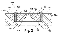
図2〜6は、チップ102および例えば、キャリア・プレート又はマイクロタイター・プレートから構成されてよいキャリア構造104を有して成る本発明のチップ・アッセンブリ100の様々な態様を示している。チップ102は、キャリア構造104のアパーチャー110に受容される。チップ102の外壁105とキャリア構造104の内壁107との間のギャップが存在するように、チップ102の直径はアパーチャー110の直径よりもわずかに小さい。チップ102は、チップ102の外壁105とアパーチャー110の内壁107との間の液密封止106でアパーチャー110に設けられる。
2-6 illustrate various aspects of a
図2〜6に示される態様では、孔108は、図1を参照しつつ上記に説明するように、例えばパッチ・クランプ分析のため、チップ102に試験アイテムを固定するためにチップ102に形成される。この態様では、孔108は貫通孔である。
In the embodiment shown in FIGS. 2-6, holes 108 are formed in the
又、本発明の好ましい態様では、シール106はキャリア構造104にチップ102を接合するため接合材を形成する。
Also, in a preferred embodiment of the present invention, the
好ましくは、接合材は、液体状態でチップ102とキャリア構造104との間のギャップに適用され、続いてチップ102とキャリア構造104との間の永久的な接合を形成する固体状又は高粘度状態にまで硬化される。チップ102の外壁105とキャリア構造104の内壁107との間のボンディング材106の供給はチップ・アッセンブリ100の製造の際、間に行うことができ、ボンディング材を1つ又はそれよりも多い供給ウェルからアパーチャーに供給し、毛管作用によりチップ102とキャリア構造104との間のギャップに流し込むことが可能であるということが分かっている。
Preferably, the bonding material is applied to the gap between the
毛管作用によりボンディング材をギャップに均一に供給することを可能とするために、好ましくは、硬化前にキャリア構造104と周囲雰囲気、例えば大気との間の界面の界面エネルギー密度は、キャリア構造104とボンディング材106との間の界面の界面エネルギー密度よりも大きくなるようなボンディング材106が選択される。最も好ましくは、キャリア構造とボンディング材との間の界面の界面エネルギー密度と、チップとボンディング材との間の界面の界面エネルギー密度との合計は、ボンディング材と周囲雰囲気、例えば大気との間の界面の界面エネルギー密度よりも小さい。本明細書で使用する、用語「界面エネルギー密度」は表面張力、すなわち、単位長さ当たりの力と理解されてよい。
Preferably, the interfacial energy density at the interface between the
ボンディング材の粘度は、毛管作用によりボンディング材が流れ、チップ102とキャリア構造104との間のギャップに均一に供給することができることに影響する。本発明の好ましい態様では、ボンディング材は適用温度で、例えば室温で、又は上昇させた供給温度で硬化前に1〜100000mPa・s、例えば5〜50000mPa・s、10〜1000mPa・s、50〜500mPa・sの粘性、より好ましくは150〜400mPa・sの粘性を有している。チップがキャリア構造の上面に設けられる場合では、毛管作用は接着剤の供給に重要な役割を果たさない。それ故、高粘度を概して適用することが可能である。より具体的には、1000〜200000mPa・s、好ましくは50000〜150000mPa・s、例えば約100000mPa・sの粘度が最も有益であると分かっている。
The viscosity of the bonding material affects the ability of the bonding material to flow due to capillary action and be uniformly supplied to the gap between the
更に、適用の間にボンディング材の更なる供給を成し遂げるために、ボンディング材の硬化前に大気圧下、すなわち、1バールの大気中に設けられる際、ボンディング材は好ましくは90°未満のキャリア構造との接触角を形成する。
Furthermore, in order to achieve a further supply of the bonding material during application, atmospheric pressure prior to curing of the bonding material, i.e., 1 bar when provided in the atmosphere, Bo bindings material preferably less than 90 ° Carrier Forms a contact angle with the structure.
例えば、ボンディング材は、ホットメルト接着剤、アクリルUV硬化接着剤、エポキシ系UV硬化接着剤から構成される群から選択されてよい。例えば、下記の接着剤の1つが適用されてよい。
−20〜25℃で約150mPa・sの粘度を有するアクリル系UV硬化接着剤
−20〜25℃で約400mPa・sの粘度を有するエポキシ系UV硬化接着剤
−20〜25℃で約300mPa・sの粘度を有するアクリル系UV硬化接着剤
For example, the bonding material may be selected from the group consisting of a hot melt adhesive, an acrylic UV curable adhesive, and an epoxy UV curable adhesive. For example, one of the following adhesives may be applied.
Acrylic UV curable adhesive having a viscosity of about 150 mPa · s at -20 to 25 ° C An epoxy UV curable adhesive having a viscosity of about 400 mPa · s at -20 to 25 ° C and about 300 mPa · s at -20 to 25 ° C UV curing adhesive having a viscosity of
チップがキャリア構造の上面に設けられる態様では、供給する温度で非液状である接着剤が適用されてよい。1成分又は2成分熱硬化性エポキシ系接着剤又はシアノ−アクリレート接着剤等の熱硬化性エポキシ系接着剤が有益であると分かっている。好ましくは、これらタイプの接着剤は、供給温度で約1000〜200000mPa・s、例えば好ましくは約100000mPa・s又は約50000mPa・s、例えば1〜200000mPa・s、例えば5〜100000mPa・s、例えば10000〜100000mPa・s、例えば35000〜75000mPa・s、例えば40000〜60000mPa・sの粘度を有するために選択される。 In embodiments where the chip is provided on the top surface of the carrier structure, an adhesive that is non-liquid at the supplied temperature may be applied. Thermosetting epoxy adhesives such as one or two component thermosetting epoxy adhesives or cyano-acrylate adhesives have been found to be beneficial. Preferably, these types of adhesives are about 1000 to 200000 mPa · s at the feed temperature, such as preferably about 100000 mPa · s or about 50000 mPa · s, such as 1 to 200000 mPa · s, such as 5 to 100000 mPa · s, eg 10000 Selected to have a viscosity of 100000 mPa · s, for example 35000-75000 mPa · s, for example 40000-60000 mPa · s.
セル等の生体物質のマイクロ流体分析間の生体適合性を確保するために、生体適合性のあるボンディング材が使用されてよい。湿気および/又は加熱がボンディングを高めるために適用されてよい。 In order to ensure biocompatibility during microfluidic analysis of biological materials such as cells, biocompatible bonding materials may be used. Moisture and / or heating may be applied to enhance bonding.
図2および3の態様では、キャリア構造104のアパーチャー110は、チップの厚さと本質的に(又は実質的に又はほとんど;essentially)同じであるアパーチャーの深さにカラー112を形成する。カラー112上にはチップ102の下面113の縁がある。チップ102の上面115は、望ましくない方法で(図1に示す)マイクロ流体フロー・ドメイン122の分析流体を集めるかもしれない、又は望ましくないフロー渦を形成するかもしれないエッジ又は窪みを避けるためにキャリア構造104の上面101と面一状である。図2の態様では、ボンディング材106は、キャリア構造104の上面101のレベル(又は高さ;level)よりも下方にあるチップ102とキャリア構造104との間のギャップに完全に含まれ、図3の態様では、キャリア構造の上面101の高さよりも上方に突き出るように、少し過剰のボンディング材106が供される。そのような突起は、マイクロ流体フロー・ドメイン122での分析流体の流れを干渉しない程度に、又流体を集めない程度の条件を満たしていてよい。図2〜3の態様でのカラー112の突起により、チップ102の下面113はキャリア構造104の下面109よりも上昇レベルにある。カラー112により、キャリア構造104に対してチップ102を正確に設けることが可能である。
In the embodiment of FIGS. 2 and 3, the
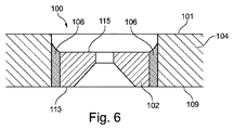
図4は、キャリア構造204の態様を有して成るチップ・アッセンブリ100を示している。チップが、キャリア構造204の傾斜した上面206により形成されたウェルの底部にあるアパーチャー210に設けられている。チップ102の下面113は、図11〜13を参照して下記に説明するように、チップおよびキャリア構造を本発明の第2態様の方法の態様により組み立てることができるためにキャリア構造204の下面205と面一状にある。図6の態様では、キャリア構造104の厚さはチップ102の厚さを上回り、それによって、チップ102の上面115はキャリア構造104の上面101よりも低い高さとなる。
FIG. 4 shows a
図5は本発明の第3態様を示す。キャリア構造104の上面101の略上にある下面113を有するチップ102が、チップ102の下方の縁に沿ってシールするボンディング材106で設けられる。チップ102中の貫通孔108が、図1に概して示すように孔108に設けられたセル等の試験アイテムのマイクロ流体分析、例えばパッチ・クランプ分析のためのキャリア104中のアパーチャー110と本質的に同軸上に設けられる。
FIG. 5 shows a third embodiment of the present invention. A
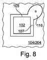
ボンディング材106を、図2〜4および6の態様でのチップ102とキャリア構造104、204との間のギャップに均一に分配することを可能とするために、図7〜9に示す1つ又はそれよりも多い供給ウェル114、116、118を有したキャリア構造104、204が供されてよい。ボンディング材を適用するためシリンジ等の外部デバイスが、供給ウェル114、116、118中に又は上に設けられてよく、それによって、液体ボンディング材が毛管作用によりチップ102とキャリア構造104、204との間のギャップに流れ込み、ギャップを塞いでよい。図7の態様では、単一の供給ウェル114はキャリア構造中のアパーチャー110の一端に供され、図8の態様では、単一の供給ウェル116がアパーチャー110の1つの角に供される。図9に示すように、複数の供給ウェル118がアパーチャー110の各端部に供されてよい。最終製品では、ボンディング材106が硬化した際、チップ102とキャリア構造104、204との間のギャップは、ボンディング材で満たされているキャリア中の少なくとも1つの供給ウェル114、116、118と連通する。
In order to allow the
本発明の他の態様では、チップ102は、キャリア構造104内にプレス・フィットされてよい(又はキャリア構造104内に押し込まれてよい)。例えば、ボンディング材は、チップ102がキャリア構造中のアパーチャー110、210に設けられる前に、キャリア構造104、204の内壁107に沿って適用される成形材から形成されてよい。続いて、チップ102は、ボンディング材を形成する成形材により形成されるパッキング内にプレス・フィット(又は圧入;pressfit)されてよい。
In other aspects of the invention, the
本発明のチップ・アッセンブリは、図10に示されるようにキャリア構造104、204中の各アパーチャーに受容されるチップのアレイとして供されてよい。例えば、全部で128以上のチップ102が単一のキャリア構造に供されてよい。
The chip assembly of the present invention may be provided as an array of chips received in each aperture in the
マイクロ流体分析を行う目的のため、チップ102およびキャリア104、204が、チップにより支持される試験アイテムを介して、例えばセル120を介して(図1に示す)第1ドメイン122と第2ドメイン(図示していない)とに分離するために設けられてよい。キャリア構造104は、有利には一方の電極によるイオンの運搬および他方の電極によるイオンの受取による電極間に電流を生じさせることが可能な複数の電極を支持してよい。例えば、チップ102は、イオン・チャネル含有構造を保持し、イオン・チャネル含有構造の第1の側に規定される第1ドメインとイオン・チャネル含有構造の第2の側に規定される第2ドメインとを分離するために設けられてよい。キャリアは、第1ドメイン122と電気的に接触する第1の電極を支持し、第2ドメインと電気的に接触する第2の電極を支持するために設けられてよい。
For the purpose of performing microfluidic analysis, the
図10の態様では、好ましくは、各電極はチップの各々と関連していることで、各チップは個々の測定部位を供する。 In the embodiment of FIG. 10, preferably each electrode is associated with each of the tips so that each tip provides an individual measurement site.
本発明の態様は、高い処理能力および信頼性で、又、セル又はセル膜が影響を受ける実際の条件下で、セル膜等のイオン・チャネル含有構造を介した電流フローを測定し又は監視するために有益であるかもしれない。従って、測定される結果、例えば、様々な試験化合物等でセル膜に影響を与える結果としてのイオン・チャネル活性の変化は、測定システムにより導かれるアーチファクトではない影響特性の真の兆候として信頼され得、又、所定の条件でのセル膜の伝導性又はキャパシタンスに関連する電気生理学的現象を研究するための有効な根拠として使用され得る。 Aspects of the present invention measure or monitor current flow through ion channel containing structures, such as cell membranes, with high throughput and reliability, and under actual conditions where the cell or cell membrane is affected. May be beneficial for. Thus, changes in ion channel activity that are measured, for example, as a result of affecting the cell membrane with various test compounds, etc., can be trusted as a true sign of an influence characteristic that is not an artifact introduced by the measurement system. It can also be used as an effective basis for studying electrophysiological phenomena related to the conductivity or capacitance of cell membranes under certain conditions.
何故なら、1つ又はそれよりも多いイオン・チャネルを通る電流は、可逆の電極、典型的には下記に特徴づけられるような測定電極および参照電極としての銀/塩化銀等のハロゲン化銀電極を使用して直接的に測定されるからである。 Because the current through one or more ion channels is a reversible electrode, typically a silver halide electrode such as silver / silver chloride as a measurement and reference electrode as characterized below It is because it is measured directly using.
本発明の態様は、セル膜だけではなく、人工膜等の他のイオン・チャネル含有構造での測定のために使用されてよい。本発明では、同時に、独立してイオン移送チャネルおよび膜での電気生理学的測定等のいくつかの試験を行うことが可能である。本発明の基質は、
ごく少量の支持液体(生理食塩水、通常150ミリモルの浸透圧のNaCl又は別の適当な塩を有するセルを有する等張液)および少量の試験サンプルを使用する完全で容易に操作されるマイクロシステムを構成する。
Aspects of the present invention may be used for measurements on other ion channel containing structures such as artificial membranes as well as cell membranes. In the present invention, it is possible to simultaneously perform several tests such as electrophysiological measurements on the ion transport channel and the membrane independently. The substrate of the present invention comprises
Complete and easy-to-operate microsystem using a very small amount of support liquid (saline, usually 150 mM osmotic NaCl or an isotonic solution with a cell with another suitable salt) and a small amount of test sample Configure.
一般的に、本発明の態様は、参照により本明細書に組み入れられているWO01/25769およびWO03/089564に開示されている使用分野でとりわけ適用することが可能である。 In general, the embodiments of the present invention are particularly applicable in the fields of use disclosed in WO01 / 25769 and WO03 / 089564, which are incorporated herein by reference.
図7の寸法e、fであるチップ102の直径は0.1〜2mm、例えば0.5〜1.5mm、例えば約1mmであってよい。チップ102が四角形の態様では、e、fの寸法は同一である。しかしながら、チップ102が長方形の態様では、これら寸法は異なる。図7の寸法c、dであるキャリア構造104、204中のアパーチャー110、210の寸法は、好ましくは約1mmの直径であるチップ102の直径よりも約10〜30%大きく、例えば約0.2〜2.5mm、例えば0.8〜1.5mm、例えば約1.2mmである。そのような態様では、全容積が約1〜2μlであるボンディング材が、キャリア構造に取り付け、密封するために適用される。
7 may have a diameter of 0.1 to 2 mm, for example 0.5 to 1.5 mm, for example about 1 mm. When the
キャリア構造104、204およびチップ102は、図2〜4、6および11〜13で異なる厚さで示されているが、略同じ厚さを有していてよい。厚さは好ましくは2mm未満、例えば0.3〜0.6mm、例えば約0.5mmである。
The
好ましくは、チップの投影面積、すなわちチップの上面および下面の表面積は、チップが精密な条件により製造可能なシリコン又は他の高価な材料の使用を最小限にするために最大5mm2、例えば最大3mm2、2mm2、1.5mm2又は1mm2である。 Preferably, the projected area of the chip, ie the surface area of the top and bottom surfaces of the chip, is a maximum of 5 mm 2 , for example a maximum of 3 mm, in order to minimize the use of silicon or other expensive materials that the chip can be manufactured with precise conditions 2 , 2 mm 2 , 1.5 mm 2 or 1 mm 2 .
チップは、ウェーハ切断技術により又はステルス・ダイシング等のダイシングにより所望の寸法に切断されてよい。チップは、参照により本明細書に組み入れられている、例えばWO03/089564に開示された原理および例に従って製造されてよい。好ましくは、チップは、小さな寸法のチップ、すなわち、最大で5mm2の投影面積を有するチップに特に適した方法を構成すると分かっているレーザー切断によりSiウェーハから切断される。 The chips may be cut to the desired dimensions by wafer cutting techniques or by dicing such as stealth dicing. The chip may be manufactured according to the principles and examples disclosed, for example, in WO 03/089564, which is incorporated herein by reference. Preferably, the chips are cut from the Si wafer by laser cutting which has been found to constitute a particularly suitable method for small sized chips, ie chips having a projected area of at most 5 mm 2 .
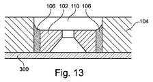
図11〜13は、チップ102はアパーチャー中に設けられ、液密封止がチップの外壁とアパーチャーの内壁との間に形成される本発明の第2態様に従った方法の態様を示している。
FIGS. 11-13 show an embodiment of the method according to the second aspect of the invention in which the
一般的に、図11〜13に示される方法は、
−ボンディング材で前記ギャップを塞ぐ前にキャリア構造の一方の側にテープを貼り付ける工程、および
−ボンディング材でギャップを塞いだ後、テープを取り除く工程を含んで成る。チップは、ギャップがボンディング材で塞がれる前にアパーチャーに設けられる。チップは、タップがキャリア構造に取り付けられる前に、又はその後に設けられてよい。
In general, the method shown in FIGS.
A step of applying a tape to one side of the carrier structure before closing the gap with the bonding material, and a step of removing the tape after closing the gap with the bonding material. The chip is provided in the aperture before the gap is closed with the bonding material. The tip may be provided before or after the tap is attached to the carrier structure.
図11はアパーチャー110を有するキャリア構造104を示す。テープ、好ましくは接着テープ300は、上方に面する、すなわちアパーチャー110に対して接着側面を有するキャリア構造104の一方の側に取り付けられる。続いて、図12に示すように、チップ102は、チップの外壁とキャリア構造の内壁との間にギャップを有したアパーチャーに設けられる。それ故、チップ102の下面がテープ300の接着側面に位置し、それによって、ボンディング材106が適用されるまで、テープがキャリア構造104にチップ102を間欠的に固定する。続いて、図13に示すように、ボンディング材106が、図7〜9を参照して上記にて説明するようにギャップに充填され、分配される。続いて、ボンディング材106が硬化され、最終的にテープ300が最終製品に到達するために除去される。好ましい態様では、接着剤は、ボンディング材の硬化の間その粘着性を失う。例えば、テープの粘着性はUV光にさらされる際に接着性能を失うかもしれず、それによって、UV照射によりボンディング材を硬化する際に、テープがキャリア構造から引き離される。
FIG. 11 shows a
Claims (5)
−外壁および下面を有し、外面を規定するチップ、
−上面を有し、および内壁を規定するアパーチャーを有して成る、キャリア構造
を有して成り、
前記チップが、該チップと前記キャリア構造との間にリキッドタイト・シールを形成するボンディングおよびシーリング材により前記キャリア構造の上部にて前記キャリア構造に固定されており、
前記チップは、該チップの前記下面が前記キャリア構造の略前記上面上にあるように設けられており、
前記ボンディングおよび前記シーリング材は、前記チップの前記外面の付近の前記外壁および前記下面に沿い、前記チップの前記外面に沿って供され、および、
前記キャリア構造中の前記アパーチャーと本質的に同軸上に設けられている孔が、前記チップに形成されている、チップ・アッセンブリ。 A chip assembly for use in a microfluidic analysis system for measuring and / or monitoring the electrophysiological properties of an ion channel in an ion channel-containing structure comprising :
- it possesses an outer wall and a lower surface, defining an outer surface chip,
-Having a carrier structure comprising an upper surface and having an aperture defining an inner wall;
The chip is secured to the carrier structure at the top of the carrier structure by a bonding and sealing material that forms a liquid tight seal between the chip and the carrier structure ;
The chip is provided such that the lower surface of the chip is substantially above the upper surface of the carrier structure;
The bonding and sealing material are provided along the outer wall and the lower surface in the vicinity of the outer surface of the chip, along the outer surface of the chip; and
It said aperture essentially holes provided coaxially in the carrier structure is formed on the chip, the chip assembly.
−外壁および下面を有し、外面を規定するチップであって、該チップに孔が供されているチップ、
−上面を有し、および内壁を規定するアパーチャーを有して成る、キャリア構造、
−前記チップと前記キャリア構造との間にリキッドタイト・シールを形成するためのボンディングおよびシーリング材を有して成り、
該方法が、
−前記ボンディングおよび前記シーリング材により、前記キャリア構造中の前記アパーチャーと本質的に同軸上に設けられた前記孔を有し、および前記下面が前記キャリア構造の略前記上面上にあるように設けた前記チップを、前記キャリア構造の上部にて前記キャリア構造に固定する工程を含んで成り、
前記固定工程では、前記チップと前記キャリア構造との間に前記リキッドタイト・シールを形成するために、前記ボンディングおよび前記シーリング材を前記チップの前記外面の付近の前記外壁および前記下面に沿い前記チップの前記外面に沿って供する、方法。 A method of manufacturing a chip assembly for use in a microfluidic analysis system for measuring and / or monitoring electrophysiological properties of an ion channel in an ion channel-containing structure comprising :
- possess an outer wall and a lower surface, a tip defining an outer surface, a chip hole in the chip has been put,
- has a top surface, and comprising a aperture defining an inner wall, the carrier structure,
-Comprising a bonding and sealing material for forming a liquid tight seal between the chip and the carrier structure ;
The method is
- by the bonding and the sealing member has the apertures essentially the holes provided coaxially in the carrier structure, and the lower surface is provided to be on substantially the upper surface of the carrier structure the chip, comprises a more engineering to be fixed to the carrier structure at the top of the carrier structure,
In the fixing step, in order to form the liquid tight seal between the chip and the carrier structure, the bonding and the sealing material are disposed along the outer wall and the lower surface in the vicinity of the outer surface of the chip. A method of providing along the outer surface .
Applications Claiming Priority (5)
| Application Number | Priority Date | Filing Date | Title |
|---|---|---|---|
| US36292610P | 2010-07-09 | 2010-07-09 | |
| US61/362,926 | 2010-07-09 | ||
| EP11157598 | 2011-03-10 | ||
| EP11157598.1 | 2011-03-10 | ||
| PCT/EP2011/061390 WO2012004297A1 (en) | 2010-07-09 | 2011-07-06 | A chip assembly for use in a microfluidic analysis system |
Publications (3)
| Publication Number | Publication Date |
|---|---|
| JP2013536407A JP2013536407A (en) | 2013-09-19 |
| JP2013536407A5 JP2013536407A5 (en) | 2014-08-21 |
| JP5851500B2 true JP5851500B2 (en) | 2016-02-03 |
Family
ID=43983374
Family Applications (1)
| Application Number | Title | Priority Date | Filing Date |
|---|---|---|---|
| JP2013517374A Active JP5851500B2 (en) | 2010-07-09 | 2011-07-06 | Chip assembly for use in microfluidic analysis systems |
Country Status (7)
| Country | Link |
|---|---|
| US (2) | US20130136673A1 (en) |
| EP (1) | EP2590743B1 (en) |
| JP (1) | JP5851500B2 (en) |
| CN (1) | CN103068486B (en) |
| CA (1) | CA2804564A1 (en) |
| DK (1) | DK2590743T3 (en) |
| WO (2) | WO2012004296A1 (en) |
Families Citing this family (10)
| Publication number | Priority date | Publication date | Assignee | Title |
|---|---|---|---|---|
| EP2681550B1 (en) | 2011-03-01 | 2016-07-06 | Sophion Bioscience A/S | Handheld device for electrophysiological analysis |
| CA2860501C (en) | 2012-01-09 | 2021-05-18 | Sophion Bioscience A/S | Improved patch area cell adhesion |
| DE102012112306A1 (en) | 2012-12-14 | 2014-06-18 | Thinxxs Microtechnology Ag | Method for connecting components of a microfluidic flow cell |
| CN104122226B (en) * | 2013-04-25 | 2016-06-01 | 黄辉 | The method for packing of a kind of optics micro-fluidic biological sensor |
| KR102447394B1 (en) | 2015-12-03 | 2022-09-27 | 프리시젼바이오 주식회사 | Fluid analysis cartridge and fluid analysis apparatus having the same |
| CN106391151B (en) * | 2016-08-31 | 2018-11-09 | 清华大学 | It is suitable for the multilayer micro-fluid chip production method of mass production |
| CN107199060B (en) * | 2017-05-17 | 2019-07-26 | 清华大学深圳研究生院 | A kind of three-dimensional electrofocusing's micro-fluidic chip and preparation method thereof for solid phase microextraction |
| CN109097264B (en) * | 2018-07-31 | 2021-10-15 | 大连理工大学 | Microfluidic cell adsorption chip for cell patch clamp |
| CN109647557B (en) * | 2019-02-27 | 2021-04-02 | 哈尔滨工业大学 | Direct particle separation chip based on induced charge electroosmosis micro vortex and application and separation method thereof |
| CN110482483B (en) * | 2019-08-07 | 2022-05-20 | 北京自动化控制设备研究所 | Sensitive structure patch system and method for MEMS device |
Family Cites Families (21)
| Publication number | Priority date | Publication date | Assignee | Title |
|---|---|---|---|---|
| IL68507A (en) * | 1982-05-10 | 1986-01-31 | Univ Bar Ilan | System and methods for cell selection |
| JP3486171B2 (en) | 1997-12-17 | 2004-01-13 | エコル・ポリテクニック・フェデラル・ドゥ・ロザンヌ(エ・ペー・エフ・エル) | Positioning and electrophysiological characterization of single cell and reconstituted membrane systems on microstructured carriers |
| CN1204404C (en) * | 1999-10-01 | 2005-06-01 | 索菲昂生物科学有限公司 | Substrate and method for determining and/or monitoring electrophysiological properties of ion channels |
| US7175980B2 (en) * | 2000-10-30 | 2007-02-13 | Sru Biosystems, Inc. | Method of making a plastic colorimetric resonant biosensor device with liquid handling capabilities |
| CN1369709A (en) * | 2001-02-12 | 2002-09-18 | 阎小君 | Combined biochip and its preparing process |
| US20050212095A1 (en) | 2002-04-17 | 2005-09-29 | Sophion Bioscience A/S | Substrate and method for measuring the electrophysiological properties of cell membranes |
| GB2398635A (en) | 2003-02-21 | 2004-08-25 | Sophion Bioscience As | A substrate providing a cell gigaseal for a patch clamp |
| EP1501924A4 (en) * | 2002-05-04 | 2006-05-24 | Aviva Biosciences Corp | Apparatus including ion transport detecting structures and methods of use |
| JP4552423B2 (en) * | 2003-11-21 | 2010-09-29 | パナソニック株式会社 | Extracellular potential measuring device and method for measuring extracellular potential using the same |
| DE10345817A1 (en) * | 2003-09-30 | 2005-05-25 | Boehringer Ingelheim Microparts Gmbh | Method and apparatus for coupling hollow fibers to a microfluidic network |
| CN100536097C (en) * | 2005-07-25 | 2009-09-02 | 皇家飞利浦电子股份有限公司 | Interconnection and packaging method for biomedical devices with electronic and fluid functions |
| JP4661539B2 (en) * | 2005-11-11 | 2011-03-30 | パナソニック株式会社 | Cell electrophysiological sensor and manufacturing method thereof |
| KR100705642B1 (en) * | 2005-12-29 | 2007-04-09 | 삼성전자주식회사 | Nozzle for inkjet printer head and method of manufacturing thereof |
| WO2008086893A1 (en) * | 2007-01-17 | 2008-07-24 | Agilent Technologies, Inc. | Microfluidic chip with lateral opening for fluid introduction |
| CN201066356Y (en) * | 2007-07-06 | 2008-05-28 | 徐涵 | Biological chip based on plant mixing micro-array |
| CN201066365Y (en) | 2007-08-14 | 2008-05-28 | 周兆强 | A connection box of power measuring device |
| WO2009081521A1 (en) * | 2007-12-20 | 2009-07-02 | Panasonic Corporation | Process for producing cell electrophysiological sensor and apparatus for producing the cell electrophysiological sensor |
| JP4973618B2 (en) * | 2007-12-20 | 2012-07-11 | パナソニック株式会社 | Cell electrophysiological sensor manufacturing method and manufacturing apparatus |
| CN102026724B (en) * | 2008-05-13 | 2014-03-12 | Nxp股份有限公司 | Sensor array and method of manufacturing same |
| JP2010043928A (en) * | 2008-08-12 | 2010-02-25 | Seiko Epson Corp | Manufacturing method of biochip, and the biochip |
| JP2010101819A (en) * | 2008-10-27 | 2010-05-06 | Panasonic Corp | Cell electrophysiological sensor |
-
2011
- 2011-07-06 CA CA2804564A patent/CA2804564A1/en not_active Abandoned
- 2011-07-06 DK DK11731321.3T patent/DK2590743T3/en active
- 2011-07-06 WO PCT/EP2011/061388 patent/WO2012004296A1/en active Application Filing
- 2011-07-06 US US13/809,097 patent/US20130136673A1/en not_active Abandoned
- 2011-07-06 CN CN201180040062.XA patent/CN103068486B/en not_active Expired - Fee Related
- 2011-07-06 JP JP2013517374A patent/JP5851500B2/en active Active
- 2011-07-06 WO PCT/EP2011/061390 patent/WO2012004297A1/en active Application Filing
- 2011-07-06 EP EP11731321.3A patent/EP2590743B1/en active Active
-
2016
- 2016-07-25 US US15/218,642 patent/US9975120B2/en active Active
Also Published As
| Publication number | Publication date |
|---|---|
| EP2590743A1 (en) | 2013-05-15 |
| JP2013536407A (en) | 2013-09-19 |
| CA2804564A1 (en) | 2012-01-12 |
| US20130136673A1 (en) | 2013-05-30 |
| EP2590743B1 (en) | 2016-06-29 |
| CN103068486A (en) | 2013-04-24 |
| US20160332160A1 (en) | 2016-11-17 |
| WO2012004297A1 (en) | 2012-01-12 |
| DK2590743T3 (en) | 2016-09-12 |
| WO2012004296A1 (en) | 2012-01-12 |
| CN103068486B (en) | 2015-09-23 |
| US9975120B2 (en) | 2018-05-22 |
Similar Documents
| Publication | Publication Date | Title |
|---|---|---|
| JP5851500B2 (en) | Chip assembly for use in microfluidic analysis systems | |
| US8354271B2 (en) | Biosensor | |
| JP6782296B2 (en) | Plasma separation microfluidic device | |
| AU2017237981A1 (en) | Wafer-scale assembly of insulator-membrane-insulator devices for nanopore sensing | |
| DK2394156T3 (en) | Device and method for electrochemical measurement of biochemical reactions as well as method of preparation for the device. | |
| CN101501485B (en) | Method for analysis of sample by capillary electrophoresis | |
| US20090194429A1 (en) | Apparatus and Method for Sensing a Time Varying Ionic Current in an Electrolytic System | |
| US7608417B2 (en) | Cell electro-physiological sensor and method of manufacturing the same | |
| CN101663578B (en) | Electrophoresis chip and electrophoresis apparatus | |
| US20080206828A1 (en) | Device For Introducing Substance Into Cell, Cell Clamping Device and Flow Path Forming Method | |
| US20100203621A1 (en) | Biosensor | |
| Tang et al. | Lateral patch-clamping in a standard 1536-well microplate format | |
| JP2007174990A (en) | Cellular electrophysiological sensor array and method for producing the same | |
| JP2008039624A (en) | Cell electrophysiologic sensor and its manufacturing method | |
| JP2008000079A (en) | Physiological sensor for cellular electricity | |
| JP4670713B2 (en) | Cell electrophysiological sensor and cell electrophysiological measurement method using the same | |
| JP4597710B2 (en) | Micro mass detection chip | |
| Zhang et al. | Recent advances of nanopore technique in single cell analysis | |
| CA2573025A1 (en) | High density ion transport measurement biochip devices and methods | |
| JP2007218716A (en) | Cell electrophysiological sensor | |
| WO2012077325A1 (en) | Silicon structure, array substrate using same, and method for producing silicon structure | |
| JP2011205995A (en) | Electrophysiological measurement device | |
| JP2007278960A (en) | Cell electric physiological sensor, and method of measuring cell electric physiological phenomenon using this | |
| JP2021120620A (en) | Fluid for particle detection | |
| JP2007333570A (en) | Cell electrophysiological sensor and method for measuring cell electrophysiological phenomenon using same |
Legal Events
| Date | Code | Title | Description |
|---|---|---|---|
| A521 | Request for written amendment filed |
Free format text: JAPANESE INTERMEDIATE CODE: A523 Effective date: 20140704 |
|
| A621 | Written request for application examination |
Free format text: JAPANESE INTERMEDIATE CODE: A621 Effective date: 20140704 |
|
| A977 | Report on retrieval |
Free format text: JAPANESE INTERMEDIATE CODE: A971007 Effective date: 20150320 |
|
| A131 | Notification of reasons for refusal |
Free format text: JAPANESE INTERMEDIATE CODE: A131 Effective date: 20150407 |
|
| A601 | Written request for extension of time |
Free format text: JAPANESE INTERMEDIATE CODE: A601 Effective date: 20150702 |
|
| A521 | Request for written amendment filed |
Free format text: JAPANESE INTERMEDIATE CODE: A523 Effective date: 20151006 |
|
| TRDD | Decision of grant or rejection written | ||
| A01 | Written decision to grant a patent or to grant a registration (utility model) |
Free format text: JAPANESE INTERMEDIATE CODE: A01 Effective date: 20151110 |
|
| A61 | First payment of annual fees (during grant procedure) |
Free format text: JAPANESE INTERMEDIATE CODE: A61 Effective date: 20151202 |
|
| R150 | Certificate of patent or registration of utility model |
Ref document number: 5851500 Country of ref document: JP Free format text: JAPANESE INTERMEDIATE CODE: R150 |
|
| R250 | Receipt of annual fees |
Free format text: JAPANESE INTERMEDIATE CODE: R250 |
|
| R250 | Receipt of annual fees |
Free format text: JAPANESE INTERMEDIATE CODE: R250 |
|
| R250 | Receipt of annual fees |
Free format text: JAPANESE INTERMEDIATE CODE: R250 |
|
| R250 | Receipt of annual fees |
Free format text: JAPANESE INTERMEDIATE CODE: R250 |
|
| R250 | Receipt of annual fees |
Free format text: JAPANESE INTERMEDIATE CODE: R250 |
|
| R250 | Receipt of annual fees |
Free format text: JAPANESE INTERMEDIATE CODE: R250 |