JP2010101819A - Cell electrophysiological sensor - Google Patents
Cell electrophysiological sensor Download PDFInfo
- Publication number
- JP2010101819A JP2010101819A JP2008275113A JP2008275113A JP2010101819A JP 2010101819 A JP2010101819 A JP 2010101819A JP 2008275113 A JP2008275113 A JP 2008275113A JP 2008275113 A JP2008275113 A JP 2008275113A JP 2010101819 A JP2010101819 A JP 2010101819A
- Authority
- JP
- Japan
- Prior art keywords
- hole
- sensor chip
- protrusions
- present
- protrusion
- Prior art date
- Legal status (The legal status is an assumption and is not a legal conclusion. Google has not performed a legal analysis and makes no representation as to the accuracy of the status listed.)
- Pending
Links
Images


Abstract
Description
本発明は、創薬スクリーニング等に利用できる細胞電気生理センサに関する。 The present invention relates to a cell electrophysiological sensor that can be used for drug discovery screening and the like.
電気生理学におけるパッチクランプ法は、細胞膜に存在するイオンチャンネルを測定する方法として知られており、この自動化システムとして、細胞電気生理ンセンサがある。 The patch clamp method in electrophysiology is known as a method of measuring ion channels existing in a cell membrane, and a cell electrophysiology sensor is known as this automated system.
図8に示す従来の細胞電気生理センサは、貫通孔1を有する実装部2と、貫通孔1に挿入されたセンサチップ3を備え、このセンサチップ3は、導通孔4が設けられた薄板5を有している。また貫通孔1の内壁には、センサチップ3の上端に接する突起部6が形成され、この突起部6によりセンサチップ3の位置決めが高精度になる。
The conventional cell electrophysiological sensor shown in FIG. 8 includes a
ここでこのセンサチップ3の上方および下方を電解液で満たし、さらに細胞を上方から注入し、吸引等すると、導通孔4の開口部に細胞を密着保持することができる。そしてこの状態で、細胞の上から薬剤を投与し、その後細胞の上下の電位差を電極で測定すれば、細胞の薬理反応を分析することができる。 Here, when the upper and lower portions of the sensor chip 3 are filled with the electrolytic solution, and the cells are injected from above and sucked, the cells can be held in close contact with the opening of the conduction hole 4. In this state, if a drug is administered from above the cell and then the potential difference between the upper and lower cells is measured with an electrode, the pharmacological reaction of the cell can be analyzed.
なお、上記従来技術に関連する技術は、下記特許文献に開示されている。
従来の細胞電気生理センサでは、薄板5の表面を気泡が覆ってしまい、測定が出来なくなることがあった。 In the conventional cell electrophysiological sensor, the surface of the thin plate 5 may be covered with bubbles, and measurement may not be possible.
その理由は、突起部6が、貫通孔1の内周一帯に沿って形成された環状構造だからである。したがって、この突起部6が形成された領域では、貫通孔1の断面積が小さくなり、気泡が抜け難くなる。そしてその結果、薄板5の表面を気泡が覆ってしまうのである。
The reason is that the
そこで本発明は、薄板5の表面を気泡が覆うのを抑制し、測定精度を向上させることを目的とする。 Therefore, an object of the present invention is to suppress the bubble from covering the surface of the thin plate 5 and improve the measurement accuracy.
そしてこの目的を達成するため本発明は、貫通孔の内壁には、センサチップの端部に接する複数の突起部が形成され、これらの突起部は、それぞれの先端と、隣接する突起部の先端との間に隙間が空くように配置されたものとした。 In order to achieve this object, according to the present invention, the inner wall of the through hole is formed with a plurality of protrusions that are in contact with the ends of the sensor chip, and these protrusions are connected to the respective tips and the tips of the adjacent protrusions. It was assumed that there was a gap between them.
これにより本発明は、薄板の表面を気泡が覆うのを抑制し、測定精度を向上させることができる。 Thereby, this invention can suppress that a bubble covers the surface of a thin plate, and can improve a measurement precision.
その理由は、上述のように、突起部を複数個に分割して配置し、それぞれの先端間に隙間を設けたからである。したがって、隙間の分だけ貫通孔の断面積を大きくすることができる。 The reason is that, as described above, the protrusions are divided into a plurality of parts and a gap is provided between the respective tips. Therefore, the cross-sectional area of the through hole can be increased by the gap.
そしてその結果、薄板の表面を気泡が覆うのを抑制し、測定精度を向上させることができる。 And as a result, it can suppress that a bubble covers the surface of a thin plate, and can improve a measurement precision.
(実施の形態1)
はじめに、本実施の形態における細胞電気生理センサの構造を説明する。
(Embodiment 1)
First, the structure of the cell electrophysiological sensor in the present embodiment will be described.
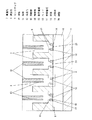
図1に示すように、本実施の形態における細胞電気生理センサは、アレイ状に形成された貫通孔7を有する実装板8と、貫通孔7の内部にそれぞれ挿入され、固定されたセンサチップ9とを備えている。このセンサチップ9は、図1、図2に示すように、貫通孔7の上方と下方とを仕切る円板状の薄板10と、この薄板10の外周を支持する円筒状の枠体11とを有し、薄板10には、その上下面を貫通する導通孔12が形成されている。
As shown in FIG. 1, the cell electrophysiological sensor according to the present embodiment includes a mounting plate 8 having through
なお本実施の形態では、薄板10は、厚み10μm〜100μm、直径1000μm、枠体11は、高さ400μm程度、外径は1000μm、導通孔12は開口径1μm〜3μmφ(深さは薄板10の厚みと同じ)とした。この導通孔12の開口径は5μm以下が細胞を保持するために適している。
In this embodiment, the
また図1に示すように、貫通孔7の内壁には、センサチップ9の上端部、すなわち枠体11の上面に接する二つの突起部13が形成されている。これらの突起部13は、図3、図4に示すように、貫通孔7の水平断面の直径上に、対向して配置され、隣接する突起部13間で隙間が空くように配置されている。特に本実施の形態では、突起部13の先端が細くなっているので、それぞれの突起部13の先端間は、隙間がより大きくなっている。また突起部13は、射出成形が容易になるように、先端が丸みを帯びた形状に形成されている。なお本実施の形態では、図1に示すように、センサチップ9の下端部外縁に接着剤14を塗布し、実装板8に固定している。
As shown in FIG. 1, two
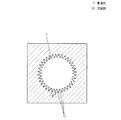
ここでこの貫通孔7の内部空間には、電解液や薬剤等が注入される。本実施の形態では、図3に示すように、貫通孔7の貫通方向に対して垂直な断面は、突起部13よりも上側が四角形であり、容積をより大きくすることができ、気泡の発生を抑制するとともに、電解液等を多く充填することができる。また実装板8の上面における貫通孔7の開口部を四角形とすることにより、アレイ状に配置した場合にも、貫通孔7を連続して多数個配置できる。またプローブ形の電極等を挿入しやすくなる。
Here, an electrolytic solution, a drug, or the like is injected into the internal space of the through
さらに本実施の形態では、貫通孔7の、突起部13よりも下側は、断面が円形となっている。これにより薄板10に平行な断面が円形のセンサチップ9を密着して保持できるとともに、センサチップ9への応力負荷を均等に分散することができ、微細で劈開しやすいセンサチップ9の損傷を抑制できる。なお本実施の形態では、貫通孔7の上方の容積を大きくするため、突起部13の上側の断面積は、下側の断面積よりも大きくしている。
Further, in the present embodiment, the cross section of the through
また本実施の形態では、図1に示すように、貫通孔7内に、上方からプローブ形の測定電極15と細い管状のヘッド16とが挿入されている。
In the present embodiment, as shown in FIG. 1, a probe-shaped measuring
測定電極15は、センサチップ9上方に注入される電解液の電位、あるいは電流値や抵抗値を測定するものである。またヘッド16は、センサチップ9上方に測定液(電解液)や細胞、薬剤等を注入するためのものである。
The
また本実施の形態では、実装板8の下面に参照電極17を設けている。
In the present embodiment, the
さらに実装板8の下方には、流路18が形成された流路板19が接合され、この流路18内には電解液が充填できる。前述の参照電極17は、この電解液の電位(あるいは電流値や抵抗値)を測定できればよく、位置や形状は適宜変更可能である。例えばプローブ形の形状とし、センサチップ9の下方の空間に挿入されていてもよい。
Further, a
次に本実施の形態における部材の説明をする。 Next, members in the present embodiment will be described.
センサチップ9はシリコン単結晶基板、あるいはSOI(Silicon on Insulator)基板、ガラス基板、水晶基板等をエッチングすることにより形成できる。本実施の形態では、センサチップ9として二酸化シリコン層をシリコン層で挟みこんだSOI基板を用い、ドライエッチングにより微細な導通孔12を形成した。なお、SOI基板は、中間の二酸化シリコン層をエッチングストップ層として用いることができる。したがって、導通孔12の深さや薄板10の厚み、枠体11の高さなど、設計通りに高精度に加工することができる。
The
また実装板8、流路板19の材料は、例えば熱可塑性樹脂が挙げられ、ポリカーボネート(PC)、ポリエチレン(PE)、オレフィンポリマー、ポリメタクリル酸メチルアセテート(PMMA)のいずれか、またはこれらの組み合わせが好ましい。
The material of the mounting plate 8 and the
これらの材料からなる実装板8は、紫外線硬化型の接着剤14を用いることによって、容易にセンサチップ9と接合できる。さらに好ましくは、これらの熱可塑性樹脂として、環状オレフィンポリマー、線状オレフィンポリマー、またはこれらが重合した環状オレフィンコポリマー、またはポリエチレン(PE)とすることが作業性、製造コストおよび材料の入手性の観点から好ましい。
The mounting board 8 made of these materials can be easily joined to the
特に、環状オレフィンコポリマーは透明性、アルカリ・酸などの無機系薬剤に対する耐性が強く、本発明の製造方法もしくは使用環境に適している。またこれらの材料は紫外線を透過させることができることから、紫外線硬化型の接着剤14を用いる時に効果を発揮する。
In particular, the cyclic olefin copolymer is highly transparent and highly resistant to inorganic chemicals such as alkalis and acids, and is suitable for the production method or use environment of the present invention. In addition, since these materials can transmit ultraviolet rays, they are effective when the ultraviolet
また本実施の形態では、突起部13は実装板8と一体成形されているため、突起部13の材料は実装板8と同じである。突起部13を、センサチップ9よりも弾性が小さい(軟らかい)材料で構成することによって、センサチップ9の損傷を抑制できる。
In the present embodiment, since the
なお、本実施の形態のように、センサチップ9を実装板8に実装する方法は、実装板8自体に導通孔12を直接形成した場合と比較して、コストも下がり、歩留まりも向上し、さらにリペア性を有する。
Note that, as in the present embodiment, the method of mounting the
次に本実施の形態における細胞電気生理センサを用いた測定方法について説明する。 Next, a measurement method using the cell electrophysiological sensor in the present embodiment will be described.
図1に示すように貫通孔7の上方からヘッド16を挿入し、センサチップ9の上方に細胞外液(電解液)を注入する。
As shown in FIG. 1, the
また流路18の内部には、細胞内液(電解液)を注入する。
In addition, intracellular fluid (electrolytic solution) is injected into the
ここで細胞外液とは例えば哺乳類筋細胞の場合、代表的にはK+イオンが4mM程度、Na+イオンが145mM程度、Cl-イオンが123mM程度添加された電解液であって、細胞内液とは、K+イオンが155mM、Na+イオンが12mM程度、Cl-イオンが4.2mM程度添加された電解液である。 Here, for example, in the case of mammalian muscle cells, the extracellular fluid is typically an electrolytic solution to which about 4 mM of K + ions, about 145 mM of Na + ions, and about 123 mM of Cl − ions are added. Is an electrolyte containing about 155 mM K + ions, about 12 mM Na + ions, and about 4.2 mM Cl − ions.
そして次に、貫通孔7の上方から測定電極15を挿入する。このように細胞外液と電気的に接続された測定電極15と、細胞内液と電気的に接続された参照電極17との間では、100kΩ〜10MΩ程度の導通抵抗値を観測することができる。これは導通孔12を介して細胞内液あるいは細胞外液が浸透し、測定電極15と参照電極17間で電気回路が形成されるからである。
Then, the
次に、センサチップ9上方からヘッド16を介して細胞20を投入する。
Next, the
そして、その後流路18内を減圧すると、図1、図2に示すように細胞20は導通孔12の開口部に引き付けられる。このように細胞20が導通孔12の開口部を塞ぐことによって、細胞外液と細胞内液との間の電気抵抗が1GΩ以上の十分に高い状態となる(ギガシールと呼ぶ)。このギガシール状態では、細胞20の電気生理活動によって細胞内外の電位が変化すれば、わずかな電位差あるいは電流であっても高精度に測定できる。
Then, when the inside of the
次に図1の流路18内の空間にナイスタチンなどの薬剤を注入するか、あるいは針によって導通孔12を塞いでいる細胞膜に穴を開ける(ホールセルと呼ぶ)。
Next, a drug such as nystatin is injected into the space in the
その後センサチップ9上方からヘッド16を介して薬液を注入し、細胞20を刺激する。この時、細胞を刺激する方法としては、本実施の形態のように薬液などの化学的刺激でもよく、その他電気信号などの物理的刺激でも良い。そしてこれらの化学的あるいは物理的刺激によって、細胞のイオンチャネルが反応した場合は、その反応を測定電極15と参照電極17間における電位差(あるいは電流値変化や抵抗値変化)によって検出することができる。
Thereafter, a chemical solution is injected from above the
以下本実施の形態における効果を説明する。 The effects in this embodiment will be described below.
本実施の形態では、前述のように、突起部13を複数個に分割して配置し、それぞれの先端間に隙間を設けたことにより、薄板10の表面を気泡が覆うのを抑制し、測定精度を向上させることができる。
In the present embodiment, as described above, the
すなわち、従来は、図8に示すように、突起部6が、貫通孔1の内周一帯に沿って形成された環状構造であった。したがって、この突起部6が形成された領域では、貫通孔1の断面積が小さくなり、気泡が発生しやすくなっていた。そしてその結果、薄板5の表面を気泡が覆ってしまうのであった。そして例えば薄板5の細胞保持面側を気泡が覆うと、細胞を導通孔4の開口部に密着保持させることができなくなる。また細胞保持面の反対側の面を気泡が覆うと、吸引がしにくくなり、細胞を導通孔4へと引き付けることが出来なくなる。そしていずれの場合も、測定が非常に困難となるのであった。
That is, conventionally, as shown in FIG. 8, the
これに対し本実施の形態では、図3、図4に示すように、突起部13間に隙間を設けたため、この隙間の分だけ貫通孔7の断面積を大きくすることができる。
In contrast, in the present embodiment, as shown in FIGS. 3 and 4, a gap is provided between the
そしてその結果、薄板10の表面を気泡が覆うのを抑制し、測定精度を向上させることができる。
And as a result, it can suppress that a bubble covers the surface of the
なお本実施の形態では、図1の導通孔12に細胞20を引き付ける際、流路18側を減圧している。したがって、気泡が拡張され、薄板10の表面を覆いやすい。したがって、本実施の形態のように、突起部13の形状によって気泡の発生を抑制することは、測定の高精度化に有用である。
In the present embodiment, when the
また本実施の形態では、図3、図4に示すように、突起部13が貫通孔7の断面の直径上に配置されているため、センサチップ9が片寄るのを防止し、安定して保持することができ、位置決めが高精度になる。なお本実施の形態では、突起部13を二つだけ形成したが、図5に示すように、それ以上設けても良く、放射状に配置すれば、安定してセンサチップ9を保持することが出来る。
Further, in the present embodiment, as shown in FIGS. 3 and 4, the
さらに本実施の形態では、突起部13は、先端が細くなる形状であるため、貫通孔7の内部の空間面積をより大きくすることができ、気泡の発生を効率よく抑制することができる。
Further, in the present embodiment, since the
(実施の形態2)
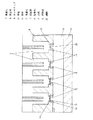
本実施の形態と実施の形態1との違いは、図6に示すように、複数の突起部13が連なるように形成され、それぞれの突起部13の側面と、隣接する突起部13の側面との成す角θが鋭角となるように形成されている点である。これにより本実施の形態では、貫通孔7の内部における気泡の発生を低減し、薄板10表面に気泡が覆うのを抑制し、より高精度に測定することができる。
(Embodiment 2)
As shown in FIG. 6, the difference between the present embodiment and the first embodiment is that a plurality of
その理由を以下に説明する。すなわち従来は、図8に示すように、突起部6の側面上において、貫通孔1の内部に充填される溶液に表面張力が働き、液滴が突起部6の内壁に行き渡りにくくなり、気泡が発生することがあった。
The reason will be described below. That is, conventionally, as shown in FIG. 8, on the side surface of the
これに対し本実施の形態では、隣接する突起部13の側面同士の成す角θは鋭角であるため、それぞれの側面に対して液滴に表面張力が働いても、隣接する突起部13の側面における液滴同士は分子間力により合体しやすくなり、それぞれの突起部13の側面の間の濡れ性が向上する。そして液滴は、気泡を逃がしながら突起部13の表面全体に行き渡り、薄板10の表面を濡らしながら貫通孔7内部に充填されるため、結果として貫通孔7の内部における気泡の発生を低減できるのである。
On the other hand, in the present embodiment, the angle θ formed between the side surfaces of the
なお、センサチップ9は、実施の形態1と同様に、図1のように薄板10が枠体11よりも下方にくるように実装してもよく、図7に示すように、薄板10の方を枠体11よりも上方になるように、逆向きに配置してもよい。また本実施の形態ではセンサチップ9を貫通孔7の下端部に配置したが、上端部に配置してもよい。この場合は、突起部13を、センサチップ9の下端に当接することによって、センサチップ9の位置決めを行うことができる。そしてチップの下方を気泡が覆うのを抑制することができ、高精度な測定に寄与する。
As in the first embodiment, the
本発明は、例えば高精度かつ高速の薬品スクリーニングシステムにかかる細胞電気生理センサに有用である。 The present invention is useful, for example, for a cell electrophysiological sensor according to a high-precision and high-speed drug screening system.
7 貫通孔
8 実装板
9 センサチップ
10 薄板
11 枠体
12 導通孔
13 突起部
14 接着剤
15 測定電極
16 ヘッド
17 参照電極
18 流路
19 流路板
20 細胞
7 Through-hole 8
Claims (3)
前記貫通孔の内部に挿入されたセンサチップとを備え、
このセンサチップは、導通孔が設けられた薄板を有し、
前記貫通孔の内壁には、
前記センサチップの端部に接する複数の突起部が形成され、
これらの突起部は、それぞれの先端と、隣接する突起部の先端との間に隙間が空くように配置された細胞電気生理センサ。 A mounting board having a through hole;
A sensor chip inserted into the through hole,
This sensor chip has a thin plate provided with a conduction hole,
On the inner wall of the through hole,
A plurality of protrusions in contact with the ends of the sensor chip are formed,
These protrusions are cell electrophysiological sensors that are arranged such that a gap is provided between each tip and the tip of an adjacent protrusion.
Priority Applications (1)
| Application Number | Priority Date | Filing Date | Title |
|---|---|---|---|
| JP2008275113A JP2010101819A (en) | 2008-10-27 | 2008-10-27 | Cell electrophysiological sensor |
Applications Claiming Priority (1)
| Application Number | Priority Date | Filing Date | Title |
|---|---|---|---|
| JP2008275113A JP2010101819A (en) | 2008-10-27 | 2008-10-27 | Cell electrophysiological sensor |
Publications (2)
| Publication Number | Publication Date |
|---|---|
| JP2010101819A true JP2010101819A (en) | 2010-05-06 |
| JP2010101819A5 JP2010101819A5 (en) | 2011-11-24 |
Family
ID=42292582
Family Applications (1)
| Application Number | Title | Priority Date | Filing Date |
|---|---|---|---|
| JP2008275113A Pending JP2010101819A (en) | 2008-10-27 | 2008-10-27 | Cell electrophysiological sensor |
Country Status (1)
| Country | Link |
|---|---|
| JP (1) | JP2010101819A (en) |
Cited By (1)
| Publication number | Priority date | Publication date | Assignee | Title |
|---|---|---|---|---|
| JP2013536407A (en) * | 2010-07-09 | 2013-09-19 | ソフィオン・バイオサイエンス・アクティーゼルスカブ | Chip assembly for use in microfluidic analysis systems |
Citations (7)
| Publication number | Priority date | Publication date | Assignee | Title |
|---|---|---|---|---|
| JP2005156234A (en) * | 2003-11-21 | 2005-06-16 | Matsushita Electric Ind Co Ltd | Extracellular potential measuring device and extracellular potential measuring method using it |
| WO2006132116A1 (en) * | 2005-06-07 | 2006-12-14 | Matsushita Electric Industrial Co., Ltd. | Cell electric physiology measurement device and method of manufacturing the same |
| JP2008039625A (en) * | 2006-08-08 | 2008-02-21 | Matsushita Electric Ind Co Ltd | Cell electrophysiologic sensor and its manufacturing method |
| JP2008039624A (en) * | 2006-08-08 | 2008-02-21 | Matsushita Electric Ind Co Ltd | Cell electrophysiologic sensor and its manufacturing method |
| JP2008139069A (en) * | 2006-11-30 | 2008-06-19 | Matsushita Electric Ind Co Ltd | Cellular electrophysiological sensor |
| WO2009013869A1 (en) * | 2007-07-25 | 2009-01-29 | Panasonic Corporation | Biosensor |
| JP2009017810A (en) * | 2007-07-11 | 2009-01-29 | Panasonic Corp | Cellular electrophysiological sensor |
-
2008
- 2008-10-27 JP JP2008275113A patent/JP2010101819A/en active Pending
Patent Citations (7)
| Publication number | Priority date | Publication date | Assignee | Title |
|---|---|---|---|---|
| JP2005156234A (en) * | 2003-11-21 | 2005-06-16 | Matsushita Electric Ind Co Ltd | Extracellular potential measuring device and extracellular potential measuring method using it |
| WO2006132116A1 (en) * | 2005-06-07 | 2006-12-14 | Matsushita Electric Industrial Co., Ltd. | Cell electric physiology measurement device and method of manufacturing the same |
| JP2008039625A (en) * | 2006-08-08 | 2008-02-21 | Matsushita Electric Ind Co Ltd | Cell electrophysiologic sensor and its manufacturing method |
| JP2008039624A (en) * | 2006-08-08 | 2008-02-21 | Matsushita Electric Ind Co Ltd | Cell electrophysiologic sensor and its manufacturing method |
| JP2008139069A (en) * | 2006-11-30 | 2008-06-19 | Matsushita Electric Ind Co Ltd | Cellular electrophysiological sensor |
| JP2009017810A (en) * | 2007-07-11 | 2009-01-29 | Panasonic Corp | Cellular electrophysiological sensor |
| WO2009013869A1 (en) * | 2007-07-25 | 2009-01-29 | Panasonic Corporation | Biosensor |
Cited By (2)
| Publication number | Priority date | Publication date | Assignee | Title |
|---|---|---|---|---|
| JP2013536407A (en) * | 2010-07-09 | 2013-09-19 | ソフィオン・バイオサイエンス・アクティーゼルスカブ | Chip assembly for use in microfluidic analysis systems |
| US9975120B2 (en) | 2010-07-09 | 2018-05-22 | Sophion Bioscience A/S | Chip assembly for use in a microfluidic analysis system |
Similar Documents
| Publication | Publication Date | Title |
|---|---|---|
| US8920727B2 (en) | Arrangement and method for electrochemically measuring biochemical reactions and method for producing the arrangement | |
| JP5233187B2 (en) | Cell electrophysiological sensor | |
| JP6860674B2 (en) | How to form an electrochemical sensor and an electrochemical sensor | |
| JP4470999B2 (en) | Cell electrophysiological sensor | |
| JP4821319B2 (en) | Cell electrophysiological sensor array and manufacturing method thereof | |
| JP5375609B2 (en) | Biosensor | |
| US20160103096A1 (en) | Biochemical test chip and method for manufacturing the same | |
| JP4933656B1 (en) | Electrode device for electrochemical measuring chip | |
| JP2010101819A (en) | Cell electrophysiological sensor | |
| JPWO2010016193A1 (en) | Cell electrophysiological sensor chip, cell electrophysiological sensor using the same, and method for manufacturing cell electrophysiological sensor chip | |
| JP2008039624A (en) | Cell electrophysiologic sensor and its manufacturing method | |
| JP4933657B1 (en) | Electrode device for electrochemical measuring chip | |
| JP2014006086A (en) | Ion sensor and method for manufacturing same | |
| JP2008000079A (en) | Physiological sensor for cellular electricity | |
| JP4462242B2 (en) | Cell electrophysiological sensor | |
| JP2009124968A (en) | Apparatus for measuring electrophysiological phenomenon of cells | |
| JP2011002268A (en) | Cell electrophysiologic sensor | |
| JP2010099038A (en) | Cell electrophysiological sensor | |
| JP2009291135A (en) | Cellular electrophysiological sensor | |
| JP4670713B2 (en) | Cell electrophysiological sensor and cell electrophysiological measurement method using the same | |
| JP4425892B2 (en) | Cell electrophysiological sensor and manufacturing method thereof | |
| JP2008139069A (en) | Cellular electrophysiological sensor | |
| KR20200001388A (en) | Electrochemical Sensor and Manufacturing Method Thereof | |
| JP2014173969A (en) | Multi-well plate | |
| JP2007278960A (en) | Cell electric physiological sensor, and method of measuring cell electric physiological phenomenon using this |
Legal Events
| Date | Code | Title | Description |
|---|---|---|---|
| A521 | Written amendment |
Free format text: JAPANESE INTERMEDIATE CODE: A523 Effective date: 20111007 |
|
| A621 | Written request for application examination |
Free format text: JAPANESE INTERMEDIATE CODE: A621 Effective date: 20111007 |
|
| RD01 | Notification of change of attorney |
Free format text: JAPANESE INTERMEDIATE CODE: A7421 Effective date: 20111114 |
|
| A977 | Report on retrieval |
Free format text: JAPANESE INTERMEDIATE CODE: A971007 Effective date: 20120910 |
|
| A131 | Notification of reasons for refusal |
Free format text: JAPANESE INTERMEDIATE CODE: A131 Effective date: 20120925 |
|
| A521 | Written amendment |
Free format text: JAPANESE INTERMEDIATE CODE: A523 Effective date: 20121120 |
|
| RD01 | Notification of change of attorney |
Free format text: JAPANESE INTERMEDIATE CODE: A7421 Effective date: 20121214 |
|
| A02 | Decision of refusal |
Free format text: JAPANESE INTERMEDIATE CODE: A02 Effective date: 20130611 |