JP5845929B2 - Base substrate, electronic device, method for manufacturing base substrate, and method for manufacturing electronic device - Google Patents
Base substrate, electronic device, method for manufacturing base substrate, and method for manufacturing electronic device Download PDFInfo
- Publication number
- JP5845929B2 JP5845929B2 JP2012015338A JP2012015338A JP5845929B2 JP 5845929 B2 JP5845929 B2 JP 5845929B2 JP 2012015338 A JP2012015338 A JP 2012015338A JP 2012015338 A JP2012015338 A JP 2012015338A JP 5845929 B2 JP5845929 B2 JP 5845929B2
- Authority
- JP
- Japan
- Prior art keywords
- electrode
- mounting
- base substrate
- hole
- manufacturing
- Prior art date
- Legal status (The legal status is an assumption and is not a legal conclusion. Google has not performed a legal analysis and makes no representation as to the accuracy of the status listed.)
- Expired - Fee Related
Links
Images


Description
本発明はベース基板、電子デバイス、ベース基板の製造方法、及び電子デバイスの製造方法に関するものである。 The present invention relates to a base substrate, an electronic device, a method for manufacturing a base substrate, and a method for manufacturing an electronic device.
図10に示すように、特許文献1には、ベース基板102とキャップ104により形成された内部空間に圧電振動片106を配置した圧電デバイス100(電子デバイス)が開示されている。
As shown in FIG. 10, Patent Document 1 discloses a piezoelectric device 100 (electronic device) in which a piezoelectric
この圧電デバイス100は、ベース基板102に貫通孔108を形成し、この貫通孔108を貫通電極110により充填している。貫通電極110のベース基板12の内面(上面)に露出した位置に搭載電極112が設けられている。また、圧電振動片106を、導電性接着剤114を用いて搭載電極112に機械的・電気的に接続している。そして、真空環境下で、キャップ104をベース基板102の上面に接合して圧電振動片106を気密封止している。よって、貫通電極110は圧電振動片106と電気的に接続されている。
In the
上記構成において、貫通電極110は、ベース基板102の下面から搭載電極112が配置された上面に向かって断面の径が小さくなるテーパー形状となっている。これにより、真空封止に起因して貫通電極110に対して内部空間に引き込まれる力が作用しても、貫通電極110は、貫通孔108との楔効果により、貫通電極110の貫通孔108に対する嵌め込みが促進され、内部空間の気密封止を維持している。
In the above configuration, the
図11に示すように、特許文献2は、特許文献1と同様の圧電デバイス200(電子デバイス)である。しかし、貫通孔202は、ベース基板102の厚み方向の中央部の断面の径が最も小さくなる鼓型の壁面を有している。この圧電デバイス200は、貫通孔202の壁面とベース基板102の上面及び下面に互いに電気的に接続する電極204が設けられている。また、ベース基板102の上面から端子用の合金206を貫通孔202に設置して合金206を加熱溶融させることにより、貫通孔202を封止するとともに圧電振動片106と電極204を電気的に接続する貫通電極を形成している。そして、真空環境下でキャップ104をベース基板102の上面に接合することにより、圧電振動片106を気密封止している。
As shown in FIG. 11,
上記構成においても、内部空間は真空となっているが、貫通孔202のベース基板の下面側と合金206との間で上述の楔効果を奏し、内部空間の気密封止を維持している。
Even in the above configuration, the internal space is in a vacuum, but the wedge effect described above is exerted between the lower surface side of the base substrate of the through-
一方、上述の圧電デバイスに代表される電子デバイスを小型化するためには、ベース基板の面積を小さくする必要がある。しかし、特許文献1の場合、貫通電極のベース基板の下面に露出する部分がベース基板の上面に露出する部分より大きくなるため、ベース基板の下面に配置する実装電極も必然的に大きな面積を有するものになる。また、特許文献2の場合、ベース基板102の下面の貫通孔202の周囲を囲む電極の大きさは、ベース基板102の上面の貫通孔202の周囲を囲む電極の大ききと同程度となる。よって、実装電極の配置パターンの自由度が低下して、顧客のニーズに対応しきれなくなるといった問題があった。
On the other hand, in order to reduce the size of an electronic device typified by the piezoelectric device described above, it is necessary to reduce the area of the base substrate. However, in the case of Patent Document 1, the portion of the through electrode exposed on the lower surface of the base substrate is larger than the portion of the through electrode exposed on the upper surface of the base substrate, so that the mounting electrode disposed on the lower surface of the base substrate necessarily has a large area. Become a thing. In the case of
もちろん、貫通電極のベース基板の下面に露出した部分の一部を残してマスクをし、貫通電極の露出部分に新たな電極材料を埋め込んで実装電極を形成するという方法もあるが、低背化に不利な構造となるばかりか製造工程が増えてコストがかかるといった問題があった。 Of course, there is a method to leave a part of the exposed part of the bottom surface of the base substrate of the through electrode as a mask and embed a new electrode material in the exposed part of the through electrode to form a mounting electrode. In addition to the disadvantageous structure, the manufacturing process is increased and the cost is increased.
さらに、特許文献1、2の構成の場合、貫通電極と実装電極との界面、及び貫通電極と搭載電極との界面において、接合が不十分な場合、または経年劣化により、その界面を通じて外気がリークして圧電振動片に対する気密が破壊される虞がある。
Further, in the case of the configurations of
そこで、本発明は上記問題点に着目し、製造工程を増やすことなく実装電極を小さく形成可能なベース基板、これを用いた電子デバイス、ベース基板の製造方法、及び電子デバイスの製造方法を提供することを目的とする。 Accordingly, the present invention pays attention to the above-mentioned problems, and provides a base substrate capable of forming a mounting electrode small without increasing the number of manufacturing steps, an electronic device using the same, a method for manufacturing the base substrate, and a method for manufacturing the electronic device. For the purpose.
本発明は、上述の課題の少なくとも一部を解決するためになされたものであり、以下の形態、または適用例として実現することが可能である。
第1の形態に係るベース基板の製造方法は、基板を貫通する貫通孔であって、前記貫通孔の前記基板の厚み方向の少なくとも一部において、前記基板の一方の面側より他方の面側の幅が小さい壁面を形成することにより、前記他方の面側の開口部の幅を前記一方の面側の開口部の内径より小さくした前記貫通孔を形成する工程と、前記貫通孔内に設ける貫通電極と、前記一方の面に電子部品を搭載するための搭載電極と、前記他方の面に設ける実装電極と、をメッキにより一体的に形成する工程と、を含むことを特徴とする。
第2の形態に係るベース基板の製造方法は、第1の形態に係るベース基板の製造方法において、前記貫通孔を形成する工程を、レーザー、またはサンドブラストにより行うことを特徴とする。
本形態に係る電子デバイスの製造方法は、第1又は第2の形態に係る製造方法により製造された前記ベース基板上の前記搭載電極に電子部品を配置する工程と、前記電子部品を収容する蓋体を前記ベース基板に接合して、前記電子部品を封止する工程と、を含むことを特徴とする。
[適用例1]電子部品が搭載される搭載電極を有する搭載面、前記搭載面の裏面側となり実装電極を有する実装面、および前記搭載面と前記実装面との間を貫通する貫通孔を有する絶縁基板と、前記搭載電極と前記実装電極とを電気的に接続し、前記貫通孔を埋めている貫通電極と、を備え、前記貫通孔は、前記貫通孔の前記絶縁基板の厚み方向の少なくとも一部において、その内径が前記搭載面側よりも前記実装面側の方が小さいテーパー形状の壁面を有することにより、前記実装面側の開口部の内径が前記搭載面側の開口部の内径よりも小さくなっていることを特徴とするベース基板。
SUMMARY An advantage of some aspects of the invention is to solve at least a part of the problems described above, and the invention can be implemented as the following forms or application examples.
The base substrate manufacturing method according to the first aspect is a through-hole penetrating a substrate, wherein at least a part of the through-hole in the thickness direction of the substrate is on the other surface side from the one surface side of the substrate. Forming the through hole in which the width of the opening on the other surface side is smaller than the inner diameter of the opening on the one surface side by forming a wall surface having a small width, and providing in the through hole And a step of integrally forming a through electrode, a mounting electrode for mounting an electronic component on the one surface, and a mounting electrode provided on the other surface by plating .
The base substrate manufacturing method according to the second aspect is characterized in that, in the base substrate manufacturing method according to the first aspect , the step of forming the through hole is performed by laser or sand blasting.
An electronic device manufacturing method according to the present embodiment includes a step of arranging an electronic component on the mounting electrode on the base substrate manufactured by the manufacturing method according to the first or second embodiment, and a lid for storing the electronic component. by joining the body to the base substrate, characterized in that it comprises a and a step of sealing the electronic component.
[Application Example 1] A mounting surface having a mounting electrode on which an electronic component is mounted, a mounting surface having a mounting electrode on the back side of the mounting surface, and a through-hole penetrating between the mounting surface and the mounting surface. An insulating substrate; and a through electrode that electrically connects the mounting electrode and the mounting electrode and fills the through hole, wherein the through hole is at least in the thickness direction of the insulating substrate of the through hole. In some cases, by having a tapered wall surface whose inner diameter is smaller on the mounting surface side than on the mounting surface side, the inner diameter of the opening portion on the mounting surface side is larger than the inner diameter of the opening portion on the mounting surface side. A base substrate that is also smaller.
上記構成により、貫通電極は、貫通孔の内壁に倣ってテーパー状に形成される。よって、貫通電極の実装面側は、貫通電極の搭載面側より小さくなるので、貫通電極の実装面に露出した部分に形成する実装電極を小さく形成することができる。したがって、製造工程を増やすことなく実装電極を小さく形成可能なベース基板となる。 With the above configuration, the through electrode is formed in a tapered shape following the inner wall of the through hole. Therefore, since the mounting surface side of the through electrode is smaller than the mounting surface side of the through electrode, the mounting electrode formed on the portion exposed on the mounting surface of the through electrode can be formed small. Therefore, the base substrate can be formed with a small mounting electrode without increasing the number of manufacturing steps.
[適用例2]前記搭載電極、前記貫通電極及び前記実装電極は、一体的であることを特徴とする適用例1に記載のベース基板。
上記構成により、貫通孔の実装面側が搭載面側よりも早く埋まるので、少ないメッキ量で実装電極の平坦性を確保して、高品質化を図ることができる。また、ベース基板の搭載面側が真空封止されても、実装電極が貫通電極を支持することになるので、貫通電極の気密性を維持することができる。そして、搭載電極、貫通電極、実装電極は、一体的に形成されているので、製造工程を削減してコストを抑制するとともに、各電極同士の間に界面は存在せず、界面を通じた気密破壊を回避することができる。
Application Example 2 A base substrate according to Application Example 1, wherein the mounting electrode, the through electrode, and the mounting electrode are integrated.
With the above configuration, the mounting surface side of the through hole is filled earlier than the mounting surface side, so that the flatness of the mounting electrode can be ensured with a small amount of plating and high quality can be achieved. Moreover, even if the mounting surface side of the base substrate is vacuum-sealed, the mounting electrode supports the through electrode, so that the airtightness of the through electrode can be maintained. And since the mounting electrode, the through electrode, and the mounting electrode are integrally formed, the manufacturing process is reduced and the cost is reduced, and there is no interface between the electrodes, and airtight destruction through the interface Can be avoided.
[適用例3]適用例1または2に記載のベース基板の前記搭載電極に電子部品を配置し、蓋体を前記ベース基板に接合することで前記電子部品を封止してなることを特徴とする電子デバイス。
上記構成により、適用例1と同様の理由により、製造工程を増やすことなく実装電極を小さく形成可能とし、気密性を確保した電子デバイスとなる。
Application Example 3 An electronic component is disposed on the mounting electrode of the base substrate according to Application Example 1 or 2, and the electronic component is sealed by bonding a lid to the base substrate. Electronic devices.
With the above configuration, for the same reason as in Application Example 1, the mounting electrode can be formed small without increasing the number of manufacturing steps, and an electronic device that ensures airtightness is obtained.
[適用例4]絶縁基板を貫通する貫通孔であって、前記貫通孔の前記絶縁基板の厚み方向の少なくとも一部において、前記絶縁基板の一方の面側より他方の面側の内径が小さいテーパー形状となる壁面を形成することにより、前記他方の面側の開口部の内径を前記一方の面側の開口部の内径より小さくした前記貫通孔を形成する工程と、前記貫通孔内に設ける貫通電極と、前記一方の面に電子部品を搭載するための搭載電極と、前記他方の面に設ける実装電極と、を一体的に形成する工程と、を含むことを特徴とするベース基板の製造方法。
上記方法により、適用例1、2と同様の理由により、製造工程を増やすことなく実装電極を小さく形成可能なベース基板を製造することができる。
Application Example 4 A through hole penetrating an insulating substrate, wherein at least part of the through hole in the thickness direction of the insulating substrate has a smaller inner diameter on the other surface side than the one surface side of the insulating substrate. Forming the through hole in which the inner diameter of the opening on the other surface side is smaller than the inner diameter of the opening on the one surface side by forming a wall surface having a shape; and a through hole provided in the through hole And a step of integrally forming an electrode, a mounting electrode for mounting an electronic component on the one surface, and a mounting electrode provided on the other surface. .
By the above method, for the same reason as in application examples 1 and 2, a base substrate capable of forming a mounting electrode small can be manufactured without increasing the manufacturing process.
[適用例5]前記一体的に形成する工程を、メッキにより行なうことを特徴とする適用例4に記載のベース基板の製造方法。
上記方法により、搭載電極、貫通電極、実装電極を一回のメッキ工程により形成することができるので、製造工程を削減してコストを抑制するとともに、各電極同士の間に界面は存在せず、界面を通じた気密破壊を回避することができる。
Application Example 5 The method for manufacturing a base substrate according to Application Example 4, wherein the integrally forming step is performed by plating.
By the above method, the mounting electrode, the through electrode, and the mounting electrode can be formed by a single plating process, so that the manufacturing process is reduced and the cost is reduced, and there is no interface between the electrodes, Airtight destruction through the interface can be avoided.
[適用例6]前記貫通孔を形成する工程を、レーザー、またはサンドブラストにより行うことを特徴とする適用例4または5に記載のベース基板の製造方法。
上記方法により、貫通孔を容易に形成することができる。
Application Example 6 The method for manufacturing a base substrate according to Application Example 4 or 5, wherein the step of forming the through hole is performed by laser or sand blasting.
Through holes can be easily formed by the above method.
[適用例7]適用例4乃至6のいずれか1例に記載の製造方法により製造された前記ベース基板上の前記搭載電極に電子部品を配置する工程と、前記電子部品を収容する蓋体を前記ベース基板に接合して、前記電子部品を封止する工程と、を含むことを特徴とする電子デバイスの製造方法。 [Application Example 7] A step of arranging an electronic component on the mounting electrode on the base substrate manufactured by the manufacturing method according to any one of Application Examples 4 to 6, and a lid for housing the electronic component. Joining the base substrate and sealing the electronic component. A method for manufacturing an electronic device, comprising:
上記方法により、適用例1、2と同様の理由により、製造工程を増やすことなく実装電極を小さく形成可能とし、気密性を確保した電子デバイスを製造することができる。 By the above-described method, for the same reason as in application examples 1 and 2, it is possible to manufacture an electronic device in which the mounting electrode can be formed small and the airtightness is ensured without increasing the manufacturing process.
以下、本発明を図に示した実施形態を用いて詳細に説明する。但し、この実施形態に記載される構成要素、種類、組み合わせ、形状、その相対配置などは特定的な記載がない限り、この発明の範囲をそれのみに限定する主旨ではなく単なる説明例に過ぎない。 Hereinafter, the present invention will be described in detail with reference to embodiments shown in the drawings. However, the components, types, combinations, shapes, relative arrangements, and the like described in this embodiment are merely illustrative examples and not intended to limit the scope of the present invention only unless otherwise specified. .
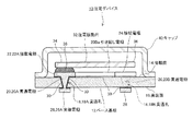
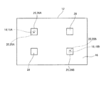
図1に、本実施形態の圧電デバイスの断面図を示す。また、図2に、本実施形態のベース基板の平面図を示し、図3に、本実施形態のベース基板の底面図を示す。 FIG. 1 shows a cross-sectional view of the piezoelectric device of the present embodiment. 2 shows a plan view of the base substrate of the present embodiment, and FIG. 3 shows a bottom view of the base substrate of the present embodiment.
本実施形態の圧電デバイス10(電子デバイス)は、ベース基板12と、ベース基板12に搭載される圧電振動片32と、ベース基板12に接合されるとともに圧電振動片32(電子部品)を気密封止するキャップ40と、により構成されている。
The piezoelectric device 10 (electronic device) of the present embodiment is bonded to the
圧電振動片32は、水晶等の圧電材料により形成され、音叉型振動片、双音叉型振動片、ATカット水晶基板による厚みすべり振動片、SAW共振片、ジャイロ振動片等を適用することができる。圧電振動片32は、基端34が導電性接着剤38によりベース基板12に接合されて固定端となり、先端36が自由端となり、片持ち支持状態でベース基板12に支持されている。
The piezoelectric vibrating
詳細は図示しないが、圧電振動片32の振動部には、振動部を固有の共振周波数で振動させる一対の励振電極が設けられている。また、各励振電極からは引出電極が引き出され、各引出電極は圧電振動片32の基端34の下面にまで延出している。
Although not shown in detail, the vibrating portion of the piezoelectric vibrating
ベース基板12は、セラミック等の絶縁基板により形成され、圧電振動片32を搭載する搭載面14と、搭載面14の裏面であって実装先の基板(不図示)に接合する実装面16と、を有する。
The
ベース基板12には、貫通孔18(図4(b)参照)が設けられている。貫通孔18(18A、18B)は、ベース基板12の厚み方向の断面形状が円形となる内壁を有し、搭載面14から実装面16までの間で、内径が単調に小さくなるテーパー形状の壁面を有している。よって、貫通孔18において、実装面16側の開口部の内径が搭載面14側の開口部の内径よりも小さくなっている。
The
この貫通孔18は、搭載面14側から研削用のレーザーの照射、あるいはサンドブラストにより形成される。レーザー照射及びサンドブラストは、ベース基板12の深さ方向のみならず、基板表面に平行な方向にもベース基板12の加工を進行させる。よって、レーザー照射及びサンドブラストを搭載面14側から行なうと、搭載面14側の方が実装面16側より前記平行な方向の加工が進行するので、結果的に実装面16側の内径が搭載面14側の内径よりも小さくなるテーパー形状の貫通孔18が形成される。
This through
本実施形態において貫通孔18は、平面視でベース基板12の対角線上の2箇所に設けられている。このうち、貫通孔18Aは、上述の引出電極(不図示)の真下となる位置に設けられている。また貫通孔18Bは、圧電振動片32の先端36側となる位置に設けられている。
In the present embodiment, the through
貫通孔18内には貫通電極20(20A,20B)が埋め込まれている。貫通電極20は、貫通孔18の内壁に倣って外形が形成され、搭載面14側及び実装面16側に露出している。よって、貫通電極20の実装面16に露出した部分の直径は、貫通電極20の搭載面14に露出した部分の直径よりも小さくなっている(図2、図3参照)。
A through electrode 20 (20A, 20B) is embedded in the through
ベース基板12の搭載面14には、搭載電極22(22A,22B)が設けられている。搭載電極22は、圧電振動片32の下面に引き出された引出電極(不図示)に対向する位置に設けられている。このうち、搭載電極22Aは、貫通電極20Aの搭載面14に露出した部分を覆うように設けられている。そして搭載電極22A上には、導電性接着剤38が塗布され、この導電性接着剤38が圧電振動片32の引出電極(不図示)の一方に接合することで、搭載電極22Aと引出電極(不図示)の一方とが電気的に接続される。
On the mounting
一方、貫通電極20Bの搭載面14に露出した位置には、接続電極24が設らけれている。そして、搭載電極22B(図2)からは、引き回し電極22Baが延出し接続電極24に接続している。搭載電極22B上には導電性接着剤38が塗布され、この導電性接着剤38が引出電極(不図示)の他方と接合することで、搭載電極22Bと引出電極(不図示)の他方とが電気的に接続される。
On the other hand, a
ベース基板12の実装面16の貫通電極20が露出した位置には実装電極26(26A、26B)が設けられている。実装電極26Aは、貫通電極20Aの実装面16に露出した部分を覆うように設けられ、実装電極26Bは、貫通電極20Bの実装面16に露出した部分を覆うように設けられている。しかし、貫通電極20の実装面16に露出した部分の直径は搭載面14に露出した部分より小さいので、実装電極26の寸法を小さく設計することができる。よって、ベース基板12の面積を小さくしても実装電極26の配置パターンの自由度を損なうことはない。
Mounting electrodes 26 (26A, 26B) are provided at positions where the through
実装電極26のうち、実装電極26Aは、貫通電極20A、搭載電極22A、及び導電性接着剤38を介して引出電極(不図示)の一方と電気的に接続する。一方、実装電極26B(図3)は、貫通電極20B、接続電極24、引き回し電極22Ba、搭載電極22B、及び導電性接着剤38を介して引出電極(不図示)の他方と電気的に接続する。したがって、実装電極26に交流電圧を印加することにより、圧電振動片32の振動部(不図示)は固有の共振周波数で振動する。
Of the mounting
実装電極26は、実装先の基板(不図示)に設けられた接続電極(不図示)に接合される。本実施形態では、実装電極26は実装面16に2つ設ければ十分であるが、実装先に安定的に接合させるため実装電極26と同一形状のダミー電極28が実装面16に設けられ、このダミー電極28を実装先の基板(不図示)の電極(不図示)に接合している。
The mounting
貫通孔18の内壁、搭載電極22の形成位置、実装電極26の形成位置等にはシード電極30が設けられている。シード電極30は、後述のようにスパッタ等により形成され、メッキ用の電極として用いられる。そして、シード電極30上に貫通電極20、搭載電極22、引き回し電極22Ba、接続電極24、及び実装電極26が成長している。なお、上記各種電極は、Cu(銅)等の伝導率の高い金属により形成されている。
A
キャップ40(蓋体)は、金属により形成され、下面が開口した凹部を有し、この凹部に圧電振動片32が収容可能となっている。キャップ40の下面を搭載面14に接合することにより、圧電振動片32を収容し、かつ圧電振動片32を気密封止(真空封止)する。
The cap 40 (lid body) is made of metal and has a recess having an open bottom surface, and the piezoelectric vibrating
なお、詳細は図示しないが、ベース基板12のダミー電極28に対応する位置に貫通電極を設け、貫通電極の搭載面14に露出した位置に接続電極を設け、この接続電極をキャップ40に接続するようにしてもよい。これにより、ダミー電極28を接地してキャップ40を接地させ、圧電振動片32に対する外部からの電気的な干渉を回避することができる。
Although not shown in detail, a through electrode is provided at a position corresponding to the
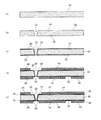
図4、図5に、本実施形態のベース基板の製造工程を示す。次に本実施形態のベース基板12の製造工程について説明する。図4(a)に示すように、ベース基板12と同一寸法の基板母材42を用意し、図4(b)に示すように、基板母材42の搭載面14となる側からレーザー照射またはサンドブラストによりテーパー形状の貫通孔18を形成する。
4 and 5 show the manufacturing process of the base substrate of this embodiment. Next, the manufacturing process of the
図4(c)に示すように、スパッタ等の方法を用いて基板母材42の表面にCu(銅)等の金属のシード電極30を形成する。このとき、貫通孔18はテーパー状に形成されているため、スパッタを用いても貫通孔18の内壁に容易にシード電極30を形成することができる。なお、図4(c)において、シード電極30は全て繋がっているものとする。
As shown in FIG. 4C, a
図4(d)に示すように、シード電極30上の貫通電極20、搭載電極22、引き回し電極22Ba(図4では不図示)、接続電極24(図4では不図示)、実装電極26、ダミー電極28に対応する位置を除いてレジスト膜44を形成する。
As shown in FIG. 4D, the through
図4(e)に示すように、シード電極30及びレジスト膜44を形成した基板母材42を、Cu(銅)等の金属メッキ材料の電解液に投入してシード電極30に電界を印加する。このときシード電極30は、電極形成部分以外の部分で露出させておき、その部分に電界印加用のケーブル(不図示)を接続しておく。すると、シード電極30が露出した部分で、電極材料が成長してゆく。図4(e)においては、貫通電極20を形成する電極材料は未だ厚みが薄いので、貫通電極20の搭載面14側及び実装面16側が未だ開口しており、実装電極26及び搭載電極22等は、未だ中央部に孔を有することになる。
As shown in FIG. 4E, the
図5(a)に示すように、電極材料の成長が進行すると、貫通電極20の実装面16側の開口した部分が塞がり、実装電極26の中央部にあった孔も塞がることになる。しかし、搭載電極22の中央部で開口した凹部46が残ることになる。
As shown in FIG. 5A, when the growth of the electrode material proceeds, the opening portion on the mounting
図5(b)に示すように、電極材料の成長が図5(a)の場合よりも進行すると、貫通孔18が貫通電極20を形成する電極材料により埋まり始め、凹部46の直径及び深さが小さくなっていく。
As shown in FIG. 5 (b), when the growth of the electrode material proceeds more than in the case of FIG. 5 (a), the through
図5(c)に示すように、電極材料の成長が図5(b)の場合よりも進行すると、貫通孔18が貫通電極20を形成する電極材料により完全に埋まり、凹部46も消滅する。
そして、図5(d)に示すように、レジスト膜44を除去し、図5(e)に示すように、シード電極30の電極材料が成長した部分以外の部分を、エッチング等を用いて除去することによりベース基板12が得られる。
As shown in FIG. 5C, when the growth of the electrode material proceeds more than in the case of FIG. 5B, the through
Then, as shown in FIG. 5D, the resist
ベース基板12の搭載電極22A,22Bに導電性接着剤38を塗布し、導電性接着剤38と引出電極(不図示)を接合する形で圧電振動片32をベース基板12に支持させ、真空環境下でキャップ40を搭載面14に接合することにより圧電デバイス10が得られる。
A
本実施形態のベース基板12の製造方法は、一回のメッキ工程で、貫通電極20、搭載電極22、引き回し電極22Ba、接続電極24、実装電極26、ダミー電極28を一体で形成することができる点が大きなメリットである。したがって、製造工程を増やすことなくこれらの電極を形成することができるのでコストを抑制することができる。さらに貫通電極20、搭載電極22、接続電極24、及び実装電極26は、一体で形成されるので電極間での接触抵抗が低減される。また、貫通孔18が上述のようにテーパー形状を有するため、貫通孔18の実装面16側が搭載面14側よりも早く埋まるので、少ないメッキ量で実装電極26の平坦性を確保して、高品質化を図ることができる。
In the method for manufacturing the
本実施形態では、貫通電極20が実装面16から搭載面14に向かって断面の直径が大きくなる形状を有している。よって、搭載面14とキャップ40により形成された内部空間が真空となっている場合は、貫通電極20が内部空間側に引き寄せられるとも思われる。
In the present embodiment, the through
しかし、本実施形態では、貫通電極20と実装電極26が一体に形成され、実装電極26が貫通電極20を支持する形となるので、貫通電極20が内部空間側に引き寄せられることはなく、内部空間の気密性が低下することはない。そして、搭載電極22、貫通電極20、実装電極26は、一体的に形成されているので、製造工程を削減してコストを抑制するとともに、各電極同士の間に界面は存在せず、界面を通じた気密破壊を回避することができる。
However, in the present embodiment, the through
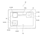
図6に、本実施形態の圧電デバイスの変形例の断面図を示し、図7に、本実施形態のベース基板の変形例の平面図を示す。変形例の圧電デバイス10A(電子デバイス)の基本構成は、図1の圧電デバイス10と共通するが、キャップ40の代わりに側壁部48とリッド52(蓋体)を用いている。側壁部48は、ベース基板12と同一の材料で形成され、矩形のリング形状を有している。そして、側壁部48の下面が搭載面14の周縁となる位置に接合されている。よって側壁部48の上面は搭載面14よりも高くなっており、側壁部48及び搭載面14により圧電振動片32を収容する凹部50が形成される。
FIG. 6 shows a cross-sectional view of a modification of the piezoelectric device of the present embodiment, and FIG. 7 shows a plan view of a modification of the base substrate of the present embodiment. The basic configuration of the piezoelectric device 10 </ b> A (electronic device) of the modification is common to the piezoelectric device 10 of FIG. 1, but uses a
リッド52は、金属により形成され、側壁部48の上面に接合して圧電振動片32を気密封止している。なお、側壁部48の上面に露出するとともに側壁部48及びベース基板12を連通し、ダミー電極28に接続する貫通電極(不図示)を形成し、リッド52を、ダミー電極28を介して接地できるようにしてもよい。
The
変形例の圧電デバイス10Aの組立は、搭載面14に側壁部48を接合し、圧電振動片32を搭載電極22A、22Bに接続したのちにリッド52を側壁部48に接合する工程となる。よって、圧電振動片32を側壁部48の内側(凹部50)に配置して、圧電振動片32の気密封止時に接触等により圧電振動片32を破損させる虞を回避することができる。
The assembly of the piezoelectric device 10 </ b> A according to the modification is a process of joining the
図8に、本実施形態の貫通孔の変形例の断面図を示し、図9に、本実施形態の貫通電極等の変形例の断面図を示す。本実施形態において、貫通孔18は、ベース基板12の厚み方向の全域にわたって壁面が傾斜したテーパー形状の壁面を有している。しかし、本発明における貫通孔は、ベース基板12の厚み方向の少なくとも一部において、その内径が搭載面14側よりも実装面16側の方が小さいテーパー形状の壁面を有していればよい。そして、実装面16側の開口部の内径が搭載面14側の開口部の内径よりも小さくなっていればよい。
FIG. 8 shows a cross-sectional view of a modified example of the through hole of the present embodiment, and FIG. 9 shows a cross-sectional view of a modified example of the through electrode of the present embodiment. In the present embodiment, the through
すなわち、変形例の貫通孔54のように、ベース基板12の搭載面14側に円筒形の壁面54aを有し、実装面16側においても円筒形の壁面54cを有し、壁面54a、54cとの間にテーパー形状の壁面54bを有するものしてもよい。
That is, like the through hole 54 of the modified example, the mounting
ベース基板12をセラミックで形成する場合、焼結前のベース基板12の焼結材料に型を用いて壁面54a、54cを壁面として有する2つの凹部を形成する。焼結材料を焼結させたのち、壁面54aからレーザー照射、またはサンドブラストにより壁面54aを有する凹部の底面から、壁面54cを有する凹部の底面までを貫通させ、壁面54aと壁面54cとの間に壁面54bを形成することにより貫通孔54を形成することができる。または、焼結前のベース基板12の焼結材料に型を用いて壁面54a、54b、54cを形成する型を押し付け、焼結材料を焼結させることにより貫通孔54を形成することもできる。
When the
図9に示すように、貫通孔54の壁面と貫通孔54を包含するベース基板12の両面の領域にシード電極30を配置し、シード電極30を用いたメッキにより貫通電極56、搭載電極22、実装電極26を一体的に形成することができる。なお、シード電極30をスパッタで形成する場合、スパッタのターゲットに対するベース基板12の向きをシード電極30の形成途中で変更させる等の制御を行なうことにより、壁面54a、54cへのシード電極30の形成が可能となる。また、スパッタのベース基板に対するメッキの成長過程は図4、図5と同様である。そして、一体的に形成された貫通電極56、搭載電極22、実装電極26の作用効果は、上述のように一体的に形成された貫通電極20、搭載電極22、実装電極26の作用効果と同様である。
As shown in FIG. 9, the
なお、本実施形態において、貫通電極20、搭載電極22、実装電極26を一体で形成する旨説明したが、電極間の接合強度を維持できる限り、または電極間の接触抵抗が無視できるほど小さい場合は、これらの電極を一体ではなく、別々の工程で形成してもよい。
In the present embodiment, it has been described that the through
10………圧電デバイス、12………ベース基板、14………搭載面、16………実装面、18,18A,18B………貫通孔、20………貫通電極、22,22A,22B………搭載電極、24………接続電極、26………実装電極、28………ダミー電極、30………シード電極、32………圧電振動片、34………基端、36………先端、38………導電性接着剤、40………キャップ、42………基板母材、44………レジスト膜、46………凹部、48………側壁部、50………凹部、52………リッド、54………貫通孔、56………貫通電極、100………圧電デバイス、102………ベース基板、104………キャップ、106………圧電振動片、108………貫通孔、110………貫通電極、112………搭載電極、114………導電性接着剤、200………圧電デバイス、202………貫通孔、204………電極、206………合金。
DESCRIPTION OF SYMBOLS 10 ......... Piezoelectric device, 12 ......... Base substrate, 14 ......... Mounting surface, 16 ......... Mounting surface, 18, 18A, 18B ......... Through hole, 20 ...... Through electrode, 22, 22A, 22B ......... Mounting electrode, 24 ......... Connecting electrode, 26 ......... Mounting electrode, 28 ......... Dummy electrode, 30 ......... Seed electrode, 32 ......... Piezoelectric vibrating piece, 34 ......... Base end, 36 ......... Tip, 38 ......... Conductive adhesive, 40 ......... Cap, 42 ......... Substrate base material, 44 ...... Resist film, 46 ......... Recess, 48 ......... Side wall, 50 ......... Recess, 52 ......... Lid, 54 ......... Through hole, 56 ......... Penetration electrode, 100 ......... Piezoelectric device, 102 ......... Base substrate, 104 ......... Cap, 106 .........
Claims (3)
前記貫通孔内に設ける貫通電極と、前記一方の面に電子部品を搭載するための搭載電極と、前記他方の面に設ける実装電極と、をメッキにより一体的に形成する工程と、
を含むことを特徴とするベース基板の製造方法。 A through-hole penetrating the insulating substrate, wherein at least a part of the through-hole in the thickness direction of the insulating substrate has a wall surface having a tapered shape with an inner diameter on the other surface side smaller than the one surface side of the insulating substrate Forming the through hole by forming an inner diameter of the opening on the other surface side smaller than an inner diameter of the opening on the one surface side; and
A step of integrally forming a through electrode provided in the through hole, a mounting electrode for mounting an electronic component on the one surface, and a mounting electrode provided on the other surface by plating ;
A method for manufacturing a base substrate, comprising:
前記電子部品を収容する蓋体を前記ベース基板に接合して、前記電子部品を封止する工程と、
を含むことを特徴とする電子デバイスの製造方法。 Disposing an electronic component on the mounting electrode on the base substrate manufactured by the manufacturing method according to claim 1 ,
Bonding the lid for housing the electronic component to the base substrate and sealing the electronic component;
The manufacturing method of the electronic device characterized by the above-mentioned.
Priority Applications (1)
| Application Number | Priority Date | Filing Date | Title |
|---|---|---|---|
| JP2012015338A JP5845929B2 (en) | 2012-01-27 | 2012-01-27 | Base substrate, electronic device, method for manufacturing base substrate, and method for manufacturing electronic device |
Applications Claiming Priority (1)
| Application Number | Priority Date | Filing Date | Title |
|---|---|---|---|
| JP2012015338A JP5845929B2 (en) | 2012-01-27 | 2012-01-27 | Base substrate, electronic device, method for manufacturing base substrate, and method for manufacturing electronic device |
Publications (3)
| Publication Number | Publication Date |
|---|---|
| JP2013157386A JP2013157386A (en) | 2013-08-15 |
| JP2013157386A5 JP2013157386A5 (en) | 2015-03-19 |
| JP5845929B2 true JP5845929B2 (en) | 2016-01-20 |
Family
ID=49052305
Family Applications (1)
| Application Number | Title | Priority Date | Filing Date |
|---|---|---|---|
| JP2012015338A Expired - Fee Related JP5845929B2 (en) | 2012-01-27 | 2012-01-27 | Base substrate, electronic device, method for manufacturing base substrate, and method for manufacturing electronic device |
Country Status (1)
| Country | Link |
|---|---|
| JP (1) | JP5845929B2 (en) |
Families Citing this family (2)
| Publication number | Priority date | Publication date | Assignee | Title |
|---|---|---|---|---|
| JP6341245B2 (en) * | 2016-09-05 | 2018-06-13 | 大日本印刷株式会社 | Penetration electrode substrate manufacturing method, penetration electrode substrate, and semiconductor device |
| JP6369653B1 (en) * | 2018-05-17 | 2018-08-08 | 大日本印刷株式会社 | Through electrode substrate and semiconductor device |
Family Cites Families (5)
| Publication number | Priority date | Publication date | Assignee | Title |
|---|---|---|---|---|
| JP4630110B2 (en) * | 2005-04-05 | 2011-02-09 | パナソニック株式会社 | Manufacturing method of electronic parts |
| JP5135510B2 (en) * | 2008-02-18 | 2013-02-06 | セイコーインスツル株式会社 | Piezoelectric vibrator manufacturing method, piezoelectric vibrator, oscillator, electronic device, and radio timepiece |
| WO2009104314A1 (en) * | 2008-02-18 | 2009-08-27 | セイコーインスツル株式会社 | Method for fabricating piezoeledctric vibrator, piezoeledctric vibrator, oscillator, electronic apparatus and radio-controlled clock |
| JP5143688B2 (en) * | 2008-09-26 | 2013-02-13 | シチズンファインテックミヨタ株式会社 | Method for manufacturing piezoelectric device |
| JP4843012B2 (en) * | 2008-11-17 | 2011-12-21 | 日本電波工業株式会社 | Piezoelectric device and manufacturing method thereof |
-
2012
- 2012-01-27 JP JP2012015338A patent/JP5845929B2/en not_active Expired - Fee Related
Also Published As
| Publication number | Publication date |
|---|---|
| JP2013157386A (en) | 2013-08-15 |
Similar Documents
| Publication | Publication Date | Title |
|---|---|---|
| JP2007005948A (en) | Electronic component and manufacturing method thereof | |
| JP2013098209A (en) | Circuit board, electronic device, electronic equipment, and circuit board manufacturing method | |
| JP5845929B2 (en) | Base substrate, electronic device, method for manufacturing base substrate, and method for manufacturing electronic device | |
| JP2006332727A (en) | Piezoelectric device | |
| JP5278044B2 (en) | Package member, method for manufacturing the package member, and piezoelectric vibration device using the package member | |
| JP4122512B2 (en) | Piezoelectric vibration device | |
| JP5239784B2 (en) | Piezoelectric vibration device | |
| JP2013162295A (en) | Base substrate, electronic device, manufacturing method of base substrate, and manufacturing method of electronic device | |
| JP2006042096A (en) | Package for storing piezoelectric element, piezoelectric device, and manufacture of the device | |
| JP5376490B2 (en) | Manufacturing method of electronic component package | |
| JP6482282B2 (en) | Electronic components | |
| JP2017038227A (en) | Electronic component and manufacturing method therefor | |
| JP2007324957A (en) | Piezoelectric vibrator | |
| JP2002076817A (en) | Piezoelectric vibration device | |
| JP2005217801A (en) | Piezoelectric transducer | |
| JP4461953B2 (en) | Piezoelectric vibration device | |
| JP2001127576A (en) | Structure for package for piezoelectric vibrator and its manufacture | |
| JP2007208470A (en) | Piezoelectric vibrator | |
| JP2001352225A (en) | Hermetic seal structure of quartz oscillator | |
| JP2011205391A (en) | Electronic component package, and piezoelectric vibration device employing the electronic component package | |
| JP2010154191A (en) | Piezoelectric device for surface mounting | |
| JP2009111931A (en) | Piezoelectric vibrator and method for manufacturing piezoelectric vibrator | |
| JP2007142947A (en) | Surface-mounting piezoelectric oscillator | |
| JP6449620B2 (en) | Quartz crystal resonator and manufacturing method thereof | |
| JP2005184325A (en) | Quartz oscillator |
Legal Events
| Date | Code | Title | Description |
|---|---|---|---|
| A521 | Request for written amendment filed |
Free format text: JAPANESE INTERMEDIATE CODE: A523 Effective date: 20150126 |
|
| A621 | Written request for application examination |
Free format text: JAPANESE INTERMEDIATE CODE: A621 Effective date: 20150126 |
|
| A131 | Notification of reasons for refusal |
Free format text: JAPANESE INTERMEDIATE CODE: A131 Effective date: 20150701 |
|
| A521 | Request for written amendment filed |
Free format text: JAPANESE INTERMEDIATE CODE: A523 Effective date: 20150804 |
|
| A131 | Notification of reasons for refusal |
Free format text: JAPANESE INTERMEDIATE CODE: A131 Effective date: 20150908 |
|
| A521 | Request for written amendment filed |
Free format text: JAPANESE INTERMEDIATE CODE: A523 Effective date: 20150930 |
|
| TRDD | Decision of grant or rejection written | ||
| A01 | Written decision to grant a patent or to grant a registration (utility model) |
Free format text: JAPANESE INTERMEDIATE CODE: A01 Effective date: 20151027 |
|
| A61 | First payment of annual fees (during grant procedure) |
Free format text: JAPANESE INTERMEDIATE CODE: A61 Effective date: 20151109 |
|
| R150 | Certificate of patent or registration of utility model |
Ref document number: 5845929 Country of ref document: JP Free format text: JAPANESE INTERMEDIATE CODE: R150 |
|
| S531 | Written request for registration of change of domicile |
Free format text: JAPANESE INTERMEDIATE CODE: R313531 |
|
| R350 | Written notification of registration of transfer |
Free format text: JAPANESE INTERMEDIATE CODE: R350 |
|
| LAPS | Cancellation because of no payment of annual fees |