JP5843624B2 - Power conversion system for grid connection - Google Patents
Power conversion system for grid connection Download PDFInfo
- Publication number
- JP5843624B2 JP5843624B2 JP2012006659A JP2012006659A JP5843624B2 JP 5843624 B2 JP5843624 B2 JP 5843624B2 JP 2012006659 A JP2012006659 A JP 2012006659A JP 2012006659 A JP2012006659 A JP 2012006659A JP 5843624 B2 JP5843624 B2 JP 5843624B2
- Authority
- JP
- Japan
- Prior art keywords
- power
- converter
- power supply
- power source
- semiconductor switch
- Prior art date
- Legal status (The legal status is an assumption and is not a legal conclusion. Google has not performed a legal analysis and makes no representation as to the accuracy of the status listed.)
- Expired - Fee Related
Links
Images


Classifications
-
- Y—GENERAL TAGGING OF NEW TECHNOLOGICAL DEVELOPMENTS; GENERAL TAGGING OF CROSS-SECTIONAL TECHNOLOGIES SPANNING OVER SEVERAL SECTIONS OF THE IPC; TECHNICAL SUBJECTS COVERED BY FORMER USPC CROSS-REFERENCE ART COLLECTIONS [XRACs] AND DIGESTS
- Y02—TECHNOLOGIES OR APPLICATIONS FOR MITIGATION OR ADAPTATION AGAINST CLIMATE CHANGE
- Y02E—REDUCTION OF GREENHOUSE GAS [GHG] EMISSIONS, RELATED TO ENERGY GENERATION, TRANSMISSION OR DISTRIBUTION
- Y02E60/00—Enabling technologies; Technologies with a potential or indirect contribution to GHG emissions mitigation
- Y02E60/10—Energy storage using batteries
-
- Y—GENERAL TAGGING OF NEW TECHNOLOGICAL DEVELOPMENTS; GENERAL TAGGING OF CROSS-SECTIONAL TECHNOLOGIES SPANNING OVER SEVERAL SECTIONS OF THE IPC; TECHNICAL SUBJECTS COVERED BY FORMER USPC CROSS-REFERENCE ART COLLECTIONS [XRACs] AND DIGESTS
- Y02—TECHNOLOGIES OR APPLICATIONS FOR MITIGATION OR ADAPTATION AGAINST CLIMATE CHANGE
- Y02E—REDUCTION OF GREENHOUSE GAS [GHG] EMISSIONS, RELATED TO ENERGY GENERATION, TRANSMISSION OR DISTRIBUTION
- Y02E60/00—Enabling technologies; Technologies with a potential or indirect contribution to GHG emissions mitigation
- Y02E60/30—Hydrogen technology
- Y02E60/36—Hydrogen production from non-carbon containing sources, e.g. by water electrolysis
-
- Y—GENERAL TAGGING OF NEW TECHNOLOGICAL DEVELOPMENTS; GENERAL TAGGING OF CROSS-SECTIONAL TECHNOLOGIES SPANNING OVER SEVERAL SECTIONS OF THE IPC; TECHNICAL SUBJECTS COVERED BY FORMER USPC CROSS-REFERENCE ART COLLECTIONS [XRACs] AND DIGESTS
- Y02—TECHNOLOGIES OR APPLICATIONS FOR MITIGATION OR ADAPTATION AGAINST CLIMATE CHANGE
- Y02E—REDUCTION OF GREENHOUSE GAS [GHG] EMISSIONS, RELATED TO ENERGY GENERATION, TRANSMISSION OR DISTRIBUTION
- Y02E70/00—Other energy conversion or management systems reducing GHG emissions
- Y02E70/30—Systems combining energy storage with energy generation of non-fossil origin
Description
この発明は、交流系統電源を含む複数の電源から電機負荷へ電力供給を行う系統連系用電力変換システムに関する。 The present invention relates to a grid interconnection power conversion system that supplies power to an electric load from a plurality of power supplies including an AC grid power supply.
従来の系統連系用電力変換システムには、交流系統電源、電機負荷、太陽電池、および蓄電池の相互間に電力変換器を介在し、電機負荷への電力供給や電源間の電力融通を行う構成のものが提案されている(例えば、特許文献1参照)。 The conventional grid-connected power conversion system has a configuration in which a power converter is interposed between an AC system power supply, an electric load, a solar battery, and a storage battery, and power is supplied to the electric load and power is interchanged between the power supplies. Have been proposed (see, for example, Patent Document 1).
すなわち、上記の特許文献1記載の従来技術では、交流直流双方向コンバータの交流側には交流系統電源と電機負荷とを共に接続する一方、交流直流双方向コンバータの直流側には太陽電池と並列に、第1の蓄電池および電気自動車に搭載された自動車用の第2の蓄電池を共に接続し、太陽電池から直接に第1と第2の蓄電池に電力を充電すること、また、太陽電池と第1、第2の蓄電池の電力を用いて交流系統電源への回生電力を供給したり、電機負荷への電力供給を行うようにしている。
That is, in the prior art described in
上記の特許文献1記載の従来技術では、次の課題がある。すなわち、(1)電機負荷を交流系統電源に並列に接続しているため、交流系統電源の電圧と異なる電圧仕様の電機負荷を接続することができない。(2)また、電力変換器が車外に設置されるため、電機負荷を接続して使用する場所が電力変換器が設置された付近に限られ、任意の場所で電機負荷を接続することができない。(3)さらに、各種電源から電機負荷への電力供給時、または電源間の電力融通について、使用する電源の優先順位が定められていないため、例えば交流系統電源の停電や太陽電池の発電電力不足などが起こるなどの非常時により、第1、第2の蓄電池のみで電機負荷へ電力を供給する必要が発生した場合に、これらの第1、第2の蓄電池の充電量が最適に保持されず、電機負荷への電力供給の信頼性が低下する恐れがある。
The conventional technique described in
この発明の系統連系用電力変換システムは、第1〜第4の接続部が設けられた電力変換器を備え、上記電力変換器は、直流母線相互間を接続する直流リンク部と、交流系統電源と上記直流リンク部の間を接続するAC/DCコンバータと、電機負荷と上記直流リンク部の間を接続するDC/ACインバータとを備え、上記AC/DCコンバータと上記DC/ACインバータを共に4つの半導体スイッチ素子からなるフルブリッジ回路で構成とするとともに、上記AC/DCコンバータと上記DC/ACインバータの1アームを共通化し、この共通化した1アームを構成する2つの半導体スイッチ素子間の接続点を上記電機負荷のN母線側の端子に接続しており、上記DC/ACインバータの上記共通化した1アームを構成する2つの半導体スイッチ素子の内、N母線側の半導体スイッチ素子をONに固定するとともに、他方の1アームを構成する2つの半導体スイッチ素子をスイッチングして上記電機負荷へ直流電圧を供給するものである。
あるいは、上記電力変換器は、直流母線相互間を接続する直流リンク部と、交流系統電源と上記直流リンク部の間を接続するAC/DCコンバータと、電機負荷と上記直流リンク部の間を接続するDC/ACインバータとを備え、上記AC/DCコンバータを4つの半導体スイッチ素子からなるフルブリッジ回路で、上記DC/ACインバータを2つの半導体スイッチ素子からなるハーフブリッジ回路でそれぞれ構成し、また上記直流リンク部を2つのコンデンサを直列接続して構成するとともに、上記直流リンク部の両コンデンサの中性点を接地し、上記ハーフブリッジ回路を構成する2つの半導体スイッチ素子間の接続点を上記電機負荷のP母線側の端子に接続している。
そして、上記電力変換器の上記第1の接続部には上記交流系統電源が、上記第2の接続部には発電のみを行う発電用直流電源が、上記第3の接続部には充放電可能な充放電用直流電源が、上記第4の接続部には上記電機負荷がそれぞれ接続された状態において、上記交流系統電源と上記発電用直流電源を主電源として上記電機負荷へ電力を供給する場合に、上記発電用直流電源の発電電力を最大値に固定し、上記発電用直流電源の発電電力が上記電機負荷が必要な電力より少ない場合には、その不足電力を上記充放電用直流電源よりも上記交流系統電源を優先して上記電機負荷へ供給する一方、上記発電用直流電源の発電電力が上記電機負荷が必要な電力よりも多い場合には、その余剰電力により上記充放電用直流電源を充電する。
The power conversion system for grid interconnection of this invention is equipped with the power converter provided with the 1st-4th connection part, The said power converter, The direct current | flow link part which connects between direct current buses, and an alternating current system An AC / DC converter that connects a power source and the DC link unit, and a DC / AC inverter that connects an electrical load and the DC link unit, both the AC / DC converter and the DC / AC inverter A full bridge circuit composed of four semiconductor switch elements is used, and one arm of the AC / DC converter and the DC / AC inverter is shared, and between the two semiconductor switch elements constituting the shared one arm. The connection point is connected to the terminal on the N bus side of the electric load, and two semiconductor devices constituting the common one arm of the DC / AC inverter are connected. Among pitch element, to fix the semiconductor switch device N bus side to ON, and supplies the DC voltage to the electrical load by switching the two semiconductor switching elements constituting the other of the arm.
Alternatively, the power converter connects a direct current link between the direct current buses, an AC / DC converter that connects between the alternating current system power supply and the direct current link, and an electrical load and the direct current link. The AC / DC converter is a full bridge circuit composed of four semiconductor switch elements, and the DC / AC inverter is composed of a half bridge circuit composed of two semiconductor switch elements. The DC link unit is configured by connecting two capacitors in series, the neutral point of both capacitors of the DC link unit is grounded, and the connection point between the two semiconductor switch elements forming the half bridge circuit is the electric machine. It is connected to the terminal on the P bus side of the load.
Then, the above AC system power source to the first connection portion of the power converter, the second power generating DC power source to perform only power in the connecting portion, the third to the connection portion rechargeable If Do discharge DC power supply is to supply the state to the fourth connecting portion where the electric load is connected respectively, the power to the electric load the AC system power source and a DC power source for the generator as a main power source In addition, when the generated power of the DC power source for power generation is fixed to the maximum value and the generated power of the DC power source for power generation is less than the power required for the electrical load, the shortage power is reduced from the DC power source for charging / discharging. In addition, the AC power supply is preferentially supplied to the electric load, and when the generated power of the DC power supply for generation is greater than the electric power required for the electric load, the surplus power is used to supply the charge / discharge DC power supply. you charge.
また、この発明の系統連系用電力変換システムは、第1〜第4の接続部が設けられた電力変換器を備え、上記電力変換器は、直流母線相互間を接続する直流リンク部と、交流系統電源と上記直流リンク部の間を接続するAC/DCコンバータと、電機負荷と上記直流リンク部の間を接続するDC/ACインバータとを備え、上記AC/DCコンバータと上記DC/ACインバータを共に4つの半導体スイッチ素子からなるフルブリッジ回路で構成とするとともに、上記AC/DCコンバータと上記DC/ACインバータの1アームを共通化し、この共通化した1アームを構成する2つの半導体スイッチ素子間の接続点を上記電機負荷のN母線側の端子に接続しており、上記DC/ACインバータの上記共通化した1アームを構成する2つの半導体スイッチ素子の内、N母線側の半導体スイッチ素子をONに固定するとともに、他方の1アームを構成する2つの半導体スイッチ素子をスイッチングして上記電機負荷へ直流電圧を供給するものである。
あるいは、上記電力変換器は、直流母線相互間を接続する直流リンク部と、交流系統電源と上記直流リンク部の間を接続するAC/DCコンバータと、電機負荷と上記直流リンク部の間を接続するDC/ACインバータとを備え、上記AC/DCコンバータを4つの半導体スイッチ素子からなるフルブリッジ回路で、上記DC/ACインバータを2つの半導体スイッチ素子からなるハーフブリッジ回路でそれぞれ構成し、また上記直流リンク部を2つのコンデンサを直列接続して構成するとともに、上記直流リンク部の両コンデンサの中性点を接地し、上記ハーフブリッジ回路を構成する2つの半導体スイッチ素子間の接続点を上記電機負荷のP母線側の端子に接続している。
そして、上記電力変換器の上記第1の接続部には上記交流系統電源が接続されず、上記第2の接続部には発電のみを行う発電用直流電源が、上記第3の接続部には充放電可能な充放電用直流電源が、上記第4の接続部には上記電機負荷がそれぞれ接続された状態において、上記発電用直流電源を主電源として上記電機負荷に電力を供給する場合に、上記発電用直流電源の発電電力を最大値に固定し、上記発電用直流電源の発電電力が上記電機負荷が必要とする電力量より多い場合には、その余剰電力により上記充放電用直流電源を充電し、上記充放電用直流電源が満充電に達したならば上記発電用直流電源の発電電力を上記電機負荷が必要とする電力まで減少させる。
The grid interconnection power conversion system of the present invention includes a power converter provided with first to fourth connection portions, and the power converter includes a DC link unit that connects between DC buses, and An AC / DC converter that connects between an AC system power supply and the DC link unit, and a DC / AC inverter that connects an electric load and the DC link unit, the AC / DC converter and the DC / AC inverter Are constituted by a full bridge circuit composed of four semiconductor switch elements, and one arm of the AC / DC converter and the DC / AC inverter is shared, and two semiconductor switch elements constituting the shared one arm Is connected to the terminal on the N bus side of the electric load, and the two half points constituting the common one arm of the DC / AC inverter are connected. Among the body switch element, as well as fix the semiconductor switching element of N bus side to ON, and supplies the DC voltage to the electrical load by switching the two semiconductor switching elements constituting the other of the arm.
Alternatively, the power converter connects a direct current link between the direct current buses, an AC / DC converter that connects between the alternating current system power supply and the direct current link, and an electrical load and the direct current link. The AC / DC converter is a full bridge circuit composed of four semiconductor switch elements, and the DC / AC inverter is composed of a half bridge circuit composed of two semiconductor switch elements. The DC link unit is configured by connecting two capacitors in series, the neutral point of both capacitors of the DC link unit is grounded, and the connection point between the two semiconductor switch elements forming the half bridge circuit is the electric machine. It is connected to the terminal on the P bus side of the load.
Then, to the first connecting portion of the power converter is not the AC system power source is connected, the second power generating DC power source connection section that generates power only, to the third connecting portion when rechargeable discharge DC power supply is above the fourth connection portion for supplying in a state where the electric load is connected respectively, the power to the electric load DC power for the generator as a main power source, When the generated power of the DC power source for power generation is fixed to the maximum value and the generated power of the DC power source for power generation is larger than the amount of power required by the electrical load, the DC power source for charging and discharging is reduced by the surplus power. charge, Ru reduced if the charge and discharge DC power supply has reached a full charge generated power for the generator the DC power source to power the electric load requires.
また、この発明の系統連系用電力変換システムは、第1〜第4の接続部が設けられた電力変換器を備え、上記電力変換器は、直流母線相互間を接続する直流リンク部と、交流系統電源と上記直流リンク部の間を接続するAC/DCコンバータと、電機負荷と上記直流リンク部の間を接続するDC/ACインバータとを備え、上記AC/DCコンバータと上記DC/ACインバータを共に4つの半導体スイッチ素子からなるフルブリッジ回路で構成とするとともに、上記AC/DCコンバータと上記DC/ACインバータの1アームを共通化し、この共通化した1アームを構成する2つの半導体スイッチ素子間の接続点を上記電機負荷のN母線側の端子に接続しており、上記DC/ACインバータの上記共通化した1アームを構成する2つの半導体スイッチ素子の内、N母線側の半導体スイッチ素子をONに固定するとともに、他方の1アームを構成する2つの半導体スイッチ素子をスイッチングして上記電機負荷へ直流電圧を供給するものである。
あるいは、上記電力変換器は、直流母線相互間を接続する直流リンク部と、交流系統電源と上記直流リンク部の間を接続するAC/DCコンバータと、電機負荷と上記直流リンク部の間を接続するDC/ACインバータとを備え、上記AC/DCコンバータを4つの半導体スイッチ素子からなるフルブリッジ回路で、上記DC/ACインバータを2つの半導体スイッチ素子からなるハーフブリッジ回路でそれぞれ構成し、また上記直流リンク部を2つのコンデンサを直列接続して構成するとともに、上記直流リンク部の両コンデンサの中性点を接地し、上記ハーフブリッジ回路を構成する2つの半導体スイッチ素子間の接続点を上記電機負荷のP母線側の端子に接続している。
そして、上記電力変換器の上記第1の接続部には上記交流系統電源が、上記第2の接続部には発電のみを行う発電用直流電源が、上記第3の接続部には充放電可能な充放電用直流電源が、上記第4の接続部には上記電機負荷がそれぞれ接続された状態において、上記発電用直流電源を主電源として上記電機負荷と上記充放電用直流電源とを共に負荷と見なして電力供給を行う場合に、上記発電用直流電源の発電電力を最大値に、上記充放電用直流電源を所定の充電電力値にそれぞれ固定し、上記発電用直流電源の発電電力が上記電機負荷と上記充放電用直流電源への必要電力の総和より少ない場合には、その不足電力を上記交流系統電源から供給する一方、上記発電用直流電源の発電電力が上記電機負荷と上記充放電用直流電源への必要電力の総和よりも多い場合には、その余剰電力を上記交流系統電源に回生する。
The grid interconnection power conversion system of the present invention includes a power converter provided with first to fourth connection portions, and the power converter includes a DC link unit that connects between DC buses, and An AC / DC converter that connects between an AC system power supply and the DC link unit, and a DC / AC inverter that connects an electric load and the DC link unit, the AC / DC converter and the DC / AC inverter Are constituted by a full bridge circuit composed of four semiconductor switch elements, and one arm of the AC / DC converter and the DC / AC inverter is shared, and two semiconductor switch elements constituting the shared one arm Is connected to the terminal on the N bus side of the electric load, and the two half points constituting the common one arm of the DC / AC inverter are connected. Among the body switch element, as well as fix the semiconductor switching element of N bus side to ON, and supplies the DC voltage to the electrical load by switching the two semiconductor switching elements constituting the other of the arm.
Alternatively, the power converter connects a direct current link between the direct current buses, an AC / DC converter that connects between the alternating current system power supply and the direct current link, and an electrical load and the direct current link. The AC / DC converter is a full bridge circuit composed of four semiconductor switch elements, and the DC / AC inverter is composed of a half bridge circuit composed of two semiconductor switch elements. The DC link unit is configured by connecting two capacitors in series, the neutral point of both capacitors of the DC link unit is grounded, and the connection point between the two semiconductor switch elements forming the half bridge circuit is the electric machine. It is connected to the terminal on the P bus side of the load.
Then, the above AC system power source to the first connection portion of the power converter, the second power generating DC power source to perform only power in the connecting portion, the third to the connection portion rechargeable Do discharge DC power supply is in a state above the fourth connecting portion where the electrical load is connected, the electric load and the charging and discharging DC power supply and together load DC power for the generator as a main power source When the power supply is performed assuming that the power generation power of the power generation DC power source is fixed to a maximum value, the charge / discharge DC power source is fixed to a predetermined charge power value, and the power generation power of the power generation DC power source is If the total power required for the electrical load and the charging / discharging DC power supply is less than the sum, the shortage power is supplied from the AC system power supply, while the generated power of the generating DC power supply is the electrical load and the charging / discharging. Power required for DC power supply If greater than the sum is it regenerating the excess power to the AC system power source.
また、この発明の系統連系用電力変換システムは、第1〜第4の接続部が設けられた電力変換器を備え、上記電力変換器は、直流母線相互間を接続する直流リンク部と、交流系統電源と上記直流リンク部の間を接続するAC/DCコンバータと、電機負荷と上記直流リンク部の間を接続するDC/ACインバータとを備え、上記AC/DCコンバータと上記DC/ACインバータを共に4つの半導体スイッチ素子からなるフルブリッジ回路で構成とするとともに、上記AC/DCコンバータと上記DC/ACインバータの1アームを共通化し、この共通化した1アームを構成する2つの半導体スイッチ素子間の接続点を上記電機負荷のN母線側の端子に接続しており、上記DC/ACインバータの上記共通化した1アームを構成する2つの半導体スイッチ素子の内、N母線側の半導体スイッチ素子をONに固定するとともに、他方の1アームを構成する2つの半導体スイッチ素子をスイッチングして上記電機負荷へ直流電圧を供給するものである。
あるいは、上記電力変換器は、直流母線相互間を接続する直流リンク部と、交流系統電源と上記直流リンク部の間を接続するAC/DCコンバータと、電機負荷と上記直流リンク部の間を接続するDC/ACインバータとを備え、上記AC/DCコンバータを4つの半導体スイッチ素子からなるフルブリッジ回路で、上記DC/ACインバータを2つの半導体スイッチ素子からなるハーフブリッジ回路でそれぞれ構成し、また上記直流リンク部を2つのコンデンサを直列接続して構成するとともに、上記直流リンク部の両コンデンサの中性点を接地し、上記ハーフブリッジ回路を構成する2つの半導体スイッチ素子間の接続点を上記電機負荷のP母線側の端子に接続している。
そして、上記電力変換器の上記第1の接続部には上記交流系統電源が、上記第2の接続部には発電のみを行う発電用直流電源が、上記第3の接続部には充放電可能な充放電用直流電源が、上記第4の接続部には上記電機負荷がそれぞれ接続された状態において、上記発電用直流電源を主電源として上記電機負荷と上記交流系統電源を共に負荷と見なして電力供給を行う場合に、上記充放電用直流電源の充電量が満充電でない場合において、上記発電用直流電源の発電電力を最大値に固定し、上記発電用直流電源の発電電力が上記電機負荷の必要電力と上記交流系統電源の回生電力の総和より少ない場合には、上記交流系統電源のみで電力不足分だけ電力回生量を減少させる一方、上記発電用直流電源の発電電力が上記電機負荷の必要電力と上記交流系統電源の回生電力の総和より多い場合には、上記電機負荷の必要電力と上記充放電用直流電源の必要充電量の総和と上記発電用直流電源の発電電力との差電力を上記交流系統電源へ回生する。
The grid interconnection power conversion system of the present invention includes a power converter provided with first to fourth connection portions, and the power converter includes a DC link unit that connects between DC buses, and An AC / DC converter that connects between an AC system power supply and the DC link unit, and a DC / AC inverter that connects an electric load and the DC link unit, the AC / DC converter and the DC / AC inverter Are constituted by a full bridge circuit composed of four semiconductor switch elements, and one arm of the AC / DC converter and the DC / AC inverter is shared, and two semiconductor switch elements constituting the shared one arm Is connected to the terminal on the N bus side of the electric load, and the two half points constituting the common one arm of the DC / AC inverter are connected. Among the body switch element, as well as fix the semiconductor switching element of N bus side to ON, and supplies the DC voltage to the electrical load by switching the two semiconductor switching elements constituting the other of the arm.
Alternatively, the power converter connects a direct current link between the direct current buses, an AC / DC converter that connects between the alternating current system power supply and the direct current link, and an electrical load and the direct current link. The AC / DC converter is a full bridge circuit composed of four semiconductor switch elements, and the DC / AC inverter is composed of a half bridge circuit composed of two semiconductor switch elements. The DC link unit is configured by connecting two capacitors in series, the neutral point of both capacitors of the DC link unit is grounded, and the connection point between the two semiconductor switch elements forming the half bridge circuit is the electric machine. It is connected to the terminal on the P bus side of the load.
Then, the above AC system power source to the first connection portion of the power converter, the second power generating DC power source to perform only power in the connecting portion, the third to the connection portion rechargeable Do discharge DC power supply is in a state to the fourth connection portion is the electrical load is connected, the DC power supply for the power generation is regarded as the electric load and the AC system power source together load as the main power source When supplying power, if the charge amount of the charge / discharge DC power supply is not fully charged, the generated power of the DC power supply for power generation is fixed to the maximum value, and the generated power of the DC power supply for power generation is If the total power required is less than the sum of the regenerative power of the AC system power supply, the power regeneration amount is reduced by the shortage of power only with the AC system power supply, while the generated power of the DC power supply for power generation Power requirements and above If the sum of the regenerative power of the AC system power supply is greater than the sum of the regenerative power of the AC system power supply, the difference power between the sum of the required power of the electrical load and the required charge amount of the charge / discharge DC power supply and the generated power of the DC power supply for power generation is calculated. It regenerated to the power supply.
この発明の系統連系用電力変換システムは、電力変換器に4つの接続部を備えているため、交流系統電源と電機負荷との間に電力変換器を介した構成となり、交流系統電源と異なる電圧定格の電機負荷を接続しても継続的に使用することができる。また発電用直流電源の電力を最大に発電して最優先して電力供給を行うことで、経済的にも資源的にも効率的に電機機器へ電力を供給することができる。さらに、充放電用直流電源の電力使用の優先度を下げて蓄電の優先度を上げることで、充放電用直流電源の充電量をより増加させる運用方法となり、例えば交流系統電源の停電や太陽電池の発電電力不足などが起こるなどの非常時での電機機器への電力供給の信頼性をより向上させることができる。 Since the power conversion system for grid connection of the present invention includes four connections in the power converter, the power converter is provided between the AC system power supply and the electric load, and is different from the AC system power supply. Even if a voltage rated electrical load is connected, it can be used continuously. Further, by generating the maximum power from the DC power supply for power generation and supplying power with the highest priority, it is possible to efficiently supply power to the electrical equipment both economically and in resources. Furthermore, by lowering the power usage priority of the DC power supply for charging / discharging and increasing the power storage priority, it becomes an operation method for further increasing the charge amount of the DC power supply for charging / discharging, such as a power failure or solar battery of an AC system power supply. Therefore, it is possible to further improve the reliability of power supply to the electrical equipment in an emergency such as a shortage of generated power.
実施の形態1.
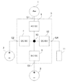
図1はこの実施の形態1における系統連系用電力変換システムの全体を示す構成図である。
FIG. 1 is a configuration diagram showing the entire grid interconnection power conversion system according to the first embodiment.
この実施の形態1の系統連系用電力変換システムは、電力変換器5を有し、この電力変換器5は4つの接続部G1〜G4を備え、第1の接続部G1には交流系統電源1が、第2の接続部G2には発電用直流電源2が、第3の接続部G3には充放電用直流電源3が、第4の接続部G4には交流の電機負荷4がそれぞれ接続されている。
The grid interconnection power conversion system according to the first embodiment includes a
ここに、電力変換器5は、EV、PHEV、HEVなどの電動自動車に搭載される車載用のものであり、そのため、電機負荷4は車で移動できる範囲で自由に使用することができる。これは非常時などの可搬型電源として大いに利用価値が向上する。
Here, the
また、交流系統電源1は一般の商用電源であり、ここでは国内の単相2線式、あるいは単相3線式を想定している。発電用直流電源2は、例えば風力発電、太陽光パネル、NAS電池、燃料電池など発電のみを行う直流電源がこれに該当する。また、充放電用直流電源3は、電気自動車を駆動するための高圧バッテリ、または車内電装品を動作させるための低圧バッテリ、例えばリチウムイオンバッテリ、鉛バッテリ、ニッケル水素バッテリ、EDLC、電解コンデンサなど充放電可能な直流電源がこれに該当する。
The AC
電力変換器5は、直流母線相互間を接続する直流リンク部10を備えるとともに、交流系統電源1と直流リンク部10との間で電力変換を行うAC/DCコンバータ6、発電用直流電源2と直流リンク部10との間で電力変換を行う第1のDC/DCコンバータ7、充放電用直流電源3と直流リンク部10との間で電力変換を行う第2のDC/DCコンバータ9、および交流の電機負荷4と直流リンク部10との間で電力変換を行うDC/ACインバータ8を有する。
The
上記のAC/DCコンバータ6は、交流電圧を直流電圧に又は直流電圧を交流電圧に変換するもので、電力伝送は交流系統電源1から直流リンク部10、または直流リンク部10から交流系統電源1の双方向に電力伝送するように構成されている。また、上記の第1のDC/DCコンバータ7は、発電用直流電源2から直流リンク部10に向かってのみ電力伝送するように構成されている。また、上記の第2のDC/DCコンバータ9は、直流リンク部10から充放電用直流電源3、または充放電用直流電源3から直流リンク部10の双方向に電力伝送するように構成されている。さらに、上記のDC/ACインバータ8は、直流電圧を交流電圧に変換するもので、直流リンク部10から交流の電機負荷4に電力伝送する。その場合、DC/ACインバータ8のAC出力電圧は、これに接続される電機負荷4の定格交流電圧に合わせて調整することができるようになっている。
The AC /
このような構成をとることで、電機負荷4には、交流系統電源1、発電用直流電源2、充放電用直流電源の3つの電源が電力変換器5を介して接続されるため、電機負荷4の電圧定格に合わせて電力変換器5は任意の電圧を出力することができる。
By adopting such a configuration, the
図2は同系統連系用電力変換システムが備える電力変換器の制御系を示す構成図である。 FIG. 2 is a configuration diagram illustrating a control system of a power converter included in the grid interconnection power conversion system.
この実施の形態1では、各電源1〜3の電圧、電流、位相などをセンシングし、各直流電源2、3や交流系統電源1への供給電力や回生電力を演算する。そのため、交流系統電源1の電圧、電流、位相の各センサ値をAC/DCコンバータ6の交流側でセンシングして制御回路15に送る。また、発電用直流電源2の発電電圧、発電電流の各センサ値は第1のDC/DCコンバータ7の発電側でセンシングして制御回路15に送る、さらに、充放電用直流電源3の電圧、電流の各センサ値は、第2のDC/DCコンバータ9の充放電用直流電源3側でセンシングして制御回路15へ送る。さらにまた、電機負荷4へ供給する電圧、電流の各センサ値はDC/ACインバータ8の電機負荷4側でセンシングして制御回路15へ送る。
In the first embodiment, the voltage, current, phase, and the like of each of the
制御回路15は、AC/DCコンバータ6のセンサ値から交流系統電源1の供給電力と回生電力を演算し、また第1のDC/DCコンバータ7のセンサ値から発電用直流電源2の発電電力を演算し、また第2のDC/DCコンバータ9のセンサ値から充放電用直流電源3の充放電電力を演算し、さらにDC/ACインバータ8のセンサ値から電機負荷4への供給電力を演算する。また、制御回路15は、上記電力演算だけでなく、AC/DCコンバータ6、第1のDC/DCコンバータ7、第2のDC/DCコンバータ9、DC/ACインバータ8の定常運転時の制御や保護制御なども行う。さらに、交流系統電源1と発電用直流電源2と充放電用直流電源3の制御目標となる電力指令値を生成する。加えて、制御回路15は、交流系統電源1と交流の電機負荷4とが共に電力変換器5に接続されて電機負荷4へ電力が供給される場合、電機負荷4への出力交流電圧と交流系統電源1の電圧位相を同期させる制御を行う。
The
次に、以下に説明する(A)〜(D)のそれぞれの場合における電力変換器5の運転動作について説明する。
(A)図1に示した接続状態において、交流系統電源1と発電用直流電源2を主電源として、主に電機負荷4へ電力を供給する場合の電力変換器5の運転動作について説明する。
Next, the operation | movement operation | movement of the
(A) In the connection state shown in FIG. 1, the operation of the
この場合、発電用直流電源2の発電電力が最大値になるように第1のDC/DCコンバータ7を制御する。そして、図3に示すように、制御回路15内に設けられた減算器17と極性判定器19とを用い、まず、減算器17で電機負荷4が必要とする電力と発電用直流電源2の電力差を演算し、次に、極性判定器19で2つの動作パターンを判定する。
In this case, the first DC /
そして、電機負荷4の必要とする電力が、発電用直流電源2の発電電力よりも多い場合には、極性判定器19の出力が“1”となるので、その場合には、図4に示すように、AC/DCコンバータ6を動作させ、第2のDC/DCコンバータ9を停止させることで、発電用直流電源2の発電電力の不足分を交流系統電源1から電機負荷4へ電力供給する。これとは反対に、電機負荷4が必要とする電力よりも発電用直流電源2の発電電力が多い場合には、極性判定器19の出力が“0”となるので、その場合には、図5に示すように、AC/DCコンバータ6を停止し、第2のDC/DCコンバータ9を動作させ、電機負荷4への電力供給を行いつつ、充放電用直流電源3への充電を同時に行う。なお、充放電用直流電源3への充電量が100%(満充電)になれば、第2のDC/DCコンバータ9の動作を停止する。
When the electric power required by the
このように、発電用直流電源2の発電電力を最大として運転することで、発電エネルギを余すことなく使用することができ、経済的にも資源的にも効率よく電機負荷4へ電力を供給することができる。また、この運転動作では、結果的に充放電用直流電源3の放電動作の優先順位が最下位に、蓄電動作の優先順位が最上位となるので、これにより、充放電用直流電源3の充電量をより増加させることができ、例えば交流系統電源の停電や太陽電池の発電電力不足などが起こるなどの非常時により、充放電用直流電源3のみから電機負荷4へ電力を供給する必要が生じた場合でも電力供給の信頼性をより一層向上させることができる。
In this way, by operating with the generated power of the power generation
(B)次に、例えば車両が交流系統電源1から離れた場所に移動されるなど、電力変換器5に交流系統電源1が接続されない状態で、発電用直流電源2を主電源として主に電機負荷4に電力を供給する場合の電力変換器5の運転動作について説明する。
(B) Next, in the state where the AC
この場合、発電用直流電源2の発電電力が最大値になるように第1のDC/DCコンバータ7を制御する。そして、図6に示すように、制御回路15内に設けられた極性判定器19、レベル判定器20、および電力フロー判定器21を用い、まず、極性判定器19で発電用直流電源2の発電電力と電機負荷4の必要電力とを比較する。また、レベル判定器20で充放電用直流電源3の充電量(SOC:State Of Charge)を3段階に分けて判定する。そして、極性判定器19の出力とレベル判定器20の出力を共に電力フロー判定器21に入力し、電力フロー判定器21で2つの入力信号のレベルに応じて4つの判定値(i)〜(iv)を出力する。
In this case, the first DC /
図6で判定値が(i)の場合、すなわち、発電用直流電源2の発電電力が電機負荷4の必要電力よりも少なく、かつ充放電用直流電源3の充電量が0%以外の場合には、図7に示すように、発電用直流電源2の発電電力の不足分を充放電用直流電源3で補充するように第2のDC/DCコンバータ9を動作させる。
When the determination value is (i) in FIG. 6, that is, when the generated power of the power generation
図6で判定値が(ii)の場合、すなわち、発電用直流電源2の発電電力が電機負荷4の必要電力よりも少なく、かつ充放電用直流電源3の充電量が0%の場合には、電機負荷4への電力供給を停止するため、DC/ACインバータ8の運転を停止する。
When the determination value is (ii) in FIG. 6, that is, when the generated power of the power generation
図6で判定値が(iii)の場合、すなわち、発電用直流電源2の発電電力が電機負荷4の必要電力よりも多く、かつ充放電用直流電源3の充電量が100%(満充電)の場合には、第2のDC/DCコンバータ9の動作を停止して、充放電用直流電源3への充放電動作が行われないようにする。そして、発電用直流電源2の発電電力を電機負荷4が必要とする電力まで減少するように第1のDC/DCコンバータ7を動作させる。
When the determination value is (iii) in FIG. 6, that is, the generated power of the power generation
図6で判定値が(iv)の場合、すなわち、発電用直流電源2の発電電力が電機負荷4の必要電力よりも多く、かつ充放電用直流電源3の充電量が100%未満の場合には、図8に示すように、発電用直流電源2の発電電力が最大値に固定されるように第1のDC/DCコンバータ7を駆動しつつ、余剰電力で充放電用直流電源3を充電するように第2のDC/DCコンバータ9を駆動する。
When the determination value is (iv) in FIG. 6, that is, when the generated power of the power generation
このように、電力変換器5に交流系統電源1が接続されない状態で、発電用直流電源2を主電源として主に電機負荷4に電力を供給する場合には、発電用直流電源2を最大限に発電させ、かつ電機負荷4へ優先的に電力を供給することで、発電エネルギを余すことなく使用することができ、経済的にも資源的にも効率よく電機負荷4へ電力を供給することができる。また、充放電用直流電源3を使用する優先度を極力下げ、充放電用直流電源3への充電を最優先することで、充放電用直流電源3の充電量をより増加させることができ、非常時など充放電用直流電源3のみから電機負荷4へ電力を供給する場合に、電機負荷4への電力供給の信頼性をより一層向上させることができる。さらに、充放電用直流電源3の充電量が“0”にならない限り、電機負荷4への電力供給は可能であるので、電機負荷4の使用についての信頼性を向上させることができる。
As described above, when power is mainly supplied to the
(C)次に、図1に示した接続状態において、発電用直流電源2を主電源とし、電機負荷4と充放電用直流電源3とを共に負荷と見なして電力供給を行う場合の電力変換器5の運転動作について説明する。なお、充放電用直流電源3の必要充電量は定格充電量であるとする。
(C) Next, in the connection state shown in FIG. 1, power conversion in the case where power is supplied with the power generation
この場合、電機負荷4と充放電用直流電源3に対して同時に電力を供給することになるので、まず、発電用直流電源2の発電電力が最大値になるように第1のDC/DCコンバータ7を駆動する。また、充放電用直流電源3が定格の充電電力値で充電されるように第2のDC/DCコンバータ9を駆動する。そして、図9に示すように、制御回路15内に設けられた加算器16、極性判定器19、レベル判定器20、および電力フロー判定器21を用い、まず、加算器16で電機負荷4と充放電用直流電源3の必要電力との総和を求め、次に、極性判定器19で上記の総和と発電用直流電源2の発電電力とを比較する。また、レベル判定器20で充放電用直流電源3の充電量(SOC:State Of Charge)を3段階に分けて判定する。そして、極性判定器19の出力とレベル判定器20の出力とを共に電力フロー判定器21に入力し、電力フロー判定器21で2つの入力信号のレベルに応じて4つの判定値(i)〜(iv)を出力する。
In this case, since electric power is simultaneously supplied to the
図9で判定値が(i)の場合、すなわち、発電用直流電源2の発電電力が、充放電用直流電源3と電機負荷4への必要電力の総和よりも多く、かつ、充放電用直流電源3の充電量が100%未満の場合には、図10に示すように、発電用直流電源2の発電電力が最大値に固定されるように、また、充放電用直流電源3が必要充電量まで充電されるように第1、第2のDC/DCコンバータ7、9を共に駆動しつつ、余剰電力を交流系統電源1へと回生するようAC/DCコンバータ6を駆動する。
When the determination value is (i) in FIG. 9, that is, the generated power of the power generation
図9で判定値が(ii)の場合、すなわち、発電用直流電源2の発電電力が、充放電用直流電源3と電機負荷4への必要電力の総和よりも多く、かつ、充放電用直流電源3の充電量が100%(満充電)に達した場合には、第2のDC/DCコンバータ9の動作を停止させ、充放電用直流電源3がこれ以上充電されないようにする。そして、発電用直流電源2の発電電力を電機負荷4が必要とする電力と等しくなるように第1のDC/DCコンバータ7を駆動する。
When the determination value is (ii) in FIG. 9, that is, the generated power of the power generation
図9で判定値が(iii)の場合、すなわち、発電用直流電源2の発電電力が、充放電用直流電源3と電機負荷4への必要電力の総和よりも少なく、かつ充放電用直流電源3の充電量が100%未満の場合には、図11に示すように、発電用直流電源2の発電電力が最大値に固定されるように、また、充放電用直流電源3が必要充電量まで充電されるように第1、第2のDC/DCコンバータ7、9を共に駆動しつつ、電力不足分を交流系統電源1から供給させるようAC/DCコンバータ6を駆動する。
When the determination value is (iii) in FIG. 9, that is, the generated power of the power generation
また、図9で判定値が(iv)の場合、すなわち、発電用直流電源2の発電電力が、充放電用直流電源3と電機負荷4への必要電力の総和よりも少なく、かつ充放電用直流電源3の充電量が100%(満充電)に達した場合には、第2のDC/DCコンバータ9の動作を停止する。そして、充放電用直流電源3の充電量を“0”として加算器16へ入力し、極性判定器19で発電用直流電源2の発電電力と電機負荷4の必要電力とを比較する。そして、発電用直流電源2の発電電力が電機負荷4の必要電力より多くなる場合には、交流系統電源1へ余剰電力を回生させ、逆に発電用直流電源2の発電電力が電機負荷4の必要電力より少なくなる場合には、交流系統電源1から電力不足分を供給するようAC/DCコンバータ6を駆動する。
In addition, when the determination value is (iv) in FIG. 9, that is, the generated power of the power generation
このように、発電用直流電源2を主電源とし、電機負荷4と充放電用直流電源3とを共に負荷と見なして電力供給を行う場合でも、発電用直流電源2を最大限に発電させ、充放電用直流電源3への充電電力を変化させずに、余剰電力と不足電力を交流系統電源1に負担させることで、発電用直流電源2の発電電力を余すことなく使用することができる。これにより、経済的にも資源的にも効率よく電機負荷4と充放電用直流電源3に電力を供給することが可能となる。また、充放電用直流電源3への充電電力を変化させないので、本動作の範囲内で充放電用直流電源3への充電量を限りなく増やすことができ、非常時など充放電用直流電源3のみから電機負荷4へ電力を供給する必要が生じた場合でも電力供給の信頼性をより一層向上させることができる。
In this way, even when power is supplied with the power generation
(D)次に、図1に示した接続状態において、発電用直流電源2を主電源とし、電機負荷4と交流系統電源1とを共に負荷と見なして電力供給を行う場合の電力変換器5の運転動作について説明する。
(D) Next, in the connection state shown in FIG. 1, the
この場合、電機負荷4に電力を供給しながら、同時に交流系統電源1に電力回生を行うことになるので、まず、発電用直流電源2の発電電力が最大値になるよう第1のDC/DCコンバータ7を駆動する。そして、図12に示すように、制御回路15内に設けられた加算器16、極性判定器19、レベル判定器20、および電力フロー判定器21を用い、まず、加算器16で電機負荷4の必要電力と交流系統電源1の電力回生量の総和を求め、次に、極性判定器19で上記の総和と発電用直流電源2の発電電力とを比較する。また、レベル判定器20で充放電用直流電源3の充電量(SOC:State Of Charge)を3段階に分けて判定する。そして、極性判定器19の出力とレベル判定器20の出力とを共に電力フロー判定器21に入力し、電力フロー判定器21で2つの入力信号のレベルに応じて3つの判定値(i)〜(iii)を出力する。
In this case, since power is regenerated to the AC
図12で判定値が(i)の場合、すなわち、発電用直流電源2の発電電力が、電機負荷4の必要電力と交流系統電源1への電力回生量の総和よりも多く、かつ充放電用直流電源3の充電量が100%未満の場合には、発電用直流電源2の発電電力が最大値に固定されるように第1のDC/DCコンバータ7を駆動しつつ、充放電用直流電源3の必要最大充電電力を算出して充放電用直流電源3を充電する。そして、電機負荷4の必要電力と充放電用直流電源3の必要充電電力の総和と、発電用直流電源2の発電電力との差電力を演算し、その差電力を交流系統電源1へ回生するためにAC/DCコンバータ6を用いて電力回生量を調整する。
When the determination value is (i) in FIG. 12, that is, the generated power of the power generation
図12で判定値が(ii)の場合、すなわち、発電用直流電源2の発電電力が、電機負荷4の必要電力と交流系統電源1への電力回生量の総和よりも多く、かつ充放電用直流電源3の充電量が100%(満充電)の場合には、発電用直流電源2の発電電力が最大値となるよう第1のDC/DCコンバータ7を駆動し、また第2のDC/DCコンバータ9の動作を停止する。そして、電機負荷4の必要電力と発電用直流電源2の発電電力との差電力を演算し、その差電力を交流系統電源1へ回生するためにAC/DCコンバータ6を用いて電力回生量を調整する。
When the determination value is (ii) in FIG. 12, that is, the generated power of the power generation
図12で判定値が(iii)の場合、すなわち、発電用直流電源2の発電電力が、電機負荷4の必要電力と交流系統電源1への回生電力の総和よりも少ない場合には、発電用直流電源2の発電電力が最大値となるように第1のDC/DCコンバータ7を駆動しつつ、充放電用直流電源3が充放電しないように第2のDC/DCコンバータ9の動作を停止させる。そして、発電用直流電源2の発電電力と電機負荷4の必要電力の差電力を演算し、その差電力の値に基づき、交流系統電源1への電力回生量が減少するようにAC/DCコンバータ6を用いて調整する。
When the determination value is (iii) in FIG. 12, that is, when the generated power of the power generation
このように、発電用直流電源2を主電源とし、電機負荷4と交流系統電源1とを共に負荷と見なして電力供給を行う場合でも、発電用直流電源2を最大限に発電させ、発電電力を余すことなく使用することで、経済的にも資源的にも効率よく電機負荷4へ電力を供給することができる。
In this way, even when power is supplied with the power generation
また、発電用直流電源2の発電電力のみでは、電機負荷4と交流系統電源1への電力供給が足りない場合(上記の(iii)の場合)には、充放電用直流電源3の放電よりも交流系統電源1への電力回生が減少するように優先的に調整する。また、発電用直流電源2の発電電力が、電機負荷4と交流系統電源1への電力供給の和よりも多くて、その電力が余る場合(上記の(i)の場合)には、交流系統電源1への電力回生よりも充放電用直流電源3への充電を優先することで、本動作の範囲内で充放電用直流電源3への充電量を限りなく増やすことができ、非常時など充放電用直流電源3のみから電機負荷4へ電力を供給する必要が生じた場合でも電力供給の信頼性をより一層向上させることができる。
In addition, when the power supply to the
なお、上述の説明では、電機負荷4が交流負荷である場合について説明したが、これに限らず、電機負荷が直流負荷の場合でも可能である。その場合には、図13に示すように、直流リンク部10と直流の電機負荷11の間を、第3のDC/DCコンバータ12で接続することで実現することができる。あるいは、DC/ACインバータ8を用いて、直流電圧を出力させることで実現することも可能である。なお、その場合の電力変換器5の駆動方法は、この実施の形態1で説明した上記動作と同一であるので詳しい説明は省略する。
In the above description, the case where the
実施の形態2.
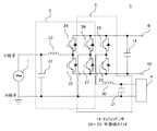
図14はこの実施の形態2における系統連系用電力変換システムにおいて、電力変換器に交流系統電源と電機負荷とが接続された部分を取り出して示す回路図であり、図1に示した実施の形態1と対応もしくは相当する構成部分には同一の符号を付す。
FIG. 14 is a circuit diagram showing a portion where the AC system power supply and the electrical load are connected to the power converter in the grid interconnection power conversion system according to the second embodiment. Constituent elements corresponding to or corresponding to the first embodiment are denoted by the same reference numerals.
この実施の形態2の系統連系用電力変換システムは、電力変換器5を構成するAC/DCコンバータ6の交流側に交流系統電源1が、直流側にはDC/ACインバータ8および電圧平滑用のリンクコンデンサ14がそれぞれ接続され、またDC/ACインバータ8の交流側には電機負荷4が接続される。
In the grid interconnection power conversion system of the second embodiment, the AC
さらに、AC/DCコンバータ6の直流側においてリンクコンデンサ14を介して接続された直流端子41、42には、図示していないが、第1のDC/DCコンバータ7を介して発電用直流電源2が、また第2のDC/DCコンバータ9を介して充放電用直流電源3がそれぞれ接続される。したがって、リンクコンデンサ14と直流端子41、42とが実施の形態1(図1)の直流リンク部10に対応している。
Furthermore, although not shown,
ここに、交流系統電源1は国内の単相2線式であり、この単相2線式は日本における100V系に相当し、交流系統電源1と電力変換器5が接続された状態では、接続する電機負荷4のN母線(接地母線)側は交流系統電源1の接地端子と同電位であることが前提である。
Here, the AC
上記のAC/DCコンバータ6は、4つの半導体スイッチ素子24、25、26、27を用いたフルブリッジ回路で構成されている。また、このAC/DCコンバータ6は、その交流側にフィルタコンデンサ22とフィルタリアクトル23とからからなる入力フィルタ部が設けられている。なお、フィルタコンデンサ22はRCフィルタで構成してもよい。また、フィルタコンデンサ22に並列にRCフィルタを追加してもよい。フィルタリアクトル23は、交流系統電流の力率を1に制御するためのリアクトルとしても利用する。
The AC /
一方、DC/ACインバータ8は、4つの半導体スイッチ素子26、27、28、29を用いたフルブリッジ回路で構成されている。この場合、上下2つの半導体スイッチ素子26、27は、AC/DCコンバータ6とDC/ACインバータ8とで共用する。また、このDC/ACインバータ8は、その交流側にフィルタリアクトル30とフィルタコンデンサ31とからなる出力フィルタ部を有している。
On the other hand, the DC /
なお、AC/DCコンバータ6とDC/ACインバータ8を構成する各半導体スイッチ素子24〜29は、図14ではIGBTを示しているが、これに限らず、例えばMOSFET、GTO、サイリスタで構成してもよい。
In addition, although each semiconductor switch element 24-29 which comprises the AC /
そして、上記AC/DCコンバータ6とDC/ACインバータ8で共通化された1アームを構成する2つの半導体スイッチ素子26、27間の接続点が電機負荷4のN母線(接地母線)側の端子に接続されている。また、DC/ACインバータ8の1アームを構成する2つの半導体スイッチ素子28、29間の接続点が電機負荷4のP母線(電源母線)側の端子に接続されている。
The connection point between the two
次に、AC/DCコンバータ6とDC/ACインバータ8とを同時に駆動する場合の、AC/DCコンバータ6の動作について、図15を用いて説明する。
Next, the operation of the AC /
交流系統電源1が正の期間では、共通化された1アームを構成する2つの半導体スイッチ素子26、27の内、下側の半導体スイッチ素子27をON、上側の半導体スイッチ素子26をOFFにし、他方の1アームを構成する両半導体スイッチ素子24、25をPWM制御することで、フィルタリアクトル23の励磁期間を調整してリンクコンデンサ14の電圧値を一定に保ち、かつ系統交流電流の力率を1に制御する。
During the period when the AC
一方、交流系統電源1が負の期間では、共通化された1アームを構成する2つの半導体スイッチ素子26、27の内、上側の半導体スイッチ素子26をON、下側の半導体スイッチ素子27をOFFにし、他方の1アームを構成する両半導体スイッチ素子24、25をPWM制御することで、上記と同様にフィルタリアクトル23の励磁期間を調整してリンクコンデンサ14の電圧値を一定に保ち、かつ系統交流電流の力率を1に制御する。これにより、リンクコンデンサ14から直流端子41、42に直流電力が供給される。なお、リンクコンデンサ14から交流系統電源1へ電力を回生する場合も同様である。
On the other hand, during the period when the AC
次に、AC/DCコンバータ6とDC/ACインバータ8を同時に駆動する場合の、DC/ACインバータ8の動作について図15を用いて説明する。
Next, the operation of the DC /
交流系統電源1が正の期間では、前述のように半導体スイッチ素子27をON、半導体スイッチ素子26をOFFにし、他方の1アームを構成する両半導体スイッチ素子28、29をPWM制御することで、交流系統電源1と同期した任意の正の正弦波の電圧を出力する。
一方、交流系統電源1が負の期間では、上記の通り半導体スイッチ素子26をON、半導体スイッチ素子27をOFFにし、他方の1アームを構成する両半導体スイッチ素子28、29をPWM制御することで、交流系統電源1と同期した任意の負の正弦波の電圧を出力する。これにより、フィルタリアクトル30とフィルタコンデンサ31とからなる出力フィルタを介して電機負荷4に交流電力が供給される。
During the period when the AC
On the other hand, when the AC
なお、AC/DCコンバータ6とDC/ACインバータ8を同時に駆動しない場合には、AC/DCコンバータ6単体にて全ての半導体スイッチ素子24〜27を同時にPWM制御してもよい。また、DC/ACインバータ8単体にて全ての半導体スイッチ素子26〜29を同時にPWM制御してもよい。
When the AC /
上記の説明は電機負荷4が交流負荷の場合であるが、直流の電機負荷11の場合には、リンクコンデンサ14を直流電源として利用する。すなわち、DC/ACインバータ8により、リンクコンデンサ14の直流電圧を降圧して、直流の電機負荷11へ電力供給する。この直流電圧を電機負荷11へ供給する場合の動作原理を次に説明する。なお、ここでは車が交流系統電源1に接続されず、AC/DCコンバータ6とDC/ACインバータ8とが同時に駆動されないこと、また、半導体スイッチ素子26〜29がすべてDC/ACインバータ8で使用できることを前提とする。
The above description is for the case where the
DC/ACインバータ8は、一方の1アームを構成する下側の半導体スイッチ素子27がON、上側の半導体スイッチ素子26がOFFされる。これにより、電機負荷11のN母線側はリンクコンデンサ14のマイナス電位に固定される。他方の1アームを構成する両半導体スイッチ素子28、29はPWM制御を行い、出力フィルタのフィルタリアクトル30へのリンクコンデンサ14からの電圧印加期間を調整する。すなわち、リンクコンデンサ14の直流電圧を降圧して、電機負荷11へ直流電圧を供給する。
In the DC /
上記のように半導体スイッチ素子28、29のON/OFFに伴う電力フローを図16、図17に示す。半導体スイッチ素子28がONし、かつ半導体スイッチ素子29がOFFした場合には、図16に示すように、リンクコンデンサ14の直流電圧がフィルタリアクトル30に印加され、電機負荷11へ直流電力が供給される。一方、半導体スイッチ素子29がONし、かつ半導体スイッチ素子28がOFFした場合には、図17に示すように、リンクコンデンサ14の直流電力は電機負荷11へは供給されず、半導体スイッチ素子27、29とフィルタリアクトル30を経由して電流が環流する。
The electric power flow accompanying ON / OFF of the
この実施の形態2では、フルブリッジ回路で構成されたAC/DCコンバータ6とDC/ACインバータ8について、上下の半導体スイッチ素子26、27で構成される1アームをAC/DCコンバータ6とDC/ACインバータ8とで共有することで、半導体スイッチ素子の個数削減による変換器サイズの低減が実現できる。また、交流系統電源1と電機負荷4、11のN端子が共通に接地されているため、国内単相2線式の接地要件を満たす。さらに、交流の電機負荷4に交流電力を供給できるだけでなく、直流の電機負荷11にも直流電圧を供給することができる。
In the second embodiment, with respect to the AC /
実施の形態3.
図18はこの実施の形態3における系統連系用電力変換システムにおいて、電力変換器に交流系統電源と電機負荷とが接続された部分を取り出して示す回路図であり、図14に示した実施の形態2と対応もしくは相当する構成部分には同一の符号を付す。
FIG. 18 is a circuit diagram showing a portion where the AC system power supply and the electrical load are connected to the power converter in the grid interconnection power conversion system according to the third embodiment. Constituent elements corresponding to or corresponding to the second embodiment are denoted by the same reference numerals.
上記の実施の形態2では、交流系統電源1を国内の単相2線式とした場合の、電力変換器5におけるAC/DCコンバータ6とDC/ACインバータ8の回路構成について説明したが、この実施の形態3では、交流系統電源1を国内の単相3線式とした場合のAC/DCコンバータ6と、DC/ACインバータ8の回路構成について説明する。なお、この場合の電機負荷4は交流負荷であり、また交流系統電源1は国内の単相3線式であるので、交流系統電源の中性点が接地されていることを前提としている。
In the second embodiment, the circuit configuration of the AC /
AC/DCコンバータ6は、フィルタコンデンサ22とフィルタリアクトル23とからなる入力フィルタ部、および4つの半導体スイッチ素子24、25、26、27からなるフルブリッジ回路で構成されている。なお、実施の形態2と同様、フィルタコンデンサ22はRCフィルタで構成してもよい。また、フィルタコンデンサ22に並列にRCフィルタを追加してもよい。フィルタリアクトル23は、交流系統電流の力率を1に制御するためのリアクトルとしても利用する。
The AC /
一方、DC/ACインバータ8は、上下2つの半導体スイッチ素子28、29によりハーフブリッジ回路が構成されるとともに、2つのコンデンサ14a、14bを直列接続してなるリンクコンデンサ14、およびフィルタリアクトル30とフィルタコンデンサ31とからなる出力フィルタ部を備えている。
On the other hand, in the DC /
そして、上下2つの半導体スイッチ素子28、29間の接続点はフィルタリアクトル30に接続され、交流の電機負荷4のN母線側は常に接地端子に接続される。また、リンクコンデンサ14は2つのコンデンサ14a、14bを直列接続した構成であり、上下のコンデンサ14a、14b間の中性点32が接地端子に接続される。
The connection point between the upper and lower
ここで、AC/DCコンバータ6は、実施の形態2と同様に、半導体スイッチ素子24〜27をPWM制御することで、リンクコンデンサ14の電圧値を一定に、かつ系統交流電流の力率を1に制御する。これにより、リンクコンデンサ14から直流端子41、42に直流電圧が供給される。リンクコンデンサ14から交流系統電源1へ電力を回生する場合も同様である。
Here, as in the second embodiment, the AC /
また、DC/ACインバータ8については、半導体スイッチ素子28がON、半導体スイッチ素子29がOFFとなると、リンクコンデンサ14の中性点32を基準としてプラスの電圧がフィルタリアクトル30とフィルタコンデンサ31に印加され、これとは逆に、半導体スイッチ素子29がON、半導体スイッチ素子28がOFFとなると、リンクコンデンサ14の中性点32を基準としてマイナスの電圧がフィルタリアクトル30とフィルタコンデンサ31に印加される。そして、上記両半導体スイッチ素子28、29の繰り返し動作により、電機負荷4へは交流電圧が印加される。
As for the DC /
上記の説明は電機負荷11が交流負荷の場合であるが、直流の電機負荷11に対して直流電力を供給する場合には、図19に示す構成が採用される。
すなわち、電機負荷11のN母線側の端子とリンクコンデンサ14の中性点32が共に接地されるとともに、電機負荷11のP母線側の端子とハーフブリッジ回路を構成する2つの半導体スイッチ素子28、29間の接続点とが接続されている。さらに、リンクコンデンサ14の中性点32と上記2つの半導体スイッチ素子28、29間の接続点との間がチョッパ駆動用の半導体スイッチ素子33(特許請求の範囲のスイッチに相当)を介して接続されている。なお、このチョッパ駆動用の半導体スイッチ素子33について、図19ではIGBTで示しているが、MOSFET、サイリスタ、GTOなどで構成してもよい。
その他の構成は図18に示した構成と同じであるので、詳しい説明は省略する。
The above description is for the case where the
That is, the N bus side terminal of the
The other configuration is the same as the configuration shown in FIG.
次に、図19の回路構成において、電機負荷11へ直流電圧を供給する場合の運転動作について説明する。
Next, the operation when the DC voltage is supplied to the
電機負荷11が直流負荷の場合には、リンクコンデンサ14のP端子側のコンデンサ14aを直流電圧源として利用する。そして、半導体スイッチ素子28、チョッパ駆動用の半導体スイッチ素子33、およびフィルタリアクトル30によって降圧チョッパの回路構成をとり、半導体スイッチ素子28のONデューティを調整することで、電機負荷11へ供給する直流電圧を調整する。この場合、半導体スイッチ素子29はOFFに保たれる。また、チョッパ駆動用の半導体スイッチ素子33はチョッパ回路の環流ダイオードとしての作用をする。
When the
すなわち、半導体スイッチ素子28がONした場合にはチョッパ駆動用の半導体スイッチ素子33はOFFとなり、コンデンサ14aの直流電圧がフィルタリアクトル30に印加されて電機負荷11へ直流電力が供給される。一方、半導体スイッチ素子28がOFFした場合にはチョッパ駆動用の半導体スイッチ素子33はONとなり、コンデンサ14aの直流電圧はフィルタリアクトル30に印加されず、チョッパ駆動用の半導体スイッチ素子33とフィルタリアクトル30を経由して電流が環流する。
That is, when the
この実施の形態3では、交流系統電源1が国内単相3線式の場合でも、交流系統電源1の接地端子と電機負荷4のN母線側の端子とを共通にして動作させることができる。また、チョッパ駆動用の半導体スイッチ素子33を設けることで、電機負荷が直流の電機負荷11の場合でも電力を供給することができる。
In the third embodiment, even when the AC
実施の形態4.
図20はこの実施の形態4における系統連系用電力変換システムにおいて、電力変換器に交流系統電源と電機負荷とが接続された部分を取り出して示す回路図であり、図18に示した実施の形態3と対応もしくは相当する構成部分には同一の符号を付す。
FIG. 20 is a circuit diagram showing a portion where the AC system power supply and the electrical load are connected to the power converter in the grid interconnection power conversion system according to the fourth embodiment, which is the embodiment shown in FIG. Constituent parts corresponding to or corresponding to the third embodiment are denoted by the same reference numerals.
上記の実施の形態2では交流系統電源1が単相2線式の場合に、また実施の形態3では交流系統電源1が単相3線式の場合に、それぞれ対応した電力変換器の構成について説明したが、この実施の形態4における電力変換器は、交流系統電源1として単相2線式と単相3線式のどちらが接続されても対応できるようにしたものである。
In the second embodiment, when the AC
すなわち、この実施の形態4の特徴は、AC/DCコンバータ6の交流側には必要に応じて単相2線式あるいは単相3線式の交流系統電源1が接続される。また、2つのコンデンサ14a、14bを直列接続したリンクコンデンサ14の中性点32と接地端子との間には中性点切替スイッチ34が設けられている。さらに、制御回路15には、図21に示すように、交流系統電源1の電圧実効値を演算して基準電圧と比較し、単相2線式と単相3線式の判定を行って上記中性点切替スイッチ34を動作させるための交流系統電源判定器35が設けられている。
その他の構成は図18に示した実施の形態3の場合と同様であるから、ここでは詳しい説明は省略する。
That is, the feature of the fourth embodiment is that a single-phase two-wire or single-phase three-wire
Since the other configuration is the same as that of the third embodiment shown in FIG. 18, detailed description is omitted here.
次に、交流系統電源1が単相2線式の場合と単相3線式の場合に対応した中性点切替スイッチ34の切替制御について説明する。
Next, switching control of the neutral
国内の単相2線式は100V系、単相3線式は200V系であるので、この実施の形態4では、基準電圧を100[Vrms]と200[Vrms]からマージン30[Vrms]をみた130[Vrms]〜170[Vrms]の間に定める。 Since the single-phase two-wire system in Japan is a 100V system and the single-phase three-wire system is a 200V system, in this fourth embodiment, a margin of 30 [Vrms] is seen from the reference voltage of 100 [Vrms] and 200 [Vrms]. It is determined between 130 [Vrms] and 170 [Vrms].
そして、交流系統電源1の電圧実効値の演算結果が130[Vrms]以下であれば、交流系統電源判定器35の出力が“0”となるので、この場合は国内単相2線式と判定して、中性点切替スイッチ34をOFFとする。これに対して、交流系統電源1の電圧実効値の演算結果が170[Vrms]以上であれば、交流系統電源判定器35の出力が“1”となるので、この場合は国内単相3線式と判定して、中性点切替スイッチ34をONとする。なお、基準電圧は、100[Vrms]と200[Vrms]が判定できる電圧値であれば、130[Vrms]〜170[Vrms]の範囲に限らずそれ以外であってもよい。
If the calculation result of the effective voltage value of the AC
上記交流系統電源判定器35により国内単相2線式と判定された結果、中性点切替スイッチがOFFとなった場合には、交流系統電源1のN母線側端子と電機負荷4のN母線側端子が共に接地される。この場合の回路構成は図14に示した実施の形態2における単相2線式の回路構成と同一であり、実施の形態2で説明したのと同様な運転動作を行う。
If the neutral point changeover switch is turned off as a result of the determination by the AC system power
また、交流系統電源判定器35により国内単相3線式と判定された結果、中性点切替スイッチがONとなった場合には、交流系統電源1の中性点と電機負荷4のN端子が共に接地される。この場合の回路構成は図18に示した実施の形態3における単相3線式の回路構成と同一であり、実施の形態3で説明したのと同様な運転動作を行う。
If the neutral point changeover switch is turned on as a result of the determination by the AC system power
なお、図20に示した構成に限らず、例えば図22に示すように、リンクコンデンサ14の中性点32とハーフブリッジ回路を構成する2つの半導体スイッチ28、29間の接続点との間をチョッパ駆動用の半導体スイッチ素子33で接続した構成としてもよい。
In addition to the configuration shown in FIG. 20, for example, as shown in FIG. 22, between the
そして、交流系統電源判定器35により交流系統電源1が単相2線式であると判定された場合、中性点切替スイッチ34がOFFとなり、かつ、チョッパ駆動用の半導体スイッチ素子33がOFFに保たれる。したがって、この場合には図14に示した構成に関して説明したのと同様な運転動作が行われる。
When the AC system power
また、交流系統電源判定器35により交流系統電源1が単相3線式であると判定された場合、中性点切替スイッチ34がONとなる。その際、交流の電機負荷4の場合、チョッパ駆動用の半導体スイッチ素子33はOFFに保たれる。したがって、この場合には図18に示した構成に関して説明したのと同様な運転動作が行われる。
When the AC system power
また、交流系統電源判定器35により交流系統電源1が単相3線式であると判定された場合、同様に中性点切替スイッチ34がONとなる。その際、直流の電機負荷11の場合、チョッパ駆動用の半導体スイッチ素子33はON/OFF駆動される。したがって、この場合には図19に示した構成に関して説明したのと同様な運転動作が行われる。
Further, when the AC system power
このように、この実施の形態4では、交流系統電源1が国内の単相3線式でも単相2線式のいずれでも、交流系統電源1の接地端子と電機負荷4のN母線側端子を共通にして動作させることができる。また、国内の単相3線式が接続される場合、図22に示したようにチョッパ駆動用の半導体スイッチ素子33を設けた構成とすることにより電機負荷4に直流電力を供給することができる。
Thus, in the fourth embodiment, the ground terminal of the AC
なお、この発明は、上記の実施の形態1〜4の各構成のみに限定されるものではなく、この発明の趣旨を逸脱しない範囲で各実施の形態1〜4について各種変形を加えたり、あるいは各実施の形態1〜4の構成を適宜に組み合わせることが可能である。 In addition, this invention is not limited only to each structure of said Embodiment 1-4, A various deformation | transformation is added about each Embodiment 1-4 in the range which does not deviate from the meaning of this invention, or It is possible to appropriately combine the configurations of the first to fourth embodiments.
1 交流系統電源、2 発電用直流電源、3 充放電用直流電源、
4 交流の電機負荷、5 電力変換器、6 AC/DCコンバータ、
7 第1のDC/DCコンバータ、8 DC/ACインバータ、
9 第2のDC/DCコンバータ、10 直流リンク部、11 直流の電機負荷、
12 第3のDC/DCコンバータ、14 リンクコンデンサ、15 制御回路、
24〜29 半導体スイッチ素子、32 リンクコンデンサの中性点、
33 チョッパ駆動用の半導体スイッチ素子(スイッチ)、34 中性点切替スイッチ。
1 AC power supply, 2 DC power supply for power generation, 3 DC power supply for charging / discharging,
4 AC electrical load, 5 power converter, 6 AC / DC converter,
7 first DC / DC converter, 8 DC / AC inverter,
9 Second DC / DC converter, 10 DC link unit, 11 DC electric load,
12 third DC / DC converter, 14 link capacitor, 15 control circuit,
24-29 semiconductor switch elements, 32 neutral points of link capacitors,
33 Semiconductor switch element (switch) for chopper drive, 34 Neutral point changeover switch.
Claims (15)
上記電力変換器は、直流母線相互間を接続する直流リンク部と、交流系統電源と上記直流リンク部の間を接続するAC/DCコンバータと、電機負荷と上記直流リンク部の間を接続するDC/ACインバータとを備え、上記AC/DCコンバータと上記DC/ACインバータを共に4つの半導体スイッチ素子からなるフルブリッジ回路で構成とするとともに、上記AC/DCコンバータと上記DC/ACインバータの1アームを共通化し、この共通化した1アームを構成する2つの半導体スイッチ素子間の接続点を上記電機負荷のN母線側の端子に接続しており、上記DC/ACインバータの上記共通化した1アームを構成する2つの半導体スイッチ素子の内、N母線側の半導体スイッチ素子をONに固定するとともに、他方の1アームを構成する2つの半導体スイッチ素子をスイッチングして上記電機負荷へ直流電圧を供給するものであり、
上記電力変換器の上記第1の接続部には上記交流系統電源が、上記第2の接続部には発電のみを行う発電用直流電源が、上記第3の接続部には充放電可能な充放電用直流電源が、上記第4の接続部には上記電機負荷がそれぞれ接続された状態において、上記交流系統電源と上記発電用直流電源を主電源として上記電機負荷へ電力を供給する場合に、上記発電用直流電源の発電電力を最大値に固定し、上記発電用直流電源の発電電力が上記電機負荷が必要な電力より少ない場合には、その不足電力を上記充放電用直流電源よりも上記交流系統電源を優先して上記電機負荷へ供給する一方、上記発電用直流電源の発電電力が上記電機負荷が必要な電力よりも多い場合には、その余剰電力により上記充放電用直流電源を充電する、ことを特徴とする系統連系用電力変換システム。 Comprising a power converter provided with first to fourth connecting portions;
The power converter includes a DC link unit that connects DC buses, an AC / DC converter that connects an AC system power source and the DC link unit, and a DC that connects an electric load and the DC link unit. An AC / DC inverter, and the AC / DC converter and the DC / AC inverter are both constituted by a full bridge circuit composed of four semiconductor switch elements, and one arm of the AC / DC converter and the DC / AC inverter. Is connected to the terminal on the N bus side of the electrical load, and the common one arm of the DC / AC inverter is connected to the connection point between the two semiconductor switch elements constituting the common one arm. Of the two semiconductor switch elements constituting the N bus, the semiconductor switch element on the N bus side is fixed to ON and the other one arm is configured. The two semiconductor switching elements to be switched is intended to supply a DC voltage to the electrical load,
The aforementioned first connecting portion of the power converter the AC system power source, the second power generating DC power source connection section that generates power only, the aforementioned third connecting portion rechargeable charge when a DC discharge source is above the fourth connection portion for supplying in a state where the electric load is connected respectively, the power the AC system power source and a DC power source for the power generation to the electric load as a main power source, When the generated power of the DC power source for power generation is fixed to the maximum value and the generated power of the DC power source for power generation is less than the power required for the electrical load, the shortage power is more than the DC power source for charge / discharge. While giving priority to the AC grid power supply to the electrical load, if the generated power of the DC power supply for power generation is higher than the power required for the electrical load, the surplus power is used to charge the DC power supply for charging / discharging. you, and wherein a call Mitsururen power conversion system for the system.
上記電力変換器は、直流母線相互間を接続する直流リンク部と、交流系統電源と上記直流リンク部の間を接続するAC/DCコンバータと、電機負荷と上記直流リンク部の間を接続するDC/ACインバータとを備え、上記AC/DCコンバータと上記DC/ACインバータを共に4つの半導体スイッチ素子からなるフルブリッジ回路で構成とするとともに、上記AC/DCコンバータと上記DC/ACインバータの1アームを共通化し、この共通化した1アームを構成する2つの半導体スイッチ素子間の接続点を上記電機負荷のN母線側の端子に接続しており、上記DC/ACインバータの上記共通化した1アームを構成する2つの半導体スイッチ素子の内、N母線側の半導体スイッチ素子をONに固定するとともに、他方の1アームを構成する2つの半導体スイッチ素子をスイッチングして上記電機負荷へ直流電圧を供給するものであり、
上記電力変換器の上記第1の接続部には上記交流系統電源が接続されず、上記第2の接続部には発電のみを行う発電用直流電源が、上記第3の接続部には充放電可能な充放電用直流電源が、上記第4の接続部には上記電機負荷がそれぞれ接続された状態において、上記発電用直流電源を主電源として上記電機負荷に電力を供給する場合に、上記発電用直流電源の発電電力を最大値に固定し、上記発電用直流電源の発電電力が上記電機負荷が必要とする電力量より多い場合には、その余剰電力により上記充放電用直流電源を充電し、上記充放電用直流電源が満充電に達したならば上記発電用直流電源の発電電力を上記電機負荷が必要とする電力まで減少させる、ことを特徴とする系統連系用電力変換システム。 Comprising a power converter provided with first to fourth connecting portions;
The power converter includes a DC link unit that connects DC buses, an AC / DC converter that connects an AC system power source and the DC link unit, and a DC that connects an electric load and the DC link unit. An AC / DC inverter, and the AC / DC converter and the DC / AC inverter are both constituted by a full bridge circuit composed of four semiconductor switch elements, and one arm of the AC / DC converter and the DC / AC inverter. Is connected to the terminal on the N bus side of the electrical load, and the common one arm of the DC / AC inverter is connected to the connection point between the two semiconductor switch elements constituting the common one arm. Of the two semiconductor switch elements constituting the N bus, the semiconductor switch element on the N bus side is fixed to ON and the other one arm is configured. The two semiconductor switching elements to be switched is intended to supply a DC voltage to the electrical load,
To the first connection portion of the power converter is not the AC system power source is connected, the second power generating DC power source connection section that generates power only, the aforementioned third connecting portion discharge discharge DC power supply capable of, in a state where the electric load is connected respectively to the fourth connection portion, when supplying power to the electric load DC power for the generator as a main power source, the generator When the generated power of the DC power supply for electric power is fixed to the maximum value and the generated power of the DC power supply for power generation is greater than the amount of power required by the electrical load, the DC power supply for charging and discharging is charged with the surplus power. the charging if discharging DC power supply has reached a fully charged Ru reduce the generated power of the power generating DC power supply to the power required by the above electric load, this and the power conversion system for system interconnection, characterized in .
上記電力変換器は、直流母線相互間を接続する直流リンク部と、交流系統電源と上記直流リンク部の間を接続するAC/DCコンバータと、電機負荷と上記直流リンク部の間を接続するDC/ACインバータとを備え、上記AC/DCコンバータと上記DC/ACインバータを共に4つの半導体スイッチ素子からなるフルブリッジ回路で構成とするとともに、上記AC/DCコンバータと上記DC/ACインバータの1アームを共通化し、この共通化した1アームを構成する2つの半導体スイッチ素子間の接続点を上記電機負荷のN母線側の端子に接続しており、上記DC/ACインバータの上記共通化した1アームを構成する2つの半導体スイッチ素子の内、N母線側の半導体スイッチ素子をONに固定するとともに、他方の1アームを構成する2つの半導体スイッチ素子をスイッチングして上記電機負荷へ直流電圧を供給するものであり、
上記電力変換器の上記第1の接続部には上記交流系統電源が、上記第2の接続部には発電のみを行う発電用直流電源が、上記第3の接続部には充放電可能な充放電用直流電源が、上記第4の接続部には上記電機負荷がそれぞれ接続された状態において、上記発電用直流電源を主電源として上記電機負荷と上記充放電用直流電源とを共に負荷と見なして電力供給を行う場合に、上記発電用直流電源の発電電力を最大値に、上記充放電用直流電源を所定の充電電力値にそれぞれ固定し、上記発電用直流電源の発電電力が上記電機負荷と上記充放電用直流電源への必要電力の総和より少ない場合には、その不足電力を上記交流系統電源から供給する一方、上記発電用直流電源の発電電力が上記電機負荷と上記充放電用直流電源への必要電力の総和よりも多い場合には、その余剰電力を上記交流系統電源に回生する、ことを特徴とする系統連系用電力変換システム。 Comprising a power converter provided with first to fourth connecting portions;
The power converter includes a DC link unit that connects DC buses, an AC / DC converter that connects an AC system power source and the DC link unit, and a DC that connects an electric load and the DC link unit. An AC / DC inverter, and the AC / DC converter and the DC / AC inverter are both constituted by a full bridge circuit composed of four semiconductor switch elements, and one arm of the AC / DC converter and the DC / AC inverter. Is connected to the terminal on the N bus side of the electrical load, and the common one arm of the DC / AC inverter is connected to the connection point between the two semiconductor switch elements constituting the common one arm. Of the two semiconductor switch elements constituting the N bus, the semiconductor switch element on the N bus side is fixed to ON and the other one arm is configured. The two semiconductor switching elements to be switched is intended to supply a DC voltage to the electrical load,
The aforementioned first connecting portion of the power converter the AC system power source, the second power generating DC power source connection section that generates power only, the aforementioned third connecting portion rechargeable charge regarded DC discharge source is above the fourth connection portion in a state where the electric load is connected respectively, the DC power supply the power and the electric load and the charging and discharging DC power supply and together load as the main power source When the power supply is performed, the generated power of the DC power supply for power generation is fixed to the maximum value, the DC power supply for charging / discharging is fixed to a predetermined charge power value, and the generated power of the DC power supply for power generation is And the charging / discharging DC power supply is less than the total power required for the charging / discharging DC power supply, the shortage power is supplied from the AC power supply, while the generated power of the generating DC power supply is the electrical load and the charging / discharging DC power supply. Total power required for power supply Even if large, the excess power you regenerated to the AC system power source, the grid interconnection power conversion system for system characterized by and this.
上記電力変換器は、直流母線相互間を接続する直流リンク部と、交流系統電源と上記直流リンク部の間を接続するAC/DCコンバータと、電機負荷と上記直流リンク部の間を接続するDC/ACインバータとを備え、上記AC/DCコンバータと上記DC/ACインバータを共に4つの半導体スイッチ素子からなるフルブリッジ回路で構成とするとともに、上記AC/DCコンバータと上記DC/ACインバータの1アームを共通化し、この共通化した1アームを構成する2つの半導体スイッチ素子間の接続点を上記電機負荷のN母線側の端子に接続しており、上記DC/ACインバータの上記共通化した1アームを構成する2つの半導体スイッチ素子の内、N母線側の半導体スイッチ素子をONに固定するとともに、他方の1アームを構成する2つの半導体スイッチ素子をスイッチングして上記電機負荷へ直流電圧を供給するものであり、
上記電力変換器の上記第1の接続部には上記交流系統電源が、上記第2の接続部には発電のみを行う発電用直流電源が、上記第3の接続部には充放電可能な充放電用直流電源が、上記第4の接続部には上記電機負荷がそれぞれ接続された状態において、上記発電用直流電源を主電源として上記電機負荷と上記交流系統電源を共に負荷と見なして電力供給を行う場合に、上記充放電用直流電源の充電量が満充電でない場合において、上記発電用直流電源の発電電力を最大値に固定し、上記発電用直流電源の発電電力が上記電機負荷の必要電力と上記交流系統電源の回生電力の総和より少ない場合には、上記交流系統電源のみで電力不足分だけ電力回生量を減少させる一方、上記発電用直流電源の発電電力が上記電機負荷の必要電力と上記交流系統電源の回生電力の総和より多い場合には、上記電機負荷の必要電力と上記充放電用直流電源の必要充電量の総和と上記発電用直流電源の発電電力との差電力を上記交流系統電源へ回生する、ことを特徴とする系統連系用電力変換システム。 Comprising a power converter provided with first to fourth connecting portions;
The power converter includes a DC link unit that connects DC buses, an AC / DC converter that connects an AC system power source and the DC link unit, and a DC that connects an electric load and the DC link unit. An AC / DC inverter, and the AC / DC converter and the DC / AC inverter are both constituted by a full bridge circuit composed of four semiconductor switch elements, and one arm of the AC / DC converter and the DC / AC inverter. Is connected to the terminal on the N bus side of the electrical load, and the common one arm of the DC / AC inverter is connected to the connection point between the two semiconductor switch elements constituting the common one arm. Of the two semiconductor switch elements constituting the N bus, the semiconductor switch element on the N bus side is fixed to ON and the other one arm is configured. The two semiconductor switching elements to be switched is intended to supply a DC voltage to the electrical load,
The aforementioned first connecting portion of the power converter the AC system power source, the second power generating DC power source connection section that generates power only, the aforementioned third connecting portion rechargeable charge DC discharge source is above the fourth connection portion in a state where the electric load is connected respectively, the power supply DC power for the power generation is regarded as the electric load and the AC system power source together load as the main power source When the charge amount of the charging / discharging DC power source is not fully charged, the generated power of the generating DC power source is fixed at the maximum value, and the generated power of the generating DC power source is necessary for the electric load. If the sum of the power and the regenerative power of the AC system power source is less than the sum of the AC system power source, the power regeneration amount is reduced by the shortage of power only by the AC system power source, while the generated power of the DC power source for power generation is the required power of the electrical load. And the above AC system If the sum of the regenerative power of the power source is greater than the sum of the regenerative power of the power source, the difference power between the sum of the required power of the electrical load and the required charge amount of the charge / discharge DC power source and the generated power of the DC power source for power generation It regenerative, power conversion system for system interconnection which is characterized and this.
上記電力変換器は、直流母線相互間を接続する直流リンク部と、交流系統電源と上記直流リンク部の間を接続するAC/DCコンバータと、電機負荷と上記直流リンク部の間を接続するDC/ACインバータとを備え、上記AC/DCコンバータを4つの半導体スイッチ素子からなるフルブリッジ回路で、上記DC/ACインバータを2つの半導体スイッチ素子からなるハーフブリッジ回路でそれぞれ構成し、また上記直流リンク部を2つのコンデンサを直列接続して構成するとともに、上記直流リンク部の両コンデンサの中性点を接地し、上記ハーフブリッジ回路を構成する2つの半導体スイッチ素子間の接続点を上記電機負荷のP母線側の端子に接続しており、
上記電力変換器の上記第1の接続部には上記交流系統電源が、上記第2の接続部には発電のみを行う発電用直流電源が、上記第3の接続部には充放電可能な充放電用直流電源が、上記第4の接続部には上記電機負荷がそれぞれ接続された状態において、上記交流系統電源と上記発電用直流電源を主電源として上記電機負荷へ電力を供給する場合に、上記発電用直流電源の発電電力を最大値に固定し、上記発電用直流電源の発電電力が上記電機負荷が必要な電力より少ない場合には、その不足電力を上記充放電用直流電源よりも上記交流系統電源を優先して上記電機負荷へ供給する一方、上記発電用直流電源の発電電力が上記電機負荷が必要な電力よりも多い場合には、その余剰電力により上記充放電用直流電源を充電する、ことを特徴とする系統連系用電力変換システム。 Comprising a power converter provided with first to fourth connecting portions;
The power converter includes a DC link unit that connects DC buses, an AC / DC converter that connects an AC system power source and the DC link unit, and a DC that connects an electric load and the DC link unit. A DC / AC inverter, wherein the AC / DC converter is a full-bridge circuit composed of four semiconductor switch elements, and the DC / AC inverter is a half-bridge circuit composed of two semiconductor switch elements. The section is constructed by connecting two capacitors in series, the neutral point of both capacitors of the DC link section is grounded, and the connection point between the two semiconductor switch elements constituting the half bridge circuit is connected to the electrical load. Connected to the terminal on the P bus side,
The aforementioned first connecting portion of the power converter the AC system power source, the second power generating DC power source connection section that generates power only, the aforementioned third connecting portion rechargeable charge when a DC discharge source is above the fourth connection portion for supplying in a state where the electric load is connected respectively, the power the AC system power source and a DC power source for the power generation to the electric load as a main power source, When the generated power of the DC power source for power generation is fixed to the maximum value and the generated power of the DC power source for power generation is less than the power required for the electrical load, the shortage power is more than the DC power source for charge / discharge. While giving priority to the AC grid power supply to the electrical load, if the generated power of the DC power supply for power generation is higher than the power required for the electrical load, the surplus power is used to charge the DC power supply for charging / discharging. you, and wherein a call Mitsururen power conversion system for the system.
上記電力変換器は、直流母線相互間を接続する直流リンク部と、交流系統電源と上記直流リンク部の間を接続するAC/DCコンバータと、電機負荷と上記直流リンク部の間を接続するDC/ACインバータとを備え、上記AC/DCコンバータを4つの半導体スイッチ素子からなるフルブリッジ回路で、上記DC/ACインバータを2つの半導体スイッチ素子からなるハーフブリッジ回路でそれぞれ構成し、また上記直流リンク部を2つのコンデンサを直列接続して構成するとともに、上記直流リンク部の両コンデンサの中性点を接地し、上記ハーフブリッジ回路を構成する2つの半導体スイッチ素子間の接続点を上記電機負荷のP母線側の端子に接続しており、
上記電力変換器の上記第1の接続部には上記交流系統電源が接続されず、上記第2の接続部には発電のみを行う発電用直流電源が、上記第3の接続部には充放電可能な充放電用直流電源が、上記第4の接続部には電機負荷がそれぞれ接続された状態において、上記発電用直流電源を主電源として上記電機負荷に電力を供給する場合に、上記発電用直流電源の発電電力を最大値に固定し、上記発電用直流電源の発電電力が上記電機負荷が必要とする電力量より多い場合には、その余剰電力により上記充放電用直流電源を充電し、上記充放電用直流電源が満充電に達したならば上記発電用直流電源の発電電力を上記電機負荷が必要とする電力まで減少させる、ことを特徴とする系統連系用電力変換システム。 Comprising a power converter provided with first to fourth connecting portions;
The power converter includes a DC link unit that connects DC buses, an AC / DC converter that connects an AC system power source and the DC link unit, and a DC that connects an electric load and the DC link unit. A DC / AC inverter, wherein the AC / DC converter is a full-bridge circuit composed of four semiconductor switch elements, and the DC / AC inverter is a half-bridge circuit composed of two semiconductor switch elements. The section is constructed by connecting two capacitors in series, the neutral point of both capacitors of the DC link section is grounded, and the connection point between the two semiconductor switch elements constituting the half bridge circuit is connected to the electrical load. Connected to the terminal on the P bus side,
To the first connection portion of the power converter is not the AC system power source is connected, the second power generating DC power source connection section that generates power only, the aforementioned third connecting portion discharge When a possible DC power supply for charging / discharging supplies power to the electrical load using the power generation DC power supply as a main power supply in a state where an electrical load is connected to the fourth connection portion, When the generated power of the DC power source is fixed to the maximum value and the generated power of the DC power source for power generation is larger than the amount of power required by the electrical load, the DC power source for charging / discharging is charged with the surplus power, the charge if discharging DC power supply has reached a fully charged Ru reduce the generated power of the power generating DC power supply to the power required by the above electric load, the grid interconnection power conversion system for system characterized by and this.
上記電力変換器は、直流母線相互間を接続する直流リンク部と、交流系統電源と上記直流リンク部の間を接続するAC/DCコンバータと、電機負荷と上記直流リンク部の間を接続するDC/ACインバータとを備え、上記AC/DCコンバータを4つの半導体スイッチ素子からなるフルブリッジ回路で、上記DC/ACインバータを2つの半導体スイッチ素子からなるハーフブリッジ回路でそれぞれ構成し、また上記直流リンク部を2つのコンデンサを直列接続して構成するとともに、上記直流リンク部の両コンデンサの中性点を接地し、上記ハーフブリッジ回路を構成する2つの半導体スイッチ素子間の接続点を上記電機負荷のP母線側の端子に接続しており、
上記電力変換器の上記第1の接続部には上記交流系統電源が、上記第2の接続部には発電のみを行う発電用直流電源が、上記第3の接続部には充放電可能な充放電用直流電源が、上記第4の接続部には上記電機負荷がそれぞれ接続された状態において、上記発電用直流電源を主電源として上記電機負荷と上記充放電用直流電源とを共に負荷と見なして電力供給を行う場合に、上記発電用直流電源の発電電力を最大値に、上記充放電用直流電源を所定の充電電力値にそれぞれ固定し、上記発電用直流電源の発電電力が上記電機負荷と上記充放電用直流電源への必要電力の総和より少ない場合には、その不足電力を上記交流系統電源から供給する一方、上記発電用直流電源の発電電力が上記電機負荷と上記充放電用直流電源への必要電力の総和よりも多い場合には、その余剰電力を上記交流系統電源に回生する、ことを特徴とする系統連系用電力変換システム。 Comprising a power converter provided with first to fourth connecting portions;
The power converter includes a DC link unit that connects DC buses, an AC / DC converter that connects an AC system power source and the DC link unit, and a DC that connects an electric load and the DC link unit. A DC / AC inverter, wherein the AC / DC converter is a full-bridge circuit composed of four semiconductor switch elements, and the DC / AC inverter is a half-bridge circuit composed of two semiconductor switch elements. The section is constructed by connecting two capacitors in series, the neutral point of both capacitors of the DC link section is grounded, and the connection point between the two semiconductor switch elements constituting the half bridge circuit is connected to the electrical load. Connected to the terminal on the P bus side,
The aforementioned first connecting portion of the power converter the AC system power source, the second power generating DC power source connection section that generates power only, the aforementioned third connecting portion rechargeable charge regarded DC discharge source is above the fourth connection portion in a state where the electric load is connected respectively, the DC power supply the power and the electric load and the charging and discharging DC power supply and together load as the main power source When the power supply is performed, the generated power of the DC power supply for power generation is fixed to the maximum value, the DC power supply for charging / discharging is fixed to a predetermined charge power value, and the generated power of the DC power supply for power generation is And the charging / discharging DC power supply is less than the total power required for the charging / discharging DC power supply, the shortage power is supplied from the AC power supply, while the generated power of the generating DC power supply is the electrical load and the charging / discharging DC power supply. Total power required for power supply Even if large, the excess power you regenerated to the AC system power source, the grid interconnection power conversion system for system characterized by and this.
上記電力変換器は、直流母線相互間を接続する直流リンク部と、交流系統電源と上記直流リンク部の間を接続するAC/DCコンバータと、電機負荷と上記直流リンク部の間を接続するDC/ACインバータとを備え、上記AC/DCコンバータを4つの半導体スイッチ素子からなるフルブリッジ回路で、上記DC/ACインバータを2つの半導体スイッチ素子からなるハーフブリッジ回路でそれぞれ構成し、また上記直流リンク部を2つのコンデンサを直列接続して構成するとともに、上記直流リンク部の両コンデンサの中性点を接地し、上記ハーフブリッジ回路を構成する2つの半導体スイッチ素子間の接続点を上記電機負荷のP母線側の端子に接続しており、
上記電力変換器の上記第1の接続部には上記交流系統電源が、上記第2の接続部には発電のみを行う発電用直流電源が、上記第3の接続部には充放電可能な充放電用直流電源が、上記第4の接続部には上記電機負荷がそれぞれ接続された状態において、上記発電用直流電源を主電源として上記電機負荷と上記交流系統電源を共に負荷と見なして電力供給を行う場合に、上記充放電用直流電源の充電量が満充電でない場合において、上記発電用直流電源の発電電力を最大値に固定し、上記発電用直流電源の発電電力が上記電機負荷の必要電力と上記交流系統電源の回生電力の総和より少ない場合には、上記交流系統電源のみで電力不足分だけ電力回生量を減少させる一方、上記発電用直流電源の発電電力が上記電機負荷の必要電力と上記交流系統電源の回生電力の総和より多い場合には、上記電機負荷の必要電力と上記充放電用直流電源の必要充電量の総和と上記発電用直流電源の発電電力との差電力を上記交流系統電源へ回生する、ことを特徴とする系統連系用電力変換システム。 Comprising a power converter provided with first to fourth connecting portions;
The power converter includes a DC link unit that connects DC buses, an AC / DC converter that connects an AC system power source and the DC link unit, and a DC that connects an electric load and the DC link unit. A DC / AC inverter, wherein the AC / DC converter is a full-bridge circuit composed of four semiconductor switch elements, and the DC / AC inverter is a half-bridge circuit composed of two semiconductor switch elements. The section is constructed by connecting two capacitors in series, the neutral point of both capacitors of the DC link section is grounded, and the connection point between the two semiconductor switch elements constituting the half bridge circuit is connected to the electrical load. Connected to the terminal on the P bus side,
The aforementioned first connecting portion of the power converter the AC system power source, the second power generating DC power source connection section that generates power only, the aforementioned third connecting portion rechargeable charge DC discharge source is above the fourth connection portion in a state where the electric load is connected respectively, the power supply DC power for the power generation is regarded as the electric load and the AC system power source together load as the main power source When the charge amount of the charging / discharging DC power source is not fully charged, the generated power of the generating DC power source is fixed at the maximum value, and the generated power of the generating DC power source is necessary for the electric load. If the sum of the power and the regenerative power of the AC system power source is less than the sum of the AC system power source, the power regeneration amount is reduced by the shortage of power only by the AC system power source, while the generated power of the DC power source for power generation is the required power of the electrical load. And the above AC system If the sum of the regenerative power of the power source is greater than the sum of the regenerative power of the power source, the difference power between the sum of the required power of the electrical load and the required charge amount of the charge / discharge DC power source and the generated power of the DC power source for power generation It regenerative, power conversion system for system interconnection which is characterized and this.
Priority Applications (1)
| Application Number | Priority Date | Filing Date | Title |
|---|---|---|---|
| JP2012006659A JP5843624B2 (en) | 2012-01-17 | 2012-01-17 | Power conversion system for grid connection |
Applications Claiming Priority (1)
| Application Number | Priority Date | Filing Date | Title |
|---|---|---|---|
| JP2012006659A JP5843624B2 (en) | 2012-01-17 | 2012-01-17 | Power conversion system for grid connection |
Publications (3)
| Publication Number | Publication Date |
|---|---|
| JP2013150369A JP2013150369A (en) | 2013-08-01 |
| JP2013150369A5 JP2013150369A5 (en) | 2013-11-21 |
| JP5843624B2 true JP5843624B2 (en) | 2016-01-13 |
Family
ID=49047385
Family Applications (1)
| Application Number | Title | Priority Date | Filing Date |
|---|---|---|---|
| JP2012006659A Expired - Fee Related JP5843624B2 (en) | 2012-01-17 | 2012-01-17 | Power conversion system for grid connection |
Country Status (1)
| Country | Link |
|---|---|
| JP (1) | JP5843624B2 (en) |
Families Citing this family (14)
| Publication number | Priority date | Publication date | Assignee | Title |
|---|---|---|---|---|
| JP2015139322A (en) * | 2014-01-23 | 2015-07-30 | 国立大学法人 東京大学 | power network system |
| JP6308014B2 (en) * | 2014-05-20 | 2018-04-11 | 株式会社Ihi | Power management system |
| JP2016005399A (en) * | 2014-06-18 | 2016-01-12 | 株式会社デンソー | Charging/discharging apparatus |
| WO2016017642A1 (en) * | 2014-07-30 | 2016-02-04 | 日本電気株式会社 | Control device, power-feeding system, control method, and program |
| CN105471069A (en) * | 2016-01-05 | 2016-04-06 | 海鹰航空通用装备有限责任公司 | Vehicle-mounted power supply management and control system and equipment for small-sized unmanned aerial vehicle |
| EP3444922B8 (en) | 2016-04-14 | 2021-03-17 | Toshiba Mitsubishi-Electric Industrial Systems Corporation | Uninterruptible power source device |
| CN107508471B (en) | 2016-06-14 | 2020-11-06 | 松下知识产权经营株式会社 | Power conversion circuit, power conversion device, power transmission device, power reception device, and power transmission system |
| JP6710281B2 (en) * | 2016-08-19 | 2020-06-17 | 三菱電機株式会社 | Power converter |
| WO2018078683A1 (en) * | 2016-10-24 | 2018-05-03 | 東芝三菱電機産業システム株式会社 | Power supply system |
| JP6813830B2 (en) * | 2016-12-26 | 2021-01-13 | 有限会社ワタナベエレクトロニクス | Power switching device |
| CN108075651A (en) * | 2017-12-13 | 2018-05-25 | 杭州富特科技股份有限公司 | Vehicle-mounted charging device and system |
| JP7088091B2 (en) * | 2019-03-14 | 2022-06-21 | オムロン株式会社 | Power supply system, power transmission device and portable power supply device |
| WO2021192108A1 (en) * | 2020-03-25 | 2021-09-30 | Tdk株式会社 | Power management device, power feeding system, and power management method |
| JP6851554B1 (en) * | 2020-04-20 | 2021-03-31 | 三菱電機株式会社 | Power converter and air conditioner |
Family Cites Families (11)
| Publication number | Priority date | Publication date | Assignee | Title |
|---|---|---|---|---|
| JPH04372537A (en) * | 1991-06-21 | 1992-12-25 | Sanyo Electric Co Ltd | Composite input station |
| JP2001095179A (en) * | 1999-09-17 | 2001-04-06 | Hitachi Ltd | Electricity storing system and electric power feeding system |
| JP2002354677A (en) * | 2001-05-28 | 2002-12-06 | Japan Storage Battery Co Ltd | Power conditioner for solar energy generation |
| JP2003032906A (en) * | 2001-07-11 | 2003-01-31 | Osaka Gas Co Ltd | Power supply unit |
| JP2003116224A (en) * | 2001-10-09 | 2003-04-18 | Canon Inc | Photovoltaic generation system, power converter thereof, and control method therefor |
| JP4140244B2 (en) * | 2002-01-31 | 2008-08-27 | 松下電器産業株式会社 | Inverter control method and power saving device using the control method |
| JP2007124864A (en) * | 2005-10-31 | 2007-05-17 | Sharp Corp | Power conversion system |
| JP2007166818A (en) * | 2005-12-15 | 2007-06-28 | Sharp Corp | Power supply system and control method thereof |
| JP2008306814A (en) * | 2007-06-06 | 2008-12-18 | Osaka Gas Co Ltd | Distributed power supply system |
| JP4781425B2 (en) * | 2008-12-25 | 2011-09-28 | 本田技研工業株式会社 | Power supply system between vehicle and house |
| JP5584763B2 (en) * | 2010-06-22 | 2014-09-03 | シャープ株式会社 | DC power distribution system |
-
2012
- 2012-01-17 JP JP2012006659A patent/JP5843624B2/en not_active Expired - Fee Related
Also Published As
| Publication number | Publication date |
|---|---|
| JP2013150369A (en) | 2013-08-01 |
Similar Documents
| Publication | Publication Date | Title |
|---|---|---|
| JP5843624B2 (en) | Power conversion system for grid connection | |
| Maroti et al. | The state-of-the-art of power electronics converters configurations in electric vehicle technologies | |
| Pires et al. | Power converter interfaces for electrochemical energy storage systems–A review | |
| CN109687722B (en) | Integrated multi-mode power converter for electric automobile and control method thereof | |
| CA2677847C (en) | Control system for hybrid vehicles with reconfigurable multi-function power converter | |
| US9000711B2 (en) | Power converter | |
| JP4538057B2 (en) | DC / DC converter device | |
| CN106476635A (en) | Hybrid system with multiple energy storing devices | |
| CN103171452A (en) | Dual-power supply management system and dual-power supply management method for electric vehicle | |
| US7605497B2 (en) | Two-source inverter | |
| CN104608649B (en) | Integrated electric energy of electric automobile transformation system | |
| JP2013150369A5 (en) | ||
| KR20120125886A (en) | integrated module of inverter and charger circuit | |
| Dorn-Gomba et al. | A novel hybrid energy storage system using the multi-source inverter | |
| JP5350843B2 (en) | Power supply control device and power supply control method | |
| JP2009027815A (en) | Grid-connected converter device | |
| D'Arco et al. | Power and balancing control considerations on modular multilevel converters for battery electric vehicles | |
| CN103730940A (en) | Vehicle-mounted charger of electric automobile | |
| CN101483388A (en) | Method of driving DC/DC converter, and DC/DC converter | |
| CN109367417A (en) | Two-stage bidirectional power inverter and control method with charging and V2G function | |
| CN103085676A (en) | Power generating system of extended-range electric vehicle | |
| CN209079670U (en) | Two-stage bidirectional power inverter with charging and V2G function | |
| Li et al. | An integrated electric vehicle power conversion system using modular multilevel converter | |
| JP6966871B2 (en) | Battery system | |
| CN108136931B (en) | Improved power supply device with multiple power sources |
Legal Events
| Date | Code | Title | Description |
|---|---|---|---|
| A521 | Written amendment |
Free format text: JAPANESE INTERMEDIATE CODE: A523 Effective date: 20131007 |
|
| A621 | Written request for application examination |
Free format text: JAPANESE INTERMEDIATE CODE: A621 Effective date: 20131007 |
|
| A977 | Report on retrieval |
Free format text: JAPANESE INTERMEDIATE CODE: A971007 Effective date: 20140623 |
|
| A131 | Notification of reasons for refusal |
Free format text: JAPANESE INTERMEDIATE CODE: A131 Effective date: 20140723 |
|
| A521 | Written amendment |
Free format text: JAPANESE INTERMEDIATE CODE: A523 Effective date: 20140904 |
|
| A131 | Notification of reasons for refusal |
Free format text: JAPANESE INTERMEDIATE CODE: A131 Effective date: 20150303 |
|
| A521 | Written amendment |
Free format text: JAPANESE INTERMEDIATE CODE: A523 Effective date: 20150417 |
|
| TRDD | Decision of grant or rejection written | ||
| A01 | Written decision to grant a patent or to grant a registration (utility model) |
Free format text: JAPANESE INTERMEDIATE CODE: A01 Effective date: 20151020 |
|
| A61 | First payment of annual fees (during grant procedure) |
Free format text: JAPANESE INTERMEDIATE CODE: A61 Effective date: 20151117 |
|
| R150 | Certificate of patent or registration of utility model |
Ref document number: 5843624 Country of ref document: JP Free format text: JAPANESE INTERMEDIATE CODE: R150 |
|
| R250 | Receipt of annual fees |
Free format text: JAPANESE INTERMEDIATE CODE: R250 |
|
| R250 | Receipt of annual fees |
Free format text: JAPANESE INTERMEDIATE CODE: R250 |
|
| LAPS | Cancellation because of no payment of annual fees |