JP5835765B2 - Elastic wave element - Google Patents
Elastic wave element Download PDFInfo
- Publication number
- JP5835765B2 JP5835765B2 JP2015524110A JP2015524110A JP5835765B2 JP 5835765 B2 JP5835765 B2 JP 5835765B2 JP 2015524110 A JP2015524110 A JP 2015524110A JP 2015524110 A JP2015524110 A JP 2015524110A JP 5835765 B2 JP5835765 B2 JP 5835765B2
- Authority
- JP
- Japan
- Prior art keywords
- axis
- electrode
- quartz substrate
- range
- vibration
- Prior art date
- Legal status (The legal status is an assumption and is not a legal conclusion. Google has not performed a legal analysis and makes no representation as to the accuracy of the status listed.)
- Active
Links
- 239000000758 substrate Substances 0.000 claims description 88
- 239000010453 quartz Substances 0.000 claims description 81
- VYPSYNLAJGMNEJ-UHFFFAOYSA-N silicon dioxide Inorganic materials O=[Si]=O VYPSYNLAJGMNEJ-UHFFFAOYSA-N 0.000 claims description 81
- 230000005284 excitation Effects 0.000 claims description 56
- 230000010355 oscillation Effects 0.000 claims description 33
- 239000013078 crystal Substances 0.000 claims description 27
- 238000001465 metallisation Methods 0.000 claims description 16
- 230000002159 abnormal effect Effects 0.000 claims description 9
- 238000011161 development Methods 0.000 claims description 2
- 239000010408 film Substances 0.000 description 30
- 230000008878 coupling Effects 0.000 description 12
- 238000010168 coupling process Methods 0.000 description 12
- 238000005859 coupling reaction Methods 0.000 description 12
- 239000010931 gold Substances 0.000 description 12
- 238000005530 etching Methods 0.000 description 11
- 238000000034 method Methods 0.000 description 10
- 239000006185 dispersion Substances 0.000 description 9
- 238000004519 manufacturing process Methods 0.000 description 8
- 239000010409 thin film Substances 0.000 description 6
- 235000019687 Lamb Nutrition 0.000 description 5
- 230000000694 effects Effects 0.000 description 5
- 230000001902 propagating effect Effects 0.000 description 5
- 210000000695 crystalline len Anatomy 0.000 description 4
- 230000003628 erosive effect Effects 0.000 description 4
- 230000001976 improved effect Effects 0.000 description 4
- 230000001965 increasing effect Effects 0.000 description 4
- 238000010897 surface acoustic wave method Methods 0.000 description 4
- 238000009826 distribution Methods 0.000 description 3
- 229910052737 gold Inorganic materials 0.000 description 3
- 239000000463 material Substances 0.000 description 3
- 238000009966 trimming Methods 0.000 description 3
- 238000001039 wet etching Methods 0.000 description 3
- 229910052782 aluminium Inorganic materials 0.000 description 2
- 238000004458 analytical method Methods 0.000 description 2
- 238000004364 calculation method Methods 0.000 description 2
- 238000004891 communication Methods 0.000 description 2
- 239000003989 dielectric material Substances 0.000 description 2
- 239000000835 fiber Substances 0.000 description 2
- PCHJSUWPFVWCPO-UHFFFAOYSA-N gold Chemical compound [Au] PCHJSUWPFVWCPO-UHFFFAOYSA-N 0.000 description 2
- 239000007769 metal material Substances 0.000 description 2
- 238000012545 processing Methods 0.000 description 2
- 230000001105 regulatory effect Effects 0.000 description 2
- 229910004298 SiO 2 Inorganic materials 0.000 description 1
- XAGFODPZIPBFFR-UHFFFAOYSA-N aluminium Chemical compound [Al] XAGFODPZIPBFFR-UHFFFAOYSA-N 0.000 description 1
- 229910052802 copper Inorganic materials 0.000 description 1
- 230000007423 decrease Effects 0.000 description 1
- 238000000151 deposition Methods 0.000 description 1
- 238000013461 design Methods 0.000 description 1
- 230000006866 deterioration Effects 0.000 description 1
- 238000010586 diagram Methods 0.000 description 1
- 230000005684 electric field Effects 0.000 description 1
- 230000002349 favourable effect Effects 0.000 description 1
- 230000001939 inductive effect Effects 0.000 description 1
- 238000005259 measurement Methods 0.000 description 1
- 239000002184 metal Substances 0.000 description 1
- 229910052751 metal Inorganic materials 0.000 description 1
- 230000003287 optical effect Effects 0.000 description 1
- 230000002093 peripheral effect Effects 0.000 description 1
- 229910052715 tantalum Inorganic materials 0.000 description 1
- 230000002123 temporal effect Effects 0.000 description 1
Images


Classifications
-
- H—ELECTRICITY
- H03—ELECTRONIC CIRCUITRY
- H03H—IMPEDANCE NETWORKS, e.g. RESONANT CIRCUITS; RESONATORS
- H03H9/00—Networks comprising electromechanical or electro-acoustic devices; Electromechanical resonators
- H03H9/02—Details
- H03H9/02535—Details of surface acoustic wave devices
- H03H9/02614—Treatment of substrates, e.g. curved, spherical, cylindrical substrates ensuring closed round-about circuits for the acoustical waves
- H03H9/02622—Treatment of substrates, e.g. curved, spherical, cylindrical substrates ensuring closed round-about circuits for the acoustical waves of the surface, including back surface
-
- H—ELECTRICITY
- H03—ELECTRONIC CIRCUITRY
- H03H—IMPEDANCE NETWORKS, e.g. RESONANT CIRCUITS; RESONATORS
- H03H9/00—Networks comprising electromechanical or electro-acoustic devices; Electromechanical resonators
- H03H9/02—Details
- H03H9/02228—Guided bulk acoustic wave devices or Lamb wave devices having interdigital transducers situated in parallel planes on either side of a piezoelectric layer
-
- H—ELECTRICITY
- H03—ELECTRONIC CIRCUITRY
- H03H—IMPEDANCE NETWORKS, e.g. RESONANT CIRCUITS; RESONATORS
- H03H9/00—Networks comprising electromechanical or electro-acoustic devices; Electromechanical resonators
- H03H9/02—Details
- H03H9/02535—Details of surface acoustic wave devices
- H03H9/02543—Characteristics of substrate, e.g. cutting angles
- H03H9/02551—Characteristics of substrate, e.g. cutting angles of quartz substrates
-
- H—ELECTRICITY
- H03—ELECTRONIC CIRCUITRY
- H03H—IMPEDANCE NETWORKS, e.g. RESONANT CIRCUITS; RESONATORS
- H03H9/00—Networks comprising electromechanical or electro-acoustic devices; Electromechanical resonators
- H03H9/02—Details
- H03H9/02535—Details of surface acoustic wave devices
- H03H9/02818—Means for compensation or elimination of undesirable effects
- H03H9/02834—Means for compensation or elimination of undesirable effects of temperature influence
-
- H—ELECTRICITY
- H03—ELECTRONIC CIRCUITRY
- H03H—IMPEDANCE NETWORKS, e.g. RESONANT CIRCUITS; RESONATORS
- H03H9/00—Networks comprising electromechanical or electro-acoustic devices; Electromechanical resonators
- H03H9/02—Details
- H03H9/125—Driving means, e.g. electrodes, coils
- H03H9/145—Driving means, e.g. electrodes, coils for networks using surface acoustic waves
-
- H—ELECTRICITY
- H03—ELECTRONIC CIRCUITRY
- H03H—IMPEDANCE NETWORKS, e.g. RESONANT CIRCUITS; RESONATORS
- H03H9/00—Networks comprising electromechanical or electro-acoustic devices; Electromechanical resonators
- H03H9/15—Constructional features of resonators consisting of piezoelectric or electrostrictive material
- H03H9/17—Constructional features of resonators consisting of piezoelectric or electrostrictive material having a single resonator
- H03H9/171—Constructional features of resonators consisting of piezoelectric or electrostrictive material having a single resonator implemented with thin-film techniques, i.e. of the film bulk acoustic resonator [FBAR] type
Description
本発明は、コンピュータや通信機器等における高周波発振源に用いられる弾性波素子に関するものである。 The present invention relates to an acoustic wave element used for a high-frequency oscillation source in a computer, a communication device or the like.
現在、各種の電子機器に搭載されている発振源としては、主にATカットの水晶振動子が多く用いられ、高周波で使用する場合はPLLによって所定の周波数に逓倍して使用している。また、高周波でノイズ等の少ない信号を必要とする場合は、弾性表面波を利用した共振子を直接発振源として使用する場合もある。 At present, as an oscillation source mounted on various electronic devices, an AT-cut crystal resonator is mainly used, and when used at a high frequency, it is multiplied to a predetermined frequency by a PLL. In addition, when a signal with high frequency and low noise is required, a resonator using a surface acoustic wave may be directly used as an oscillation source.
ATカットによる水晶振動子は、安定した周波数特性が得られることから、多くの電子機器の発振源として用いられているが、高速動作するコンピュータや通信機器などの高周波発振源として用いる場合は、厚みを薄くしたり、平坦度を上げたりするなどの高精度の加工技術が必要とされている。 An AT-cut quartz crystal unit is used as an oscillation source in many electronic devices because stable frequency characteristics can be obtained, but when used as a high-frequency oscillation source in computers or communication devices that operate at high speed, High-precision processing techniques are required, such as reducing the thickness and increasing the flatness.
一方、弾性表面波は、圧電基板の表層面に発生する縦波あるいは横波を利用したものであり、その周波数は速度に比例し、波長に反比例する特性を有している。この弾性表面波を用いたデバイスは、所定のカット角で形成された圧電基板の表面に複数の電極指を櫛形状に配置してなる励振電極を形成し、この励振電極の膜厚や各電極指のピッチを調整することによって、所定の発振周波数を得るようになっている。 On the other hand, the surface acoustic wave uses a longitudinal wave or a transverse wave generated on the surface of the piezoelectric substrate, and has a characteristic that the frequency is proportional to the speed and inversely proportional to the wavelength. In this device using surface acoustic waves, an excitation electrode is formed by arranging a plurality of electrode fingers in a comb shape on the surface of a piezoelectric substrate formed with a predetermined cut angle. A predetermined oscillation frequency is obtained by adjusting the pitch of the finger.
特許文献1に開示されている圧電デバイスは、回転Yカットの水晶基板に生じる弾性表面波の中のラム波モードを用いたものであり、水晶基板の表面に櫛形状の励振電極を有し、裏面に周波数調整用の薄膜を有した構造となっている。この圧電振動子は、温度特性が従来型のSTカット共振子と同じ2次温度特性を有している。
The piezoelectric device disclosed in
特許文献2,3には、ラム波を発振させるための振動子が開示されている。このラム波型の振動子は、3次温度特性が得られる点で、ATカットのような厚みすべり振動子よりも周波数特性の改善が図られている。しかしながら、水晶基板のカット角が2軸の回転角度によって規定されているものであることから、作製のしやすさや温度特性のばらつき等に課題がある。
また、特許文献4には、オイラー角表示で規定された回転Yカットの水晶基板を用いて構成された高周波振動子が開示されている。
Further,
なお、上記特許文献2乃至4に開示されている振動子は、圧電基板の表面に櫛形状の励振電極を配置した構造となっており、圧電基板の裏面には周波数を調整するための薄膜等は設けられていない。
The vibrators disclosed in
特許文献5には、励振電極におけるメタライゼーションレシオと、前記励振電極の膜厚との関係についての記載がある。
なお、上記特許文献5に開示されている振動子は、圧電基板の表面に励振電極を配置した構造となっており、圧電基板の裏面には周波数を調整するための薄膜等は設けられていない。
The vibrator disclosed in
特許文献6には、櫛形状の励振電極の裏面側から電極膜をトリミングすることによって周波数の調整を行う旨の記載がある。
また、特許文献7には、電極面に薄膜を設け、この薄膜をトリミングすることによって、周波数の調整を行う方法が開示されている。
上記ATカットによる水晶振動子にあっては、発振周波数の精度は高いが、所定の周波数に逓倍する際に、位相雑音や信号の時間的なズレや揺らぎなどによるジッタが発生するなどの問題がある。一方、弾性波素子では、高周波を直接発振することが可能であるため、位相雑音やジッタ特性は良好であるが、発振周波数の精度がATカット振動子に比べて劣るといった問題がある。 The above-mentioned AT-cut quartz resonator has high accuracy of the oscillation frequency, but there are problems such as phase noise, jitter due to temporal shift and fluctuation of the signal, etc. is there. On the other hand, the acoustic wave element can oscillate a high frequency directly, and thus has good phase noise and jitter characteristics, but has a problem that the accuracy of the oscillation frequency is inferior to that of an AT cut vibrator.
また、特許文献1乃至4に記載の従来の板波を利用した弾性波素子にあっては、オイラー回転角θのみを規定してカットされたものである。
Moreover, in the conventional acoustic wave element using the plate wave described in
前記弾性波素子で発生する振動波(板波)は、横波と縦波とが結合した振動モードとなり、前記横波と縦波の結合度合いによって、複数の振動モードが存在することとなる。このような板波による振動モードは、従来のレイリー波とは異なり、必要な主振動以外にも、位相速度が異なり且つ電気機械結合係数K2の大きな振動モード(不要振動)が存在する場合がある。この主振動と不要振動の反射係数の符号が等しくなるような共振子とした際に、不要振動の等価直列抵抗が主振動モードの等価直列抵抗よりも低くなる場合がある。これによって、発振回路にて発振させた際に異常発振の原因となっていた。The vibration wave (plate wave) generated in the elastic wave element is a vibration mode in which a transverse wave and a longitudinal wave are coupled, and a plurality of vibration modes exist depending on the degree of coupling of the transverse wave and the longitudinal wave. Unlike the conventional Rayleigh wave, the vibration mode by such a plate wave may have a vibration mode (unnecessary vibration) having a different phase velocity and a large electromechanical coupling coefficient K 2 in addition to the necessary main vibration. is there. When the resonator is such that the signs of the reflection coefficients of the main vibration and the unnecessary vibration are equal, the equivalent series resistance of the unnecessary vibration may be lower than the equivalent series resistance of the main vibration mode. This causes abnormal oscillation when the oscillation circuit oscillates.
特許文献6,7には、トリミングによって周波数の調整を行うとの記載があるが、具体的手段が示されておらず、また、温度特性の観点からの考察はなされていない。
In
特に、高周波特性に優れた弾性波素子にあっては、板波を伝搬する振動部が板波の波長程度に薄く形成される。このように薄く形成された振動部に対して電極膜を厚くしたり、振動部の裏面側にさらに電極膜を形成したりすることで周波数の調整は可能であるが、弾性波素子の温度特性が大きく変化してしまう場合がある。このため、周波数調整の範囲が限られ、精度の高い調整ができなかった。 In particular, in an acoustic wave device having excellent high-frequency characteristics, a vibrating portion that propagates a plate wave is formed as thin as the wavelength of the plate wave. The frequency can be adjusted by making the electrode film thicker than the vibrating part thus formed thinly or by forming an electrode film on the back side of the vibrating part. May change significantly. For this reason, the range of frequency adjustment is limited, and adjustment with high accuracy cannot be performed.
そこで、本発明の目的は、これまでとは異なるオイラー回転角を加えた回転Yカットの水晶基板を用いることで、高周波発振に最適な所定の位相速度であり、且つ3次曲線の良好な温度特性を得ることができる弾性波素子を提供することにある。 Therefore, an object of the present invention is to use a rotation Y-cut quartz substrate with a Euler rotation angle different from the conventional one, to obtain a predetermined phase velocity optimum for high-frequency oscillation and a good temperature of a cubic curve. An object of the present invention is to provide an acoustic wave device capable of obtaining characteristics.
また、高周波を直接発振させることができると共に、ATカット振動子並みに発振周波数の精度が高められ、発振器を構成した際に、不要振動による異常発振を防止することのできる弾性波素子を提供することにある。 Also provided is an elastic wave element that can directly oscillate a high frequency and can improve the accuracy of the oscillating frequency like an AT-cut vibrator and prevent abnormal oscillation due to unnecessary vibration when an oscillator is configured. There is.
さらに、励振電極が形成される振動部を薄く、且つ、この振動部を保持する保持部の強度を高めた構造とすることで、前記振動部上を伝搬する板波の周波数特性及び温度特性の改善を図ることができると共に、調整が容易な弾性波素子を提供することである。 Furthermore, by making the vibrating part where the excitation electrode is formed thin and increasing the strength of the holding part that holds the vibrating part, the frequency characteristics and temperature characteristics of the plate wave propagating on the vibrating part are improved. An object of the present invention is to provide an acoustic wave device that can be improved and can be easily adjusted.
本発明の第1の弾性波素子は、X軸、Y軸及びZ軸からなる三次元の結晶方位を有する水晶体からY軸及びZ軸をX軸の周りに回転させて切り出され、右手系のオイラー角(φ,θ,Ψ)で規定される回転角によってカットされた水晶基板と、この水晶基板の表面に板波を励振させる少なくとも1つの励振電極とを備える弾性波素子であって、前記水晶基板は回転角がφ=0±10°、θ=110°〜140°、Ψ=30〜50°の範囲でカットされ、25℃でテイラー展開したときの1次温度係数α×10−6が−1.0<α<+1.0、2次温度係数β×10−8が−1.0<β<+1.0の範囲内にある板波を選択して水晶基板の振動モードとしたことを特徴とする。The first acoustic wave device of the present invention is cut out from a crystalline lens having a three-dimensional crystal orientation composed of an X axis, a Y axis, and a Z axis by rotating the Y axis and the Z axis around the X axis, An acoustic wave device comprising: a quartz crystal substrate cut by a rotation angle defined by Euler angles (φ, θ, Ψ); and at least one excitation electrode for exciting a plate wave on a surface of the quartz crystal substrate, The quartz substrate is cut in the range of rotation angle φ = 0 ± 10 °, θ = 110 ° -140 °, ψ = 30-50 °, and Taylor temperature expansion at 25 ° C. α × 10 −6 -1.0 <α <+1.0, a plate wave having a secondary temperature coefficient β × 10 −8 in the range of −1.0 <β <+1.0 is selected as the vibration mode of the quartz substrate. It is characterized by that.
本発明の第2の弾性波素子は、X軸、Y軸及びZ軸からなる三次元の結晶方位を有する水晶体からY軸及びZ軸をX軸の周りに回転させて切り出され、右手系のオイラー角(φ,θ,Ψ)で規定される回転角によってカットされた水晶基板と、この水晶基板の表面に板波を励振させる少なくとも1つの励振電極とを備える弾性波素子であって、前記水晶基板は回転角がφ=0±10°、θ=35°〜40°、Ψ=0±10°の範囲でカットされ、25℃でテイラー展開したときの1次温度係数α×10−6が−1.0<α<+1.0、2次温度係数β×10−8が−1.0<β<+1.0の範囲内にある板波を選択して水晶基板の振動モードとしたことを特徴とする。The second acoustic wave device of the present invention is cut out from a crystalline lens having a three-dimensional crystal orientation composed of an X axis, a Y axis, and a Z axis by rotating the Y axis and the Z axis around the X axis. An acoustic wave device comprising: a quartz crystal substrate cut by a rotation angle defined by Euler angles (φ, θ, Ψ); and at least one excitation electrode for exciting a plate wave on a surface of the quartz crystal substrate, The quartz substrate is cut in the range of rotation angle φ = 0 ± 10 °, θ = 35 ° -40 °, ψ = 0 ± 10 °, and Taylor temperature expansion at 25 ° C. α × 10 −6 -1.0 <α <+1.0, a plate wave having a secondary temperature coefficient β × 10 −8 in the range of −1.0 <β <+1.0 is selected as the vibration mode of the quartz substrate. It is characterized by that.
本発明の第1の弾性波素子によれば、水晶基板がこれまでとは異なる回転角θ及びΨとの組み合わせによる右手系のオイラー角(φ=0°,θ=124°〜130°,Ψ=37.5°〜38.5°)によってカットされたものとなっている。このようなオイラー角によってカットされた水晶基板において、25℃でテイラー展開したときの1次温度係数α×10−6が−1.0<α<+1.0、2次温度係数β×10−8が−1.0<β<+1.0の範囲内にある板波を振動モードとしたことによって、ATカットと略同程度に発振周波数の精度が高められ、且つ、高周波の発振を基本波で得ることができる。これによって、位相雑音やジッタ特性が良好な周波数特性を備えた弾性波素子の提供が可能となった。According to the first acoustic wave device of the present invention, the quartz substrate is a right-handed Euler angle (φ = 0 °, θ = 124 ° to 130 °, ψ = 37.5 ° to 38.5 °). In the quartz substrate cut by such Euler angles, the primary temperature coefficient α × 10 −6 when Taylor development is performed at 25 ° C. is −1.0 <α <+1.0, and the secondary temperature coefficient β × 10 − By setting the plate wave in which 8 is in the range of −1.0 <β <+1.0 as the vibration mode, the accuracy of the oscillation frequency is improved to the same level as the AT cut, and the high frequency oscillation is fundamental. Can be obtained at As a result, it is possible to provide an acoustic wave device having frequency characteristics with good phase noise and jitter characteristics.
また、前記オイラー角でカットされた水晶基板を用い、表面に励振電極、裏面に周波数を調整するための裏面電極をそれぞれ所定厚みに形成し、前記励振電極又は裏面電極の膜厚を調整することで、選択された振動モードの周波数特性や温度特性を最適な状態に設定することができる。 Further, the quartz substrate cut at the Euler angle is used, the excitation electrode is formed on the front surface, and the back electrode for adjusting the frequency is formed on the back surface with a predetermined thickness, and the film thickness of the excitation electrode or the back electrode is adjusted. Thus, the frequency characteristics and temperature characteristics of the selected vibration mode can be set to an optimum state.
本発明の第2の弾性波素子によれば、右手系のオイラー角の各回転角がオイラー角(φ=0°,θ=37.6°〜38.3°,Ψ=0°)でカットされ、25℃でテイラー展開したときの1次温度係数α×10−6が−1.0<α<+1.0、2次温度係数β×10−8が−1.0<β<+1.0の範囲内にある板波を振動モードとして選択した場合であっても、この振動モード以外の不要振動が存在することとなる。このように振動モード以外の不要振動が複数存在する場合であっても、励振電極のメタライゼーションレシオηを0.6<η<0.9の範囲内に設定することによって、不要振動による共振現象のみを低減させることができる。このため、前記オイラー角及び1次,2次温度係数による条件を満たすことで、ATカットと略同程度の周波数精度を備え、且つ、安定して高周波の発振を基本波で得ることができる。これによって、位相雑音やジッタ特性が良好な周波数特性を備えた弾性波素子の提供が可能となった。According to the second acoustic wave device of the present invention, each rotation angle of the right-handed Euler angle is cut at Euler angles (φ = 0 °, θ = 37.6 ° -38.3 °, ψ = 0 °). When the Taylor expansion is performed at 25 ° C., the primary temperature coefficient α × 10 −6 is −1.0 <α <+1.0, and the secondary temperature coefficient β × 10 −8 is −1.0 <β <+1. Even when a plate wave in the range of 0 is selected as the vibration mode, unnecessary vibration other than this vibration mode exists. Thus, even when there are a plurality of unnecessary vibrations other than the vibration mode, by setting the metallization ratio η of the excitation electrode within the range of 0.6 <η <0.9, the resonance phenomenon due to unnecessary vibrations. Only can be reduced. Therefore, by satisfying the conditions according to the Euler angles and the primary and secondary temperature coefficients, it is possible to obtain a stable and high-frequency oscillation with a fundamental wave with substantially the same frequency accuracy as the AT cut. As a result, it is possible to provide an acoustic wave device having frequency characteristics with good phase noise and jitter characteristics.
また、前記オイラー角でカットされた水晶基板に形成される励振電極のメタライゼーションレシオηを0.6<η<0.9の範囲内に設定すると共に、表面に励振電極、裏面に周波数を調整するための裏面電極をそれぞれ所定の厚みに形成し、前記励振電極又は裏面電極の膜厚を調整することで、選択された振動モードの周波数特性や温度特性を最適な状態に設定することができる。 In addition, the metallization ratio η of the excitation electrode formed on the quartz substrate cut at the Euler angle is set within a range of 0.6 <η <0.9, and the excitation electrode is adjusted on the front surface and the frequency is adjusted on the rear surface. By forming the back electrodes to be formed to a predetermined thickness and adjusting the film thickness of the excitation electrode or the back electrode, the frequency characteristics and temperature characteristics of the selected vibration mode can be set to an optimum state. .
以下、本発明の弾性波素子の実施形態を添付図面に基づいて説明する。本実施形態の弾性波素子11は、図1に示すように、薄板状の水晶基板12と、この水晶基板12の表面12aに形成される励振電極13と、水晶基板12の裏面12bに形成される裏面電極14とを備えて構成されている。
Hereinafter, embodiments of an acoustic wave device of the present invention will be described with reference to the accompanying drawings. As shown in FIG. 1, the
水晶基板12は、X軸、Y軸及びZ軸からなる三次元の結晶方位を有する水晶体からY軸及びZ軸をX軸の周りに回転させて切り出されており、回転後のX軸をX’軸、Y軸をY’軸としたとき、Y’軸を法線方向とする面をY'面、X軸を法線方向とする面をX面、Z’軸を法線方向とする面をZ'面とする。
The
前記水晶基板12は、右手系のオイラー角(φ=0°,θ=125°,Ψ=38°)によって、所定の板厚にカット形成されている。前記励振電極13は、櫛形(IDT)電極15,16を対にして構成される。前記IDT電極15,16は、水晶基板12の長手方向に沿って延びるベース電極部15a,16aと、このベース電極部15a,16aの一側面から延びる複数の電極指15b,16bとを備えている。このように、励振電極13は、一方のベース電極部15aから延びる電極指15bと、他方のベース電極部16aから延びる電極指16bとが非接触状態で交差するようにして配置される。前記電極指15bと電極指16bとの間の距離(ピッチ)は、励振させる板波の波長λに合わせて設定される。また、前記ピッチは、前記波長λに対してλ/2程度である。この励振電極13は、IDT電極15,16それぞれに極性の異なる電圧を印加することによって、隣接する電極指との間に交番電界が発生し、板波が水晶基板12内に励起される。
The
前記水晶基板12は、回転Yカットによって、板厚Hが励振させる板波の波長λと略同程度まで薄く形成されている。前記板厚Hは、励振電極13及び裏面電極14の膜厚の関係に基づいて良好な温度特性を有するように調整される。
The
前記励振電極13は、図1に示されるように、水晶基板12の表面12aの略中央部に形成される金(Au)あるいはアルミニウム(Al)を主成分とする金属膜であり、所定の膜厚となるように成膜して形成される。また、この励振電極13を挟んだ両側に反射器(図示せず)を設けることもできる。反射器を設けることで、前記励振電極13で励起させた板波を両側の反射器の間に閉じ込めて大きな共振を得ることができる。
As shown in FIG. 1, the
裏面電極14は、前記励振電極13とは反対側の水晶基板12の裏面12bに形成される。この裏面電極14は、水晶基板12の裏面12bにAuなどの金属材料、あるいは、誘電材料を所定の膜厚となるように成膜して形成される。前記金属材料は、Au以外にAl、Ta、Cuなどが使用でき、誘電材料にはSiO2、ZnO、Ta2O5などが使用できる。このような材料で形成される裏面電極14は、膜厚によって発振周波数の微調整を行うと共に、前記板厚H及び前記励振電極13との膜厚との関係によって、3次温度特性を保持する。The
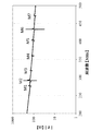
図2は右手系のオイラー角の座標系(φ,θ,Ψ)を示したものである。ここで、φはZ軸周りの回転角、θはX'軸(X軸をZ軸周りにφ回転したもの)周りの回転角、ΨはZ''軸(Z軸をX'軸周りにθ回転したもの)周りの回転角を示す。また、オイラー角(φ=0°,θ=0°,Ψ=0°)で表される水晶基板は、水晶のZ軸(光軸)に垂直な主面を有する回転Zカット基板となる。以下、弾性波素子11の各種解析に関してはこの座標系を用いて説明する。図3ではオイラー角(φ=0°,θ=125°,Ψ=38°)で表わされる水晶基板12内を伝搬する板波について、規格化された励振電極の膜厚Hs/λ=0、規格化された裏面電極の膜厚Hb/λ=0における分散曲線を示す。
FIG. 2 shows a right-handed Euler angle coordinate system (φ, θ, Ψ). Where φ is the rotation angle around the Z axis, θ is the rotation angle around the X ′ axis (the X axis is φ rotated around the Z axis), and ψ is the Z ″ axis (the Z axis is around the X ′ axis) This shows the rotation angle around. Further, the quartz substrate represented by Euler angles (φ = 0 °, θ = 0 °, ψ = 0 °) is a rotating Z-cut substrate having a principal surface perpendicular to the Z axis (optical axis) of the quartz. Hereinafter, various analyzes of the
図3で示される分散曲線は、縦波と横波が結合した板波あるいはラム波と呼ばれる振動モードである。これらの振動モードは表面波とは異なり、板厚に対しても周波数分散性を示し、位相速度が遅いものから速いものまで、それぞれ温度特性の異なる非常に多くの振動モードが存在する。本実施形態にあっては、後述する振動モードの温度特性の条件を満たすような位相速度が3500〜4500m/sに存在する板波を共振子に用いる。 The dispersion curve shown in FIG. 3 is a vibration mode called a plate wave or a Lamb wave in which a longitudinal wave and a transverse wave are combined. Unlike the surface wave, these vibration modes exhibit frequency dispersion with respect to the plate thickness, and there are a large number of vibration modes having different temperature characteristics from low to high phase velocity. In the present embodiment, a plate wave having a phase velocity of 3500 to 4500 m / s that satisfies the conditions of the temperature characteristics of the vibration mode described later is used for the resonator.
図4はθを変数とする右手系のオイラー角(φ=0°,θ,Ψ)による水晶基板12内を伝搬する振動モードの1次温度係数αを計算によって求めた結果である。図5はθを変数とする右手系のオイラー角(φ=0°,θ,Ψ)による水晶基板12内を伝搬する振動モードの2次温度係数βを計算によって求めた結果である。図4及び図5ともに、規格化板厚H/λ=1.18とし、励振電極と裏面電極の膜厚は無視して計算している。
FIG. 4 shows the result of calculating the first-order temperature coefficient α of the vibration mode propagating in the
図4及び図5によるとθ=125°,Ψ=38°近傍において、1次温度係数α×10−6が−1.0<α<+1.0、2次温度係数β×10−8が−1.0<β<+1.0の範囲内となっている。According to FIGS. 4 and 5, when θ = 125 ° and Ψ = 38 °, the primary temperature coefficient α × 10 −6 is −1.0 <α <+1.0, and the secondary temperature coefficient β × 10 −8 is It is in the range of −1.0 <β <+1.0.
図3の実線で示した振動モード曲線は、上記条件によって選択されたものであり、このときの振動モードの位相速度は3500〜4500m/sの範囲となる。なお、図4及び図5は解析値に基づくものであるため、実際には誤差等の影響もあり、1次温度係数α及び2次温度係数βは必ずしも0とはならない。このため、前記1次温度係数α及び2次温度係数βによる特性曲線が交差する点を中心値とし、この中心値が0に最も近いところを最適条件とした。 The vibration mode curve shown by the solid line in FIG. 3 is selected according to the above conditions, and the phase velocity of the vibration mode at this time is in the range of 3500 to 4500 m / s. Since FIGS. 4 and 5 are based on the analysis values, the primary temperature coefficient α and the secondary temperature coefficient β are not necessarily 0 due to the influence of errors and the like. For this reason, the point at which the characteristic curves of the primary temperature coefficient α and the secondary temperature coefficient β intersect is set as the center value, and the place where the center value is closest to 0 is set as the optimum condition.
次に、規格化された板厚をH/λ、規格化された励振電極膜厚をHs/λ、規格化された裏面電極膜厚をHb/λとした場合の最適な組み合わせ例を以下に示す。図6は、水晶基板のオイラー角が(φ=0°,θ=125.25°,Ψ=38°)、励振電極13及び裏面電極14の材質がAuであって、Hs/λ=0.015とした場合における1次温度係数αが0となるH/λと、Hb/λとの組み合わせを計算によって求めた結果である。この結果によれば、1次温度係数αが裏面電極14の膜厚によって変化することが確認できる。このため、回転角θ,Ψや板厚等を適時に調整することによって、最適な振動特性を得ることができる。
Next, an optimum combination example in which the standardized plate thickness is H / λ, the standardized excitation electrode film thickness is Hs / λ, and the standardized back electrode film thickness is Hb / λ is as follows. Show. In FIG. 6, the Euler angles of the quartz substrate are (φ = 0 °, θ = 125.25 °, Ψ = 38 °), the
表1は右手系のオイラー角を(φ=0°,θ=125.25°,Ψ=37.5°)として弾性波素子を製作した場合におけるモードごとの位相速度について、解析値と実験値を比較したものである。なお、比較対象とする振動モードは、電気機械結合係数K2が比較的大きく、測定の際にアドミッタンスの波形が十分に確認できるものを選択して行った。ここで、モード3が本発明において実際に使用するモードとなる。解析値と実験値とでは、モードごとにばらつきはあるものの、100m/s以内の誤差となっている。Table 1 shows analytical and experimental values for the phase velocity for each mode when an elastic wave device is manufactured with Euler angles of the right-handed system (φ = 0 °, θ = 125.25 °, Ψ = 37.5 °). Is a comparison. Incidentally, the vibration mode to be compared is, the electromechanical coupling factor K 2 is relatively large, the waveform of the admittance went select the one that can be confirmed sufficiently in the measurement. Here,

図7及び図8は、1次温度係数α及び2次温度係数βについての計算値と実験値を比較した結果を示したものである。Ψについては、板厚ごとに1次温度係数α×10−6が−1.0<α<+1.0の範囲内となるように調整している。また、励振電極及び裏面電極にAuを用い、Hs/λ=0.0015、Hb/λ=0.0045〜0.0070の条件設定で、1次温度係数α×10−6が−1.0<α<+1.0の範囲内となるように適宜調整を行った。7 and 8 show the results of comparing the calculated values and experimental values for the primary temperature coefficient α and the secondary temperature coefficient β. Ψ is adjusted so that the primary temperature coefficient α × 10 −6 falls within the range of −1.0 <α <+1.0 for each plate thickness. In addition, Au is used for the excitation electrode and the back electrode, and the primary temperature coefficient α × 10 −6 is −1.0 under the condition setting of Hs / λ = 0.015 and Hb / λ = 0.445 to 0.0070. <Α <+1.0 was appropriately adjusted to be within the range.
図7及び図8を見ると、誤差の範囲は僅かであり、計算結果が妥当であると考えられる。また、H/λ=1.18の近傍において、1次温度係数α×10−6が−1.0<α<+1.0、2次温度係数β×10−8が−1.0<β<+1.0の範囲内となり、良好な温度特性が得られることが確認できた。また、励振電極13及び裏面電極14の材質や膜厚を変更した場合は、それに応じて板厚や回転角θ,Ψを変える必要がある。なお、励振電極及び裏面電極には、Auの代わりにAlを使用した場合であっても同様の効果が得られる。7 and 8, the error range is small and the calculation result is considered to be appropriate. In the vicinity of H / λ = 1.18, the primary temperature coefficient α × 10 −6 is −1.0 <α <+1.0, and the secondary temperature coefficient β × 10 −8 is −1.0 <β. It was within the range of <+1.0, and it was confirmed that good temperature characteristics were obtained. Further, when the material and film thickness of the
上記結果から、θ,Ψ,H/λの各条件が、θ=124°〜130°、Ψ=37.5°〜38.5°、H/λ=1.10〜1.25の範囲に収まるように設計することによって、振動モードの位相速度が3500〜4500m/sで、1次温度係数α×10−6が−1.0<α<+1.0、2次温度係数β×10−8が−1.0<β<+1.0の範囲の温度特性となる良好な板波を発生させることが可能となる。なお、実際に弾性波素子11を製造する際における水晶基板12のカット角については、製造ばらつき等によって上記条件に必ずしも一致するものではない。このような製造ばらつき等を考慮すると、水晶基板12は、回転角がφ=0±10°、θ=110°〜140°、Ψ=30〜50°、H/λ=0.8〜1.4であれば本発明の効果を得ることができる。From the above results, the conditions of θ, Ψ, and H / λ are in the ranges of θ = 124 ° to 130 °, Ψ = 37.5 ° to 38.5 °, and H / λ = 1.10 to 1.25. By designing such that the phase velocity of vibration mode is 3500-4500 m / s, the primary temperature coefficient α × 10 −6 is −1.0 <α <+1.0, and the secondary temperature coefficient β × 10 − It is possible to generate a good plate wave in which 8 has temperature characteristics in the range of −1.0 <β <+1.0. Note that the cut angle of the
次に第2実施形態を上記図1に示した水晶基板12に基づいて説明する。この実施形態の水晶基板12は、右手系のオイラー角(φ=0°,θ=37.6°〜38.3°,Ψ=0°)によって、所定の板厚にカットされている。
Next, a second embodiment will be described based on the
図9ではオイラー角(φ=0°,θ=37.6°〜38.3°,Ψ=0°)で表わされる水晶基板12内を伝搬する板波について、Hs/λ=0、Hb/λ=0における分散曲線を示す。
In FIG. 9, for a plate wave propagating in the
図9で示される分散曲線は、縦波と横波が結合した板波あるいはラム波と呼ばれる振動モードである。これらの振動モードは表面波とは異なり板厚に対しても周波数分散性を示す。この分散曲線によって示されるように、板波には非常に多くのモードが存在するが、本実施形態では、位相速度が4500〜6000m/sとなる板波を振動モード(主振動)として選択した。一方、前記主振動の板波の下方に存在する板波は、主振動に影響を及ぼすおそれがある不要振動(副振動)である。 The dispersion curve shown in FIG. 9 is a vibration mode called a plate wave or a Lamb wave in which a longitudinal wave and a transverse wave are combined. Unlike the surface wave, these vibration modes exhibit frequency dispersion with respect to the plate thickness. As shown by this dispersion curve, there are a large number of modes in the plate wave. In this embodiment, a plate wave having a phase velocity of 4500 to 6000 m / s is selected as the vibration mode (main vibration). . On the other hand, the plate wave existing below the plate wave of the main vibration is unnecessary vibration (sub vibration) that may affect the main vibration.
このような多くの振動モードが存在する弾性波素子にあっては、主振動より音速が遅く、反射係数が主振動と一致し、且つ、実効的な電気機械結合係数Keff2が主振動より大きくなるような前記副振動が問題となる。この副振動に対して、Keff2を低く抑え込むことによって、等価直列抵抗を大きくし、発振させた際の異常発振を防止することができる。本発明では、前記K2を低減させる手段として、板波を励起させる励振電極13のメタライゼーションレシオηを最適な値に設定した。ここで、メタライゼーションレシオηとは、図1に示したように、励振電極13の電極指15bの幅Ltと、一方の電極指15bの内側から対向する他方の電極指16bの外側面までの幅Liとによって定義される値であり、次式のように表される。なお、波長λは同一のベース電極部15aに設けられる電極指15b間の幅で定義されている。
η=Lt/LiIn such an elastic wave element in which many vibration modes exist, the sound velocity is slower than that of the main vibration, the reflection coefficient coincides with the main vibration, and the effective electromechanical coupling coefficient Keff 2 is larger than that of the main vibration. Such sub-vibration becomes a problem. By suppressing Keff 2 to be low with respect to this secondary vibration, it is possible to increase the equivalent series resistance and prevent abnormal oscillation when oscillating. In the present invention, as a means for reducing the K 2 , the metallization ratio η of the
η = Lt / Li
前記K2は、圧電の性能の目安として広く使用されているものであるが、本発明のように、板波を発生させる弾性波素子にあっては、水晶基板の板厚を波長λ程度にまで薄くして使用されることから、励振電極13や裏面電極14の膜厚に大きく左右される。このため、共振周波数frと反共振周波数faから次式にて算出される実効的な電気機械結合係数Keff2を用いて、本発明に係る弾性波素子の圧電性について評価した。The K 2 is widely used as a measure of piezoelectric performance. However, in the case of an acoustic wave element that generates a plate wave as in the present invention, the thickness of the quartz substrate is set to about a wavelength λ. Therefore, it is greatly influenced by the film thickness of the
次に、右手系のオイラー角(φ=0°,θ=37.6°〜38.3°,Ψ=0°)にてカットされた水晶基板を対象とし、励振電極13及び裏面電極14にAuを用い場合において、メタライゼーションレシオη、H/λ、Hs/λ、Hb/λをそれぞれ変化させたときの主振動と副振動のKeff2を図10乃至図13に示す。Next, a quartz crystal substrate cut at a right-handed Euler angle (φ = 0 °, θ = 37.6 ° -38.3 °, ψ = 0 °) is used as an object, and the
図10は、H/λ=1.20,Hs/λ=0.005,Hb/λ=0.013として、メタライゼーションレシオηを変化させた場合における主振動と副振動のKeff2を示したものである。ηは、通常0.5付近に設定されるが、この0.5から所定の範囲にずらすことによって、副振動による発振を抑えることができる。そこで、本実施形態では、ηを所定の範囲で変化させ、その中で主振動の特性を大きく損なうことなく、副振動のKeff2を効果的に低減させることができる範囲を検証した。FIG. 10 shows Keff 2 of the main vibration and the secondary vibration when the metallization ratio η is changed with H / λ = 1.20, Hs / λ = 0.005, and Hb / λ = 0.003. Is. η is usually set to around 0.5, but by shifting from 0.5 to a predetermined range, oscillation due to side vibration can be suppressed. Therefore, in the present embodiment, η is changed within a predetermined range, and the range in which Keff 2 of the secondary vibration can be effectively reduced without significantly impairing the characteristics of the main vibration is verified.
図10は、右手系のオイラー角(φ,θ,Ψ)で規定される水晶基板12の各回転角がφ=0°,θ=37.6°〜38.3°,Ψ=0°の範囲に設定され、25℃でテイラー展開したときの1次温度係数α×10−6が−0.5<α<+0.5、2次温度係数β×10−8が−1.0<β<+1.0の範囲内にあるときの位相速度の板波を主振動とする弾性波素子について、励振電極13のメタライゼーションレシオηを調整しながら主振動及び副振動のKeff2を解析した。なお、前記条件の振動モードにおける位相速度は、4500〜6000m/s程度となる。FIG. 10 shows that the rotation angles of the
この結果から、メタライゼーションレシオηを0.6<η<0.9の範囲内に設定すれば、主振動に対して、副振動のKeff2を効果的に低減させることができることが確認された。これによって、副振動の等価直列抵抗を大きくし、上記選択された位相速度による主振動に影響を及ぼすことがない。From this result, it was confirmed that if the metallization ratio η is set within the range of 0.6 <η <0.9, the Keff 2 of the secondary vibration can be effectively reduced with respect to the main vibration. . This increases the equivalent series resistance of the secondary vibration and does not affect the main vibration due to the selected phase velocity.
次に、他の設計条件を変数として解析を行った結果を示す。図11は、メタライゼーションレシオη=0.5として、H/λを変化させた場合における主振動と副振動の実効的な電気機械結合係数Keff2を示したものである。この図11から、H/λが大きくなるにしたがって、主振動の前記Keff2が大きく低下する結果となった。この条件においては、H/λは1.25以下とすることが望ましい。Next, the results of analysis using other design conditions as variables are shown. FIG. 11 shows the effective electromechanical coupling coefficient Keff 2 of the main vibration and the sub vibration when the metallization ratio η = 0.5 and H / λ is changed. FIG. 11 shows that the Keff 2 of the main vibration greatly decreases as H / λ increases. Under these conditions, H / λ is preferably 1.25 or less.
図12は、メタライゼーションレシオη=0.5,H/λ=1.20,Hb/λ=0.013として、Hs/λを変化させた場合における主振動と副振動の実効的な電気機械結合係数Keff2を示したものである。また、図13は、メタライゼーションレシオη=0.5,H/λ=1.20,Hs/λ=0.005として、Hb/λを変化させた場合における主振動と副振動の実効的な電気機械結合係数Keff2を示したものである。図12及び図13からは、Hs/λ及びHb/λを変化させることによって、Keff2の値自体は変化するものの、Hs/λとHb/λの相対関係を大きく変えることができないことが確認された。なお、本実施形態では、励振電極13及び裏面電極14にAuを使用したが、Alを使用した場合であっても主振動と副振動の関係は略同様となる。FIG. 12 shows an effective electric machine of main vibration and sub vibration when the metallization ratio η = 0.5, H / λ = 1.20, Hb / λ = 0.133 and Hs / λ is changed. The coupling coefficient Keff 2 is shown. FIG. 13 shows that the main vibration and the sub vibration are effective when Hb / λ is changed with the metallization ratio η = 0.5, H / λ = 1.20, and Hs / λ = 0.005. The electromechanical coupling coefficient Keff 2 is shown. From FIG. 12 and FIG. 13, it is confirmed that the relative relationship between Hs / λ and Hb / λ cannot be changed greatly, although the value of Keff 2 itself changes by changing Hs / λ and Hb / λ. It was done. In this embodiment, Au is used for the
上記図11乃至図13の結果から、H/λに関しては、H/λが大きくなるにしたがって、主振動のKeff2が大きく低下することとなり、副振動を低減する効果が認められた。しかしながら、本発明による弾性波素子は、所定の位相速度と安定した高周波特性を得ることも目的としているため、上述したように、H/λは1.25以下とすることが望ましく、これを基準として、メタライゼーションレシオηを0.6<η<0.9の範囲で設定すればよい。なお、Hs/λ及びHb/λに関しては、副振動に対する直接的な効果は得られなかったが、高周波発振の実現及び周波数温度特性の微調整等において有効なパラメータとなっている。From the results shown in FIGS. 11 to 13, with respect to H / λ, as H / λ is increased, the Keff 2 of the main vibration is greatly reduced, and the effect of reducing the secondary vibration is recognized. However, since the elastic wave device according to the present invention is also intended to obtain a predetermined phase velocity and a stable high-frequency characteristic, as described above, it is desirable that H / λ is 1.25 or less, which is the standard. The metallization ratio η may be set in the range of 0.6 <η <0.9. Although Hs / λ and Hb / λ were not directly effective against sub-vibration, they are effective parameters for realizing high-frequency oscillation and fine-tuning frequency temperature characteristics.
次に、裏面電極14の膜厚と不要振動との関係を図14及び図15に基づいて説明する。図14に波長λ=11.78μm、板厚H=14.4μmにて構成した場合のインピーダンスZ波形の例を示す。異常発振の原因となる振動モード励振は、観測される波形のうち最も低い周波数とその次に低い周波数の2つ(M1,M2)であり、このときの主振動M6の周波数は433MHzである。異常発振の原因となる2つのモード(M1,M2)の位相特性は、図15に示すように、フイガーオブメリット(Figure of Merit)Mを基準として、裏面電極14の膜厚Hb/λに影響されることが実験結果によって証明された。
Next, the relationship between the film thickness of the
前記フイガーオブメリットMとは、水晶振動子のQ値を容量比γで割ったもので、機械的な振動子を電気端子から見たときの振動の強さを示している。一般的に、フイガーオブメリットMが2以上であれば、インダクティブになるため、コルピッツ発振回路よる発振が可能となるが、逆に2より小さくなると、リアクタンス成分が正、すなわちインダクティブとはならないため、コルピッツ発振回路を用いた発振ができなくなる。図15に示した実験結果によると、裏面電極14の材料にAuを用いた場合、0.001<Hb/λ<0.005の範囲であればフイガーオブメリットMが2より小さくなるので、モードM1,M2による不要振動が抑えられ、発振回路と組み合わせた場合の異常発振を防ぐことができる。
The “Figer of Merit M” is obtained by dividing the Q value of the crystal resonator by the capacitance ratio γ, and indicates the strength of vibration when the mechanical resonator is viewed from the electrical terminal. In general, if the Figger of Merit M is 2 or more, it becomes inductive, so oscillation by the Colpitts oscillation circuit is possible. The oscillation using the Colpitts oscillation circuit cannot be performed. According to the experimental results shown in FIG. 15, when Au is used as the material of the
本発明の弾性波素子11,21を製造する工程において、主振動のフイガーオブメリットMが2以上、且つ、不要振動のフイガーオブメリットMが2未満となる条件を設定し、この条件の下で水晶基板の板厚及び裏面電極の厚みを決定することで、不要振動による発振が有効に抑えられ、より安定した発振特性を得ることが可能となる。
In the process of manufacturing the
次に第3実施形態の弾性波素子21を図16乃至図25に基づいて説明する。
この実施形態の弾性波素子21は、図16に示すように、裏面側に一部が開口した凹部36を有する水晶基板22と、この水晶基板22の表面側に形成される励振電極23とで構成されている。また、前記水晶基板22の裏面側には、前記凹部36に沿って裏面電極24を形成することによって、周波数等の微調整が行えるように構成することもできる。Next, an
As shown in FIG. 16, the
前記水晶基板22は、凹部36が形成されていない状態のブロック体を、図2に示したような右手系のオイラー角(φ,θ,Ψ)によってカットし、その後にエッチングによって前記凹部36を形成したものである。本実施形態では、右手系のオイラー角(φ=0°,θ=37.6°〜38.3°,Ψ=0°)によって、所定の板厚にカットした水晶基板22を使用した。
In the
前記オイラー角によってカットされた水晶基板22は、エッチング加工によって、図17乃至図19に示したように、板厚Hが波長λと略同程度まで薄くしたY'面と平行な平板状の振動部31と、この振動部31の外周部を保持する保持部32とが一体化された形態となっている。前記振動部31の板厚Hは、隣接する電極指25b,26bの幅で規定される板波の波長λと同程度の厚みを有している。前記保持部32は、前記振動部31から下方に向けて所定の厚みに形成される側壁部33,34によって構成されている。前記板厚Hは、励振電極23及び裏面電極24の膜厚の関係に基づいて良好な温度特性を有するように調整される。
The
図17及び図19に示したように、側壁部33は、Z'面に対向しており、前記振動部31の板厚Hよりも広い幅W11に設定されている。また、図18及び図19に示したように、側壁部34は、X面に対向しており、前記側壁部33の幅W11より広い幅W21に設定されている。なお、前記幅W21に設定された側壁部34の反対側は開口部35となっている。
As shown in FIGS. 17 and 19, the
上記水晶基板22は、振動部31をエッチングによって薄く加工する際にできる形状となっており、各側壁部の幅はエッチングに対する耐性を得るために規定されている。一般的に回転Yカットによる水晶基板22に対して、図16に示したような凹部36をウェットエッチングによって加工する際には、水晶の異方性からくるエッチングレートの差から、図20及び図21に示すように、対向するZ'面とX面に比較的大きな傾斜面が形成されることが知られている。一般的な水晶振動子の場合にあっては、X面よりはZ'面の傾斜面の方が大きいため、このZ'面が問題となることが多いが、本発明のように、板波を伝搬させる弾性波素子21の場合は、Z'面のみならず、X面に形成される小さな傾斜面であっても振動特性に大きく影響する。
The
図19及び図21に示したように、上記加工上の理由によって、X面には側壁部34を設けず、開口部35とすることで、励振電極や反射器(図示せず)が形成される部分に傾斜面が形成されないようにした。これによって、前記振動部31のエッチングによって薄く平坦化された部分に励振電極23等を形成することができ、板波の伝搬特性を阻害することなくQ値を大きくすることができる。
As shown in FIGS. 19 and 21, due to the above processing reasons, excitation electrodes and reflectors (not shown) are formed by providing the opening
次に、上記構造による水晶基板を形成する工程を図20及び図21に示す。最初に、X軸、Y軸及びZ軸からなる三次元の結晶方位を有する水晶体から右手系のオイラー角(φ=0°、θ=37.6°〜38.3°、Ψ=0°)の範囲でカットされた水晶基板を用意する。この水晶基板の裏面に凹部36を形成する部分を露出させてエッチングマスクを形成した後、Y'面方向からウェットエッチング用の溶液を侵食させていくことで、Y'方向に深くエッチングさせる。そして、振動部31の厚みが所定の板厚Hとなったところでエッチング処理を終了する。
Next, a process of forming a quartz substrate having the above structure is shown in FIGS. First, a right-handed Euler angle (φ = 0 °, θ = 37.6 ° -38.3 °, ψ = 0 °) from a lens having a three-dimensional crystal orientation composed of an X axis, a Y axis, and a Z axis. Prepare a quartz substrate cut in the range of. After forming the etching mask by exposing the portion where the
図20はX面から見たエッチング過程を示したものであり、図21はZ'面から見たエッチング過程を示したものであるが、それぞれの回転面におけるエッチングは略同時進行する。水晶結晶22をウェットエッチングによって浸食させる際、その構造上、X面に対してはY'面への浸食と同時にZ'面側にも浸食が進み(図20(b)〜(d))、Z'面に対してはY'面への浸食と同時にX面側にも浸食が進むこととなる(図21(b)〜(d))。このため、図20(d)に示したように、X面から見たときの側壁部の幅が最小W12となる箇所があり、強度の点でこの最小幅W12が振動部31の板厚H以上とすることが望ましい。一方、図21(d)に示したように、Z'面から見たときの側壁部の幅が最小W22となる箇所があり、強度の点でこの最小幅W22が振動部31の板厚H以下となるような場合であれば、図21(e)に示したように、この最小幅となる側壁部をカットし、開口部としても、他方の側壁部が厚く加工されているため、強度を十分に保つことができる。
FIG. 20 shows the etching process as viewed from the X plane, and FIG. 21 shows the etching process as viewed from the Z ′ plane, but the etching on the respective rotating surfaces proceeds almost simultaneously. When the
次に、上記水晶基板22を用いて構成された弾性波素子21における温度特性等を検証した。通常、板波を発生させる構造の弾性波素子にあっては、規格化板厚H/λによって製造工程における周波数が大きく変動することが知られている。特に、一枚の水晶ウエハから多数個の弾性波素子を製造する場合にあっては、水晶ウエハの板厚が均一でないと、個々の取り出された弾性波素子において周波数のばらつきが生じてしまい、さらに、温度特性のばらつきも大きくなるといった問題があった。
Next, temperature characteristics and the like in the
本発明の弾性波素子21においては、励振電極23の裏面側に裏面電極24が設けられているので、励振電極23の膜厚と共に、裏面電極24の膜厚をトリミング調整することによって、1次温度係数α,2次温度係数β等によって規定される温度特性のばらつきを抑え、所定の位相速度となる最適な振動モードを得ることができる。
In the
本実施形態では、前述したオイラー角(φ=0°,θ=37.85°,Ψ=0°)の水晶基板22を用い、表面及び裏面にそれぞれ金(Au)の薄膜からなる励振電極23及び裏面電極24を形成した。図22は1次温度係数α及び2次温度係数βとカット角θとの関係を示したグラフであり、図23は1次温度係数α及び2次温度係数βとH/λとの関係を示したグラフである。また、図24は1次温度係数α及び2次温度係数βとHs/λとの関係を示したグラフであり、図25は1次温度係数α及び2次温度係数βとHb/λとの関係を示したグラフである。
In the present embodiment, the
図22乃至図25に示したように、θ、H/λ、Hs/λ、Hb/λの各条件が、
θ=37.6°〜38.3°、
1.07<H/λ<1.25、
0.00<Hs/λ<0.03、
0.00<Hb<0.05
の範囲に収まるように弾性波素子を設計することによって、
振動モードの位相速度が4500〜6000m/sとなり、
1次温度係数α×10−6が−1.0<α<+1.0、
2次温度係数β×10−8が−1.0<β<+1.0
の範囲内となる良好な板波を発生させることが可能となる。また、板厚がばらついた場合や周波数調整後においても1次温度係数αのばらつきを有効に抑えることが可能となる。As shown in FIGS. 22 to 25, each condition of θ, H / λ, Hs / λ, and Hb / λ is
θ = 37.6 ° -38.3 °,
1.07 <H / λ <1.25,
0.00 <Hs / λ <0.03,
0.00 <Hb <0.05
By designing the acoustic wave device to be in the range of
The phase speed of the vibration mode is 4500-6000 m / s,
Primary temperature coefficient α × 10 −6 is −1.0 <α <+1.0,
Secondary temperature coefficient β × 10 −8 is −1.0 <β <+1.0
It is possible to generate a favorable plate wave that falls within the range. In addition, even when the plate thickness varies or after frequency adjustment, it is possible to effectively suppress variations in the primary temperature coefficient α.
なお、実際に弾性波素子21を製造する際における水晶基板22のカット角については、製造ばらつき等によって上記条件に必ずしも一致するものではない。このような製造ばらつき等を考慮すると、水晶基板22は回転角がφ=0±10°、θ=35°〜40°、Ψ=0±10°、H/λ=1.00〜1.35の範囲であれば本発明の効果を得ることができる。
Note that the cut angle of the
上記第1実施形態の弾性波素子11では、図26(a)に示すように、裏面電極14が一対のIDT電極15,16全体を含むように水晶基板12の裏面全体に形成されているが、図26(b),(c)に示すように、各IDT電極15,16のベース電極部15a,16aを含まず、電極指15b,16bをカバーするエリア(位置及び範囲)に裏面電極14を形成することで、前述したような特性を有しつつ、水晶基板12に生じる並列容量の増加を抑えることが可能となる。
In the
前記水晶基板12の裏面全体に裏面電極を形成した場合、一対のIDT電極15,16間の配線パターンの引き回しによって、裏面電極14との間に静電容量が発生し、位相特性が悪化してしまうことが並列容量を増加させる原因となっている。そこで、板波を発生させる各電極指15b,16bをカバーする前記エリアに限定して裏面電極14を形成することで、水晶基板12における不要な静電容量を低減させることができ、これによって、位相特性の悪化を避けることができる。なお、図26(b),(c)の構成を第2実施形態の弾性波素子21に適用した場合でも同様の効果が得られる。
When the back electrode is formed on the entire back surface of the
図26(b)は裏面電極が1つの電極で構成されており、図26(c)は複数に分割されている構造である、図26(c)に示されるように、複数に分割する場合は分割した各電極間の隙間を板波の波長の1/8程度にするのが好ましい。 FIG. 26B shows a structure in which the back electrode is composed of one electrode, and FIG. 26C shows a structure in which the back electrode is divided into a plurality of parts. As shown in FIG. Preferably, the gap between the divided electrodes is set to about 1/8 of the plate wave wavelength.
11 弾性波素子
12 水晶基板
13 励振電極
14 裏面電極
15,16 IDT電極
15a,16a ベース電極部
15b,16b 電極指
21 弾性波素子
22 水晶基板
23 励振電極
24 裏面電極
25,26 IDT電極
25a,26a ベース電極部
25b,26b 電極指
31 振動部
32 保持部
33,34 側壁部
35 開口部
36 凹部
DESCRIPTION OF
Claims (9)
右手系のオイラー角(φ,θ,Ψ)で規定される回転角によってカットされ、板厚H/λが0.8<H/λ<1.4の範囲にある水晶基板と、この水晶基板の表面に板波を励振させる少なくとも1つの励振電極とを備える弾性波素子であって、
前記水晶基板は回転角がφ=0±10°、θ=110°〜140°、Ψ=30〜50°の範囲でカットされ、25℃でテイラー展開したときの1次温度係数α×10−6が−1.0<α<+1.0、2次温度係数β×10−8が−1.0<β<+1.0の範囲内にあり且つ位相速度が3500〜4500m/sとなる板波を振動モードとしたことを特徴とする弾性波素子。 The Y-axis and the Z-axis are rotated around the X-axis from the lens having a three-dimensional crystal orientation composed of the X-axis, the Y-axis, and the Z-axis.
A quartz substrate that is cut by a rotation angle defined by a right-handed Euler angle (φ, θ, Ψ) and has a thickness H / λ in a range of 0.8 <H / λ <1.4, and the quartz substrate An acoustic wave device comprising at least one excitation electrode for exciting a plate wave on the surface of
The quartz substrate is cut in the range of rotation angle φ = 0 ± 10 °, θ = 110 ° -140 °, ψ = 30-50 °, and Taylor temperature expansion at 25 ° C. α × 10 − 6 is -1.0 <α <+1.0,2 order temperature coefficient beta × 10 -8 is -1.0 <beta <range near Ri and phase velocity of +1.0 3500~4500m / s An acoustic wave device characterized in that a plate wave is in a vibration mode.
右手系のオイラー角(φ,θ,Ψ)で規定される回転角によってカットされ、板厚H/λが1.25以下の水晶基板と、この水晶基板の表面に板波を励振させる少なくとも1つの励振電極とを備える弾性波素子であって、
前記水晶基板は回転角がφ=0±10°、θ=35°〜40°、Ψ=0±10°の範囲でカットされ、25℃でテイラー展開したときの1次温度係数α×10−6が−1.0<α<+1.0、2次温度係数β×10−8が−1.0<β<+1.0の範囲内にあり且つ位相速度が4500m/s〜6000m/sの板波を振動モードとし、
前記励振電極は複数の電極指を有する櫛形電極によって形成され、各電極指間距離に対する一の電極指の幅の比で規定されるメタライゼーションレシオηを0.6<η<0.9の範囲内に設定することによって、前記振動モード以外の不要振動による異常発振を低減させたことを特徴とする弾性波素子。 The Y-axis and the Z-axis are rotated around the X-axis from the lens having a three-dimensional crystal orientation composed of the X-axis, the Y-axis, and the Z-axis.
A quartz substrate that is cut by a rotation angle defined by a right-handed Euler angle (φ, θ, ψ) and has a plate thickness H / λ of 1.25 or less , and at least one that excites a plate wave on the surface of the quartz substrate. An acoustic wave device comprising two excitation electrodes,
The quartz substrate is cut in the range of rotation angle φ = 0 ± 10 °, θ = 35 ° -40 °, ψ = 0 ± 10 °, and Taylor temperature expansion at 25 ° C. α × 10 − 6 -1.0 <α <+1.0,2 order temperature coefficient beta × 10 -8 is -1.0 <beta <range near Ri and phase velocity of +1.0 4500m / s~6000m / s The plate wave of
The excitation electrode is formed by a comb electrode having a plurality of electrode fingers, and a metallization ratio η defined by a ratio of the width of one electrode finger to a distance between the electrode fingers is in a range of 0.6 <η <0.9. The elastic wave device according to claim 1, wherein abnormal oscillation due to unnecessary vibration other than the vibration mode is reduced.
右手系のオイラー角(φ,θ,Ψ)における各回転角がφ=0±10°、θ=35°〜40°、Ψ=0±10°の範囲でカットされ、25℃でテイラー展開したときの1次温度係数α×10−6が−0.5<α<+0.5、2次温度係数β×10−8が−1.0<β<+1.0の範囲内で、位相速度が4500m/s〜6000m/sの板波を振動モードとし、板厚H/λが1.00<H/λ<1.35の範囲にある水晶基板と、
回転後のX軸をX’軸、Y軸をY’軸としたとき、前記Y’軸を法線方向とし、前記板波を励振させる少なくとも1つの励振電極が形成される薄板状の振動部と、
前記X軸及びZ’軸を法線方向とし、前記振動部よりも厚みを有して振動部の周囲を保持する保持部とによって一体形成され、
少なくとも縦波成分を有する振動モードを得ると共に、前記励振電極が複数の電極指を有する櫛形電極によって形成され、各電極指間距離に対する一の電極指の幅の比で規定されるメタライゼーションレシオηを0.6<η<0.9の範囲内に設定することによって、前記振動モード以外の不要振動による異常発振を低減させたことを特徴とする弾性波素子。 The Y-axis and the Z-axis are rotated around the X-axis from the lens having a three-dimensional crystal orientation composed of the X-axis, the Y-axis, and the Z-axis.
Each rotation angle in the right-handed Euler angles (φ, θ, ψ) is cut in the range of φ = 0 ± 10 °, θ = 35 ° -40 °, ψ = 0 ± 10 °, and Taylor development is performed at 25 ° C. When the primary temperature coefficient α × 10 −6 is −0.5 <α <+0.5 and the secondary temperature coefficient β × 10 −8 is within the range −1.0 <β <+1.0, the phase velocity A quartz substrate having a plate wave of 4500 m / s to 6000 m / s as a vibration mode and a thickness H / λ in a range of 1.00 <H / λ <1.35 ;
A thin plate-like vibrating portion in which at least one excitation electrode for exciting the plate wave is formed with the X ′ axis after rotation being the X ′ axis and the Y axis being the Y ′ axis, the Y ′ axis being the normal direction. When,
The X axis and the Z ′ axis are normal directions, and are formed integrally with a holding portion that has a thickness than the vibrating portion and holds the periphery of the vibrating portion,
A vibration mode having at least a longitudinal wave component is obtained, and the excitation electrode is formed by a comb-shaped electrode having a plurality of electrode fingers, and a metallization ratio η defined by a ratio of a width of one electrode finger to a distance between each electrode finger Is set in a range of 0.6 <η <0.9, and abnormal oscillation due to unnecessary vibration other than the vibration mode is reduced.
The back electrode for adjusting the frequency is formed on the back side of the quartz substrate corresponding to an area where the excitation electrode is formed by a comb electrode having a plurality of electrode fingers and the electrode fingers are provided. The elastic wave device according to any one of 1, 3 and 5 .
Priority Applications (1)
| Application Number | Priority Date | Filing Date | Title |
|---|---|---|---|
| JP2015524110A JP5835765B2 (en) | 2013-06-28 | 2014-06-26 | Elastic wave element |
Applications Claiming Priority (8)
| Application Number | Priority Date | Filing Date | Title |
|---|---|---|---|
| JP2013135673 | 2013-06-28 | ||
| JP2013135675 | 2013-06-28 | ||
| JP2013135672 | 2013-06-28 | ||
| JP2013135675 | 2013-06-28 | ||
| JP2013135673 | 2013-06-28 | ||
| JP2013135672 | 2013-06-28 | ||
| PCT/JP2014/066981 WO2014208664A1 (en) | 2013-06-28 | 2014-06-26 | Elastic wave device |
| JP2015524110A JP5835765B2 (en) | 2013-06-28 | 2014-06-26 | Elastic wave element |
Publications (2)
| Publication Number | Publication Date |
|---|---|
| JP5835765B2 true JP5835765B2 (en) | 2015-12-24 |
| JPWO2014208664A1 JPWO2014208664A1 (en) | 2017-02-23 |
Family
ID=52141990
Family Applications (1)
| Application Number | Title | Priority Date | Filing Date |
|---|---|---|---|
| JP2015524110A Active JP5835765B2 (en) | 2013-06-28 | 2014-06-26 | Elastic wave element |
Country Status (5)
| Country | Link |
|---|---|
| US (1) | US9800225B2 (en) |
| EP (1) | EP3016282B1 (en) |
| JP (1) | JP5835765B2 (en) |
| CN (1) | CN105393455B (en) |
| WO (1) | WO2014208664A1 (en) |
Families Citing this family (9)
| Publication number | Priority date | Publication date | Assignee | Title |
|---|---|---|---|---|
| JP2016152494A (en) * | 2015-02-17 | 2016-08-22 | 京セラクリスタルデバイス株式会社 | Crystal substrate and saw device using the same |
| WO2017077892A1 (en) * | 2015-11-02 | 2017-05-11 | 株式会社村田製作所 | Acoustic wave device |
| JP7033462B2 (en) * | 2018-02-19 | 2022-03-10 | NDK SAW devices株式会社 | Surface acoustic wave device |
| JP6939761B2 (en) * | 2018-12-21 | 2021-09-22 | 株式会社村田製作所 | Elastic wave device and electronic component module |
| CN110161371B (en) * | 2019-05-14 | 2020-05-19 | 华中科技大学 | Electric power system oscillation source positioning method based on negative damping torque |
| WO2021042344A1 (en) * | 2019-09-05 | 2021-03-11 | 刘宇浩 | Bulk acoustic wave resonance device and bulk acoustic wave filter |
| WO2021222433A1 (en) * | 2020-04-29 | 2021-11-04 | Murata Manufacturing Co., Ltd. | Elastic wave device and ladder filter |
| CN115428330B (en) | 2020-04-29 | 2023-09-12 | 株式会社村田制作所 | elastic wave device |
| GB2598165B (en) * | 2020-08-18 | 2022-08-24 | River Eletec Corp | Acoustic wave device |
Citations (6)
| Publication number | Priority date | Publication date | Assignee | Title |
|---|---|---|---|---|
| JP2002152007A (en) * | 2000-11-15 | 2002-05-24 | Hitachi Ltd | Lamb wave type elastic wave resonator |
| WO2005099089A1 (en) * | 2004-04-01 | 2005-10-20 | Toyo Communication Equipment Co., Ltd. | Surface acoustic device |
| JP2006217566A (en) * | 2005-01-07 | 2006-08-17 | Seiko Epson Corp | Lamb-wave high-frequency resonator |
| JP2008098974A (en) * | 2006-10-12 | 2008-04-24 | Seiko Epson Corp | Lamb wave type high frequency device |
| JP2010103803A (en) * | 2008-10-24 | 2010-05-06 | Epson Toyocom Corp | Surface acoustic wave resonator, surface acoustic wave oscillator, and surface acoustic wave module device |
| JP2011259348A (en) * | 2010-06-11 | 2011-12-22 | River Eletec Kk | Acoustic wave element |
Family Cites Families (19)
| Publication number | Priority date | Publication date | Assignee | Title |
|---|---|---|---|---|
| JPS5768925A (en) | 1980-10-17 | 1982-04-27 | Fujitsu Ltd | Piezoelectric device |
| JPS59210708A (en) | 1983-05-13 | 1984-11-29 | Matsushita Electric Ind Co Ltd | Manufacture of surface acoustic wave device |
| JPH04306668A (en) | 1991-04-04 | 1992-10-29 | Matsushita Electric Ind Co Ltd | Image formation device |
| JP2003258596A (en) | 2002-03-01 | 2003-09-12 | Yasuhiko Nakagawa | Lamb wave type high frequency resonator, oscillator employing the same, and high frequency signal generating method employing the lamb wave |
| CN1286266C (en) * | 2002-10-04 | 2006-11-22 | 精工爱普生株式会社 | Elestic surface wave device and modulation method of its temp. characteristic |
| JP2004274696A (en) * | 2002-10-04 | 2004-09-30 | Seiko Epson Corp | Surface acoustic wave device and temperature characteristic adjustment method of surface acoustic wave device |
| JP4465464B2 (en) | 2004-03-19 | 2010-05-19 | 国立大学法人山梨大学 | Lamb wave type elastic wave device |
| CN100539411C (en) | 2004-04-01 | 2009-09-09 | 爱普生拓优科梦株式会社 | Surface acoustic wave device |
| JP2006148622A (en) * | 2004-11-22 | 2006-06-08 | Seiko Epson Corp | Surface acoustic wave device and electronic equipment |
| CN100477514C (en) | 2005-01-07 | 2009-04-08 | 精工爱普生株式会社 | Lamb-wave high-frequency resonator |
| JP4315174B2 (en) * | 2006-02-16 | 2009-08-19 | セイコーエプソン株式会社 | Manufacturing method of lamb wave type high frequency device |
| JP4182993B2 (en) | 2006-06-30 | 2008-11-19 | Tdk株式会社 | MEMORY CONTROLLER, FLASH MEMORY SYSTEM HAVING MEMORY CONTROLLER, AND FLASH MEMORY CONTROL METHOD |
| JPWO2008114715A1 (en) * | 2007-03-15 | 2010-07-01 | 国立大学法人山梨大学 | Lamb wave type elastic wave device |
| US8384272B2 (en) * | 2008-01-30 | 2013-02-26 | Kyocera Corporation | Acoustic wave device and method for production of same |
| WO2010082571A1 (en) | 2009-01-15 | 2010-07-22 | 株式会社村田製作所 | Piezoelectric device and method for manufacturing piezoelectric device |
| CN102334289B (en) * | 2009-02-27 | 2015-10-07 | 精工爱普生株式会社 | SAW (Surface Acoustic Wave) resonator, surface acoustic wave oscillator and electronic equipment |
| JP2011171888A (en) | 2010-02-17 | 2011-09-01 | Seiko Epson Corp | Lamb wave resonator and oscillator |
| JP2012060418A (en) * | 2010-09-09 | 2012-03-22 | Seiko Epson Corp | Surface acoustic wave device, electronic apparatus and sensor device |
| JP5768925B2 (en) | 2014-11-12 | 2015-08-26 | 株式会社オートネットワーク技術研究所 | connector |
-
2014
- 2014-06-26 WO PCT/JP2014/066981 patent/WO2014208664A1/en active Application Filing
- 2014-06-26 JP JP2015524110A patent/JP5835765B2/en active Active
- 2014-06-26 US US14/901,584 patent/US9800225B2/en active Active
- 2014-06-26 EP EP14817110.1A patent/EP3016282B1/en active Active
- 2014-06-26 CN CN201480033294.6A patent/CN105393455B/en active Active
Patent Citations (6)
| Publication number | Priority date | Publication date | Assignee | Title |
|---|---|---|---|---|
| JP2002152007A (en) * | 2000-11-15 | 2002-05-24 | Hitachi Ltd | Lamb wave type elastic wave resonator |
| WO2005099089A1 (en) * | 2004-04-01 | 2005-10-20 | Toyo Communication Equipment Co., Ltd. | Surface acoustic device |
| JP2006217566A (en) * | 2005-01-07 | 2006-08-17 | Seiko Epson Corp | Lamb-wave high-frequency resonator |
| JP2008098974A (en) * | 2006-10-12 | 2008-04-24 | Seiko Epson Corp | Lamb wave type high frequency device |
| JP2010103803A (en) * | 2008-10-24 | 2010-05-06 | Epson Toyocom Corp | Surface acoustic wave resonator, surface acoustic wave oscillator, and surface acoustic wave module device |
| JP2011259348A (en) * | 2010-06-11 | 2011-12-22 | River Eletec Kk | Acoustic wave element |
Also Published As
| Publication number | Publication date |
|---|---|
| WO2014208664A1 (en) | 2014-12-31 |
| EP3016282A4 (en) | 2016-07-13 |
| CN105393455B (en) | 2017-04-12 |
| CN105393455A (en) | 2016-03-09 |
| US9800225B2 (en) | 2017-10-24 |
| EP3016282A1 (en) | 2016-05-04 |
| EP3016282B1 (en) | 2018-08-01 |
| JPWO2014208664A1 (en) | 2017-02-23 |
| US20160204760A1 (en) | 2016-07-14 |
Similar Documents
| Publication | Publication Date | Title |
|---|---|---|
| JP5835765B2 (en) | Elastic wave element | |
| JP4591800B2 (en) | Surface acoustic wave device and surface acoustic wave oscillator | |
| CN102403979B (en) | Surface acoustic wave device, electronic apparatus, and sensor apparatus | |
| CN102403975B (en) | Surface acoustic wave device, electronic apparatus, and sensor apparatus | |
| JP2007300287A (en) | Surface acoustic wave element, surface acoustic wave device, and electronic apparatus | |
| JP5648908B2 (en) | Vibration device, oscillator, and electronic device | |
| JP3622202B2 (en) | Method for adjusting temperature characteristics of surface acoustic wave device | |
| JP4858730B2 (en) | Surface acoustic wave device and surface acoustic wave oscillator | |
| JP5141856B2 (en) | Method for manufacturing surface acoustic wave device and surface acoustic wave device | |
| JP4645957B2 (en) | Surface acoustic wave element and surface acoustic wave device | |
| WO2020095586A1 (en) | Elastic wave device, duplexer, and communication device | |
| JP2006295311A (en) | Surface acoustic wave element chip and surface acoustic wave device | |
| JPH09298446A (en) | Surface acoustic wave device and its design method | |
| JP5563378B2 (en) | Elastic wave element | |
| JP4465464B2 (en) | Lamb wave type elastic wave device | |
| JP2020080519A (en) | Surface acoustic wave element | |
| TWI747636B (en) | Acoustic wave device | |
| JP2009077209A (en) | Surface acoustic wave resonator | |
| JP2009027671A (en) | Sh type bulk wave resonator | |
| JP2003309446A (en) | Piezoelectric vibrator | |
| JP2005184340A (en) | Surface acoustic wave chip | |
| JP2020141382A (en) | Surface acoustic wave resonator | |
| JP2011114397A (en) | Lamb wave type acoustic wave element | |
| JP2015084535A (en) | Transversal type surface acoustic wave device, surface acoustic wave oscillator, and electronic apparatus | |
| JPS632413A (en) | Elastic surface wave resonator |
Legal Events
| Date | Code | Title | Description |
|---|---|---|---|
| TRDD | Decision of grant or rejection written | ||
| A01 | Written decision to grant a patent or to grant a registration (utility model) |
Free format text: JAPANESE INTERMEDIATE CODE: A01 Effective date: 20151006 |
|
| A61 | First payment of annual fees (during grant procedure) |
Free format text: JAPANESE INTERMEDIATE CODE: A61 Effective date: 20151027 |
|
| R150 | Certificate of patent or registration of utility model |
Ref document number: 5835765 Country of ref document: JP Free format text: JAPANESE INTERMEDIATE CODE: R150 |
|
| R250 | Receipt of annual fees |
Free format text: JAPANESE INTERMEDIATE CODE: R250 |
|
| R250 | Receipt of annual fees |
Free format text: JAPANESE INTERMEDIATE CODE: R250 |
|
| R250 | Receipt of annual fees |
Free format text: JAPANESE INTERMEDIATE CODE: R250 |
|
| R250 | Receipt of annual fees |
Free format text: JAPANESE INTERMEDIATE CODE: R250 |
|
| R250 | Receipt of annual fees |
Free format text: JAPANESE INTERMEDIATE CODE: R250 |
|
| R250 | Receipt of annual fees |
Free format text: JAPANESE INTERMEDIATE CODE: R250 |