JP5829150B2 - Lighting device - Google Patents
Lighting device Download PDFInfo
- Publication number
- JP5829150B2 JP5829150B2 JP2012047837A JP2012047837A JP5829150B2 JP 5829150 B2 JP5829150 B2 JP 5829150B2 JP 2012047837 A JP2012047837 A JP 2012047837A JP 2012047837 A JP2012047837 A JP 2012047837A JP 5829150 B2 JP5829150 B2 JP 5829150B2
- Authority
- JP
- Japan
- Prior art keywords
- led
- circuit board
- light
- led device
- emitting
- Prior art date
- Legal status (The legal status is an assumption and is not a legal conclusion. Google has not performed a legal analysis and makes no representation as to the accuracy of the status listed.)
- Active
Links
Images


Classifications
-
- H—ELECTRICITY
- H01—ELECTRIC ELEMENTS
- H01L—SEMICONDUCTOR DEVICES NOT COVERED BY CLASS H10
- H01L2224/00—Indexing scheme for arrangements for connecting or disconnecting semiconductor or solid-state bodies and methods related thereto as covered by H01L24/00
- H01L2224/01—Means for bonding being attached to, or being formed on, the surface to be connected, e.g. chip-to-package, die-attach, "first-level" interconnects; Manufacturing methods related thereto
- H01L2224/42—Wire connectors; Manufacturing methods related thereto
- H01L2224/47—Structure, shape, material or disposition of the wire connectors after the connecting process
- H01L2224/48—Structure, shape, material or disposition of the wire connectors after the connecting process of an individual wire connector
- H01L2224/4805—Shape
- H01L2224/4809—Loop shape
- H01L2224/48091—Arched
-
- H—ELECTRICITY
- H01—ELECTRIC ELEMENTS
- H01L—SEMICONDUCTOR DEVICES NOT COVERED BY CLASS H10
- H01L2224/00—Indexing scheme for arrangements for connecting or disconnecting semiconductor or solid-state bodies and methods related thereto as covered by H01L24/00
- H01L2224/01—Means for bonding being attached to, or being formed on, the surface to be connected, e.g. chip-to-package, die-attach, "first-level" interconnects; Manufacturing methods related thereto
- H01L2224/42—Wire connectors; Manufacturing methods related thereto
- H01L2224/47—Structure, shape, material or disposition of the wire connectors after the connecting process
- H01L2224/48—Structure, shape, material or disposition of the wire connectors after the connecting process of an individual wire connector
- H01L2224/481—Disposition
- H01L2224/48135—Connecting between different semiconductor or solid-state bodies, i.e. chip-to-chip
- H01L2224/48137—Connecting between different semiconductor or solid-state bodies, i.e. chip-to-chip the bodies being arranged next to each other, e.g. on a common substrate
-
- H—ELECTRICITY
- H01—ELECTRIC ELEMENTS
- H01L—SEMICONDUCTOR DEVICES NOT COVERED BY CLASS H10
- H01L2924/00—Indexing scheme for arrangements or methods for connecting or disconnecting semiconductor or solid-state bodies as covered by H01L24/00
- H01L2924/15—Details of package parts other than the semiconductor or other solid state devices to be connected
- H01L2924/181—Encapsulation
Landscapes
- Led Device Packages (AREA)
- Fastening Of Light Sources Or Lamp Holders (AREA)
- Non-Portable Lighting Devices Or Systems Thereof (AREA)
Description
本発明は、発光ダイオード(LED)を実装した回路基板を備える電球型の照明装置に関する。 The present invention relates to a light bulb-type lighting device including a circuit board on which a light emitting diode (LED) is mounted.
近年、消費電力の多い白熱電球の代替として、消費電力が少なく、白熱電球と形状が類似した電球型LEDランプが普及してきている。しかしながら、電球型LEDランプから出射する光は指向性が強いため口金側が暗くなってしまっていた。この対策として例えば特許文献1の図1に示された照明器具(電球型の照明装置)がある。 In recent years, as an alternative to incandescent lamps with high power consumption, light bulb-type LED lamps with low power consumption and similar in shape to incandescent lamps have become widespread. However, the light emitted from the bulb-type LED lamp has a strong directivity, so the base side is dark. As a countermeasure, for example, there is a lighting fixture (bulb-type lighting device) shown in FIG.
特許文献1の図1を図9に再掲示し更に詳しく説明する。図9は従来の電球型LEDランプの全体構成を一部縦断面で示す正面図である。ランプ1は、金属製の外郭部材であるカバー2、光源装置11、この光源装置11を被覆する光源カバー21(グローブともいう)、点灯回路25、口金31を具備している。光源装置11は発光部12(LED)と導光体17を備えている。導光体17の頂上には反射面20があり、その下に出射部19がある。
FIG. 1 of Patent Document 1 is shown again in FIG. 9 and will be described in more detail. FIG. 9 is a front view showing a part of the entire configuration of a conventional light bulb type LED lamp in a longitudinal section. The lamp 1 includes a cover 2 that is a metal outer member, a light source device 11, a light source cover 21 (also referred to as a globe) that covers the light source device 11, a
発光部12から導光体17内へ入射した光は反射面20へ導光され、反射面20により反射された光の一部が横方向へ出射する。この横方向へ出射した光は光源カバー21の頂端側の球面により反射されて発光部12側へ投光される。この結果、一般照明用電球と同様に口金31側にも投光することができる。
The light that has entered the light guide 17 from the light emitting unit 12 is guided to the reflecting surface 20, and a part of the light reflected by the reflecting surface 20 is emitted in the lateral direction. The light emitted in the lateral direction is reflected by the spherical surface on the top end side of the
図9の照明器具は光源カバー21の内側に光源装置11に含まれる導光体17を付加し、配光特性を改善したものということができる。しかしながら導光体17を付加することは部品増とともに組み立て工数増を招くだけでなく、構造の複雑化も課題となる。例えば導光体17の質量が上部に存在するため、導光体17を発光部基板13に固定させる構造は強固なものにしなくてはならない。また導光体17は形状が複雑なうえ、透明樹脂部と反射板20との2体構造でもある。反射板20も頂点側に光を出射させるため半透過反射板にしたほうが良い。以上のようにグローブの内部を立体的な構造にすると、これに付随し様々な問題が生じることが多い。すなわち光源となるLEDを実装した状態の回路基板をできるかぎり平坦にすることが望まれる。
9 can be said to have improved light distribution characteristics by adding the light guide 17 included in the light source device 11 inside the
そこで本発明は、上記課題に鑑みてなされたものであり、口金方向に広がる配光分布を持たせてもグローブ内の構造が立体的にならない電球型の照明装置を提供することを目的としている。 Therefore, the present invention has been made in view of the above problems, and an object of the present invention is to provide a light bulb-type lighting device in which the structure in the globe does not become three-dimensional even if the light distribution is widened in the direction of the base. .
光源となるLEDを実装した回路基板を備える電球型の照明装置において、
前記複数のLEDのうち前記回路基板の中央部に実装する前記LEDがベアチップのLEDダイであるか、又は表面実装型LED装置であり、
前記回路基板周辺部に実装する前記LEDが側面発光型LED装置であり、
前記回路基板が前記側面発光型LED装置の実装部に切り欠き部がある
ことを特徴とする。
In a bulb-type lighting device including a circuit board on which an LED serving as a light source is mounted,
Of the plurality of LEDs, the LED mounted on the center of the circuit board is a bare-chip LED die, or a surface-mounted LED device,
Ri said LED is a side emitting type LED device der to be mounted on the circuit board periphery,
The circuit board has a notch in a mounting portion of the side-emitting LED device .
本発明の照明装置はグローブ内に複数のLEDを実装した回路基板を備えている。LEDは少なくとも二つに分類される。一方のLEDは、回路基板の中央に実装され、主に回路基板の垂直方向に光を放射するLEDであり、他方のLEDは、回路基板の周辺に配置され、主に回路基板の水平に光を放射するLEDである。このようにして回路基板の中央部に実装されたLEDと、回路基板の周辺に実装されたLEDとが分担して回路基板の垂直方向と水平方向に光を放射する。この結果、本発明の照明装置は広い配光分布が得られ、LEDを実装した状態の回路基板は平面的になっている。また回路基板中央部に実装するLEDはベアチップであるLEDダイでも表面実装型LED装置であってもよい。 The lighting device of the present invention includes a circuit board on which a plurality of LEDs are mounted in a globe. LEDs are classified into at least two. One LED is mounted at the center of the circuit board and emits light mainly in the vertical direction of the circuit board, and the other LED is arranged around the circuit board and mainly emits light horizontally on the circuit board. It is LED which radiates. In this way, the LED mounted on the central portion of the circuit board and the LED mounted on the periphery of the circuit board share and emit light in the vertical and horizontal directions of the circuit board. As a result, the illumination device of the present invention has a wide light distribution, and the circuit board on which the LEDs are mounted is planar. The LED mounted on the center of the circuit board may be an LED die that is a bare chip or a surface-mounted LED device.
前記側面発光型LED装置は、前記回路基板に対し垂直なサブマウント基板と、上面及び側面を覆い底面が開いた反射樹脂と、前記サブマウント基板に実装されたLEDダイと、該LEDダイを被覆する被覆樹脂とを備えていても良い。
The side view LED device, said circuit perpendicular submount substrate relative to the substrate, and the reflecting resin which upper and side surfaces infusible covering bottom open, the LED die mounted on the sub-mount substrate, the LED die You may provide the coating resin to coat | cover.
前記被覆樹脂が蛍光体を含有していても良い。 The coating resin may contain a phosphor.
前記側面発光型LED装置に含まれるLEDダイは、上面及び側面にそれぞれ上面反射層及び側面蛍光部材を備え、底面に接続用電極が付着し、該接続用電極が前記回路基板の配線電極と接続していても良い。 The LED die included in the side light emitting LED device includes an upper surface reflection layer and a side surface fluorescent member on the upper surface and the side surface, and a connection electrode is attached to the bottom surface, and the connection electrode is connected to the wiring electrode of the circuit board You may do it.
以上のように本発明の照明装置は、2種類のLEDで回路基板の垂直及び水平方向に光を放射させることにより広い配光分布が得られる。このときパッケージ状態のLED装置かベアチップ状態のLEDダイを回路基板に実装するだけなので、回路基板が比較的平坦になる。この結果、本発明の照明装置は、口金方向に広がる配光分布を持たせてもグローブ内の構造が立体的にならない。 As described above, the illumination device of the present invention can obtain a wide light distribution by emitting light in the vertical and horizontal directions of the circuit board with two types of LEDs. At this time, since the LED device in the package state or the LED die in the bare chip state is simply mounted on the circuit substrate, the circuit substrate becomes relatively flat. As a result, the illumination device of the present invention does not have a three-dimensional structure in the globe even if it has a light distribution that spreads in the direction of the base.
以下、添付図1〜8を参照しながら本発明の好適な実施形態について詳細に説明する。なお図面の説明において、同一または相当要素には同一の符号を付し、重複する説明は省略する。また説明のため部材の縮尺は適宜変更している。さらに特許請求の範囲に記載した発明特定事項との関係をカッコ内に記載している。 Hereinafter, preferred embodiments of the present invention will be described in detail with reference to FIGS. In the description of the drawings, the same or equivalent elements will be denoted by the same reference numerals, and redundant description will be omitted. For the sake of explanation, the scale of the members is changed as appropriate. Furthermore, the relationship with the invention specific matter described in the claims is described in parentheses.
一般に照明装置に組み込まれる回路基板には、パッケージ状態のLEDを実装する場合と、ベアチップ状態のLEDを実装する場合とがある。パッケージ状態のLEDとは、ベアチップのLED素子にサブマウウント基板を取り付けたり、ベアチップのLED素子を樹脂などで被覆したりしたものである。そこで本明細書ではパッケージ状態のLEDをLED装置と呼び、ベアチップ状態のLEDをLEDダイと呼び区別する。さらに回路基板に実装したときに、配光分布が回路基板に対し垂直方向に強く現れるLED装置を表面実装型LED装置と呼び、配光分布が回路基板に対し水平方向に強く現れるLED装置を側面発光型LED装置と呼び区別する。なおLED装置に含まれるベアチップのLED素子もLEDダイと呼ぶ。
(第1実施形態)
In general, a packaged LED and a bare chip LED are mounted on a circuit board incorporated in a lighting device. The packaged LED is a LED in which a submount substrate is attached to a bare chip LED element, or a bare chip LED element is covered with a resin or the like. Therefore, in this specification, packaged LEDs are referred to as LED devices, and bare-chip LEDs are referred to as LED dies. Furthermore, when mounted on a circuit board, an LED device in which the light distribution distribution appears strongly in the vertical direction with respect to the circuit board is called a surface-mounted LED device. This is called a light-emitting LED device. A bare-chip LED element included in the LED device is also called an LED die.
(First embodiment)
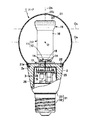
図1〜4を用いて本発明の第1実施形態を説明する。先ず図1により本実施形態の照明装置である電球型LEDランプ40の全体構成を説明する。図1は電球型LEDランプ40の全体構成を一部縦断面で示す正面図である。外郭部材であるカバー46の上部には回路基板44が搭載されている。回路基板44の中央部には表面実装型LED装置42(LED)が実装され、回路基板44の周辺部には側面発光型LED装置43(LED)が実装されている。カバー46には空洞があり、この空洞内に点灯回路45が収納されている。またカバー46の周辺部でグローブ41が固定され、カバー46下部では口金47が連結している。カバー46は、これらの部材を支持するだけでなくLED(表面実装型LED装置42及び側面発光型LED装置43)の放熱に係わっており、熱伝導性の良い樹脂またはアルミニウムからなる。カバー46の上端部は断面が台形になっており、側面発光型LED装置43から放射される光が口金47側に向かい易くしている。
1st Embodiment of this invention is described using FIGS. First, an overall configuration of a light bulb
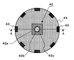
次に図2を用いて電球型LEDランプ40に含まれる回路基板44について説明する。図2は回路基板44の平面図である。回路基板44は円形であり、中央部に表面実装型LED装置42が実装され、周辺部に8個の側面発光型LED装置43が実装されている。表面実装型LED装置42には、サブマウント基板42aとダム材42b、被覆樹脂42cが見える。
Next, the
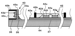
次に図3と図4を用いて回路基板44に実装されたLEDについて説明する。図3は図2のAA線に沿って描いた回路基板44と、回路基板44上に実装された表面実装型LED装置42、側面発光型LED装置43の断面図であり、図4は側面発光型LED装置43の側面図である。回路基板44の両端(右端は図示していない)には側面発光型LED装置43が実装され、中央部には表面実装型LED装置42が実装されている。回路基板44はアルミベース上に絶縁膜を備えたアルミ基板であり、その上に配線電極36,37が形成されている。
Next, the LED mounted on the
まず側面発光型LED装置43について説明する。側面発光型LED装置43は、回路基板44に対し垂直なサブマウント基板43aと、底面及び上面、側面を囲む枠状の反射樹脂43bと、サブマウント基板43aに実装されたLEDダイ43eと、LEDダイ43eを被覆する被覆樹脂43cからなる。LEDダイ43eはサブマウント基板43aにダイボンディングされ、ワイヤ43dによりサブマウント基板43aの電極(図示せず)と電気的に接続している。被覆樹脂43cはシリコーン樹脂であり蛍光体を含有している。また側面発光型LED装置43は回路基板44上の配線電極36と半田35で接続する。なお側面発光型LED装置43の光出射面からは、図4に示されるように枠状の反射樹
脂43bとその内側にある被覆樹脂43cが見える。
First, the side-emitting
次に表面実装型LED装置42について説明する。図3に示すように表面実装型LED装置42は、サブマウント基板42aと、ダム材42bと、被覆樹脂42cと、複数のLEDダイ42f,42gを含んでいる。サブマウント基板42a上に形成されたダム材42bの内側の領域では、LEDダイ42f,42gがサブマウント基板42aにダイボンディングされ、蛍光体を含有する被覆樹脂42cにより被覆されている。なおダム材42bの内側の領域には多数のLEDダイが実装されているが、説明のためLEDダイ42f,42gだけを示している。ワイヤ42dによりLEDダイ42fとサブマウント基板42a上の電極(図示せず)が電気的に接続し、ワイヤ42eによりLEDダイ42fとLEDダイ42gが直列接続する。表面実装型LED装置42は回路基板44の中央部に搭載される。
Next, the surface mount
表面実装型LED装置42が回路基板44に対し垂直方向に強い配光分布を持ち、側面発光型LED装置43が回路基板44に対し水平方向に強い配光分布を持つ。この結果、電球型ランプ40(図1参照)は口金47(図1参照)方向にも配光分布が広がる。このとき回路基板44上には表面実装型LED装置42と側面発光型LED装置43だけしか実装されてないので、グローブ41(図1参照)内が平面的な構造になっている。なお回路基板44には表面実装型LED装置42が1個だけ実装されていたが、明るさを増す必要がある場合は表面実装型LED装置42を複数実装すれば良い。
(第2実施形態)
The surface-mounted
(Second Embodiment)
第1実施形態の照明装置(電球型LEDランプ40)に含まれる回路基板44では、回路基板44の垂直方向の配光を担うLEDは表面実装型LED装置42であった。しかしながら回路基板44の垂直方向の配光を担うLEDにはベアチップであるLEDダイを使っても良い。また回路基板44に実装された側面発光型LED装置43は反射樹脂43b(図3参照)が枠状であるため水平方向より下側の配光分布が充分でないことがある。そこで図5と図6により、回路基板にLEDダイを直接実装し、さらに回路基板の水平方向より下側の配光分布を改善したものとして、本発明の第2実施形態について説明する。なお本実施形態における照明装置の外観は図1に示した電球型LEDランプ40と等しい。
In the
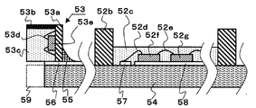
図5は、本実施形態の照明装置に含まれる回路基板54と、回路基板54に実装されたLEDダイ53f,53g、側面発光型LED装置53の断面図であり、図6は側面発光型LED装置53の側面図である。回路基板54の両端(右端は図示していない)には側面発光型LED装置53が実装され、回路基板54の中央部にはLEDダイ52f,52gが実装されている。なお回路基板54の中央部には多数のLEDダイが実装されているが、説明のためLEDダイ52f,52gだけを示している。回路基板54はアルミベース上に絶縁膜を備えたアルミ基板であり、その上に配線電極56,57,58が形成されている。回路基板54の平面形状は一部に切り欠きがある円形であり、ダム材52bは回路基板54と同心円になる。
FIG. 5 is a cross-sectional view of the
まず側面発光型LED装置53及びその周辺の回路基板54について説明する。側面発光型LED装置53は、回路基板54に対し垂直なサブマウント基板53aと、上面及び側面を覆う反射樹脂53bと、サブマウント基板53aに実装されたLEDダイ53eと、LEDダイ53eを被覆する被覆樹脂53cからなる。LEDダイ53eはサブマウント基板53aにダイボンディングされ、ワイヤ53dによりサブマウント基板53aの電極(図示せず)と電気的に接続している。被覆樹脂53cはシリコーン樹脂であり蛍光体を含有している。また側面発光型LED装置53は回路基板54上の配線電極56と半田55で接続する。なお側面発光型LED装置53の光出射面からは、図6に示されるように、下側が開いたコの字形の反射樹脂53bとその内側の被覆樹脂53cが見える。
First, the side-emitting
回路基板54は、前述したように図2の回路基板44と同様に円形を基本としているが、側面発光型LED装置53の下側を切り欠いている。図3では点線により回路基板54の切り欠き部59を示している。側面発光型LED装置53は、底部に反射樹脂がないこと及び回路基板54に切り欠き部59があることにより、口金47(図1参照)方向に配光分布を広げている。
As described above, the
次にLED装置52f、52gについて説明する。図5に示すように回路基板54の中央部にはダム材52bで囲まれた領域があり、この領域においてLED装置52f、52gが配線電極58上にダイボンディングされ、蛍光体を含有する被覆樹脂52cにより被覆されている。ワイヤ52dによりLEDダイ52fと配線電極57が電気的に接続し、ワイヤ52eによりLEDダイ52fとLEDダイ52gが直列接続している。
(第3実施形態)
Next, the
(Third embodiment)
第1実施形態及び第2実施形態に含まれる表面実装型LED装置42及び側面発光型LED装置43,53は、サブマウント基板42a,43a,53aを備えていた。これに対しサブマウント基板を省いてLED装置の構造を簡単化しても良い。そこで図7と図8によりサブマウント基板を省いて構造を簡単化したLED装置を用いた例として本発明の第3実施形態を説明する。なお本実施形態における照明装置の外観は図1に示した電球型LEDランプ40と等しい。
The surface-mounted
図7は、第3実施形態の照明装置に含まれる回路基板74と、回路基板74に実装された側面発光型LED装置73及び表面実装型LED装置72の断面図であり、図8は、(a)が側面発光型LED装置73から上面反射層73aを剥がした状態の平面図、(b)が表面実装型LED装置72の上面蛍光体層72aを剥がした状態の平面図である。回路基板74の両端(右端は図示していない)には側面発光型LED装置73が実装され、回路基板74の中央部には表面実装型LED装置72が実装されている。なお回路基板74の中央部には多数の表面実装型LED装置72が実装されているが、説明のため2個だけ示している。回路基板74はアルミベース上に絶縁膜を備えたアルミ基板であり、その上に配線電極75,76が形成されている。回路基板74の平面形状は図2の回路基板44と同様に円形である。回路基板44と回路基板74を比較すると、回路基板44における表面実装型LED装置42が回路基板74では多数の表面実装型LED装置72の置き換わり、同様に側面発光型LED装置43が側面発光型LED装置73に置き換わる。
FIG. 7 is a cross-sectional view of the circuit board 74 included in the lighting device of the third embodiment, the side-emitting
まず回路基板74の左端に実装された側面発光型LED装置73について説明する。側面発光型LED装置73に含まれるLEDダイ73cは、上面及び側面にそれぞれ上面反射層73a及び側面蛍光部材73bを備え、底面に2個の接続用電極73dが付着している。図8(a)に示されるように側面蛍光部材73bはLEDダイ73cの周囲を枠状に取り囲んでいる。また接続用電極73dは回路基板74の配線電極75と接続している。なおLEDダイ73cは厚さが80〜120μm程度のサファイア基板(図示せず)の下面に、厚さが10μm弱の半導体層(図示せず)を備えている。上面反射層73aはシリコーン樹脂に酸化チタンやアルミナなどの反射性微粒子を混練し硬化させたものである。
First, the side-emitting
側面発光型LED装置73においてLEDダイ73cに含まれる半導体層が発光すると、発光はサファイア基板側に入射する(なお半導体層の下部には金属反射層がある)。サファイア基板に入射した光はLEDダイ73cの上面反射層73aによりサファイア基板の側面から出射する。サファイア基板の側面から出射した光は側面蛍光部材73bで白色化され、回路基板74の水平方向を中心に光を放射する。
When the semiconductor layer included in the
次に回路基板74の中央部に実装された表面実装型LED装置72について説明する。
表面実装型LED装置72に含まれるLEDダイ72cは、上面及び側面にそれぞれ上面蛍光体層72a及び側面反射部材72bを備え、底面に2個の接続用電極72dが付着している。図8(b)に示されるように側面反射部材72bはLEDダイ72cの周囲を枠状に取り囲んでいる。また接続用電極72dは回路基板74の配線電極76と接続している。なおLEDダイ72cはLEDダイ73cと同様に厚さが80〜120μm程度のサファイア基板(図示せず)の下面に、厚さが10μm弱の半導体層(図示せず)を備えている。側面反射部材72bはシリコーン樹脂に酸化チタンやアルミナなどの反射性微粒子を混練し硬化させたものである。
Next, the surface mount
The LED die 72c included in the surface
表面実装型LED装置72ではLEDダイ72cに含まれる半導体層が発光すると、発光はサファイア基板側に入射する(なお半導体層の下部には金属反射層がある)。サファイア基板に入射した光はLEDダイ72cの側面反射部材72bが一助となり、ほとんど全てサファイア基板の上面から出射する。サファイア基板の上面から出射した光は上面蛍光体層72aで白色化され、回路基板74の垂直方向を中心に光を放射する。
In the surface-mounted
以上のように本実施形態の照明装置は、側面発光型LED装置73と表面実装型LED装置72がそれぞれ回路基板74の水平方向と垂直方向に光を放射するため広い配光分布が得られる。また本実施形態では側面発光型LED装置73と表面実装型LED装置72は構造が簡単であるというばかりでなく、回路基板74に実装する際、一括実装が使え工程が簡単化する。
As described above, the illumination device of the present embodiment provides a wide light distribution because the side-emitting
たとえば以下のような工程になる。先ず粘着シートに側面発光型LED装置73と表面実装型LED装置72を貼り付ける。このとき配列ピッチは回路基板74の実装ピッチにあわせておく。これと並行して回路基板74の実装部に半田ペースト印刷する。側面発光型LED装置73と表面実装型LED装置72を実装した粘着シートと回路基板74を重ねあわせ、リフロー炉に通すことで側面発光型LED装置73と表面実装型LED装置72が回路基板74と接続する。
For example, the process is as follows. First, the side-emitting
35,55…半田、
36,37,56、57,58,75,76…配線電極、
40…電球型LEDランプ(照明装置)、
41…グローブ、
42,72…表面実装型LED装置(LED)、
42a,43a,53a…サブマウント基板、
42b,52b…ダム材、
42c,43c,52c,53c…被覆樹脂、
42d,42d、43d,52d,52e,53d…ワイヤ、
42f,42g、43e,53e,72c,73c…LEDダイ、
43,53,73…側面発光型LED装置(LED)、
43b,53b…反射樹脂、
44,54,74…回路基板、
45…点灯回路、
46…カバー、
47…口金、
52f,52g…LEDダイ(LED)、
59…きり欠き部、
72a…上面蛍光体層、
72b…側面反射部材、
72d,73d…接続用電極、
73a…上面反射層、
73b…側面蛍光部材。
35, 55 ... solder,
36, 37, 56, 57, 58, 75, 76 ... wiring electrodes,
40 ... Light bulb type LED lamp (lighting device),
41 ... Glove,
42, 72 ... surface mount LED device (LED),
42a, 43a, 53a ... submount substrate,
42b, 52b ... dam materials,
42c, 43c, 52c, 53c ... coating resin,
42d, 42d, 43d, 52d, 52e, 53d ... wire,
42f, 42g, 43e, 53e, 72c, 73c ... LED die,
43, 53, 73 ... Side-emitting LED device (LED),
43b, 53b ... reflective resin,
44, 54, 74 ... circuit boards,
45 ... lighting circuit,
46 ... cover,
47 ...
52f, 52g ... LED die (LED),
59 ... notches,
72a ... upper surface phosphor layer,
72b ... side reflection member,
72d, 73d ... connection electrodes,
73a ... top reflective layer,
73b: Side fluorescent member.
Claims (4)
前記複数のLEDのうち前記回路基板の中央部に実装する前記LEDがベアチップのLEDダイであるか、又は表面実装型LED装置であり、
前記回路基板周辺部に実装する前記LEDが側面発光型LED装置であり、
前記回路基板が前記側面発光型LED装置の実装部に切り欠き部がある
ことを特徴とする照明装置。 In a bulb-type lighting device including a circuit board on which an LED serving as a light source is mounted,
Of the plurality of LEDs, the LED mounted on the center of the circuit board is a bare-chip LED die, or a surface-mounted LED device,
The LED mounted on the periphery of the circuit board is a side-emitting LED device,
The lighting device, wherein the circuit board has a notch in a mounting portion of the side-emitting LED device.
Priority Applications (1)
| Application Number | Priority Date | Filing Date | Title |
|---|---|---|---|
| JP2012047837A JP5829150B2 (en) | 2012-03-05 | 2012-03-05 | Lighting device |
Applications Claiming Priority (1)
| Application Number | Priority Date | Filing Date | Title |
|---|---|---|---|
| JP2012047837A JP5829150B2 (en) | 2012-03-05 | 2012-03-05 | Lighting device |
Publications (3)
| Publication Number | Publication Date |
|---|---|
| JP2013182857A JP2013182857A (en) | 2013-09-12 |
| JP2013182857A5 JP2013182857A5 (en) | 2014-12-18 |
| JP5829150B2 true JP5829150B2 (en) | 2015-12-09 |
Family
ID=49273360
Family Applications (1)
| Application Number | Title | Priority Date | Filing Date |
|---|---|---|---|
| JP2012047837A Active JP5829150B2 (en) | 2012-03-05 | 2012-03-05 | Lighting device |
Country Status (1)
| Country | Link |
|---|---|
| JP (1) | JP5829150B2 (en) |
Families Citing this family (2)
| Publication number | Priority date | Publication date | Assignee | Title |
|---|---|---|---|---|
| US10641437B2 (en) | 2016-06-30 | 2020-05-05 | Nichia Corporation | LED module |
| JP6380590B2 (en) * | 2016-06-30 | 2018-08-29 | 日亜化学工業株式会社 | LED module |
Family Cites Families (3)
| Publication number | Priority date | Publication date | Assignee | Title |
|---|---|---|---|---|
| JP2010282754A (en) * | 2009-06-02 | 2010-12-16 | Panasonic Corp | Bulb type lighting device |
| JP2011096594A (en) * | 2009-11-02 | 2011-05-12 | Genelite Inc | Bulb type led lamp |
| US8556462B2 (en) * | 2010-08-05 | 2013-10-15 | Liquidleds Lighting Corp. | LED lighting device |
-
2012
- 2012-03-05 JP JP2012047837A patent/JP5829150B2/en active Active
Also Published As
| Publication number | Publication date |
|---|---|
| JP2013182857A (en) | 2013-09-12 |
Similar Documents
| Publication | Publication Date | Title |
|---|---|---|
| JP5276217B2 (en) | Lamp and lighting device | |
| JP5291268B1 (en) | LIGHT EMITTING MODULE AND LIGHTING LIGHT SOURCE AND LIGHTING DEVICE USING THE SAME | |
| JP6448188B2 (en) | Lamp unit and vehicle lamp device using the same | |
| WO2013073181A1 (en) | Light-emitting module and lamp using same | |
| JP2007073968A (en) | Thin light source using flexible circuit support | |
| JP6344689B2 (en) | Substrate, light emitting device, light source for illumination, and illumination device | |
| JP2012248687A (en) | Light-emitting module and illumination apparatus | |
| JPWO2014091655A1 (en) | Light emitting device, illumination light source, and illumination device | |
| JP4683013B2 (en) | Light emitting device | |
| JP6056213B2 (en) | Light emitting module and lighting device | |
| JP4948818B2 (en) | Light emitting device and lighting device | |
| WO2011024861A1 (en) | Light-emitting device and illuminating device | |
| JP2010135747A (en) | Light-emitting module and lighting apparatus | |
| KR20130084884A (en) | Illuminating device | |
| JP2012074258A (en) | Lamp | |
| JP2015082550A (en) | Light-emitting module, lighting device, and lighting fixture | |
| JP5319853B1 (en) | Light emitting module and lamp | |
| JP5829150B2 (en) | Lighting device | |
| JP2016213453A (en) | Led module, and lamp using the same | |
| JP6087098B2 (en) | Light source device, LED lamp, and liquid crystal display device | |
| JP6046214B2 (en) | Light bulb type lighting device | |
| JP2013197369A (en) | Light source device and led lamp | |
| JP2013012453A (en) | Led lamp | |
| JP2018121032A (en) | Light-emitting device and illumination device | |
| JP2013115005A (en) | Lighting apparatus |
Legal Events
| Date | Code | Title | Description |
|---|---|---|---|
| RD07 | Notification of extinguishment of power of attorney |
Free format text: JAPANESE INTERMEDIATE CODE: A7427 Effective date: 20130604 |
|
| A521 | Request for written amendment filed |
Free format text: JAPANESE INTERMEDIATE CODE: A523 Effective date: 20141030 |
|
| A621 | Written request for application examination |
Free format text: JAPANESE INTERMEDIATE CODE: A621 Effective date: 20141030 |
|
| A977 | Report on retrieval |
Free format text: JAPANESE INTERMEDIATE CODE: A971007 Effective date: 20150715 |
|
| A131 | Notification of reasons for refusal |
Free format text: JAPANESE INTERMEDIATE CODE: A131 Effective date: 20150728 |
|
| A521 | Request for written amendment filed |
Free format text: JAPANESE INTERMEDIATE CODE: A523 Effective date: 20150910 |
|
| TRDD | Decision of grant or rejection written | ||
| A01 | Written decision to grant a patent or to grant a registration (utility model) |
Free format text: JAPANESE INTERMEDIATE CODE: A01 Effective date: 20151006 |
|
| A61 | First payment of annual fees (during grant procedure) |
Free format text: JAPANESE INTERMEDIATE CODE: A61 Effective date: 20151021 |
|
| R150 | Certificate of patent or registration of utility model |
Ref document number: 5829150 Country of ref document: JP Free format text: JAPANESE INTERMEDIATE CODE: R150 |
|
| S533 | Written request for registration of change of name |
Free format text: JAPANESE INTERMEDIATE CODE: R313533 |
|
| R350 | Written notification of registration of transfer |
Free format text: JAPANESE INTERMEDIATE CODE: R350 |
|
| R250 | Receipt of annual fees |
Free format text: JAPANESE INTERMEDIATE CODE: R250 |
|
| R250 | Receipt of annual fees |
Free format text: JAPANESE INTERMEDIATE CODE: R250 |
|
| R250 | Receipt of annual fees |
Free format text: JAPANESE INTERMEDIATE CODE: R250 |