JP5809595B2 - Semiconductor memory device and operation method of semiconductor memory device - Google Patents
Semiconductor memory device and operation method of semiconductor memory device Download PDFInfo
- Publication number
- JP5809595B2 JP5809595B2 JP2012079281A JP2012079281A JP5809595B2 JP 5809595 B2 JP5809595 B2 JP 5809595B2 JP 2012079281 A JP2012079281 A JP 2012079281A JP 2012079281 A JP2012079281 A JP 2012079281A JP 5809595 B2 JP5809595 B2 JP 5809595B2
- Authority
- JP
- Japan
- Prior art keywords
- bit line
- circuit
- potential
- line pair
- reference potential
- Prior art date
- Legal status (The legal status is an assumption and is not a legal conclusion. Google has not performed a legal analysis and makes no representation as to the accuracy of the status listed.)
- Active
Links
Images


Classifications
-
- G—PHYSICS
- G11—INFORMATION STORAGE
- G11C—STATIC STORES
- G11C5/00—Details of stores covered by group G11C11/00
- G11C5/14—Power supply arrangements, e.g. power down, chip selection or deselection, layout of wirings or power grids, or multiple supply levels
- G11C5/147—Voltage reference generators, voltage or current regulators; Internally lowered supply levels; Compensation for voltage drops
-
- G—PHYSICS
- G11—INFORMATION STORAGE
- G11C—STATIC STORES
- G11C7/00—Arrangements for writing information into, or reading information out from, a digital store
- G11C7/10—Input/output [I/O] data interface arrangements, e.g. I/O data control circuits, I/O data buffers
-
- G—PHYSICS
- G11—INFORMATION STORAGE
- G11C—STATIC STORES
- G11C11/00—Digital stores characterised by the use of particular electric or magnetic storage elements; Storage elements therefor
- G11C11/21—Digital stores characterised by the use of particular electric or magnetic storage elements; Storage elements therefor using electric elements
- G11C11/34—Digital stores characterised by the use of particular electric or magnetic storage elements; Storage elements therefor using electric elements using semiconductor devices
- G11C11/40—Digital stores characterised by the use of particular electric or magnetic storage elements; Storage elements therefor using electric elements using semiconductor devices using transistors
- G11C11/41—Digital stores characterised by the use of particular electric or magnetic storage elements; Storage elements therefor using electric elements using semiconductor devices using transistors forming static cells with positive feedback, i.e. cells not needing refreshing or charge regeneration, e.g. bistable multivibrator or Schmitt trigger
- G11C11/413—Auxiliary circuits, e.g. for addressing, decoding, driving, writing, sensing, timing or power reduction
-
- G—PHYSICS
- G11—INFORMATION STORAGE
- G11C—STATIC STORES
- G11C5/00—Details of stores covered by group G11C11/00
- G11C5/14—Power supply arrangements, e.g. power down, chip selection or deselection, layout of wirings or power grids, or multiple supply levels
-
- G—PHYSICS
- G11—INFORMATION STORAGE
- G11C—STATIC STORES
- G11C7/00—Arrangements for writing information into, or reading information out from, a digital store
- G11C7/06—Sense amplifiers; Associated circuits, e.g. timing or triggering circuits
Description
本発明は、半導体記憶装置及び半導体記憶装置の動作方法に関する。 The present invention relates to a semiconductor memory device and a method for operating the semiconductor memory device.
DRAMなどの半導体記憶装置では、メモリセルにデータが格納される。メモリセルは、アクセストランジスタとキャパシタで構成される。キャパシタは一対のビット線のうちの一方にアクセストランジスタを介して接続される。データの書き込み時には、一方のビット線がハイレベル(電源電位)になり、他方のビット線がローレベル(接地電位)になるように制御された状態で、アクセストランジスタがオンにされる。これにより、メモリセルは、ハイレベルまたはローレベルに相当する論理値をキャパシタに電荷を保持することで記憶している。スタンバイ時には、一対のビット線が、参照電位Vrefになるようにプリチャージされる。データを読み出す際には、選択トランジスタがオンにされ、キャパシタに保持された電荷に基づいて、一方のビット線の電位が参照電位Vrefから僅かに変化しビット線対に電位差が生じる。生じた電位差は、センスアンプ回路によって増幅され、外部回路に出力データとして読み出される。 In a semiconductor memory device such as a DRAM, data is stored in a memory cell. The memory cell includes an access transistor and a capacitor. The capacitor is connected to one of the pair of bit lines via an access transistor. At the time of data writing, the access transistor is turned on in a state in which one bit line is controlled to be high level (power supply potential) and the other bit line is set to low level (ground potential). Thus, the memory cell stores a logical value corresponding to the high level or the low level by holding the electric charge in the capacitor. During standby, the pair of bit lines are precharged so as to be at the reference potential Vref. When reading data, the selection transistor is turned on, and the potential of one bit line slightly changes from the reference potential Vref based on the charge held in the capacitor, causing a potential difference between the bit line pair. The generated potential difference is amplified by a sense amplifier circuit and read out as output data to an external circuit.
ここで、参照電位Vrefとしては、一般的に、接地電圧GNDと電源電位VDDとの間の中点電圧である1/2VDD(以下、HVDD)が用いられる。 Here, as the reference potential Vref, generally, ½ VDD (hereinafter referred to as “HVDD”) that is a midpoint voltage between the ground voltage GND and the power supply potential VDD is used.
半導体記憶装置に対しては、セルホールド特性を向上させることが望まれる。セルホールド特性を向上させるために、参照電位VrefをHVDDよりも低い電圧に設定することが知られている。メモリセルとビット線対の一方との間には、スイッチ回路として、通常、NMOSトランジスタが設けられる。メモリセルにハイレベルのデータが格納されている場合、メモリセルの電荷が、NMOSトランジスタのバックバイアス側に漏洩し、メモリセルの電荷が失われてしまう場合がある。その結果、読み出し時に、ビット線の電位が十分に上昇せず、ビット線対の電位差が増幅され難くなる。ここで、参照電位Vrefを低く設定すれば、参照電位Vrefとビット線電位との差電位が広がる。従って、読み出しマージンを高くすることが可能になる。 For semiconductor memory devices, it is desirable to improve cell hold characteristics. In order to improve the cell hold characteristic, it is known to set the reference potential Vref to a voltage lower than HVDD. An NMOS transistor is usually provided as a switch circuit between the memory cell and one of the bit line pair. When high level data is stored in the memory cell, the charge of the memory cell may leak to the back bias side of the NMOS transistor, and the charge of the memory cell may be lost. As a result, the potential of the bit line does not rise sufficiently at the time of reading, and the potential difference between the bit line pair is difficult to be amplified. Here, if the reference potential Vref is set low, the difference potential between the reference potential Vref and the bit line potential increases. Therefore, it is possible to increase the read margin.
上記に関連して、特許文献1(特開2010−73299号公報)には、半導体装置の速度低下を防ぎつつ、データのホールド特性を改善することが可能となる技術が開示されている。以下に、特許文献1に記載された半導体記憶装置について説明する。
In relation to the above, Japanese Unexamined Patent Application Publication No. 2010-73299 discloses a technique that can improve data hold characteristics while preventing a decrease in the speed of a semiconductor device. The semiconductor memory device described in
図1は、特許文献1に記載された半導体記憶装置100を示す回路図である。この半導体記憶装置100は、参照電位電源回路102、第1メモリ回路101−1、及び第2メモリ回路101−2を備えている。参照電位電源回路102は、参照電位Vrefを参照電位配線108に供給する。
FIG. 1 is a circuit diagram showing a
第1メモリ回路101−1は、複数のビット線対(D11−DB11、D12−DB12)、センスアンプ回路(103−1、103−2)、プリチャージ回路(104−1、104−2)、プルダウン回路105−1、及び複数のメモリセル(106−1、106−2)を備えている。メモリセル106−1は、スイッチ回路を介してビット線D11に接続され、メモリセル106−2は、スイッチ回路を介してビット線D12に接続されている。これらのスイッチ回路は、ワード線WL0が選択されたときに、オンになる。センスアンプ回路103−1は、制御信号SE0がオンの場合に、ビット線対(D11−DB11)間の電位差を増幅する。センスアンプ回路103−2は、制御信号SE0がオンの場合に、ビット線対(D12−DB12)間の電位差を増幅する。プリチャージ回路104−1は、制御信号PDL0Gがオンの場合に、ビット線対(D11−DB11)を参照電位配線108に接続する。プリチャージ回路104−2は、制御信号PDL0がオンの場合に、ビット線対(D12−DB12)を参照電位配線108に接続する。プルダウン回路105−1は、制御信号PGL0がオンの場合に、ビット線対(D11−DB11)を接地電位GNDになるようにプルダウンする。尚、複数のビット線対(D11−DB11、D12−DB12)に含まれる複数のビット線間には、寄生容量107が生じている。
The first memory circuit 101-1 includes a plurality of bit line pairs (D11-DB11, D12-DB12), sense amplifier circuits (103-1, 103-2), precharge circuits (104-1, 104-2), A pull-down circuit 105-1 and a plurality of memory cells (106-1, 106-2) are provided. The memory cell 106-1 is connected to the bit line D11 via a switch circuit, and the memory cell 106-2 is connected to the bit line D12 via a switch circuit. These switch circuits are turned on when the word line WL0 is selected. The sense amplifier circuit 103-1 amplifies the potential difference between the bit line pair (D11-DB11) when the control signal SE0 is on. The sense amplifier circuit 103-2 amplifies the potential difference between the bit line pair (D12-DB12) when the control signal SE0 is on. The precharge circuit 104-1 connects the bit line pair (D11-DB11) to the
第2メモリ回路101−2は、第1メモリ回路101−2と同様の構成を有している。すなわち、第2メモリ回路101−2は、複数のビット線対(D22−DB22、D21−DB21)、センスアンプ回路(103−3、103−4)、プリチャージ回路(104−3、104−4)、プルダウン回路105−2、及び複数のメモリセル(106−3、106−4)を備えている。ワード線WL1が選択されたときに、メモリセル106(106−3、106−4)は、それぞれ、ビット線(D22、D21)に接続される。センスアンプ回路(103−3、103−4)は、制御信号SE1により制御される。プリチャージ回路(104−3、104−4)は、制御信号(PDL1G、PDL1)により制御される。プルダウン回路105−2は、制御信号PGL1により制御される。 The second memory circuit 101-2 has the same configuration as the first memory circuit 101-2. That is, the second memory circuit 101-2 includes a plurality of bit line pairs (D22-DB22, D21-DB21), sense amplifier circuits (103-3, 103-4), and precharge circuits (104-3, 104-4). ), A pull-down circuit 105-2, and a plurality of memory cells (106-3, 106-4). When the word line WL1 is selected, the memory cells 106 (106-3, 106-4) are connected to the bit lines (D22, D21), respectively. The sense amplifier circuits (103-3 and 103-4) are controlled by a control signal SE1. The precharge circuits (104-3, 104-4) are controlled by control signals (PDL1G, PDL1). The pull-down circuit 105-2 is controlled by the control signal PGL1.
上述の半導体記憶装置100の動作方法について説明する。半導体記憶装置100においては、第1メモリ回路101−1が選択されている場合、第2メモリ回路101−2は、非選択状態になるように制御され、ダミーのメモリ回路として動作する。図2及び図3を参照して、第1メモリ回路101−1においてデータが読み出される場合の動作について説明する。図2及び図3は、半導体記憶装置100の動作方法を示すタイミングチャートである。図2には、各信号の波形が示されている。図3には、ビット線(D11、D12、D21、D22、DB11、DB12、DB21、DB22)の電位が示されている。
An operation method of the above-described
図2に示されるように、読み出し処理が行われる前のスタンバイ期間(時刻t1以前)においては、制御信号(PDL0、PDL0G、PDL1、PDL1G)として、それぞれ、ハイレベルの信号が与えられている。その結果、各メモリ回路(101−1、101−2)において、プリチャージ回路104(104−1〜104−4)がオン状態になっている。すなわち、全てのビット線(D11、D12、D21、D22、DB11、DB12、DB21、DB22)は、参照電位配線108に接続される。これによって各ビット線は、参照電位Vrefになるようにプリチャージされている(図3参照)。
As shown in FIG. 2, in the standby period (before time t1) before the reading process is performed, high-level signals are given as control signals (PDL0, PDL0G, PDL1, and PDL1G), respectively. As a result, in each of the memory circuits (101-1, 101-2), the precharge circuit 104 (104-1 to 104-4) is turned on. That is, all the bit lines (D11, D12, D21, D22, DB11, DB12, DB21, DB22) are connected to the
図2に示されるように、読み出し時には、時刻t1において、制御信号(PDL0、PDL0G、PDL1G)がローレベルに切り替えられる。これにより、ビット線対(D11−DB11、D12−DB12、D22−DB22)において、プリチャージ状態が解除される。 As shown in FIG. 2, at the time of reading, the control signals (PDL0, PDL0G, PDL1G) are switched to a low level at time t1. As a result, the precharge state is released in the bit line pairs (D11-DB11, D12-DB12, D22-DB22).
次いで、時刻t2において、ワード線WL0がオンにされる。すなわち、第1メモリ回路101−1におけるワード線WL0が選択される。第1メモリ回路101−1において、メモリセル(106−1及び106−2)が、それぞれ、ビット線(D11及びD12)に接続される。ここで、メモリセル106−1及び106−2のそれぞれに、ハイレベルのデータが格納されていたとする。この場合、図3に示されるように、ビット線(D11、D12)の電位は、参照電位Vrefから、僅かに上昇する。また、図2に示されるように、時刻t2においては、制御信号PGL1がハイレベルになるように切り替えられる。これにより、第2メモリ回路101−2において、プルダウン回路105−2が動作し、ビット線対D22−DB22が接地電位GNDになるようにプルダウンされる。 Next, at time t2, the word line WL0 is turned on. That is, the word line WL0 in the first memory circuit 101-1 is selected. In the first memory circuit 101-1, the memory cells (106-1 and 106-2) are connected to the bit lines (D11 and D12), respectively. Here, it is assumed that high-level data is stored in each of the memory cells 106-1 and 106-2. In this case, as shown in FIG. 3, the potentials of the bit lines (D11, D12) slightly increase from the reference potential Vref. Further, as shown in FIG. 2, at time t2, the control signal PGL1 is switched to become a high level. As a result, in the second memory circuit 101-2, the pull-down circuit 105-2 operates, and the bit line pair D22-DB22 is pulled down to the ground potential GND.
次いで、時刻t3において、制御信号SE0がハイレベルになるように制御される。これにより、第1メモリ回路101−1において、センスアンプ回路103−1、103−2が動作し、ビット線対(D11−DB11、D12−DB12)の電位差が増幅される。すなわち、図3に示されるように、ビット線D11及びD12の電位は、電源電位VDDにまで引き上げられ、ビット線DB11及びDB12の電位は、接地電位GNDにまで引き下げられる。この状態で、増幅された電位差が図示しない外部回路に出力データとして読み出される。 Next, at time t3, the control signal SE0 is controlled to become high level. As a result, in the first memory circuit 101-1, the sense amplifier circuits 103-1 and 103-2 operate, and the potential difference between the bit line pair (D11-DB11, D12-DB12) is amplified. That is, as shown in FIG. 3, the potentials of the bit lines D11 and D12 are raised to the power supply potential VDD, and the potentials of the bit lines DB11 and DB12 are lowered to the ground potential GND. In this state, the amplified potential difference is read as output data to an external circuit (not shown).
読み出し処理の終了後、図2に示されるように、時刻t4において、ワード線WL0がオフにされ、制御信号SE0及びPGL1がローレベルに変更される。次いで、時刻t5において制御信号PDL0、PDL0G、及びPDL1Gがオンにされる。これにより、全てのビット線対(D11−DB11、D12−DB12、D22−DB22、D21−DB21)が、参照電位配線108を介して電気的に接続される。その結果、これらのビット線対間で、チャージシェアが行なわれる。チャージシェア前において、ビット線D11及びD12の電位は電源電位VDDであり、ビット線(DB11、DB12、D22、DB22)の電位は接地電位GNDである。従って、チャージシェアの結果、図3に示されるように、各ビット線の電位は、平均化され、1/3VDD(参照電位Vref)になる。尚、参照電位電源回路102は、参照電位Vrefとして1/3VDDを生成している。すなわち、ビット線D21及びDB21の電位は、参照電位Vrefであり、チャージシェアに影響を及ぼさない。尚、チャージシェア後の電圧である参照電位Vrefは、チャージシェア時に参照電位配線108に接続されるビット線の本数を変えることにより、制御できる。
After the end of the reading process, as shown in FIG. 2, at time t4, the word line WL0 is turned off and the control signals SE0 and PGL1 are changed to the low level. Next, at time t5, the control signals PDL0, PDL0G, and PDL1G are turned on. As a result, all bit line pairs (D11-DB11, D12-DB12, D22-DB22, D21-DB21) are electrically connected via the reference
上述の半導体記憶装置100によれば、参照電位Vrefとして、1/2VDDよりも低い電圧を設定することが可能になる。また、第1メモリ回路100−1が選択されている場合に、第2メモリ回路100−2は非選択になるように設定されている。そのため、第1メモリ回路100−1において読み出し動作が行われている期間において、第2メモリ回路100−2におけるビット線対(D22−DB22)の電圧をプルダウンすることができる。プルダウン処理は、チャージシェア処理のためのセットアップ動作とも言える。第1メモリ回路100−1においてデータを読み出ししている間に、セットアップ動作を行うことができるので、回路動作を高速化することができる。
According to the
上述の半導体記憶装置100によれば、参照電位Vrefを、参照電位Vrefを1/2VDDよりも低い電圧にすることができる。
According to the
しかしながら、半導体記憶装置の電源電位VDDは、通常、動作範囲(VDDmin〜VDDmax)を有している。図4は、電源電位VDD、参照電位Vref、及びダミービット線レベルDBLの関係を示すグラフである。ダミービット線レベルDBLとは、チャージシェア前における第2メモリ回路100−2のビット線対(D22−DB22)の電圧である。既述の半導体記憶装置100では、ビット線対(D22−DB22)は、接地電位GNDになるようにプルダウンされる。すなわち、ダミービット線レベルDBLは、接地電位GNDである。そのため、チャージシェアによって生成される参照電位Vrefは、電源電位VDDに対して一定の割合(例えば、1/3VDD)を示すことになる。すなわち、電源電位VDDが高くなると、参照電位Vrefも高くなり、電源電位VDDが低くなると参照電位Vrefも低くなる。
However, the power supply potential VDD of the semiconductor memory device usually has an operating range (VDDmin to VDDmax). FIG. 4 is a graph showing the relationship between the power supply potential VDD, the reference potential Vref, and the dummy bit line level DBL. The dummy bit line level DBL is a voltage of the bit line pair (D22-DB22) of the second memory circuit 100-2 before charge sharing. In the
参照電位Vrefを1/2VDD以下にすることによって、セルホールド特性は向上する。しかしながら、電源電位VDDが低下すると参照電位Vrefも低くなるため、メモリセルにローレベルのデータが格納されている場合には、センスアンプの動作マージンが減り、不定センスとなる可能性がある。 By setting the reference potential Vref to ½ VDD or less, the cell hold characteristic is improved. However, since the reference potential Vref is lowered when the power supply potential VDD is lowered, when low level data is stored in the memory cell, the operation margin of the sense amplifier is reduced, which may cause indefinite sense.
また、上述の半導体記憶装置100においては、非選択状態とするメモリ回路101−2のビット線対D22−DB22を接地電位に設定し、プリチャージ動作でビット線間でのチャージシェアを行うことで、1/2VDDよりも低い参照電位Vrefを生成している。しかしながら、非選択状態のメモリ回路のビット線対を接地電位GNDにすることにより、ビット線対D22、DB22に接続される非選択状態のメモリセルのデジットディスターブホールド(DDH)特性が悪化してしまう。
In the above-described
すなわち、既述の半導体記憶装置100においては、電源電位VDDが変動した場合に、ホールド特性が悪化してしまう場合がある、という問題点があった。
That is, the
本発明に係る半導体記憶装置は、第1のメモリ回路及び第2のメモリ回路を有する。第1のメモリ回路は、参照電位を生成する参照電位生成回路を含む参照電位制御回路と、第1のワード線に接続された第1のメモリセルと、前記第1のメモリセルに記憶されたデータが読み出される第1のビット線対と、前記参照電位生成回路と前記第1のビット線対を接続し、前記第1のビット線対を参照電位にプリチャージする第1のプリチャージ回路と、前記第1のビット線対をイコライズする第1のイコライズ回路と、前記第1のビット線対に接続され、活性化時に前記第1のビット線対の電位差を増幅する第1のセンスアンプとを有する。第2のメモリ回路は、第2のワード線に接続された第2のメモリセルと、前記第2のメモリセルに記憶されたデータが読み出される第2のビット線対と、前記参照電位生成回路と前記第2のビット線対を接続し、前記第2のビット線対を参照電位にプリチャージする第2のプリチャージ回路と、前記第2のビット線対をイコライズする第2のイコライズ回路と、前記第2のビット線対に接続され、活性化時に前記第2のビット線対の電位差を増幅する第2のセンスアンプとを有する。前記第1のメモリ回路が選択され、前記第2のメモリ回路が非選択されたときの読み出し・書き込み動作期間において、前記第2のビット線対が接地電圧以上1/2×VDD以下のダミービット線電位にされる。前記読み出し・書き込み動作期間後のプリチャージ期間に、前記第1および第2のプリチャージ回路によって前記第1および第2のビット線対が前記参照電位生成回路に接続される。 A semiconductor memory device according to the present invention includes a first memory circuit and a second memory circuit. A first memory circuit includes a reference potential control circuit including a reference potential generation circuit for generating a reference potential, a first memory cell connected to a first word line, and a memory stored in the first memory cell A first bit line pair from which data is read; a first precharge circuit that connects the reference potential generation circuit and the first bit line pair and precharges the first bit line pair to a reference potential; A first equalizing circuit for equalizing the first bit line pair, and a first sense amplifier connected to the first bit line pair for amplifying a potential difference of the first bit line pair when activated. Have The second memory circuit includes a second memory cell connected to a second word line, a second bit line pair from which data stored in the second memory cell is read, and the reference potential generation circuit A second precharge circuit that connects the second bit line pair, precharges the second bit line pair to a reference potential, and a second equalize circuit that equalizes the second bit line pair. And a second sense amplifier which is connected to the second bit line pair and amplifies a potential difference between the second bit line pair when activated. In the read / write operation period when the first memory circuit is selected and the second memory circuit is not selected, the second bit line pair is a dummy bit whose ground voltage is ½ × VDD or less. Line potential is set. During the precharge period after the read / write operation period, the first and second bit line pairs are connected to the reference potential generation circuit by the first and second precharge circuits.
本発明に係る半導体記憶装置の動作方法は、参照電位を生成する参照電位生成回路を含む参照電位制御回路、第1のメモリ回路、及び第2のメモリ回路を有する半導体記憶装置の動作方法である。第1のメモリ回路は、第1のワード線に接続された第1のメモリセルと、前記第1のメモリセルに記憶されたデータが読み出される第1のビット線対と、前記参照電位生成回路と前記第1のビット線対を接続し、前記第1のビット線対を参照電位にプリチャージする第1のプリチャージ回路と、前記第1のビット線対をイコライズする第1のイコライズ回路と、前記第1のビット線対に接続され、活性化時に前記第1のビット線対の電位差を増幅する第1のセンスアンプとを有する。第2のメモリ回路は、第2のワード線に接続された第2のメモリセルと、前記第2のメモリセルに記憶されたデータが読み出される第2のビット線対と、前記参照電位生成回路と前記第2のビット線対を接続し、前記第2のビット線対を参照電位にプリチャージする第2のプリチャージ回路と、前記第2のビット線対をイコライズする第2のイコライズ回路と、前記第2のビット線対に接続され、活性化時に前記第2のビット線対の電位差を増幅する第2のセンスアンプとを有する。半導体記憶装置の動作方法は、前記第1のメモリ回路が選択され、前記第2のメモリ回路が非選択されたときの読み出し・書き込み動作期間において、前記第2のビット線対を接地電圧以上1/2×VDD以下のダミービット線電位になるように制御するステップと、前記読み出し・書き込み動作期間後のプリチャージ期間に、前記第1および第2のプリチャージ回路によって前記第1および第2のビット線対を前記参照電位生成回路に接続するステップとを備える。 An operation method of a semiconductor memory device according to the present invention is an operation method of a semiconductor memory device including a reference potential control circuit including a reference potential generation circuit that generates a reference potential, a first memory circuit, and a second memory circuit. . The first memory circuit includes a first memory cell connected to a first word line, a first bit line pair from which data stored in the first memory cell is read, and the reference potential generation circuit And a first precharge circuit for connecting the first bit line pair and precharging the first bit line pair to a reference potential; and a first equalizing circuit for equalizing the first bit line pair; And a first sense amplifier which is connected to the first bit line pair and amplifies a potential difference between the first bit line pair when activated. The second memory circuit includes a second memory cell connected to a second word line, a second bit line pair from which data stored in the second memory cell is read, and the reference potential generation circuit A second precharge circuit that connects the second bit line pair, precharges the second bit line pair to a reference potential, and a second equalize circuit that equalizes the second bit line pair. And a second sense amplifier which is connected to the second bit line pair and amplifies a potential difference between the second bit line pair when activated. According to an operation method of the semiconductor memory device, the second bit line pair is set to be equal to or higher than a ground voltage in a read / write operation period when the first memory circuit is selected and the second memory circuit is not selected. The first and second precharge circuits control the dummy bit line potential to be equal to or less than / 2 × VDD and the precharge period after the read / write operation period. Connecting a bit line pair to the reference potential generation circuit.
本発明によれば、電源電位VDDが変動した場合のホールド特性の悪化を防止することができる、半導体記憶装置及び半導体記憶装置の動作方法が提供される。 According to the present invention, it is possible to provide a semiconductor memory device and a method for operating the semiconductor memory device that can prevent deterioration of hold characteristics when the power supply potential VDD fluctuates.
(概要)
まず、本発明の概要について説明する。図5は、本発明に係る半導体記憶装置1を概略的に示す回路図である。
(Overview)
First, an outline of the present invention will be described. FIG. 5 is a circuit diagram schematically showing the
図5に示されるように、半導体記憶装置1は、参照電位制御回路2、ビット線対(D、DB)、メモリセル3、ワード線ドライバ5、センスアンプ回路6、ワード線WL、及びデータバス7を備えている。メモリセル3は、キャパシタとアクセストランジスタ4とを有している。メモリセルの一端は接地され、他端はアクセストランジスタ4を介してビット線Dに接続されている。尚、実際には、ワード線WLは、複数設けられている。ビット線対も、複数設けられている。メモリセル3も、複数のワード線WL及び複数のビット線対に対応して、複数設けられている。
As shown in FIG. 5, the
ワード線ドライバ5は、アドレス信号(不図示)に応じて複数のワード線WLのいずれかを選択する機能を有している。ワード線WLが選択されると、対応するアクセストランジスタ4がオンになり、対応するメモリセル3がビット線対(D、DB)のうちの一方と電気的に接続される。
The
データバス7は、データの読み出し、及び書込みを行なう部分である。ビット線対(D、DB)は、データバス7に接続されている。 The data bus 7 is a part for reading and writing data. The bit line pair (D, DB) is connected to the data bus 7.
センスアンプ回路6は、ビット線対(D、DB)間に生じた電位差を増幅させる為に設けられている。センスアンプ回路6は、一対のPMOSトランジスタ(T1、T2)、及び一対のNMOSトランスジスタ(T3、T4)を有している。一対のPMOSトランススタ(T1、T2)の共通ソースは、制御信号SPが供給される配線に接続されている。一対のNMOSトランススタ(T3、T4)の共通ソースは、制御信号SNが供給される配線に接続されている。トランジスタT1及びT3は、直列に接続されている。トランジスタT2及びT4は、直列に接続されている。トランジスタT1及びT3のゲートは、トランジスタT2とトランジスタT4との間の接続点に接続されている。トランジスタT2及びT4のゲートは、トランジスタT1とトランジスタT3との間の接続点に接続されている。トランジスタT1とトランジスタT3との間の接続点は、ビット線Dに接続されている。トランジスタT2とトランジスタT4との間の接続点は、ビット線DBに接続されている。このセンスアンプ回路6は、制御信号SPとしてハイレベルの信号が供給され、制御信号SNとしてローレベルの信号が供給されたときに、ビット線対D,DB間の電位差を増幅する。ここで、一対のNMOSトランジスタ(T3、T4)のゲート閾値電圧は、VTNである。
The
参照電位制御回路2は、参照電位としてVrefを出力し、ビット線対(D,DB)に対して参照電位Vrefを供給するものである。
The reference
この半導体記憶装置1において、データを書き込む際には、データバス7を介して、ビット線対(D、DB)のうちの一方がハイレベル(電源電位VDD)になり、ビット線対(D、DB)のうちの他方がローレベル(接地電位GND)になる。その後、ワード線ドライバ5により、ワード線WLが選択される。これにより、アクセストランジスタ4がオンになり、メモリセル3とビット線Dとが電気的に接続される。ビット線Dの電位がハイレベルである場合には、メモリセル3にハイレベルのデータが書き込まれ、ビット線Dの電位がローレベルである場合には、メモリセル3にローレベルのデータが書き込まれる。
In the
データの書込み後、ビット線対D、DBは、参照電位Vrefになるようにプリチャージされる。データを読み出す場合には、ビット線対(D、DB)のプリチャージ状態が解除された後、ワード線ドライバ5により、読みし対象のワード線WLが選択される。その結果、メモリセル3がビット線Dと接続される。メモリセル3にハイレベルのデータが格納されている場合には、ビット線Dの電位が僅かに上昇し、メモリセル3にローレベルのデータが格納されている場合には、ビット線Dの電位が僅かに減少する。次いで、制御信号SPとしてハイレベルの信号が、制御信号SNとしてローレベルの信号がそれぞれ供給される。その結果、センスアンプ回路6が動作し、ビット線対D、DB間の電位差が増幅される。増幅された電位差は、データバス7を介して外部回路(図示せず)によって読み出される。
After the data is written, the bit line pair D, DB is precharged to the reference potential Vref. When reading data, the
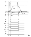
ここで、スタンバイ期間(データの書込み期間及びデータの読み出し期間の経過後)には、参照電位制御回路2が、ビット線対(D、DB)の電位を、参照電位Vrefになるように制御する。図6は、参照電位Vrefと、電源電位VDDとの関係を示すグラフであり、横軸は電源電位VDDを示し、縦軸は電圧を示している。図6には、直線(1)及び直線(2)が示されている。直線(1)及び(2)は、下記式(1)で表される直線である。
(数式1):Vref=a×VDD+b (a<1/2、b>0)
Here, in the standby period (after the data writing period and the data reading period have elapsed), the reference
(Formula 1): Vref = a × VDD + b (a <1/2, b> 0)
ここで、参照電位制御回路2は、参照電位Vrefが、上式(1)で表されるように、ビット線対(D、DB)の電位を制御する。このような高さになるように参照電位Vrefを制御することによって、電源電位VDDが高い場合に参照電位Vrefの値が必要以上に高くなってしまうことが防止される。また、電源電位VDDが低い場合に、参照電位Vrefの値が必要以上に低くなってしまうことを防止できる。すなわち、電源電位VDDの高さが変動した場合におけるセルホールド特性の悪化を防止できる。
Here, the reference
以下に、本発明の実施形態を説明することにより、本発明を詳細に説明する。 Hereinafter, the present invention will be described in detail by describing embodiments of the present invention.
(第1の実施形態)
図7は、本実施形態に係る半導体記憶装置1を示す概略図である。図7に示されるように、本実施形態に係る半導体記憶装置1は、参照電位制御回路2、第1メモリ回路11−1、及び第2メモリ回路11−2を備えている。
(First embodiment)
FIG. 7 is a schematic diagram showing the
本実施形態に係る半導体記憶装置1は、以下の点において、図1に示した半導体記憶装置100とは異なっている。図1に示した半導体記憶装置100においては、各メモリ回路101−1、101−2に、プルダウン回路(105−1、105−2)が設けられている。そして、一方のメモリ回路101−1においてデータの読み出しが行なわれている期間に、他方のメモリ回路101−2において、プルダウン回路105が動作し、ビット線対(D22−DB22)が接地電位GNDにプルダウンされる。これに対して、本実施形態では、プルダウン回路105の代わりに、ダミービット線レベル切替回路17(17−1、17−2)が設けられている。また、参照電位制御回路2には、ダミービット線電位DBLを発生させるダミービット線電位発生回路13が設けられている。そして、一方のメモリ回路(第1メモリ回路11−1)においてデータが読み出されている期間に、他方のメモリ回路(第2メモリ回路11−2)において、ダミービット線レベル切替回路17−2がオンにされ、ビット線対D22−DB22の電位がダミービット線電位DBLになるように制御される。ここで、ダミービット線電位発生回路13は、電源電位VDDに基づいて、ダミービット線電位DBLを決定する。その後、図1に示した半導体記憶装置100と同様に、ビット線対(D11−DB11、D12−DB12、D22−DB22、D21−DB21)間で、チャージシェアが行なわれる。チャージシェア後のビット線対の電位(D11−DB11、D12−DB12、D22−DB22、D21−DB21)は、ビット線対D22−DB22に与えられていたダミービット線電位DBLに依存する。すなわち、ダミービット線電位発生回路13は、ダミービット線電位DBLを制御することにより、チャージシェア後のビット線対電位を制御する。つまり、電源電位VDDに応じて、チャージシェア後のビット線電位を1/2VDD以下の適切な値に設定することができるので、電源電位VDDの高さが変動した場合であっても、セルホールド特性の悪化を防止できる。尚、その他の点については、図1に示した半導体記憶装置100と同様である。
The
以下に、本実施形態に係る半導体記憶装置1を詳細に説明する。
The
参照電位制御回路2は、既述のように、参照電位Vrefを制御する回路である。参照電位制御回路2は、参照電位生成回路12、及びダミービット線電位発生回路13を備えている。参照電位生成回路12は、参照電位配線9に接続されており、参照電位配線9に、参照電位Vrefを供給する機能を有している。尚、チャージシェアした後のビット線は参照電圧生成回路から供給されるVrefによってその電位が設定される。このときの参照電位Vrefは、チャージシェア後のビット線電位と同電位となるように生成される。一方、ダミービット線電位発生回路13は、電源電位VDDの電位に基づいて、ダミービット線電位DBLの電位を決定し、ダミービット線電位DBLを生成する機能を有している。
The reference
次いで、第1メモリ回路11−1の構成を説明する。 Next, the configuration of the first memory circuit 11-1 will be described.
第1メモリ回路11−1は、複数(本実施形態では2つ)のビット線対(D11−DB11、D12−DB12)、セルプレート15−1、及びセンスアンプエリア(14−1、14−2)を備えている。 The first memory circuit 11-1 includes a plurality (two in this embodiment) of bit line pairs (D11-DB11, D12-DB12), a cell plate 15-1, and sense amplifier areas (14-1, 14-2). ).
セルプレート15−1は、複数のメモリセル18(18−1、18−2)を備えている。メモリセル18−1は、キャパシタ3−1及びアクセストランジスタ4−1を備えている。キャパシタ3ー1は、アクセストランジスタ4−1を介して、ビット線D11に接続されている。アクセストランジスタ4−1は、NMOSトランジスタにより実現され、そのゲートは、ワード線WL10に接続されている。一方、メモリセル18−2は、キャパシタ3−2及びアクセストランジスタ4−2を備えている。メモリセル3−2は、アクセストランジスタ4−2を介して、ビット線D12に接続されている。アクセストランジスタ4−2は、NMOSトランジスタにより実現され、そのゲートは、ワード線WL10に接続されている。 The cell plate 15-1 includes a plurality of memory cells 18 (18-1, 18-2). The memory cell 18-1 includes a capacitor 3-1 and an access transistor 4-1. The capacitor 3-1 is connected to the bit line D11 via the access transistor 4-1. The access transistor 4-1 is realized by an NMOS transistor, and its gate is connected to the word line WL10. On the other hand, the memory cell 18-2 includes a capacitor 3-2 and an access transistor 4-2. Memory cell 3-2 is connected to bit line D12 via access transistor 4-2. The access transistor 4-2 is realized by an NMOS transistor, and its gate is connected to the word line WL10.
尚、図示されていないが、セルプレート15−1には、複数のワード線WL10が設けられており、複数のワード線WL10に対応して、複数のメモリセル18が設けられている。選択時(読み出し時又は書き込み時)には、複数のワード線WL10のうちのいずれかが選択され、選択されたワード線WL10に対応するメモリセル18において、キャパシタ3がビット線に接続される。
Although not shown, the cell plate 15-1 is provided with a plurality of word lines WL10, and a plurality of memory cells 18 are provided corresponding to the plurality of word lines WL10. At the time of selection (when reading or writing), one of the plurality of word lines WL10 is selected, and the
センスアンプエリア14−1は、ビット線対(D11−DB11)の電位を制御する部分である。センスアンプエリア14−1には、センスアンプ回路6−1、プリチャージ回路16−1、及びダミービット線レベル切替回路17−1が設けられている。 The sense amplifier area 14-1 is a part that controls the potential of the bit line pair (D11-DB11). In the sense amplifier area 14-1, a sense amplifier circuit 6-1, a precharge circuit 16-1, and a dummy bit line level switching circuit 17-1 are provided.
センスアンプ回路6−1は、ビット線対(D11−DB11)に生じた電位差を増幅する回路である。センスアンプ回路6−1の動作は、制御信号SE11によって制御される。制御信号SE11が活性化され(例えば、ハイレベル)たとき、センスアンプ回路6−1は、ビット線対(D11−DB11)に生じた電位差を増幅する。 The sense amplifier circuit 6-1 is a circuit that amplifies a potential difference generated in the bit line pair (D11-DB11). The operation of the sense amplifier circuit 6-1 is controlled by a control signal SE11. When the control signal SE11 is activated (for example, high level), the sense amplifier circuit 6-1 amplifies the potential difference generated in the bit line pair (D11-DB11).
プリチャージ回路16−1は、ビット線対(D11−DB11)と、参照電位配線9との間の電気的接続を切り替える回路である。プリチャージ回路16−1は、制御信号PDL11により制御される。制御信号PDL11が活性化されたとき、プリチャージ回路16−1は、ビット線対(D11−DB11)を短絡させると共に、参照電位配線9に電気的に接続する。具体的には、プリチャージ回路16−1は、トランジスタTr131、Tr132、及びTr133を備えている。トランジスタTr131は、ビット線D11とビット線DB11間に接続されている。トランジスタTr132は、ビット線D11と参照電位配線9間に接続される。Tr133は、ビット線DB11と参照電位配線9との間に接続されている。トランジスタTr131、Tr132、及びTr133のゲートは、参照電位制御回路2から制御信号PDL11が供給されている。
The precharge circuit 16-1 is a circuit that switches electrical connection between the bit line pair (D 11 -DB 11) and the reference
ダミービット線レベル切替回路17−1は、ビット線対(D11−DB11)と、ダミービット線電位発生回路13との間の電気的接続を切り替える回路である。ダミービット線レベル切替回路17−1は、制御信号PDG11により制御される。制御信号PDG11が活性化されたとき、ダミービット線レベル切替回路17−1は、ビット線対(D11−DB11)を、ダミービット線電位発生回路13に接続する。これにより、ビット線対(D11−DB11)の電位が、ダミービット線電位DBLになるように制御される。具体的には、ダミービット線レベル切替回路17−1は、トランジスタTr151及びTr152を有している。トランジスタTr151は、ビット線D11とダミービット線電位発生回路13間に接続される。Tr152は、ビット線DB11とダミービット線電位発生回路13間に接続されている。トランジスタTr151及びトランジスタTr152のゲートは、参照電位制御回路2から制御信号PDG11が供給されている。
The dummy bit line level switching circuit 17-1 is a circuit that switches electrical connection between the bit line pair (D 11 -DB 11) and the dummy bit line
一方、センスアンプエリア14−2は、ビット線対(D12−DB12)の電位を制御する部分である。センスアンプエリア14−2は、センスアンプエリア14−1と同様に、センスアンプ回路6−2、及びプリチャージ回路16−2を有している。但し、センスアンプエリア4−2に、ダミービット線レベル切替回路17は設けられていない。センスアンプ回路6−2は、ビット線対(D12−DB12)に生じた電位差を増幅するために設けられており、制御信号SE12により制御される。また、プリチャージ回路16−2は、トランジスタTr141、Tr142、Tr143を備えており、制御信号PDL12により制御される。すなわち、制御信号PDL12が活性化されたとき、プリチャージ回路16−2は、ビット線D12とビット線DB12とを短絡させると共に、参照電位配線9に接続する。
On the other hand, the sense amplifier area 14-2 is a part for controlling the potential of the bit line pair (D12-DB12). Similar to the sense amplifier area 14-1, the sense amplifier area 14-2 includes a sense amplifier circuit 6-2 and a precharge circuit 16-2. However, the dummy bit line level switching circuit 17 is not provided in the sense amplifier area 4-2. The sense amplifier circuit 6-2 is provided to amplify the potential difference generated in the bit line pair (D12-DB12), and is controlled by the control signal SE12. The precharge circuit 16-2 includes transistors Tr141, Tr142, and Tr143, and is controlled by a control signal PDL12. That is, when the control signal PDL12 is activated, the precharge circuit 16-2 short-circuits the bit line D12 and the bit line DB12 and connects them to the reference
続いて、第2メモリ回路11−2について説明する。第2メモリ回路11−2も、第1メモリ回路11−1と同様の構成を有している。すなわち、第2メモリ回路11−2は、複数(2つ)のビット線対(D21−DB21、D22−DB22)、セルプレート15−2、及びセンスアンプエリア(14−3、14−4)を有している。 Next, the second memory circuit 11-2 will be described. The second memory circuit 11-2 has the same configuration as the first memory circuit 11-1. That is, the second memory circuit 11-2 includes a plurality (two) of bit line pairs (D21-DB21, D22-DB22), a cell plate 15-2, and sense amplifier areas (14-3, 14-4). Have.
セルアレイプレート15−2には、ワード線WL20、メモリセル(18−3、18−4)が設けられている。各メモリセル(18−3、18−4)は、キャパシタ(3−3、3−4)、及びアクセストランジスタ(4−3、4−4)を有している。 The cell array plate 15-2 is provided with a word line WL20 and memory cells (18-3, 18-4). Each memory cell (18-3, 18-4) has a capacitor (3-3, 3-4) and an access transistor (4-3, 4-4).
センスアンプエリア14−3は、ビット線対(D22−DB22)に対応して設けられており、センスアンプ回路6−3、プリチャージ回路16−3、及びダミービット線レベル切替回路17−2を有している。センスアンプ回路6−3は、制御信号SE22により制御される。プリチャージ回路16−3は、トランジスタTr231、232、233を有しており、制御信号PDL22により制御される。ダミービット線レベル切替回路17−2は、トランジスタTr251、Tr252を有しており、制御信号PDG22により制御される。 The sense amplifier area 14-3 is provided corresponding to the bit line pair (D22-DB22), and includes the sense amplifier circuit 6-3, the precharge circuit 16-3, and the dummy bit line level switching circuit 17-2. Have. The sense amplifier circuit 6-3 is controlled by a control signal SE22. The precharge circuit 16-3 includes transistors Tr231, 232, and 233, and is controlled by a control signal PDL22. The dummy bit line level switching circuit 17-2 includes transistors Tr251 and Tr252 and is controlled by a control signal PDG22.
センスアンプエリア14−4は、ビット線対(D21−DB21)に対応して設けられており、センスアンプ回路6−4、及びプリチャージ回路16−4を有している。センスアンプ回路6−4は、制御信号SE21により制御される。プリチャージ回路16−4は、トランジスタTr241、242、243を有しており、制御信号PDL21により制御される。尚、センスアンプエリア14−4に、ダミービット線レベル切替回路17は設けられていない。 The sense amplifier area 14-4 is provided corresponding to the bit line pair (D21-DB21), and includes a sense amplifier circuit 6-4 and a precharge circuit 16-4. The sense amplifier circuit 6-4 is controlled by a control signal SE21. The precharge circuit 16-4 includes transistors Tr241, 242, and 243, and is controlled by a control signal PDL21. Note that the dummy bit line level switching circuit 17 is not provided in the sense amplifier area 14-4.
続いて、本実施形態に係る半導体記憶装置1の動作方法について説明する。本実施形態においては、第1メモリ回路11−1が選択された場合、第2メモリ回路11−2は非選択になるように制御される。
Subsequently, an operation method of the
図8は、第1メモリ回路11−1においてデータが読み出される場合の動作を示すタイミングチャートである。尚、第1メモリ回路11−1において、メモリセル18−1及びメモリセル18−2には、それぞれ、ハイレベルのデータが格納されているものとする。図8には、ワード線WL10、制御信号SE11/SE12、制御信号PDL11/PDL12、制御信号PDG11、ワード線WL20、制御信号SE12/SE22、制御信号PDL21、制御信号PDL22、及び制御信号PDG22の波形が示されている。また、図9は、各ビット線(D11、D12、D21、D22、DB11、DB12、DB21、DB22)の電位を示すグラフである。 FIG. 8 is a timing chart showing an operation when data is read in the first memory circuit 11-1. In the first memory circuit 11-1, high-level data is stored in each of the memory cell 18-1 and the memory cell 18-2. FIG. 8 shows waveforms of the word line WL10, the control signal SE11 / SE12, the control signal PDL11 / PDL12, the control signal PDG11, the word line WL20, the control signal SE12 / SE22, the control signal PDL21, the control signal PDL22, and the control signal PDG22. It is shown. FIG. 9 is a graph showing the potential of each bit line (D11, D12, D21, D22, DB11, DB12, DB21, DB22).
図8及び図9において、時刻t1以前は、スタンバイ期間である。また、時刻t1からt4までの期間は、第1メモリ回路11−1の読み出し期間である。時刻t4以降は、スタンバイ期間である。 8 and 9, the standby period is before time t1. A period from time t1 to t4 is a reading period of the first memory circuit 11-1. After the time t4, it is a standby period.
時刻t1以前において、参照電位制御回路2は、制御信号PDL11、PDL12、PDL21、及びPDL22として、ハイレベルの信号を供給する。これにより、各メモリ回路11(11−1、11−2)において、プリチャージ回路16(16−1〜16−4)がプリチャージ動作およびイコライジング動作を行なう。その結果、全てのビット線(D11、D12、D21、D22、DB11、DB12、DB21、DB22)は、参照電位配線9に接続される。すなわち、スタンバイ期間において、ビット線(D11、D12、D21、D22、DB11、DB12、DB21、DB22)の電位は、参照電位生成回路12によって生成される参照電位Vrefである。
Prior to time t1, the reference
図8に示されるように、時刻t1において、制御信号PDL11、PDL12がローレベルに切り替えられる。また、制御信号PDL22も、ローレベルに切り替えられる。これにより、選択された第1メモリ回路11−1において、ビット線対D11−DB11、D12−DB12のプリチャージ状態が解除される。また、非選択の第2メモリ回路11−2においては、ビット線対D22−DB22のプリチャージ状態が解除される。但し、ビット線対D21−DB21については、制御信号PDL21が変化せず、プリチャージ状態が維持されている。 As shown in FIG. 8, at time t1, the control signals PDL11 and PDL12 are switched to a low level. The control signal PDL22 is also switched to a low level. As a result, in the selected first memory circuit 11-1, the precharge state of the bit line pair D11-DB11, D12-DB12 is released. In the non-selected second memory circuit 11-2, the precharge state of the bit line pair D22-DB22 is released. However, for the bit line pair D21-DB21, the control signal PDL21 does not change and the precharge state is maintained.
続く時刻t2に、第1メモリ回路11−1においてワード線WL10が選択される。すなわち、ワード線WL10にハイレベルの信号が供給される。これにより、第1メモリ回路11−1においては、キャパシタ3−1がビット線D11と電気的に接続され、キャパシタ3−2がビット線D12と電気的に接続される。既述のように、キャパシタ3−1及びキャパシタ3−2には、それぞれ、ハイレベルのデータが格納されている。そのため、図9に示されるように、ビット線D11及びD12の電位は、参照電位Vrefから僅かに上昇する。 At subsequent time t2, the word line WL10 is selected in the first memory circuit 11-1. That is, a high level signal is supplied to the word line WL10. Thereby, in the first memory circuit 11-1, the capacitor 3-1 is electrically connected to the bit line D11, and the capacitor 3-2 is electrically connected to the bit line D12. As described above, high-level data is stored in each of the capacitor 3-1 and the capacitor 3-2. Therefore, as shown in FIG. 9, the potentials of the bit lines D11 and D12 slightly increase from the reference potential Vref.
一方、時刻t2においては、図8に示されるように、制御信号PDG22がハイレベルに切り替えられる。その結果、第2メモリ回路11−2において、ダミービット線レベル切替回路17−2により、ビット線対D22−DB22がダミービット線電位発生回路13と電気的に接続される。その結果、図9に示されるように、ビット線対D22−DB22の電位は、ダミービット線電位DBLになるように、変化する。
On the other hand, at time t2, as shown in FIG. 8, the control signal PDG22 is switched to the high level. As a result, in the second memory circuit 11-2, the bit line pair D22-DB22 is electrically connected to the dummy bit line
その後、図8に示されるように、時刻t3において、制御信号SE11及びSE12がハイレベルに切り替えられる。その結果、第1メモリ回路11−1において、センスアンプ回路6(6−1、6−2)が活性化する。すなわち、センスアンプ回路6−1がビット線対D11−DB11の電位差を増幅し、センスアンプ回路6−2がビット線対D12−DB12の電位差を増幅する。その結果、図9に示されるように、ビット線D11及びD12の電位は、電源電位VDDにまで引き上げられ、ビット線DB11及びDB12の電位は、接地電位GNDになるように引き下げられる。そして、増幅された電位差が、データバス(図示せず)を介して読み出される。 Thereafter, as shown in FIG. 8, at time t3, the control signals SE11 and SE12 are switched to the high level. As a result, the sense amplifier circuit 6 (6-1, 6-2) is activated in the first memory circuit 11-1. That is, the sense amplifier circuit 6-1 amplifies the potential difference between the bit line pair D11-DB11, and the sense amplifier circuit 6-2 amplifies the potential difference between the bit line pair D12-DB12. As a result, as shown in FIG. 9, the potentials of the bit lines D11 and D12 are raised to the power supply potential VDD, and the potentials of the bit lines DB11 and DB12 are lowered to the ground potential GND. The amplified potential difference is read out via a data bus (not shown).
その後、図8に示されるように、時刻t4において、ワード線WL10に供給される信号、制御信号SE11、SE12、及び制御信号PDG22が、ローレベルに切り替えられる。また、続く時刻t5において、制御信号PDL11、PDL12、及びPDL22が、ハイレベルに切り替えられる。プリチャージ回路16−1、16−2、16−3がプリチャージ動作及びイコライジング動作を行なう。その結果、ビット線対D11−DB11、D12−DB12、D22−DB22が、参照電位配線9を介して電気的に接続される。よって、ビット線D11−DB11、D12−DB12、D22−DB22間においてチャージシェアが行なわれ、ビット線D11−DB11、D12−DB12、D22−DB22の電位は、平均化される。このときは、たとえば、1/3VDD+1/3DBL(DBL:ダミービット線電位)になる。尚、ビット線(D21−DB21)は、チャージシェア前から参照電位Vrefであるので、電荷シェアには影響しない。このため、参照電位生成回路から供給される参照電位Vrefを、上記チャージシェアを行なった結果の電位に設定しておくことで、ビット線(D21−DB21)は上述したチャージシェアにほとんど関係せず、電位の変化も起こらない。
Thereafter, as shown in FIG. 8, at time t4, the signals supplied to the word line WL10, the control signals SE11 and SE12, and the control signal PDG22 are switched to the low level. At subsequent time t5, the control signals PDL11, PDL12, and PDL22 are switched to the high level. Precharge circuits 16-1, 16-2 and 16-3 perform a precharge operation and an equalizing operation. As a result, the bit line pairs D11-DB11, D12-DB12, D22-DB22 are electrically connected through the reference
上述のように、チャージシェア後のビット線対の電位は、チャージシェア前におけるビット線対(D11−DB11、D12−DB12、D22−DB22)の電位によって、決められる。従って、チャージシェア後のビット線対の電位は、ビット線対(D22−DB22)の電位であるダミービット線電位DBLの電位によって決まる。ここで、本実施形態においては、ダミービット線電位発生回路13(図7参照)が、電源電位VDDの高さに基づいて、ダミービット線電位DBLの電位を可変にすることによって、チャージシェア後のビット線対の電位を適切な高さに設定することが可能となる。 As described above, the potential of the bit line pair after charge sharing is determined by the potential of the bit line pair (D11-DB11, D12-DB12, D22-DB22) before charge sharing. Therefore, the potential of the bit line pair after charge sharing is determined by the potential of the dummy bit line potential DBL that is the potential of the bit line pair (D22-DB22). Here, in the present embodiment, the dummy bit line potential generation circuit 13 (see FIG. 7) changes the potential of the dummy bit line potential DBL based on the height of the power supply potential VDD, so that after charge sharing. It is possible to set the potential of the bit line pair to an appropriate height.
図10は、電源電位VDD、ダミービット線電位DBL、及び参照電位Vrefの関係を示すグラフである。図10に示されるように、ダミービット線電位発生回路13は、電源電位VDDが低いときにダミービット線電位DBLが高くなり、電源電位VDDが高いときにダミービット線電位DBLが低くなるように、ダミービット線電位DBLの電位を決定する。
FIG. 10 is a graph showing the relationship between the power supply potential VDD, the dummy bit line potential DBL, and the reference potential Vref. As shown in FIG. 10, the dummy bit line
このように、電源電位VDDが高くなった場合には、参照電位Vrefを1/2VDDに比べて十分に低い電圧に設定することができる。一方、電源電位VDDが低くなった場合には、参照電位Vrefを1/2VDDに近い電圧に設定することができる。したがって、電源電位VDDが低下した場合であっても、参照電位Vrefが必要以上に低くならず、ロウレベルデータを読み出す場合であっても、センスアンプの読み出しマージンを確保することができる。また、ダミービット線電位DBLを、1/2VDDよりは低いが接地電位GNDよりも高い電位にすることで、ダミービット線電位DBLが与えられるビット線対に接続されるメモリセルのデジットディスターブホールド(DDH)特性の悪化を防ぐこともできる。なお、従来技術と同様に、1/2VDDよりも低電位でビット線をプリチャージしているため、メモリセルのハイレベルデータのホールド特性を改善する効果は変わらない。さらに、ダミービット線電位を供給する動作を、データ読み出し期間に行ない、チャージシェアを行なっているため、回路動作の高速化する効果も維持される。 As described above, when the power supply potential VDD becomes high, the reference potential Vref can be set to a voltage sufficiently lower than ½ VDD. On the other hand, when the power supply potential VDD becomes low, the reference potential Vref can be set to a voltage close to ½ VDD. Therefore, even when the power supply potential VDD is lowered, the reference potential Vref is not lowered more than necessary, and a read margin of the sense amplifier can be ensured even when low level data is read. Further, by setting the dummy bit line potential DBL to a potential lower than ½ VDD but higher than the ground potential GND, the digit disturb hold of the memory cell connected to the bit line pair to which the dummy bit line potential DBL is applied ( DDH) characteristics can also be prevented from deteriorating. As in the prior art, since the bit line is precharged at a potential lower than ½ VDD, the effect of improving the high-level data hold characteristic of the memory cell remains the same. Further, since the dummy bit line potential is supplied during the data read period and charge sharing is performed, the effect of increasing the circuit operation speed is also maintained.
尚、本実施形態においては、第1メモリ回路11−1における複数(2つ)のビット線対(D11−DB11、D12−DB12)と、第2メモリ回路11−2における複数(2つ)のビット線対(D21−DB21、D22−DB22)との間でチャージシェアが行なわれる場合について説明した。但し、必ずしも、これらのビット線対(D11−DB11、D12−DB12、D21−DB21、D22−DB22)間でチャージシェアが行なわれる必要はない。例えば、一方のメモリ回路11−1における1つのビット線対と、他方のメモリ回路11−2における1つのビット線対との間でチャージシェアが行われてもよい。また、チャージシェア時に、各ビット線対のうちの一方のビット線だけが参照電位配線9に接続されてもよい。参照電位配線9に接続されるビット線の本数を調整することにより、参照電位Vrefの高さを制御することも可能である。
In the present embodiment, a plurality (two) of bit line pairs (D11-DB11, D12-DB12) in the first memory circuit 11-1 and a plurality (two) of the second memory circuit 11-2. The case where charge sharing is performed with the bit line pair (D21-DB21, D22-DB22) has been described. However, it is not always necessary to perform charge sharing between these bit line pairs (D11-DB11, D12-DB12, D21-DB21, D22-DB22). For example, charge sharing may be performed between one bit line pair in one memory circuit 11-1 and one bit line pair in the other memory circuit 11-2. Further, only one bit line of each bit line pair may be connected to the reference
また、本実施形態においては、ダミービット線電位発生回路13が、電源電位VDDの高さに基づいて、ダミービット線電位DBLの高さを決定する場合について説明した。ここで、高温時には、メモリセルからのオフリークも増大する。そのため、高温時には、参照電位Vrefを低く設定することが望まれる。そこで、ダミービット線電位発生回路13は、更に、温度に基づいて、ダミービット線電位DBLの高さを決定することが好ましい。具体的には、ダミービット線電位発生回路13は、図示しない温度センサによる温度の測定結果に基づいて、高温時に、ダミービット線電位DBLが低くなり、低温時にダミービット線電位DBLが高くなるように、ダミービット線電位DBLの高さを決定することが好ましい。これにより、高温時に参照電位Vrefを下げることが可能となり、メモリセルホールド特性を改善することができる。
In the present embodiment, the case where the dummy bit line
また、本実施形態においては、データが読み出された場合の動作について説明した。但し、データが書き込まれた場合においても、時刻t4以降と同様の動作を行うことにより、参照電位Vrefの高さを制御することが可能である。 In this embodiment, the operation when data is read has been described. However, even when data is written, the height of the reference potential Vref can be controlled by performing an operation similar to that after time t4.
(第2の実施形態)
続いて、第2の実施形態について説明する。図11は、本実施形態に係る半導体記憶装置1を示す概略図である。尚、図11には、第1メモリ回路11−1、第2メモリ回路11−2、及び参照電位制御回路2が示されている。また、本実施形態においては、第1の実施形態とは異なり、参照電位制御回路2にダミービット線電位発生回路13は設けられていない。
(Second Embodiment)
Next, the second embodiment will be described. FIG. 11 is a schematic diagram showing the
まず、第1メモリ回路11−1の構成を説明する。第1メモリ回路11−1には、一対のビット線対D1−DB1、セルプレート15−1、センスアンプエリア14−5、及びYスイッチ回路YSW1が設けられている。 First, the configuration of the first memory circuit 11-1 will be described. In the first memory circuit 11-1, a pair of bit lines D1-DB1, a cell plate 15-1, a sense amplifier area 14-5, and a Y switch circuit YSW1 are provided.
セルプレート15−1には、複数のキャパシタ3、及び複数のアクセストランジスタ4が設けられている。各キャパシタ3は、各アクセストランジスタ4を介して、ビット線対(D1−DB1)の一方に接続されている。各アクセストランジスタ4は、複数のワード線WL1のうちの何れかにより制御され、対応するワード線WL1が選択された場合に、各キャパシタ3をビット線対(D1−DB1)の一方に接続する。複数のワード線WL1は、ワード線ドライバ5によって選択される。
The cell plate 15-1 is provided with a plurality of
センスアンプエリア14−5には、センスアンプ回路6、イコライザ回路19、及びプリチャージ回路16が設けられている。
In the sense amplifier area 14-5, a
センスアンプ回路6は、PMOSトランジスタT1、T2、及びNMOSトランジスタT3、T4を備えている。PMOSトランジスタT1、T2の共通ソースは、制御信号SP1が供給されるように、参照電位制御回路2に接続されている。NMOSトランジスタT3、T4の共通ソースは、制御信号SN1が供給されるように、参照電位制御回路2に接続されている。このセンスアンプ回路6は、制御信号SP1としてハイレベルの信号が供給され、制御信号SN1としてローレベルの信号が供給されたときに、ビット線対(D1−DB1)の電位差を増幅する。
The
イコライザ回路19は、ビット線対(D1−DB1)を短絡させるために設けられている。イコライザ回路19は、制御信号EQ1によって制御され、制御信号EQ1がオン(ハイレベル)のときに、ビット線対(D1−DB1)を短絡する。
The
プリチャージ回路16は、ビット線対(D1−DB1)を、参照電位配線9に接続する為に設けられている。プリチャージ回路16は、トランジスタT5、T6を備えている。トランジスタT5、T6は、ビット線D1とビット線DB1との間に直列に接続されている。トランジスタT5とトランジスタT6との間の接続点は、参照電位配線9に接続されている。トランジスタT5及びT6のゲートは、制御信号PDL1が供給されるように、参照電位制御回路2(図示せず)に接続されている。
The
また、ビット線対(D1−DB1)は、Yスイッチ回路YSW1を介して、データバス線21に接続されている。読み出し時又は書込み時には、Yスイッチ回路YSW1がオンにされ、データバス線21を介してデータの読み出し又は書込みが行なわれる。
The bit line pair (D1-DB1) is connected to the
続いて、第2メモリ回路11−2の構成を説明する。第2メモリ回路11−2も、第1メモリ回路11−1と同様の構成を有している。すなわち、第2メモリ回路11−2は、ビット線対(D2−DB2)、セルプレート15−2、センスアンプエリア14−6を有している。 Next, the configuration of the second memory circuit 11-2 will be described. The second memory circuit 11-2 has the same configuration as the first memory circuit 11-1. That is, the second memory circuit 11-2 includes a bit line pair (D2-DB2), a cell plate 15-2, and a sense amplifier area 14-6.
セルプレート15−2には、複数のキャパシタ3及び複数のアクセストランジスタ4が設けられており、各キャパシタ3は、各アクセストランジスタ4を介してビット線対(D2−DB2)の一方に接続されている。複数のアクセストランジスタ4は、複数のワード線WL2によって制御される。
The cell plate 15-2 is provided with a plurality of
センスアンプエリア14−6には、センスアンプ回路6、イコライザ回路19、及びプリチャージ回路16が設けられている。センスアンプ回路6において、PMOSトランジスタT1、T2の共通ソースは、制御信号SP2が供給されるように、参照電位制御回路2に接続されている。また、NMOSトランジスタT3、T4の共通ソースは、制御信号SN2が供給されるように、参照電位制御回路2に接続されている。イコライザ回路19は、制御信号EQ2によって制御され、制御信号EQ2がオン(ハイレベルのときに)、ビット線対(D2−DB2)を短絡させる。プリチャージ回路16は、トランジスタT5及びT6を有しており、制御信号PDL2によって制御される。プリチャージ回路16は、制御信号PDL2がオンのとき、ビット線対(D2−DB2)を参照電位配線9に接続する。
In the sense amplifier area 14-6, a
また、本実施形態において、制御信号SP1、SN1、EQ1、PDL1、SP2、SN2、EQ2、及びPDL2は、参照電位制御回路2によって供給される。
In this embodiment, the control signals SP1, SN1, EQ1, PDL1, SP2, SN2, EQ2, and PDL2 are supplied by the reference
続いて、本実施形態に係る半導体記憶装置1の動作方法を説明する。図12は、本実施形態に係る半導体記憶装置1の動作方法を示すタイミング図である。図12には、第1メモリ回路11−1からデータが読み出されるときの動作が示されている。図12には、ビット線D1、DB1、D2、及びDB2の電位が示されている。また、図12には、制御信号SP1、SN1、PDL1、EQ1、SN2、及びPDL2の波形が示されている。尚、制御信号EQ2はハイレベルに固定され、制御信号SP2はローレベルに固定される。
Subsequently, an operation method of the
図12において、時刻t1以前は、スタンバイ期間である。スタンバイ期間においては、制御信号SP1、SP2としてローレベルの信号が供給され、制御信号SN1、PDL1、EQ1、SN2、EQ2及びPDL2としては、ハイレベルの信号が供給される。すなわち、スタンバイ期間においては、各メモリ回路11のセンスアンプ回路6は動作していない。また、各メモリ回路において、イコライザ回路19によりビット線対(D1−DB1、D2−DB2)が短絡されている。また、各メモリ回路のビット線対(D1−DB1、D2−DB2)は、プリチャージ回路16により、参照電位配線9に接続されている。すなわち、各メモリ回路11におけるビット線対(D1−DB1、D2−DB2)の電位は、参照電位Vrefになっている。
In FIG. 12, the standby period is before time t1. In the standby period, low level signals are supplied as the control signals SP1, SP2, and high level signals are supplied as the control signals SN1, PDL1, EQ1, SN2, EQ2, and PDL2. That is, the
時刻t1において、制御信号PDL1、EQ1、及びPDL2がローレベルに切り替えられる。また、ワード線WL1の電位が、アクセストランジスタ4を確実にオンにする為に、電源電位VDDよりも高いVPPにまで引き上げられる。制御信号PDL1及びEQ1がローレベルに切り替えられることにより、第1メモリ回路11−1では、ビット線対(D1−DB1)が、参照電位配線9から遮断される。また、ビット線D1とDB1との間も電気的に遮断される。そして、ワード線WL1が選択されることにより、キャパシタ3がビット線D1と接続される。ここで、キャパシタ3にハイレベルのデータが格納されている場合には、ビット線D1の電位が、参照電位Vrefから僅かに上昇する。一方、制御信号PDL2がローレベルに切り替えられることにより、第2メモリ回路11−2においては、ビット線対(D2−DB2)が参照電位配線9から遮断される。ただし、制御信号EQ2にはハイレベルの信号の供給が維持されているため、ビット線対D2−DB2間は短絡している。
At time t1, the control signals PDL1, EQ1, and PDL2 are switched to a low level. Further, the potential of the word line WL1 is raised to VPP higher than the power supply potential VDD in order to reliably turn on the
その後、時刻t2において、制御信号SP1がハイレベルに切り替えられ、制御信号SN1がローレベルに切り替えられ、制御信号SN2がローレベルに切り替えられる。これにより、第1メモリ回路11−1においては、センスアンプ回路6が駆動し、ビット線対(D1−DB1)に生じた電位差を増幅する。すなわち、ビット線D1の電位が電源電位VDDにまで引き上げられ、ビット線DB1の電位が接地電位GNDに引き下げられる。
Thereafter, at time t2, the control signal SP1 is switched to high level, the control signal SN1 is switched to low level, and the control signal SN2 is switched to low level. Thereby, in the first memory circuit 11-1, the
一方、第2メモリ回路11−2からはデータが読み出されないので、制御信号SP2としてローレベルの信号の供給が維持されているが、制御信号SN2には、時刻t2において、ローレベルの信号が供給される。その結果、ビット線対(D2、DB2)の電位が、トランジスタT3及びT4の閾値電圧VTNになるように変化する。以下に、この点について説明する。 On the other hand, since data is not read from the second memory circuit 11-2, supply of a low level signal as the control signal SP2 is maintained. However, at time t2, the low level signal is supplied to the control signal SN2. Supplied. As a result, the potential of the bit line pair (D2, DB2) changes so as to become the threshold voltage VTN of the transistors T3 and T4. This point will be described below.
図13は、制御信号SP2及びSN2としてそれぞれローレベルの信号が供給された場合における、センスアンプ回路6の等価回路を示す図である。図13に示されるように、制御信号SP2及びSN2がローレベルである場合には、PMOSトランジスタT1及びT2はオフ状態になる。その結果、センスアンプ回路6においては、NMOSトランジスタT3及びT4が、接地電位(制御信号SN2=ローレベル)とビット線対(D2−DB2)との間にダイオード接続される。ここで、ビット線対(D2−DB2)は、イコライザ回路19により短絡されているので、ビット線対(D2−DB2)の電位は、NMOSトランジスタT3及びT4の閾値電圧VTNになるように、変化する。
FIG. 13 is a diagram showing an equivalent circuit of the
その後、図12に示されるように、時刻t3において、ワード線WL1の電位がローレベルに引き下げられる。また、制御信号SP1がローレベルに切り替えられ、制御信号SN1、PDL1、EQ1、SN2,及びPDL2がハイレベルに切り替えられる。その結果、既述の実施形態と同様に、第1メモリ回路11−2におけるビット線対(D1−DB1)と、第2メモリ回路11−2におけるビット線対(D2−DB2)とが、参照電位配線9を介して互いに接続される。既述の実施形態と同様に、ビット線(D1、DB1、D2、DB2)間でチャージシェアが行なわれる。
Thereafter, as shown in FIG. 12, at time t3, the potential of the word line WL1 is lowered to the low level. Further, the control signal SP1 is switched to a low level, and the control signals SN1, PDL1, EQ1, SN2, and PDL2 are switched to a high level. As a result, as in the above-described embodiment, the bit line pair (D1-DB1) in the first memory circuit 11-2 and the bit line pair (D2-DB2) in the second memory circuit 11-2 are referred to. They are connected to each other through a
本実施形態においては、選択されたメモリ回路(第1メモリ回路11−1)においてデータの読み出しが行なわれている間に、非選択のメモリ回路(第2メモリ回路11−2)のビット線対(D2−DB2)の電位(以下、ダミービット線レベルDBL)が、NMOSトランジスタ(T3、T4)の閾値電圧VTNになるように制御される。すなわち、ダミービット線レベルDBLは、閾値電圧VTNである。これにより、既述の実施形態と同様の効果が得られる。 In the present embodiment, the bit line pair of the non-selected memory circuit (second memory circuit 11-2) is read while data is being read in the selected memory circuit (first memory circuit 11-1). The potential of (D2-DB2) (hereinafter, dummy bit line level DBL) is controlled to be the threshold voltage VTN of the NMOS transistors (T3, T4). That is, the dummy bit line level DBL is the threshold voltage VTN. Thereby, the same effect as the above-described embodiment can be obtained.
また、NMOSトランジスタ(T3、T4)の閾値電圧VTNは、温度に応じて依存する。すなわち、高温時には、閾値電圧VTNが低下し、ダミービット線レベルDBLも低くなる。その結果、参照電位Vrefの高さを、温度に応じて適切に制御することができる。図14は、電源電位VDD、ダミービット線レベル(DBL−1、DBL−2)、及び参照電位(Vref−1、Vref−2)の関係を示すグラフである。尚、ダミービット線レベルDBL−1及び参照電位Vref−1は、それぞれ、高温時におけるダミービット線レベルDBL及び参照電位Vrefを示す。ダミービット線レベルDBL−2及び参照電位Vref−2は、それぞれ、低温時におけるダミービット線レベルDBL及び参照電位Vrefを示す。図14に示されるように、高温時には、低温時よりも、NMOSトランジスタ(T3、T4)の閾値電圧VTNが低下する。その結果、高温時におけるダミービット線レベルDBL−1は、低温時におけるダミービット線レベルDBL−2よりも、低くなる。その結果、高温時における参照電位Vref−1も、低温時における参照電位Vref−2よりも、低くなる。既述のように、高温時には、メモリセルからのオフリークも増大する。そのため、高温時には、参照電位Vrefを低い値に設定することが望まれる。本実施形態によれば、ダミービット線レベルDBLが、NMOSトランジスタ(T3、T4)の閾値電圧VTNになるように制御されるので、高温時には、参照電位Vrefを低い電位になるように制御することができ、セルホールド特性を改善することができる。 The threshold voltage VTN of the NMOS transistors (T3, T4) depends on the temperature. That is, at a high temperature, the threshold voltage VTN decreases and the dummy bit line level DBL also decreases. As a result, the height of the reference potential Vref can be appropriately controlled according to the temperature. FIG. 14 is a graph showing the relationship among the power supply potential VDD, the dummy bit line levels (DBL-1, DBL-2), and the reference potentials (Vref-1, Vref-2). The dummy bit line level DBL-1 and the reference potential Vref-1 indicate the dummy bit line level DBL and the reference potential Vref at high temperatures, respectively. The dummy bit line level DBL-2 and the reference potential Vref-2 indicate the dummy bit line level DBL and the reference potential Vref at low temperatures, respectively. As shown in FIG. 14, at the high temperature, the threshold voltage VTN of the NMOS transistors (T3, T4) is lower than at the low temperature. As a result, the dummy bit line level DBL-1 at a high temperature is lower than the dummy bit line level DBL-2 at a low temperature. As a result, the reference potential Vref-1 at high temperature is also lower than the reference potential Vref-2 at low temperature. As described above, the off-leak from the memory cell also increases at a high temperature. Therefore, it is desirable to set the reference potential Vref to a low value at high temperatures. According to the present embodiment, since the dummy bit line level DBL is controlled to be the threshold voltage VTN of the NMOS transistors (T3, T4), the reference potential Vref is controlled to be a low potential at a high temperature. And cell hold characteristics can be improved.
また、本実施形態によれば、第1の実施形態とは異なり、ダミービット線レベルDBLを制御するために、参照電位制御回路2にダミービット線電位発生回路13(図7参照)が設けられている必要がない。また、各メモリ回路11に、ダミービット線レベル切替回路17(図7参照)が設けられている必要がない。従って、第1の実施形態と比べて、回路構成を簡単にすることが可能である。
Further, according to the present embodiment, unlike the first embodiment, a dummy bit line potential generation circuit 13 (see FIG. 7) is provided in the reference
また、本実施形態では、第1メモリ回路11−1及び第2メモリ回路11−2の配置を工夫することにより、回路構成を更に簡単にすることができる。図15は、第1メモリ回路11−1及び第2メモリ回路11−2の配置の一例を示す概略図である。図15に示される例においては、第1メモリ回路11−1と第2メモリ回路11−2とが隣接して配置されている。そして、第1メモリ回路11−1においては、セルプレート15−1よりも第2メモリ回路11−2側に、センスアンプエリア14−5が配置されている。一方、第2メモリ回路11−2においては、セルプレート15−2よりも第1メモリ回路11−1側に、センスアンプエリア14−6が配置されている。すなわち、第1メモリ回路11−1及び第2メモリ回路11−2は、センスアンプエリア14同士で隣接するように配置されている。
In the present embodiment, the circuit configuration can be further simplified by devising the arrangement of the first memory circuit 11-1 and the second memory circuit 11-2. FIG. 15 is a schematic diagram illustrating an example of the arrangement of the first memory circuit 11-1 and the second memory circuit 11-2. In the example shown in FIG. 15, the first memory circuit 11-1 and the second memory circuit 11-2 are arranged adjacent to each other. In the first memory circuit 11-1, the sense amplifier area 14-5 is arranged closer to the second memory circuit 11-2 than the cell plate 15-1. On the other hand, in the second memory circuit 11-2, the sense amplifier area 14-6 is arranged closer to the first memory circuit 11-1 than the cell plate 15-2. That is, the first memory circuit 11-1 and the second memory circuit 11-2 are arranged adjacent to each other in the
ここで、図12にされるように、制御信号SN1及び制御信号SN2は、常に同じレベルの信号である。また、制御信号PDL2及びPDL1も、同じレベルの信号である。従って、センスアンプエリア14同士が隣接するように第1メモリ回路11−1及び第2メモリ回路11−2を配置すれば、共通の配線を介して、センスアンプエリア14−5に制御信号SN1を供給し、センスアンプエリア14−6に制御信号SN2を供給することができる。同様に、共通の配線を用いて、センスアンプエリア14−5に制御信号PDL1を供給し、センスアンプエリア14−6に制御信号PDL2を供給することができる。これより、制御信号に要する配線を少なくすることができ、回路構成を簡単にすることが可能である。
Here, as shown in FIG. 12, the control signal SN1 and the control signal SN2 are always signals of the same level. The control signals PDL2 and PDL1 are also the same level signals. Therefore, if the first memory circuit 11-1 and the second memory circuit 11-2 are arranged so that the
(第3の実施形態)
続いて、第3の実施形態について説明する。既述の実施形態においては、第1のメモリ回路11−1のビット線対と、第2のメモリ回路11−2のビット線対との間でチャージシェアを行うことにより、参照電位Vrefのレベルが決定される。これに対して、本実施形態においては、単一のメモリ回路において、参照電位Vrefのレベルが決定される。
(Third embodiment)
Subsequently, a third embodiment will be described. In the embodiment described above, the level of the reference potential Vref is obtained by performing charge sharing between the bit line pair of the first memory circuit 11-1 and the bit line pair of the second memory circuit 11-2. Is determined. On the other hand, in the present embodiment, the level of the reference potential Vref is determined in a single memory circuit.
図16は、本実施形態に係る半導体記憶装置1におけるメモリ回路11の構成を示す概略図である。本実施形態におけるメモリ回路11は、第2の実施形態における各メモリ回路11(11−1、11−2)と同様の構成を有している。すなわち、このメモリ回路11は、複数のキャパシタ3、一対のビット線(D−DB)、セルプレート15、及びセンスアンプエリア14を有している。複数のキャパシタ3の各々は、アクセストランジスタ4を介して、ビット線対(D−DB)の一方に接続されている。また、アクセストランジスタ4は、対応するワード線が選択されたときにオンになる。一方、センスアンプエリア14には、センスアンプ回路6、イコライザ回路19、及びプリチャージ回路16が設けられている。センスアンプ回路6は、制御信号SP及びSNによって制御される。イコライザ回路19は、制御信号EQによって制御され、ビット線対(D−DB)を短絡させる。プリチャージ回路16は、制御信号PDLによって制御され、ビット線対(D−DB)を参照電位配線9に接続する。また、ビット線対(D−DB)は、スイッチ回路YSWを介して、データバス線21に接続されている。
FIG. 16 is a schematic diagram showing the configuration of the
尚、制御信号SP、SN、PDL、及びEQは、参照電位制御回路2によって供給される。
The control signals SP, SN, PDL, and EQ are supplied by the reference
図17は、半導体記憶装置1の動作方法を示すタイミングチャートである。図17には、ビット線対(D−DB)の波形、及び、制御信号SP、SN、PDL、及びEQの波形が示されている。図17において、時刻t1以前は、スタンバイ期間である。また、時刻t1から時刻t3までの期間は、読み出し期間(センス動作期間)である。時刻t3から時刻t4までの期間は、プリチャージ期間である。時刻t4以降は、スタンバイ期間である。
FIG. 17 is a timing chart showing an operation method of the
時刻t1以前においては、制御信号SPとしてローレベルの信号が供給され、制御信号SN、PDL,及びEQとしてそれぞれハイレベルの信号が供給される。このとき、ビット線対(D−DB)は、短絡されると共に、参照電位配線9に接続される。すなわち、ビット線対(D−DB)の電位は、参照電位Vrefになるように制御される。
Prior to time t1, a low level signal is supplied as the control signal SP, and a high level signal is supplied as the control signals SN, PDL, and EQ. At this time, the bit line pair (D-DB) is short-circuited and connected to the reference
時刻t1において、ワード線WL1が選択され、制御信号PDL及びEQがローレベルに変更される。制御信号PDL及びEQがローレベルになることにより、ビット線対(D−DB)は、参照電位配線9から切り離される。また、ビット線対(D−DB)は、互いに遮断される。そして、ワード線WL1が選択されることにより、キャパシタ3がビット線Dに接続される。キャパシタ3にハイレベルのデータが格納されている場合には、ビット線Dの電位が参照電位Vrefから僅かに上昇する。
At time t1, the word line WL1 is selected, and the control signals PDL and EQ are changed to a low level. When the control signals PDL and EQ become low level, the bit line pair (D-DB) is disconnected from the reference
その後、時刻t2において、制御信号SPがハイレベルに切り替えられ、制御信号SNがローレベルに切り替えられる。これにより、センスアンプ回路6が動作し、ビット線対(D−DB)に生じた電位差が増幅される。すなわち、ビット線Dの電位が電源電位VDDにまで引き上げられ、ビット線DBの電位が接地電位GNDにまで引き下げられる。
Thereafter, at time t2, the control signal SP is switched to the high level, and the control signal SN is switched to the low level. As a result, the
その後、時刻t3において、ワード線WL1の電位が接地電位に引き下げられ、制御信号SPがローレベルに切り替えられ、制御信号EQがハイレベルに切り替えられる。これにより、第2の実施形態と同様に、センスアンプ回路6では、NMOSトランジスタ(T3、T4)が、ビット線対(D−DB)と接地電位GNDとの間にダイオード接続されることになる。その結果、ビット線対(D−DB)の電位は、一旦1/2VDDに近づいた後、NMOSトランジスタT3及びT4の閾値電圧VTNに向かって降下する。
Thereafter, at time t3, the potential of the word line WL1 is lowered to the ground potential, the control signal SP is switched to the low level, and the control signal EQ is switched to the high level. As a result, as in the second embodiment, in the
その後、時刻t4において、制御信号SN及びPDLがハイレベルに切り替えられる。これにより、ビット線対(D−DB)が参照電位配線9に接続され、ビット線対(D−DB)の電位が参照電位Vrefに固定される。ここで、プリチャージ期間(時刻t3からt4までの期間)が長く設定された場合には、参照電位Vrefが低くなり(閾値電圧VTNに近くなり)、プリチャージ期間が短く設定された場合には、参照電位Vrefが高くなる。従って、参照電位制御回路2に遅延回路などを設け、プリチャージ期間の長さを制御することにより、参照電位Vrefの高さを適切な高さに設定することができる。参照電位制御回路2から供給される参照電位Vrefの設定も同様に調整すればよい。
Thereafter, at time t4, the control signals SN and PDL are switched to the high level. Thereby, the bit line pair (D-DB) is connected to the reference
本実施形態によれば、センス動作期間の後に、プリチャージ期間を設けなければならないが、参照電位制御回路2に、ダミービット線電位発生回路13(図7参照)を設けることなく、参照電位Vrefを適切な高さに設定することが可能である。従って、電源電位VDDが変動した場合であっても、読み出しマージンの悪化を防止できる。
According to the present embodiment, a precharge period must be provided after the sense operation period, but the reference potential Vref is not provided in the reference
また、参照電位Vrefの高さが閾値電圧VTNになるように制御される場合には、参照電位Vrefを参照電位配線9に供給する参照電位生成回路12として、NMOSトランジスタ(T3、T4)と同一のサイズのNMOSトランジスタが用いられることが好ましい。このようなMMOSトランジスタを用いることにより、参照電位配線9に供給される参照電位Vrefの高さを、NMOSトランジスタ(T3、T4)の閾値電圧VTNに正確に一致させることができる。
Further, when the reference potential Vref is controlled to have a threshold voltage VTN, the reference
以上、本発明について、第1乃至第3の実施形態を用いて説明した。尚、これらの実施形態は互いに独立するものではなく、矛盾のない範囲内で組み合わせて用いることも可能である。 The present invention has been described above using the first to third embodiments. These embodiments are not independent from each other, and can be used in combination within a consistent range.
1 半導体記憶装置
2 参照電位制御回路
3 キャパシタ
4 アクセストランジスタ
5 ワード線ドライバ
6 センスアンプ回路
7 データバス
9 参照電位配線
10 ワードドライバ
11(11−1〜11−2) メモリ回路
12 参照電位生成回路
13 ダミービット線電位発生回路
14(14−1〜14−6) センスアンプエリア
15(15−1、15−2) セルプレート
16(16−1〜16−4) プリチャージ回路
17(17−1、17−2) ダミービット線レベル切替回路
18(18−1〜18−4) メモリセル
19 イコライザ回路
20 データバス線スイッチ
21 データバス線
100 半導体記憶装置
101 メモリ回路
101−1 第1メモリ回路
101−2 第2メモリ回路
102 参照電位回路
103(103−1〜103−4) センスアンプ回路
104(104−1〜104−4) プリチャージ回路
105(105−1、105−2) プルダウン回路
106(106−1〜106−4) メモリセル
107 ビット線間寄生容量
108 参照電位配線
T1、T2 PMOSトランジスタ
T3、T4 NMOSトランジスタ
DESCRIPTION OF
Claims (10)
第1のワード線に接続された第1のメモリセルと、
前記第1のメモリセルに記憶されたデータが読み出される第1のビット線対と、
前記参照電位生成回路と前記第1のビット線対を接続し、前記第1のビット線対を参照電位にプリチャージする第1のプリチャージ回路と、
前記第1のビット線対をイコライズする第1のイコライズ回路と、
前記第1のビット線対に接続され、活性化時に前記第1のビット線対の電位差を増幅する第1のセンスアンプ回路と、
を有する第1のメモリ回路と、
第2のワード線に接続された第2のメモリセルと、
前記第2のメモリセルに記憶されたデータが読み出される第2のビット線対と、
前記参照電位生成回路と前記第2のビット線対を接続し、前記第2のビット線対を参照電位にプリチャージする第2のプリチャージ回路と、
前記第2のビット線対をイコライズする第2のイコライズ回路と、
前記第2のビット線対に接続され、活性化時に前記第2のビット線対の電位差を増幅する第2のセンスアンプ回路と、
を有する第2のメモリ回路と、
を備え、
前記第1のメモリ回路が選択され、前記第2のメモリ回路が非選択されたときの読み出し・書き込み動作期間において、前記第2のビット線対を接地電圧より大きく1/2×VDDより小さいダミービット線電位とし、
前記読み出し・書き込み動作期間後のプリチャージ期間に、前記第1および第2のプリチャージ回路によって前記第1および第2のビット線対を前記参照電位生成回路に接続する
半導体記憶装置。 A reference potential control circuit including a reference potential generation circuit for generating a reference potential;
A first memory cell connected to the first word line;
A first bit line pair from which data stored in the first memory cell is read;
A first precharge circuit that connects the reference potential generation circuit and the first bit line pair and precharges the first bit line pair to a reference potential;
A first equalize circuit for equalizing the first bit line pair;
A first sense amplifier circuit connected to the first bit line pair and amplifying a potential difference between the first bit line pair when activated;
A first memory circuit comprising:
A second memory cell connected to the second word line;
A second bit line pair from which data stored in the second memory cell is read;
A second precharge circuit that connects the reference potential generation circuit and the second bit line pair and precharges the second bit line pair to a reference potential;
A second equalize circuit for equalizing the second bit line pair;
A second sense amplifier circuit connected to the second bit line pair and amplifying a potential difference of the second bit line pair when activated;
A second memory circuit comprising:
With
In the read / write operation period when the first memory circuit is selected and the second memory circuit is not selected, the second bit line pair is set to a dummy larger than the ground voltage and smaller than ½ × VDD. Bit line potential,
A semiconductor memory device in which the first and second bit line pairs are connected to the reference potential generation circuit by the first and second precharge circuits in a precharge period after the read / write operation period.
前記ダミービット線電位発生回路は、電源電圧に応じて変化する前記ダミービット線電位を生成する
請求項1記載の半導体記憶装置。 A dummy bit line potential generating circuit for generating the dummy bit line potential;
The semiconductor memory device according to claim 1, wherein the dummy bit line potential generating circuit generates the dummy bit line potential that changes according to a power supply voltage.
前記読み出し書き込み動作期間において、前記ダミービット線電位は、前記第2のセンスアンプ回路の前記第1のセンスアンプ制御信号を非活性状態に、前記第2のセンスアンプ制御信号を活性状態とすると共に、前記第2のイコライズ回路を活性化することで前記第2のビット線対に供給されることを特徴とする
請求項1記載の半導体記憶装置。 Said second sense amplifier circuit includes first and second PMOS to the first sense amplifier control signal is supplied to the source, the source to the second sense amplifier control signal is supplied the first and second First and second NMOSs connected to the PMOS, respectively,
In the read write operation period, the dummy bit line potential, the first sense amplifier control signal of the second sense amplifier circuit in the inactive state, the second sense amplifier control signal with an active state 2. The semiconductor memory device according to claim 1, wherein the second bit line pair is supplied by activating the second equalize circuit.
前記ダミービット線電位発生回路は、前記VDDが低いときに前記ダミービット線電位が高くなり、前記VDDが高いときに前記ダミービット線電位が低くなるように、前記ダミービット線電位の高さを決定する
半導体記憶装置。 A semiconductor memory device according to claim 2,
The dummy bit line potential generation circuit increases the dummy bit line potential so that the dummy bit line potential is high when the VDD is low and the dummy bit line potential is low when the VDD is high. Semiconductor memory device to be determined.
前記ダミービット線電位発生回路は、高温時に前記参照電位Vrefが低くなり、低温時に前記参照電位Vrefが高くなるように、前記ダミービット線電位の高さを決定する
半導体記憶装置。 A semiconductor memory device according to claim 2 or 4,
The semiconductor memory device, wherein the dummy bit line potential generation circuit determines the height of the dummy bit line potential so that the reference potential Vref is low at a high temperature and the reference potential Vref is high at a low temperature.
第1のワード線に接続された第1のメモリセルと、
前記第1のメモリセルに記憶されたデータが読み出される第1のビット線対と、
前記参照電位生成回路と前記第1のビット線対を接続し、前記第1のビット線対を参照電位にプリチャージする第1のプリチャージ回路と、
前記第1のビット線対をイコライズする第1のイコライズ回路と、
前記第1のビット線対に接続され、活性化時に前記第1のビット線対の電位差を増幅する第1のセンスアンプ回路と、
を有する第1のメモリ回路と、
第2のワード線に接続された第2のメモリセルと、
前記第2のメモリセルに記憶されたデータが読み出される第2のビット線対と、
前記参照電位生成回路と前記第2のビット線対を接続し、前記第2のビット線対を参照電位にプリチャージする第2のプリチャージ回路と、
前記第2のビット線対をイコライズする第2のイコライズ回路と、
前記第2のビット線対に接続され、活性化時に前記第2のビット線対の電位差を増幅する第2のセンスアンプ回路と、
を有する第2のメモリ回路と、
を備える半導体記憶装置の動作方法であって、
前記第1のメモリ回路が選択され、前記第2のメモリ回路が非選択されたときの読み出し・書き込み動作期間において、前記第2のビット線対を接地電圧より大きく1/2×VDDより小さいダミービット線電位になるように制御するステップと、
前記読み出し・書き込み動作期間後のプリチャージ期間に、前記第1および第2のプリチャージ回路によって前記第1および第2のビット線対を前記参照電位生成回路に接続するステップと、
を備える
半導体記憶装置の動作方法。 A reference potential control circuit including a reference potential generation circuit for generating a reference potential;
A first memory cell connected to the first word line;
A first bit line pair from which data stored in the first memory cell is read;
A first precharge circuit that connects the reference potential generation circuit and the first bit line pair and precharges the first bit line pair to a reference potential;
A first equalize circuit for equalizing the first bit line pair;
A first sense amplifier circuit connected to the first bit line pair and amplifying a potential difference between the first bit line pair when activated;
A first memory circuit comprising:
A second memory cell connected to the second word line;
A second bit line pair from which data stored in the second memory cell is read;
A second precharge circuit that connects the reference potential generation circuit and the second bit line pair and precharges the second bit line pair to a reference potential;
A second equalize circuit for equalizing the second bit line pair;
A second sense amplifier circuit connected to the second bit line pair and amplifying a potential difference of the second bit line pair when activated;
A second memory circuit comprising:
A method for operating a semiconductor memory device comprising:
In the read / write operation period when the first memory circuit is selected and the second memory circuit is not selected, the second bit line pair is set to a dummy larger than the ground voltage and smaller than ½ × VDD. Controlling to be a bit line potential;
Connecting the first and second bit line pairs to the reference potential generation circuit by the first and second precharge circuits in a precharge period after the read / write operation period;
A method for operating a semiconductor memory device.
更に、
前記ダミービット線電位を生成するステップ、
を備え、
前記ダミービット線電位を生成するステップは、電源電圧に応じて変化する前記ダミービット線電位を生成するステップを含む
半導体記憶装置の動作方法。 An operation method of the semiconductor memory device according to claim 6 ,
Furthermore,
Generating the dummy bit line potential;
With
The step of generating the dummy bit line potential includes the step of generating the dummy bit line potential that changes in accordance with a power supply voltage.
前記第2のセンスアンプ回路は、ソースに第1のセンスアンプ制御信号が供給された第1および第2のPMOSと、ソースに第2のセンスアンプ制御信号が供給され前記第1及び第2のPMOSにそれぞれ接続された第1および第2のNMOSとを備え、
前記ダミービット線電位になるように制御するステップは、前記読み出し書き込み動作期間において、前記第2のセンスアンプ回路の前記第1のセンスアンプ制御信号を非活性状態に、前記第2のセンスアンプ制御信号を活性状態とすると共に、前記第2のイコライズ回路を活性化することで、前記第2のビット線対を前記ダミービット線電位になるように制御するステップを含んでいる
半導体記憶装置の動作方法。 An operation method of the semiconductor memory device according to claim 6,
Said second sense amplifier circuit includes first and second PMOS to the first sense amplifier control signal is supplied to the source, the source to the second sense amplifier control signal is supplied the first and second First and second NMOSs connected to the PMOS, respectively,
Controlling so that the dummy bit line potential in the read write operation period, the first sense amplifier control signal of the second sense amplifier circuit in an inactive state, said second sense amplifier control An operation of the semiconductor memory device including the step of controlling the second bit line pair to become the dummy bit line potential by activating a signal and activating the second equalize circuit Method.
前記ダミービット線電位を生成するステップは、前記電源電位VDDが低いときに前記ダミービット線電位が高くなり、前記電源電位VDDが高いときに前記ダミービット線電位が低くなるように、前記ダミービット線電位の高さを決定するステップを含んでいる
半導体記憶装置の動作方法。 A method for operating a semiconductor memory device according to claim 8 , comprising:
The step of generating the dummy bit line potential includes increasing the dummy bit line potential when the power supply potential VDD is low, and decreasing the dummy bit line potential when the power supply potential VDD is high. A method for operating a semiconductor memory device, comprising: determining a height of a line potential.
前記ダミービット線電位を生成するステップは、高温時に前記参照電位が低くなり、低温時に前記参照電位が高くなるように、前記ダミービット線電位の高さを決定するステップを含んでいる
半導体記憶装置の動作方法。 A method of operating a semiconductor memory device according to claim 8 or 9 ,
The step of generating the dummy bit line potential includes a step of determining the height of the dummy bit line potential so that the reference potential is low at a high temperature and the reference potential is high at a low temperature. How it works.
Priority Applications (3)
| Application Number | Priority Date | Filing Date | Title |
|---|---|---|---|
| JP2012079281A JP5809595B2 (en) | 2012-03-30 | 2012-03-30 | Semiconductor memory device and operation method of semiconductor memory device |
| US13/789,059 US9373364B2 (en) | 2012-03-30 | 2013-03-07 | Semiconductor memory and method of operating semiconductor memory |
| KR1020130032701A KR20130111377A (en) | 2012-03-30 | 2013-03-27 | Semiconductor memory and method of operating semiconductor memory |
Applications Claiming Priority (1)
| Application Number | Priority Date | Filing Date | Title |
|---|---|---|---|
| JP2012079281A JP5809595B2 (en) | 2012-03-30 | 2012-03-30 | Semiconductor memory device and operation method of semiconductor memory device |
Publications (2)
| Publication Number | Publication Date |
|---|---|
| JP2013211067A JP2013211067A (en) | 2013-10-10 |
| JP5809595B2 true JP5809595B2 (en) | 2015-11-11 |
Family
ID=49234856
Family Applications (1)
| Application Number | Title | Priority Date | Filing Date |
|---|---|---|---|
| JP2012079281A Active JP5809595B2 (en) | 2012-03-30 | 2012-03-30 | Semiconductor memory device and operation method of semiconductor memory device |
Country Status (3)
| Country | Link |
|---|---|
| US (1) | US9373364B2 (en) |
| JP (1) | JP5809595B2 (en) |
| KR (1) | KR20130111377A (en) |
Families Citing this family (8)
| Publication number | Priority date | Publication date | Assignee | Title |
|---|---|---|---|---|
| US8582380B2 (en) * | 2011-12-21 | 2013-11-12 | Micron Technology, Inc. | Systems, circuits, and methods for charge sharing |
| US8861285B2 (en) | 2012-02-09 | 2014-10-14 | Micron Technology, Inc. | Apparatuses and methods for line charge sharing |
| KR102293078B1 (en) | 2015-07-06 | 2021-08-26 | 삼성전자주식회사 | Nonvolatile memory device |
| KR102426729B1 (en) * | 2017-08-11 | 2022-07-29 | 삼성전자주식회사 | Nonvolatile memory device and operating method of nonvolatile memory device |
| US10115474B1 (en) | 2017-11-16 | 2018-10-30 | Micron Technology, Inc. | Electronic device with a fuse read mechanism |
| KR20190068098A (en) | 2017-12-08 | 2019-06-18 | 삼성전자주식회사 | Dynamic random access memory device |
| CN109087673A (en) * | 2018-08-01 | 2018-12-25 | 灿芯半导体(上海)有限公司 | The method of ddr interface circuit adjust automatically reference level VREF |
| US11676656B2 (en) * | 2021-02-05 | 2023-06-13 | Arm Limited | Memory architecture with DC biasing |
Family Cites Families (19)
| Publication number | Priority date | Publication date | Assignee | Title |
|---|---|---|---|---|
| US5132931A (en) * | 1990-08-28 | 1992-07-21 | Analog Devices, Inc. | Sense enable timing circuit for a random access memory |
| AU6988494A (en) * | 1993-05-28 | 1994-12-20 | Rambus Inc. | Method and apparatus for implementing refresh in a synchronous dram system |
| JPH08297974A (en) * | 1995-04-24 | 1996-11-12 | Matsushita Electric Ind Co Ltd | Semiconductor memory |
| JPH0992793A (en) * | 1995-09-21 | 1997-04-04 | Hitachi Ltd | Data processing method for semiconductor integrated circuit device and the semiconductor integrated circuit device |
| US6392916B1 (en) * | 1999-10-01 | 2002-05-21 | Samsung Electronics Co., Ltd. | Circuit for providing an adjustable reference voltage for long-life ferroelectric random access memory device |
| KR100400304B1 (en) * | 2000-12-27 | 2003-10-01 | 주식회사 하이닉스반도체 | Current mirror type bandgap reference voltage generator |
| US6483764B2 (en) * | 2001-01-16 | 2002-11-19 | International Business Machines Corporation | Dynamic DRAM refresh rate adjustment based on cell leakage monitoring |
| JP5292661B2 (en) * | 2001-08-14 | 2013-09-18 | 富士通セミコンダクター株式会社 | Semiconductor memory device |
| KR100546333B1 (en) * | 2003-06-25 | 2006-01-26 | 삼성전자주식회사 | Sense amplifier driver and semiconductor device having the same |
| KR100555535B1 (en) * | 2003-12-04 | 2006-03-03 | 삼성전자주식회사 | Semiconductor device having sense amplifier driver capable of controlling enabling timing and method for generating enable-signal for the sense amplifier |
| JP2005174432A (en) * | 2003-12-10 | 2005-06-30 | Matsushita Electric Ind Co Ltd | Semiconductor memory apparatus |
| KR100632369B1 (en) * | 2005-02-15 | 2006-10-11 | 삼성전자주식회사 | Full stress open bit line memory device and testing method therefor |
| KR100719372B1 (en) * | 2005-08-10 | 2007-05-17 | 삼성전자주식회사 | Nor flash memory device and program method thereof |
| KR100865817B1 (en) * | 2007-02-14 | 2008-10-28 | 주식회사 하이닉스반도체 | Generator for bitline selecting voltage and method for reading out data of non volatile memory device using the same |
| KR101392431B1 (en) * | 2007-08-14 | 2014-05-08 | 삼성전자주식회사 | Flash memory device having a dummy cell and erase method thereof |
| JP5096406B2 (en) * | 2008-08-21 | 2012-12-12 | ルネサスエレクトロニクス株式会社 | Semiconductor memory device |
| US8391094B2 (en) * | 2009-02-10 | 2013-03-05 | Taiwan Semiconductor Manufacturing Company, Ltd. | Memory circuits, systems, and operating methods thereof |
| KR20110097470A (en) * | 2010-02-25 | 2011-08-31 | 주식회사 하이닉스반도체 | Temperature sensor |
| KR101844963B1 (en) * | 2011-03-07 | 2018-04-04 | 삼성전자주식회사 | Non-volatile memory device and operating method thereof |
-
2012
- 2012-03-30 JP JP2012079281A patent/JP5809595B2/en active Active
-
2013
- 2013-03-07 US US13/789,059 patent/US9373364B2/en active Active
- 2013-03-27 KR KR1020130032701A patent/KR20130111377A/en not_active Application Discontinuation
Also Published As
| Publication number | Publication date |
|---|---|
| US9373364B2 (en) | 2016-06-21 |
| US20130258789A1 (en) | 2013-10-03 |
| JP2013211067A (en) | 2013-10-10 |
| KR20130111377A (en) | 2013-10-10 |
Similar Documents
| Publication | Publication Date | Title |
|---|---|---|
| JP5809595B2 (en) | Semiconductor memory device and operation method of semiconductor memory device | |
| EP3161832B1 (en) | Reference architecture in a cross-point memory | |
| JP4993912B2 (en) | Semiconductor memory device and method for driving bit line sense amplifier of semiconductor memory device | |
| JP5680819B2 (en) | Sense amplifier circuit and semiconductor memory device | |
| US9406353B2 (en) | Sense amplifiers, memories, and apparatuses and methods for sensing a data state of a memory cell | |
| US9105331B2 (en) | Semiconductor memory apparatus and method of operating using the same | |
| TWI595504B (en) | Semiconductor storage device and driving method of the same | |
| JP2008010137A (en) | Over driving pulse generator and memory device with this | |
| JP2015176617A (en) | semiconductor device | |
| US8693260B2 (en) | Memory array with two-phase bit line precharge | |
| KR20150080998A (en) | Self bias buffer circuit and memory device including the same | |
| KR100780633B1 (en) | Over driver control signal generator in semiconductor memory device | |
| JP5530268B2 (en) | Nonvolatile memory device | |
| KR100484255B1 (en) | Semiconductor memory device for reducing noise in operation of sense amplifier | |
| JP7114097B2 (en) | READ CIRCUIT FOR RESISTIVE MEMORY DEVICE AND METHOD FOR READ THE SAME | |
| US20090231318A1 (en) | Column select signal adjusting circuit capable of reducing interference between bit lines and data lines and semiconductor memory device having the same | |
| US20070230258A1 (en) | Semiconductor memory device for controlling bit line sense amplifying operation using row and column addresses | |
| JP2010102790A (en) | Semiconductor device | |
| JP2008090885A (en) | Semiconductor integrated device | |
| KR100891246B1 (en) | Semiconductor memory device | |
| KR100762905B1 (en) | Input/output line precharge circuit and semiconductor memory device including the same | |
| JP2019067467A (en) | Semiconductor memory device | |
| JP2016058111A (en) | Semiconductor device and method for controlling the same | |
| KR100422952B1 (en) | Apparatus for semiconductor memory with device for controling equalization signal | |
| KR100962028B1 (en) | Semiconductor Memory Apparatus |
Legal Events
| Date | Code | Title | Description |
|---|---|---|---|
| A621 | Written request for application examination |
Free format text: JAPANESE INTERMEDIATE CODE: A621 Effective date: 20140821 |
|
| A977 | Report on retrieval |
Free format text: JAPANESE INTERMEDIATE CODE: A971007 Effective date: 20150518 |
|
| A131 | Notification of reasons for refusal |
Free format text: JAPANESE INTERMEDIATE CODE: A131 Effective date: 20150602 |
|
| A521 | Written amendment |
Free format text: JAPANESE INTERMEDIATE CODE: A523 Effective date: 20150727 |
|
| TRDD | Decision of grant or rejection written | ||
| A01 | Written decision to grant a patent or to grant a registration (utility model) |
Free format text: JAPANESE INTERMEDIATE CODE: A01 Effective date: 20150818 |
|
| A61 | First payment of annual fees (during grant procedure) |
Free format text: JAPANESE INTERMEDIATE CODE: A61 Effective date: 20150911 |
|
| R150 | Certificate of patent or registration of utility model |
Ref document number: 5809595 Country of ref document: JP Free format text: JAPANESE INTERMEDIATE CODE: R150 |