JP5680819B2 - Sense amplifier circuit and semiconductor memory device - Google Patents
Sense amplifier circuit and semiconductor memory device Download PDFInfo
- Publication number
- JP5680819B2 JP5680819B2 JP2008222928A JP2008222928A JP5680819B2 JP 5680819 B2 JP5680819 B2 JP 5680819B2 JP 2008222928 A JP2008222928 A JP 2008222928A JP 2008222928 A JP2008222928 A JP 2008222928A JP 5680819 B2 JP5680819 B2 JP 5680819B2
- Authority
- JP
- Japan
- Prior art keywords
- mos transistor
- sense amplifier
- bit line
- voltage
- sense
- Prior art date
- Legal status (The legal status is an assumption and is not a legal conclusion. Google has not performed a legal analysis and makes no representation as to the accuracy of the status listed.)
- Expired - Fee Related
Links
- 239000004065 semiconductor Substances 0.000 title claims description 8
- 238000012546 transfer Methods 0.000 claims description 31
- 238000009826 distribution Methods 0.000 claims description 14
- 230000004044 response Effects 0.000 claims 4
- 238000012937 correction Methods 0.000 description 26
- 239000003990 capacitor Substances 0.000 description 17
- 238000010586 diagram Methods 0.000 description 15
- 230000003321 amplification Effects 0.000 description 14
- 238000003199 nucleic acid amplification method Methods 0.000 description 14
- 238000004519 manufacturing process Methods 0.000 description 10
- 238000012986 modification Methods 0.000 description 6
- 230000004048 modification Effects 0.000 description 6
- 230000007423 decrease Effects 0.000 description 5
- 230000006870 function Effects 0.000 description 5
- 238000000034 method Methods 0.000 description 5
- 230000000694 effects Effects 0.000 description 4
- 230000000052 comparative effect Effects 0.000 description 3
- 230000003071 parasitic effect Effects 0.000 description 3
- 238000003860 storage Methods 0.000 description 2
- 230000015572 biosynthetic process Effects 0.000 description 1
- 230000006378 damage Effects 0.000 description 1
- 230000002708 enhancing effect Effects 0.000 description 1
- 239000012535 impurity Substances 0.000 description 1
- 238000011835 investigation Methods 0.000 description 1
Images


Classifications
-
- G—PHYSICS
- G11—INFORMATION STORAGE
- G11C—STATIC STORES
- G11C7/00—Arrangements for writing information into, or reading information out from, a digital store
- G11C7/06—Sense amplifiers; Associated circuits, e.g. timing or triggering circuits
- G11C7/067—Single-ended amplifiers
-
- G—PHYSICS
- G11—INFORMATION STORAGE
- G11C—STATIC STORES
- G11C11/00—Digital stores characterised by the use of particular electric or magnetic storage elements; Storage elements therefor
- G11C11/21—Digital stores characterised by the use of particular electric or magnetic storage elements; Storage elements therefor using electric elements
- G11C11/34—Digital stores characterised by the use of particular electric or magnetic storage elements; Storage elements therefor using electric elements using semiconductor devices
- G11C11/40—Digital stores characterised by the use of particular electric or magnetic storage elements; Storage elements therefor using electric elements using semiconductor devices using transistors
- G11C11/401—Digital stores characterised by the use of particular electric or magnetic storage elements; Storage elements therefor using electric elements using semiconductor devices using transistors forming cells needing refreshing or charge regeneration, i.e. dynamic cells
- G11C11/4063—Auxiliary circuits, e.g. for addressing, decoding, driving, writing, sensing or timing
- G11C11/407—Auxiliary circuits, e.g. for addressing, decoding, driving, writing, sensing or timing for memory cells of the field-effect type
- G11C11/409—Read-write [R-W] circuits
- G11C11/4091—Sense or sense/refresh amplifiers, or associated sense circuitry, e.g. for coupled bit-line precharging, equalising or isolating
-
- G—PHYSICS
- G11—INFORMATION STORAGE
- G11C—STATIC STORES
- G11C11/00—Digital stores characterised by the use of particular electric or magnetic storage elements; Storage elements therefor
- G11C11/21—Digital stores characterised by the use of particular electric or magnetic storage elements; Storage elements therefor using electric elements
- G11C11/34—Digital stores characterised by the use of particular electric or magnetic storage elements; Storage elements therefor using electric elements using semiconductor devices
- G11C11/40—Digital stores characterised by the use of particular electric or magnetic storage elements; Storage elements therefor using electric elements using semiconductor devices using transistors
- G11C11/401—Digital stores characterised by the use of particular electric or magnetic storage elements; Storage elements therefor using electric elements using semiconductor devices using transistors forming cells needing refreshing or charge regeneration, i.e. dynamic cells
- G11C11/4063—Auxiliary circuits, e.g. for addressing, decoding, driving, writing, sensing or timing
- G11C11/407—Auxiliary circuits, e.g. for addressing, decoding, driving, writing, sensing or timing for memory cells of the field-effect type
- G11C11/409—Read-write [R-W] circuits
- G11C11/4097—Bit-line organisation, e.g. bit-line layout, folded bit lines
Landscapes
- Engineering & Computer Science (AREA)
- Microelectronics & Electronic Packaging (AREA)
- Computer Hardware Design (AREA)
- Dram (AREA)
Description
本発明は、メモリセルから読み出されてビット線を介して伝送される信号を増幅するシングルエンド型のセンスアンプ回路とそれを備えた半導体記憶装置に関するものである。 The present invention relates to a single-ended sense amplifier circuit that amplifies a signal read from a memory cell and transmitted via a bit line, and a semiconductor memory device including the same.
近年、DRAM等の半導体記憶装置の微細化に伴い、各々のメモリセルの小型化を図るべく、メモリセルを構成するキャパシタの十分な容量を確保することが困難になっている。従来から、メモリセルから読み出した微小な信号電圧を増幅するために適したセンスアンプ回路として、電荷転送型のセンスアンプ回路が知られている。例えば、以下の特許文献1〜4においては、多様な電荷転送型センスアンプの構成が開示されている。
In recent years, with the miniaturization of semiconductor memory devices such as DRAMs, it has become difficult to ensure a sufficient capacity of capacitors constituting the memory cells in order to reduce the size of each memory cell. Conventionally, a charge transfer type sense amplifier circuit is known as a sense amplifier circuit suitable for amplifying a minute signal voltage read from a memory cell. For example, the following
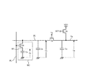
図23は、従来の典型的な電荷転送型のセンスアンプ回路の構成例を示している。図23においては、N型の選択トランジスタQ0及びキャパシタCsからなるメモリセルMCと、2つのN型のMOSトランジスタQg、Qpと、ラッチ型差動アンプ100が示されている。選択トランジスタQ0は、ソースがビット線BLに接続され、ゲートがワード線WLに接続される。キャパシタCsは、選択トランジスタQ0のドレインとグランド電位の間に接続される。MOSトランジスタQgは、ゲートに印加された制御電圧Vgに応じて、ビット線BLとセンスノードNsとの間の接続を制御する。MOSトランジスタQpは、ゲートに印加された制御信号SETに応じて、電源電圧VDDとセンスノードNsとの間の接続を制御する。ラッチ型差動アンプ100は、センスノードNsの信号電圧と、参照電位Vrとをそれぞれ入力し、差動増幅してラッチする。なお、参照電位Vrは、メモリセルMCからハイ情報とロー情報をそれぞれ読み出したときのセンスノードNsにおける各電位の概ね中間電位に設定される。
FIG. 23 shows a configuration example of a conventional typical charge transfer type sense amplifier circuit. FIG. 23 shows a memory cell MC composed of an N-type selection transistor Q0 and a capacitor Cs, two N-type MOS transistors Qg and Qp, and a latch-type
図23において、ビット線BLにはビット線容量Cbが形成され、センスノードNsには容量Caが形成される。発明者らの検討により、センスアンプ回路において想定される動作モードは、キャパシタの容量Cs、ビット線BLの電位とビット線容量Cb、センスノードNsの電位と容量Ca(図1及びその説明を参照)などのパラメータに依存して定まり、後述の(式1)〜(式3)に従って動作することが見出された。図23に示す従来の電荷転送型のセンスアンプ回路については、前述の動作モードのうち、電荷転送モードが支配的になることが確認されている。
しかしながら、図23の電荷転送型のセンスアンプ回路を用いる場合は、比較的回路規模が大きいラッチ型差動アンプ100を採用しているため、センスノードNsの容量Caの増大が避けられない。例えば、1本のビット線BLに512個のメモリセルMCを設ける構成において、ビット線容量Cb=50fF程度に対し、センスノードNsの容量Ca=10fF程度になることが想定される。そして、かかる条件に基づき発明者らが検討を行った結果、電源電圧VDDが比較的高い場合(例えば、3Vや2V)、センスアンプ回路の増幅動作に支障はないものの、特に電源電圧VDDの低電圧化を図って、例えばVDD=1Vで動作させる場合、増幅動作に支障を来たすことが判明した(図5及び図6とその説明参照)。このような条件下では、メモリセルMCのハイ情報とロー情報をそれぞれ読み出したときにセンスノードNsにおける電圧差が小さくなり、動作マージンが十分確保できなくなる。また、このような傾向は、メモリセルMCを小型化して容量が小さいキャパシタCsを用いる場合には、一層顕著になることがわかった。以上のように、従来の電荷転送型センスアンプ回路は、低容量のメモリセルMCを用いて低電圧動作を図る構成に対して適用することが困難であるという問題がある。
However, when the charge transfer type sense amplifier circuit of FIG. 23 is used, since the latch type
そこで、本発明はこれらの問題を解決するためになされたものであり、キャパシタの容量が小さいメモリセルを採用した半導体記憶装置において低電圧動作を図る場合、電荷転送モードと電荷分配モードの増幅動作を適切に制御することにより、読み出し動作時に十分な動作マージンを確保することが可能なセンスアンプ回路を提供することを目的とする。 Accordingly, the present invention has been made to solve these problems, and in a semiconductor memory device employing a memory cell having a small capacity of a capacitor, when a low voltage operation is intended, an amplification operation in a charge transfer mode and a charge distribution mode. An object of the present invention is to provide a sense amplifier circuit capable of ensuring a sufficient operation margin during a read operation by appropriately controlling the above.
上記課題を解決するために、本発明のセンスアンプ回路は、メモリセルから読み出されてビット線を伝送される信号を増幅するシングルエンド型のセンスアンプ回路であって、ゲートに印加される制御電圧に応じて、前記ビット線に対して所定電位を供給するとともに、前記ビット線とセンスノードとの間の接続を制御する第1のMOSトランジスタと、ゲートが前記センスノードに接続され、前記ビット線から前記第1のMOSトランジスタを介して伝送される信号を増幅する第2のMOSトランジスタとを備えて構成され、前記メモリセルの読み出し動作に先立って前記所定電位が前記ビット線に供給されるとともに、当該所定電位は、前記メモリセルの読み出し電圧の範囲内において電荷転送モードと電荷分配モードとが切り換わる変化点の近傍で、前記メモリセルのハイ情報とロー情報をそれぞれ読み出した際に前記センスノードにおける所要の電圧差を確保可能な値に設定されることを特徴とする。 In order to solve the above problems, a sense amplifier circuit of the present invention is a single-ended sense amplifier circuit that amplifies a signal read from a memory cell and transmitted through a bit line, and is applied to a gate. A first MOS transistor for supplying a predetermined potential to the bit line according to a voltage and controlling connection between the bit line and a sense node, and a gate connected to the sense node, And a second MOS transistor for amplifying a signal transmitted from the line through the first MOS transistor, and the predetermined potential is supplied to the bit line prior to the read operation of the memory cell. In addition, the predetermined potential changes so that the charge transfer mode and the charge distribution mode are switched within the range of the read voltage of the memory cell. In the vicinity of the point, characterized in that it is set high information and low information of the memory cell to possible values ensure the required voltage difference at the sense node when the read respectively.
本発明のセンスアンプ回路によれば、メモリセルの読み出し動作に際し、第1のMOSトランジスタが制御電圧に応じた所定電位をビット線に供給した状態で、第1のMOSトランジスタが電荷転送ゲートとして機能し、電荷転送モードあるいは電荷分配モードに基づき、センスノードに接続される第2のMOSトランジスタによって信号電圧が増幅される。このとき、メモリセルのハイ情報とロー情報を読み出す場合、両者の電圧差が十分確保されるように電位関係が設定されるとともに、シングルエンド型を採用したためにセンスノードの容量を小さくできるので、低容量のメモリセルを採用した場合であっても、特に低電圧動作時の動作マージンの向上に有効な構成を実現することができる。 According to the sense amplifier circuit of the present invention, in the memory cell read operation, the first MOS transistor functions as a charge transfer gate in a state where the first MOS transistor supplies a predetermined potential corresponding to the control voltage to the bit line. Then, based on the charge transfer mode or the charge distribution mode, the signal voltage is amplified by the second MOS transistor connected to the sense node. At this time, when reading the high information and low information of the memory cell, the potential relationship is set so as to ensure a sufficient voltage difference between the two, and since the single end type is adopted, the capacitance of the sense node can be reduced. Even when a low-capacity memory cell is employed, it is possible to realize a configuration that is effective for improving the operation margin particularly during low-voltage operation.
本発明のセンスアンプ回路は、特に階層化されたメモリセルアレイに適用する場合に有効である。すなわち、所定数のローカルビット線がローカルセンスアンプを介してグローバルビット線と選択的に接続される構成において、差動構成を採用することなくシングルエンド型のローカルセンスアンプを用いて回路規模の小型化を図りつつ、センスアンプ回路の動作マージンを十分に確保することができる。 The sense amplifier circuit of the present invention is particularly effective when applied to a hierarchical memory cell array. That is, in a configuration in which a predetermined number of local bit lines are selectively connected to a global bit line via a local sense amplifier, the circuit scale is small using a single-ended local sense amplifier without adopting a differential configuration. Thus, a sufficient operation margin of the sense amplifier circuit can be secured.
また、本発明のセンスアンプ回路は、特に、第1のMOSトランジスタ又は第2のMOSトランジスタの閾値電圧の変動が補償された補償電圧を発生する補償電圧発生回路と組み合わせて用いることが有効である。このような補償電圧をセンスアンプ回路に供給することにより、上述の動作マージンをより一層向上させることが可能となる。 In addition, the sense amplifier circuit of the present invention is particularly effective when used in combination with a compensation voltage generation circuit that generates a compensation voltage in which variation in threshold voltage of the first MOS transistor or the second MOS transistor is compensated. . By supplying such a compensation voltage to the sense amplifier circuit, the above-described operation margin can be further improved.
以上述べたように本発明によれば、シングルエンド型のセンスアンプを採用し、電荷転送モードと電荷分配モードに基いて増幅動作を制御する場合、センスノードの容量を小さく設定できるので、1V程度の低電圧動作における動作マージンを十分に確保することができる。特に、5fF以下のように小さい容量のメモリセルを用いる場合に有利な構成を実現できる。 As described above, according to the present invention, when a single-ended sense amplifier is employed and the amplification operation is controlled based on the charge transfer mode and the charge distribution mode, the capacitance of the sense node can be set small, so that it is about 1V. A sufficient operating margin can be secured in the low voltage operation. In particular, an advantageous configuration can be realized when a memory cell having a small capacity of 5 fF or less is used.
また、ビット線構成とセンスアンプ回路が階層化された半導体記憶装置において、特にローカルビット線の容量を小さく設定できるので、大容量の半導体記憶装置において良好な動作マージンを実現可能となる。 Further, in the semiconductor memory device in which the bit line configuration and the sense amplifier circuit are hierarchized, since the capacity of the local bit line can be set particularly small, a good operation margin can be realized in a large capacity semiconductor memory device.
さらに、補償電圧発生回路を用いることで、MOSトランジスタの閾値電圧の製造プロセスや温度による変動を適切に補償することができ、センス時の動作マージンを一層向上させ、センスアンプ回路の動作の信頼性を高めることができる。あるいは、チップ内のばらつき許容範囲を拡大することができるので、小さい容量のメモリセルを用いる大容量のDRAMに多数のセンスアンプ回路を組み込む場合、製造歩留まりの向上と製造コストの低減が可能となる。 Furthermore, by using the compensation voltage generation circuit, it is possible to appropriately compensate for variations in the threshold voltage of the MOS transistor due to the manufacturing process and temperature, further improve the operating margin during sensing, and improve the operational reliability of the sense amplifier circuit. Can be increased. Alternatively, since the tolerance range within the chip can be expanded, when a large number of sense amplifier circuits are incorporated in a large capacity DRAM using a small capacity memory cell, the manufacturing yield can be improved and the manufacturing cost can be reduced. .
本発明の実施形態について図面を参照しながら説明する。以下では、センスアンプ回路を備えた半導体記憶装置に対して本発明を適用した3つの実施形態について説明する。 Embodiments of the present invention will be described with reference to the drawings. Hereinafter, three embodiments in which the present invention is applied to a semiconductor memory device including a sense amplifier circuit will be described.
[基本原理]
まず、本実施形態のセンスアンプ回路に関し、基本的な動作原理について図1を参照して説明する。以下では、センスアンプ回路の動作モードとして、主に電荷転送モード(チャージトランスファモード)と電荷分配モード(チャージシェアモード)を想定する。図1は、電荷転送モード及び電荷分配モードで動作するセンスアンプ回路の入力側の構成を模式的に示す図である。図1においては、N型の選択トランジスタQ0及びキャパシタCsからなるメモリセルMCと、2つのN型のMOSトランジスタQg、Qpからなるセンスアンプ回路が示されている。
[Basic principle]
First, regarding the sense amplifier circuit of this embodiment, the basic operation principle will be described with reference to FIG. In the following, it is assumed that the operation mode of the sense amplifier circuit is mainly a charge transfer mode (charge transfer mode) and a charge distribution mode (charge share mode). FIG. 1 is a diagram schematically showing a configuration on the input side of a sense amplifier circuit that operates in a charge transfer mode and a charge distribution mode. FIG. 1 shows a memory cell MC composed of an N-type selection transistor Q0 and a capacitor Cs, and a sense amplifier circuit composed of two N-type MOS transistors Qg and Qp.
選択トランジスタQ0は、ソースがビット線BLに接続され、ゲートがワード線WLに接続される。また、選択トランジスタQ0のドレインとグランド電位の間にキャパシタCsが接続される。電荷転送ゲートとして機能するMOSトランジスタQgは、ビット線BLとセンスノードNsとの間に接続されている。ビット線電位供給用のMOSトランジスタQpは、電源電圧VDDとセンスノードNsとの間に接続されている。MOSトランジスタQgのゲートには制御電圧Vgが印加され、MOSトランジスタQpのゲートには制御信号SETが印加されている。図1には、ビット線BLに形成されるビット線容量Cbと、センスノードNsに形成される容量Caと、ビット線BLの電位Vbと、センスノードNsの電位Vaをそれぞれ示している。このうち、ビット線容量Cb及びセンスノードNsの容量Caは、配線の寄生容量、トランジスタ等の入力容量、メモリセルMCの接続数などに依存して定まる。 The selection transistor Q0 has a source connected to the bit line BL and a gate connected to the word line WL. A capacitor Cs is connected between the drain of the selection transistor Q0 and the ground potential. The MOS transistor Qg functioning as a charge transfer gate is connected between the bit line BL and the sense node Ns. The bit line potential supply MOS transistor Qp is connected between the power supply voltage VDD and the sense node Ns. A control voltage Vg is applied to the gate of the MOS transistor Qg, and a control signal SET is applied to the gate of the MOS transistor Qp. FIG. 1 shows a bit line capacitance Cb formed on the bit line BL, a capacitance Ca formed on the sense node Ns, a potential Vb on the bit line BL, and a potential Va on the sense node Ns. Among these, the bit line capacitance Cb and the capacitance Ca of the sense node Ns are determined depending on the parasitic capacitance of the wiring, the input capacitance of the transistor, the number of connected memory cells MC, and the like.
メモリセルMCの読み出し動作に先立って、ビット線電位供給用のMOSトランジスタQpの動作により、センスノードNsが電源電圧VDDに設定される。このとき、ビット線BLは、MOSトランジスタQgを介して、制御電圧VgとMOSトランジスタQgの閾値電圧Vt1に基づき、Vb=Vg−Vt1となる電位Vb(本発明の所定電位)が供給される。 Prior to the read operation of the memory cell MC, the sense node Ns is set to the power supply voltage VDD by the operation of the MOS transistor Qp for supplying the bit line potential. At this time, the bit line BL is supplied with the potential Vb (the predetermined potential of the present invention) satisfying Vb = Vg−Vt1 based on the control voltage Vg and the threshold voltage Vt1 of the MOS transistor Qg via the MOS transistor Qg.
その後、MOSトランジスタQpがオフし、続いてワード線WLが駆動されて選択トランジスタQ0がオンする。これにより、センスアンプ回路によるセンス動作が開始される。このときのメモリセルMCの電荷蓄積ノードN0の電圧をVsとすると、Vs、Vb、VDDの各値の関係に応じて、次の3つの動作に分けることができる。
(1)MOSトランジスタQgがオフを保持
(2)MOSトランジスタQgを通して上述の電荷転送モードで電荷が移動
(3)MOSトランジスタQgを通して上述の電荷分配モードで電荷が移動
Thereafter, the MOS transistor Qp is turned off, and then the word line WL is driven to turn on the selection transistor Q0. Thereby, the sensing operation by the sense amplifier circuit is started. If the voltage of the charge storage node N0 of the memory cell MC at this time is Vs, it can be divided into the following three operations according to the relationship between the values of Vs, Vb, and VDD.
(1) MOS transistor Qg is kept off (2) Charge is transferred in the above-described charge transfer mode through MOS transistor Qg (3) Charge is transferred in the above-described charge distribution mode through MOS transistor Qg
ここで、上記の動作(2)と動作(3)の境界(変化点)となる電位VbをVcと定義する。この電圧Vcを用いると、上記動作を完了した後のセンスノードNsの電位Vaは、動作(1)、(2)、(3)に対応して、それぞれ以下の(式1)、(式2)、(式3)のように表現される。
(式1)Vb≦Vs : Va=VDD
(式2)Vs<Vb≦Vc : Va=VDD+(Cs/Ca)Vs
−(Cs/Ca)Vb
(式3)Vc<Vb : Va=(CsVs+CaVDD)/(Cs+Cb+Ca)
+(Cb/(Cs+Cb+Ca))Vb
Here, the potential Vb that becomes the boundary (change point) between the above-described operations (2) and (3) is defined as Vc. When this voltage Vc is used, the potential Va of the sense node Ns after the above operation is completed corresponds to the operations (1), (2), and (3), respectively (Equation 1) and (Equation 2) below. ) And (Expression 3).
(Formula 1) Vb ≦ Vs: Va = VDD
(Expression 2) Vs <Vb ≦ Vc: Va = VDD + (Cs / Ca) Vs
-(Cs / Ca) Vb
(Expression 3) Vc <Vb: Va = (CsVs + CaVDD) / (Cs + Cb + Ca)
+ (Cb / (Cs + Cb + Ca)) Vb
ただし、電圧Vcは次式で算出される。
Vc=((Cs+Cb)CaVDD)+(Cs+Cb)CsVs)
/(Cs(Cs+Cb+Ca)+CbCa)
However, the voltage Vc is calculated by the following equation.
Vc = ((Cs + Cb) CaVDD) + (Cs + Cb) CsVs)
/ (Cs (Cs + Cb + Ca) + CbCa)
例えば、図23に示す従来のセンスアンプは、主に上記式(2)の電荷転送モードにより動作させるものであるが(電荷転送型センスアンプ)、本実施形態のセンスアンプ回路は、電荷転送モードと電荷分配モードとを制御しつつ動作させることが特徴である。 For example, the conventional sense amplifier shown in FIG. 23 is mainly operated in the charge transfer mode of the above formula (2) (charge transfer type sense amplifier), but the sense amplifier circuit of the present embodiment is in charge transfer mode. And the charge distribution mode are controlled.
[第1実施形態]
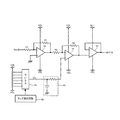
以下、本発明の第1実施形態について説明する。第1実施形態では、電荷転送・電荷分配制御型のシングルエンドセンスアンプ回路を採用した点が特徴である。図2は、第1実施形態のDRAMのうちセンス系の回路構成の一例を示す図であり、メモリセルMCと、上述のセンスアンプ回路の基本動作を担うプリアンプ10(本発明の第1のセンスアンプ)と、プリアンプ10の後段のセンスラッチ回路11(本発明の第2のセンスアンプ)が示されている。
[First Embodiment]
The first embodiment of the present invention will be described below. The first embodiment is characterized in that a charge transfer / charge distribution control type single-end sense amplifier circuit is employed. FIG. 2 is a diagram showing an example of a sense circuit configuration in the DRAM of the first embodiment. The memory cell MC and the
メモリセルMCは、NMOS型の選択トランジスタQ0と、情報を電荷として保持するキャパシタCsとから構成される1T1C型のDRAMメモリセルである。選択トランジスタQ0は、ソースがビット線BLに接続され、ゲートがワード線WLに接続されている。キャパシタCsは、選択トランジスタQ0のドレインとセルプレート電位VPLTとの間に接続されている。図2では、1つのメモリセルMCを示しているが、実際には複数のワード線WLと複数のビット線BLの各交点に配置された多数のメモリセルMCが設けられている。第1実施形態では、例えば、1本のビット線BLに512個のメモリセルMCが接続されることを想定する。この場合、1本のビット線BLに形成されるビット線容量Cbは、全体として例えば50fFとなる。 The memory cell MC is a 1T1C type DRAM memory cell including an NMOS type select transistor Q0 and a capacitor Cs that holds information as electric charges. The selection transistor Q0 has a source connected to the bit line BL and a gate connected to the word line WL. The capacitor Cs is connected between the drain of the selection transistor Q0 and the cell plate potential VPLT. Although one memory cell MC is shown in FIG. 2, in reality, a large number of memory cells MC arranged at each intersection of a plurality of word lines WL and a plurality of bit lines BL are provided. In the first embodiment, for example, it is assumed that 512 memory cells MC are connected to one bit line BL. In this case, the bit line capacitance Cb formed in one bit line BL is, for example, 50 fF as a whole.
プリアンプ10は、5つのN型のMOSトランジスタQ1、Q2、Q3、Q4、Q5から構成されている。電荷転送ゲートとして機能するMOSトランジスタQ1(本発明の第1のMOSトランジスタ)は、ビット線BLとプリアンプ10側のセンスノードNsの間に接続され、ゲートに制御電圧Vgが印加されている。増幅素子として機能するMOSトランジスタQ2(本発明の第2のMOSトランジスタ)は、ゲートがセンスノードNsに接続され、ビット線BLからMOSトランジスタQ1を介して伝送された信号をセンス・増幅してドレイン電流に変換する。このドレイン電流は、プリアンプ10の側の入出力ノードN1からMOSトランジスタQ4、Q2を通ってグランドに流れる。
The
ビット線BLのプリチャージ用トランジスタとして機能するMOSトランジスタQ3は、ゲートにプリチャージ信号PCが印加され、プリチャージ信号PCがハイのときにセンスノードNsをグランド電位にプリチャージする。センスノードNsがプリチャージされると、MOSトランジスタQ1を介してビット線BLがグランド電位にプリチャージされる。読み出し制御用のMOSトランジスタQ4は、ゲートに印加される制御信号RTに応じて、入出力ノードN1とMOSトランジスタQ2との間の接続を制御する。書き込み制御用のMOSトランジスタQ5は、ゲートに印加される制御信号WTに応じて、入出力ノードN1とセンスノードNsとの間の接続を制御する。 In the MOS transistor Q3 functioning as a precharge transistor for the bit line BL, the precharge signal PC is applied to the gate, and when the precharge signal PC is high, the sense node Ns is precharged to the ground potential. When the sense node Ns is precharged, the bit line BL is precharged to the ground potential via the MOS transistor Q1. The read control MOS transistor Q4 controls the connection between the input / output node N1 and the MOS transistor Q2 in accordance with a control signal RT applied to the gate. Write control MOS transistor Q5 controls connection between input / output node N1 and sense node Ns in accordance with control signal WT applied to the gate.
図2においては、プリアンプ10がMOSトランジスタ5個からなるシンプルな構成であるため、プリアンプ10内のセンスノードNsに形成される容量Caは、例えば、1〜2fF程度の値になり、上述のビット線容量Cbに比べて格段に小さい値になる。
In FIG. 2, since the
図3は、プリアンプ10の後段のセンスラッチ回路11の回路構成の一例を示している。図3に示すように、センスラッチ回路11には、入出力ノードN1、読み出し信号線/RDL、書き込み信号線/WDLが接続され、3個のP型のMOSトランジスタQ10、Q13、Q15と8個のN型のMOSトランジスタQ11、Q12、Q14、Q16〜Q20を含んで構成される。電源電圧VDDと入出力ノードN1との間には、プリチャージ用のMOSトランジスタQ10が接続されている。MOSトランジスタQ10は、ゲートに印加される反転プリチャージ信号/PCがローのときに入出力ノードN1を電源電圧VDDにプリチャージする。MOSトランジスタQ11は、ゲートに印加されるラッチ制御信号LTCに応じて、入出力ノードN1とノードN2との間の接続を制御する。また、MOSトランジスタQ12は、ゲートに印加される制御信号RESに応じて、入出力ノードN1とノードN3との間の接続を制御する。
FIG. 3 shows an example of the circuit configuration of the
信号電圧判定ラッチ11aは、MOSトランジスタQ13、Q14、Q15、Q16から構成され、プリアンプ10から入出力ノードN1に伝送された信号電位を2値で判定してラッチする。信号電圧判定ラッチ11aにおいて、それぞれゲートがノードN2に接続される一対のMOSトランジスタQ13、Q14により、比較的駆動力の大きなセンス用インバータが構成される。同様に、それぞれゲートがノードN3に接続される一対のMOSトランジスタQ15、Q16により、比較的駆動力の小さなラッチ用インバータが構成される。
The signal
読み出し信号線/RDLとグランドの間には、読み出し回路としての2つのMOSトランジスタQ17、Q18が直列接続され、信号電圧判定ラッチ11aの出力信号SD(ノードN3)がMOSトランジスタQ17のゲートに入力される。書き込み信号線/WDLとノードN2の間には、書き込み回路としての2つのMOSトランジスタQ19、Q20が直列接続され、MOSトランジスタQ19のゲートに書き込みイネーブル信号WEが入力される。MOSトランジスタQ18、Q20の各ゲートには、センスアンプ選択信号YSが共通に入力される。
Two MOS transistors Q17 and Q18 as a read circuit are connected in series between the read signal line / RDL and the ground, and the output signal SD (node N3) of the signal
読み出し動作時は、ラッチ制御信号LTCがハイ、かつセンスアンプ選択信号YSがハイになり、センス用インバータの出力信号SDが読み出し信号線/RDLに出力される。このとき、ノードN3に現れる出力信号SDは、入出力ノードN1の論理値を反転した電圧となっている。また、読み出し動作後のメモリセルMCのデータの破壊を回避するための再書き込み動作時は、ラッチ制御信号LTCがロー、制御信号RESがハイとなり、出力信号SDはMOSトランジスタQ12を介して入出力ノードN1に出力される。 During the read operation, the latch control signal LTC is high and the sense amplifier selection signal YS is high, and the output signal SD of the sense inverter is output to the read signal line / RDL. At this time, the output signal SD appearing at the node N3 is a voltage obtained by inverting the logic value of the input / output node N1. At the time of a rewrite operation for avoiding the destruction of data in the memory cell MC after the read operation, the latch control signal LTC is low, the control signal RES is high, and the output signal SD is input / output via the MOS transistor Q12. Output to the node N1.
一方、書き込み動作時は、センスアンプ選択信号YSがハイ、書き込みイネーブル信号WEがハイになり、書き込み信号線/WDLから書き込みデータが入力される。この書き込みデータは、上述のセンス用インバータにより反転され、MOSトランジスタQ12を介して入出力ノードN1に出力される。 On the other hand, during the write operation, the sense amplifier selection signal YS is high, the write enable signal WE is high, and write data is input from the write signal line / WDL. This write data is inverted by the above-described sensing inverter and output to the input / output node N1 via the MOS transistor Q12.
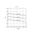
次に、第1実施形態のセンスアンプ回路の増幅動作について、図4を用いて説明する。図4は、第1実施形態のセンスアンプ回路の増幅動作を説明するために、2通りの容量の条件に対応する2つのグラフを示している。各グラフにおいて電源電圧VDD=1Vを想定し、特性W1(H)はメモリセルMCからハイ情報を読み出すときの特性であり(Vs=1V)、特性W1(L)は、メモリセルMCからロー情報を読み出すときの特性である(Vs=0V)。なお、電圧Vsは、キャパシタCsの電荷蓄積ノードN0の電圧である。また、ビット線容量Cbと、メモリセルMCのキャパシタCsの容量(以下、単に容量Csと呼ぶ)と、センスノードNsの容量Caに関し、図4(a)では、Cb=50fF、Cs=5fF、Ca=2fFに設定され、図4(b)では、Cb=50fF、Cs=2fF、Ca=1fFに設定されるとする。 Next, the amplification operation of the sense amplifier circuit of the first embodiment will be described with reference to FIG. FIG. 4 shows two graphs corresponding to two capacitance conditions in order to explain the amplification operation of the sense amplifier circuit of the first embodiment. In each graph, assuming that the power supply voltage VDD = 1V, the characteristic W1 (H) is a characteristic when high information is read from the memory cell MC (Vs = 1V), and the characteristic W1 (L) is low information from the memory cell MC. (Vs = 0V). The voltage Vs is the voltage at the charge storage node N0 of the capacitor Cs. Further, regarding the bit line capacitance Cb, the capacitance of the capacitor Cs of the memory cell MC (hereinafter simply referred to as the capacitance Cs), and the capacitance Ca of the sense node Ns, in FIG. 4A, Cb = 50 fF, Cs = 5 fF, Assume that Ca = 2fF, and in FIG. 4B, Cb = 50fF, Cs = 2fF, and Ca = 1fF.
図4において、ハイ情報の読み出し時の特性W1(H)は、電源電圧VDDが1Vであるため、上述の(式1)に従って、電位Vbの変化に対して電位Vaが1Vに保たれる。一方、ロー情報の読み出し時の特性W1(L)は、変化点P1までの領域(P1の左側)では上述の(式2)に従って電荷転送モードで動作し、変化点P1を過ぎた領域(P1の右側)では上述の(式3)に従って電荷分配モードで動作する。各グラフにおいて、特性W1(H)と特性W1(L)との電圧差により信号電圧の読み出し可能な範囲が定まる。 In FIG. 4, the characteristic W1 (H) at the time of reading high information is that the power supply voltage VDD is 1V, so that the potential Va is maintained at 1V with respect to the change in the potential Vb according to the above (Equation 1). On the other hand, the characteristic W1 (L) at the time of reading row information operates in the charge transfer mode according to (Equation 2) described above in the region up to the change point P1 (left side of P1), and the region (P1) past the change point P1. In the right side), the operation is performed in the charge distribution mode according to (Equation 3) described above. In each graph, a signal voltage readable range is determined by a voltage difference between the characteristic W1 (H) and the characteristic W1 (L).
図4には、プリアンプ10における閾値電圧のばらつき許容範囲Rvt1の設定例を重ねて示している。ばらつき許容範囲Rvt1の縦軸方向の幅は、MOSトランジスタQ2の閾値電圧Vt2のばらつき許容範囲を表し、ばらつき許容範囲Rvt1の横軸方向の幅は、MOSトランジスタQ1の閾値電圧Vt1のばらつき許容範囲を表している。なお、電位Vbは、MOSトランジスタQ1の一定の制御電圧Vgから、MOSトランジスタQ1の閾値電圧Vt1だけ低い電圧に設定される。図4の例では、MOSトランジスタQ2の閾値電圧Vt2のばらつき許容範囲が0.5〜0.8V、MOSトランジスタQ1の閾値電圧Vt1のばらつき許容範囲が0.2〜0.5Vにある。このように、ばらつき許容範囲Rvt1が全体的に特性W1(H)、W1(L)に囲まれた範囲内に存在することが、プリアンプ10による安定な増幅動作の条件となる。この場合、特性W1(H)、W1(L)に囲まれた範囲内でばらつき許容範囲Rvt1が大きいほど、動作マージンが大きくなり増幅動作の信頼性が向上する。
In FIG. 4, setting examples of the threshold voltage variation allowable range Rvt1 in the
ここで、図4に対する比較例として、従来のセンスアンプ回路(図23)の増幅動作に対応する2通りのグラフを図5及び図6に示す。図5及び図6の各々においては、電源電圧VDDの3Vまでの動作を想定し、VDD=3V、2V、1Vの場合の3通りについて、それぞれハイ情報とロー情報を読み出す場合の特性を示している。また、図5では、図4(a)に対応してCs=5fFに設定され、図6では、図4(b)に対応してCs=2fFに設定されるとする。図5及び図6においては、ともにCb=50fF、Ca=10fFに設定されるとする。図5においては、特性W、変化点P、横軸方向及び縦軸方向の各許容範囲X、Yのそれぞれに対し、カッコ書きにてVDDの値(3、2、1)とハイ情報(H)/ロー情報(L)を付加して表している。図6においても、特性W’、変化点P’、横軸方向及び縦軸方向の各許容範囲X’、Y’のそれぞれに対し、同様に表している。ここでX及びX’は電位Vbの設定値の許容範囲を、Y及びY’は許容範囲X及びX’におけるハイ情報とロー情報の読み出し信号電圧の差を示している。 Here, as a comparative example for FIG. 4, two graphs corresponding to the amplification operation of the conventional sense amplifier circuit (FIG. 23) are shown in FIGS. In each of FIGS. 5 and 6, assuming the operation up to 3V of the power supply voltage VDD, the characteristics in the case of reading out the high information and the low information are shown for the three cases of VDD = 3V, 2V, and 1V, respectively. Yes. 5, Cs = 5 fF is set corresponding to FIG. 4A, and Cs = 2 fF is set corresponding to FIG. 4B in FIG. 6. 5 and 6, it is assumed that both Cb = 50 fF and Ca = 10 fF are set. In FIG. 5, VDD values (3, 2, 1) and high information (H) are written in parentheses for each of the allowable range X, Y in the characteristic W, change point P, horizontal axis direction and vertical axis direction. ) / Raw information (L) is added. Also in FIG. 6, the characteristic W ′, the change point P ′, and the permissible ranges X ′ and Y ′ in the horizontal axis direction and the vertical axis direction are similarly represented. Here, X and X ′ indicate the allowable range of the set value of the potential Vb, and Y and Y ′ indicate the difference between the read signal voltages of the high information and the low information in the allowable ranges X and X ′.
従来のセンスアンプ回路では、電源電圧VDD=3V、2Vの場合、変化点P、P’の位置が右側にシフトしており、電荷転送モードが支配的であることがわかる。この場合、Cs=5fFの図5に比べ、メモリセルMCを低容量化したCs=2fFの図6は、読み出し電圧の信号差が小さくなっている。また、図5及び図6から明らかなように、VDD=1Vの条件では、上述の許容範囲X、Yを確保することが困難であり、かかる低電圧動作で従来のセンスアンプ回路を用いることは困難である。このように、特にVDD=1Vの低電圧動作の条件下で、上述の図4の場合において、図5及び図6の動作と比べたときに動作マージンが大幅に向上する点で顕著な相違がある。これは、主にシングルエンド型のプリアンプ10を採用したことにより、センスノードNsの容量Caを減少することによる効果である。なお、図4(a)においては、図5におけるVDD=1Vのときの特性W(1L)を破線で示すとともに、図4(b)においては、図6におけるVDD=1Vのときの特性W’(1L)を破線で示し、それぞれを比較している。
In the conventional sense amplifier circuit, when the power supply voltage VDD = 3V and 2V, the positions of the change points P and P ′ are shifted to the right side, and it can be seen that the charge transfer mode is dominant. In this case, compared with FIG. 5 with Cs = 5 fF, the signal difference of the read voltage is smaller in FIG. 6 with Cs = 2 fF in which the capacity of the memory cell MC is reduced. Further, as apparent from FIGS. 5 and 6, it is difficult to ensure the above-described allowable ranges X and Y under the condition of VDD = 1V, and it is difficult to use a conventional sense amplifier circuit in such a low voltage operation. Have difficulty. As described above, particularly in the case of the above-described FIG. 4 under the condition of the low voltage operation of VDD = 1V, there is a remarkable difference in that the operation margin is greatly improved when compared with the operations of FIG. 5 and FIG. is there. This is an effect of reducing the capacitance Ca of the sense node Ns mainly by adopting the single-ended
[第2実施形態]
次に、本発明の第2実施形態について説明する。第2実施形態は、階層化されたメモリセルアレイが構成され、ビット線とセンスアンプ回路がともに階層化されたDRAMに対し、電荷転送・電荷分配制御型のシングルエンドセンスアンプを適用したものである。図7は、第2実施形態のDRAMのうちセンス系の回路構成の一例を示す図であり、メモリセルMCと、階層化されたビット線としてのローカルビット線LBL及びグローバルビット線GBLと、階層化されたセンスアンプ回路としてのローカルセンスアンプ20及びグローバルセンスアンプ21とが示されている。メモリセルMCが接続されたローカルビット線LBLは、ローカルセンスアンプ20を介して選択的にグローバルビット線GBLに接続され、さらに対応するグローバルセンスアンプ21に伝送される。また、図7では一部のみが図示されるが、第2実施形態においては、各々のローカルセンスアンプ20を両側のローカルビット線LBLが共有するとともに、各々のグローバルセンスアンプ21を両側のグローバルビット線GBLが共有する構成が採用される。これにより、ローカルセンスアンプ20とグローバルセンスアンプ21の個数を減らしてチップ面積の削減が可能となる。
[Second Embodiment]
Next, a second embodiment of the present invention will be described. In the second embodiment, a hierarchical memory cell array is configured, and a charge transfer / charge distribution control type single-ended sense amplifier is applied to a DRAM in which bit lines and sense amplifier circuits are both hierarchized. . FIG. 7 is a diagram illustrating an example of a sense circuit configuration in the DRAM of the second embodiment. The memory cell MC, the local bit line LBL and the global bit line GBL as hierarchical bit lines, A
メモリセルMCの構造は、第1実施形態の図2と同様である。第2実施形態においては、1本のローカルビット線LBLに、例えば、32個のメモリセルMCが接続されるものとする。この場合、ローカルビット線LBLに形成されるビット線容量Cbは、例えば、Cb=3fFとなる。また、1つのローカルセンスアンプ20は2本のローカルビット線LBLに共有されるので、64個のメモリセルMCが接続されることになる。ローカルセンスアンプ20の回路構成のうち、MOSトランジスタQ1〜Q5を含む部分は第1実施形態のプリアンプ10と共通する。一方、ローカルセンスアンプ20においては、一方のローカルビット線LBLの電荷転送ゲートとして機能するMOSトランジスタQ1に加えて、他方のローカルビット線LBL(ノードN10)の電荷転送ゲートとして機能するMOSトランジスタQ6が付加されている。図7の左側のMOSトランジスタQ1のゲートには制御信号CTLが印加され、図7の右側のMOSトランジスタQ6のゲートには制御信号CTRが印加されている。
The structure of the memory cell MC is the same as that of FIG. 2 of the first embodiment. In the second embodiment, for example, 32 memory cells MC are connected to one local bit line LBL. In this case, the bit line capacitance Cb formed in the local bit line LBL is, for example, Cb = 3 fF. Since one
また、1本のグローバルビット線GBLには、例えば、8個のローカルセンスアンプ20が接続されものとする。この場合、1本のグローバルビット線GBLには、合計で512個のメモリセルMCを選択的に接続可能となる。各々のグローバルビット線GBLには、寄生容量Cgbが形成されている。グローバルセンスアンプ21の両側には、一方のグローバルビット線GBLとの間の接続を制御するMOSトランジスタQ7と、他方のグローバルビット線GBLとの間の接続を制御するMOSトランジスタQ8が設けられている。そして、MOSトランジスタQ7のゲートに印加される制御信号SHLと、MOSトランジスタQ8のゲートに印加される制御信号SHRにより、両側のグローバルビット線GBLとグローバルセンスアンプ21を選択的に接続することができる。
Also, for example, eight
図8は、グローバルセンスアンプ21の回路構成の一例を示している。図8に示すように、グローバルセンスアンプ21は第1実施形態のセンスラッチ回路11(図3)と概ね同様の回路構成を有するので、説明を省略する。ただし、図3の入出力ノードN1に対応する図8のノードN12は、グローバルセンスアンプ21を挟んだ両側の上記2つのMOSトランジスタQ7、Q8に接続されている点で相違がある。
FIG. 8 shows an example of the circuit configuration of the
図9は、第2実施形態のセンスアンプ回路の増幅動作を説明するための2つのグラフを示している。図9に示す2つのグラフは、第1実施形態の図4と同様に電位Va、Vbの関係について2通りの容量の条件に対応する。特性W2(H)はメモリセルMCからハイ情報を読み出すときの特性であり(Vs=1V)、特性W2(L)は、メモリセルMCからロー情報を読み出すときの特性である(Vs=0V)。また、ビット線容量Cbと、メモリセルMCの容量Csと、センスノードNsの容量Caに関し、図9(a)では、Cb=3fF、Cs=5fF、Ca=2fFに設定され、図9(b)は、Cb=3fF、Cs=2fF、Ca=1fFに設定されるとする。その他の条件については、図4の場合と同様である。 FIG. 9 shows two graphs for explaining the amplification operation of the sense amplifier circuit of the second embodiment. The two graphs shown in FIG. 9 correspond to two capacitance conditions regarding the relationship between the potentials Va and Vb, as in FIG. 4 of the first embodiment. The characteristic W2 (H) is a characteristic when reading high information from the memory cell MC (Vs = 1V), and the characteristic W2 (L) is a characteristic when reading low information from the memory cell MC (Vs = 0V). . Further, regarding the bit line capacitance Cb, the capacitance Cs of the memory cell MC, and the capacitance Ca of the sense node Ns, in FIG. 9A, Cb = 3fF, Cs = 5fF, and Ca = 2fF are set. ) Is set to Cb = 3 fF, Cs = 2 fF, and Ca = 1 fF. Other conditions are the same as in the case of FIG.
図9には、図4と同様、閾値電圧のばらつき許容範囲Rvt2の設定例を重ねて示している。図9のグラフを、図4のグラフと比較すると、特性W2(H)、W2(L)で囲まれた範囲内で、ばらつき許容範囲Rvt2を大きく設定できることがわかる。すなわち、ローカルセンスアンプ20の動作マージンが増加することを意味する。これはビット線構成が階層化された結果、ローカルビット線LBLのビット線容量Cbが減少したことの効果である。また、上述したように、しきい値電圧Vt1を有するMOSトランジスタQ1を介して、ローカルビット線LBLが電位Vb=Vg−Vt1に駆動されるが、その動作に要する時間がビット線容量Cbの減少に伴って短縮されるため、高速な読み出し動作が可能となる効果もある。
In FIG. 9, similarly to FIG. 4, setting examples of the threshold voltage variation allowable range Rvt <b> 2 are shown in an overlapping manner. Comparing the graph of FIG. 9 with the graph of FIG. 4, it can be seen that the variation allowable range Rvt2 can be set large within the range surrounded by the characteristics W2 (H) and W2 (L). That is, the operation margin of the
次に、第2実施形態のDRAMにおける読み出し動作について図10及び図11を参照して説明する。図10は、メモリセルMCからハイ情報を読み出す場合の動作波形を示す図であり、図11は、メモリセルMCからロー情報を読み出す場合の動作波形を示す図である。図10及び図11の上部に示すように、全体動作を6つの期間(T1〜T6)に細分化して示している。 Next, a read operation in the DRAM of the second embodiment will be described with reference to FIGS. FIG. 10 is a diagram illustrating an operation waveform when high information is read from the memory cell MC, and FIG. 11 is a diagram illustrating an operation waveform when low information is read from the memory cell MC. As shown in the upper part of FIG. 10 and FIG. 11, the entire operation is divided into six periods (T1 to T6).
図10に示すように、ハイ情報の読み出し動作では、プリチャージ解除期間T1の前の時点でローカルビット線LBL及びセンスノードNsはグランド電位VSS(0V)にプリチャージされており、グローバルビット線GBLは電源電圧VDDにプリチャージされている。このとき、プリチャージ信号PC、制御信号SHR、CTL、CTR、ラッチ制御信号LTCはそれぞれハイ、反転プリチャージ信号/PC、制御信号WT、RT、RESはそれぞれローになっている。 As shown in FIG. 10, in the high information read operation, the local bit line LBL and the sense node Ns are precharged to the ground potential VSS (0 V) before the precharge release period T1, and the global bit line GBL Is precharged to the power supply voltage VDD. At this time, the precharge signal PC, the control signals SHR, CTL, and CTR, and the latch control signal LTC are respectively high, and the inverted precharge signal / PC and the control signals WT, RT, and RES are each low.
プリチャージ解除期間T1において、プリチャージ信号PCがローに制御されてMOSトランジスタQ3がオフし、ローカルビット線LBL及びセンスノードNsはグランド電位VSSにプリチャージされた状態でフローティングとなる。また制御信号SHR、CTRがともにローに制御され、非選択側のグローバルビット線GBLがグローバルセンスアンプ21から切り離されるとともに、非選択側のローカルビット線LBLがローカルセンスアンプ20から切り離される。ここで、制御信号CTLの電圧値は、上記の制御電圧Vgに設定される。なお、非選択側のローカルセンスアンプ20については、プリチャージ信号PC、制御信号CTL、CTRがハイ、制御信号RT、WTがローに制御された状態に保たれる。
In the precharge release period T1, the precharge signal PC is controlled to be low, the MOS transistor Q3 is turned off, and the local bit line LBL and the sense node Ns are floated in a state of being precharged to the ground potential VSS. The control signals SHR and CTR are both controlled to be low, the unselected global bit line GBL is disconnected from the
ローカルビット線電位設定期間T2において、制御信号WTが正電圧VPPに制御され、その状態を一定期間保持する。正電圧VPPとなった制御信号WTによってMOSトランジスタQ5がオンし、ローカルセンスアンプ20内のセンスノードNsがグローバルビット線GBLを通して電源電圧VDDに駆動される。その結果、ローカルビット線LBLは、MOSトランジスタQ1を通して電圧Vg−Vt1に駆動される。その後、反転プリチャージ信号/PCがハイに制御され、グローバルビット線GBLが電源電圧VDDにプリチャージされた状態で保持される。
In the local bit line potential setting period T2, the control signal WT is controlled to the positive voltage VPP, and this state is maintained for a certain period. The MOS transistor Q5 is turned on by the control signal WT at the positive voltage VPP, and the sense node Ns in the
セル選択期間T3において、ワード線WLが負電圧VKKから正電圧VPPに駆動され、これによりハイ情報を保持するメモリセルMCの信号電圧がローカルビット線LBLに読み出される。このとき、ローカルビット線LBLの電位Vbは、電圧Vg−Vt1より高くなるので、MOSトランジスタQ1がオフの状態を保つ。よって、センスノードNsは電源電圧VDDの状態を保ち続ける。 In the cell selection period T3, the word line WL is driven from the negative voltage VKK to the positive voltage VPP, whereby the signal voltage of the memory cell MC holding high information is read out to the local bit line LBL. At this time, the potential Vb of the local bit line LBL becomes higher than the voltage Vg−Vt1, so that the MOS transistor Q1 is kept off. Therefore, the sense node Ns keeps the state of the power supply voltage VDD.
センス期間T4において、制御信号RTがハイに制御され、その状態を一定期間保持する。このとき、センスノードNsがMOSトランジスタQ2の閾値電圧Vt2のばらつき許容範囲Rvtの上限より高い電位にあるため、MOSトランジスタQ2には大きなドレイン電流が流れる。従って、グローバルビット線GBLの寄生容量Cgbに充電された電荷がMOSトランジスタQ2により短時間で引き抜かれることになり、グローバルビット線GBLが急速に放電されて、その電位が電源電圧VDDからグランド電位VSSに変化する。センス期間T4の終了時点で、グローバルビット線GBLの電位がグランド電位VSSとなり、その電位がグローバルセンスアンプ21の信号電圧判定ラッチ21aで反転され、出力信号SDが電源電圧VDDに変化する。その後、ラッチ制御信号LTCがローに制御され、センス期間T4が終了する。
In the sense period T4, the control signal RT is controlled to be high, and this state is maintained for a certain period. At this time, since the sense node Ns is at a potential higher than the upper limit of the variation allowable range Rvt of the threshold voltage Vt2 of the MOS transistor Q2, a large drain current flows through the MOS transistor Q2. Accordingly, the charge charged in the parasitic capacitance Cgb of the global bit line GBL is extracted in a short time by the MOS transistor Q2, and the global bit line GBL is rapidly discharged, and the potential is changed from the power supply voltage VDD to the ground potential VSS. To change. At the end of the sense period T4, the potential of the global bit line GBL becomes the ground potential VSS, the potential is inverted by the signal
なお、MOSトランジスタQ2の閾値電圧Vt2のばらつき許容範囲は、トランジスタ形成時の寸法の微細なばらつきやゲート絶縁膜厚のばらつき、あるいはチャネル不純物分布のランダムなゆらぎや温度などに依存して、全体的なばらつきが分布する範囲に依存して定まる。 Note that the allowable variation range of the threshold voltage Vt2 of the MOS transistor Q2 depends on the dimensional variation at the time of transistor formation, the variation of the gate insulating film thickness, the random fluctuation of the channel impurity distribution, the temperature, etc. It depends on the range in which various variations are distributed.
続いてリストア期間T5において、制御信号RESが正電圧VPPに制御され、グローバルセンスアンプ21の出力信号SDがMOSトランジスタQ12を介してグローバルビット線GBLに出力され、グローバルビット線GBLの電位が電源電圧VDDに変化する。次いで制御信号WTが再び正電圧VPPに制御され、グローバルビット線GBLがMOSトランジスタQ5を介してセンスノードNsに接続される。そして、ほぼ同じタイミングで、制御電圧Vgを保持する制御信号CTLが正電圧VPPに制御され、ローカルビット線LBLがMOSトランジスタQ1を介してセンスノードNsに接続される。これにより、メモリセルMCにハイ情報が再書き込みされる。
Subsequently, in the restore period T5, the control signal RES is controlled to the positive voltage VPP, the output signal SD of the
プリチャージ期間T6において、ワード線WLが負電圧VKKに戻される。続いて、制御信号WT、RESがローに制御され、ラッチ制御信号LTCがハイに制御される。続いて、プリチャージ信号PCがハイ、かつ反転プリチャージ信号/PCがローにそれぞれ制御され、ローカルビット線LBLとセンスノードNsがともにグランド電位VSSにプリチャージされるとともに、グローバルビット線GBLが電源電圧VDDにプリチャージされる。これにより、信号電圧判定ラッチ21aの出力信号SDがローに変化する。最後に、制御信号SHR、CTRがそれぞれ正電圧VPPに制御され、読み出し動作が完了する。
In the precharge period T6, the word line WL is returned to the negative voltage VKK. Subsequently, the control signals WT and RES are controlled to be low, and the latch control signal LTC is controlled to be high. Subsequently, the precharge signal PC is controlled to be high and the inverted precharge signal / PC is controlled to be low, so that both the local bit line LBL and the sense node Ns are precharged to the ground potential VSS, and the global bit line GBL is powered on. Precharged to voltage VDD. As a result, the output signal SD of the signal
次に図11に示すように、ロー情報の読み出し動作において、ローカルビット線電位設定間T2までの動作は図10と同様となるので、説明を省略する。続くセル選択期間T3において、ワード線WLが負電圧VKKから正電圧VPPに駆動され、ロー情報を保持するメモリセルMCから信号電圧がローカルビット線LBLに読み出さる。このとき、ローカルビット線LBLの電位Vbは、電圧Vg−Vt1より低くなるので、MOSトランジスタQ1がオンする。その結果、電荷転送モード又は電荷分配モードにより、センスノードNsの容量Caの電荷がMOSトランジスタQ1を介してローカルビット線LBLの側に移動するので、これによりセンスノードNsの電位Vaが低下する。 Next, as shown in FIG. 11, in the read operation of row information, the operation up to the local bit line potential setting interval T2 is the same as that in FIG. In the subsequent cell selection period T3, the word line WL is driven from the negative voltage VKK to the positive voltage VPP, and the signal voltage is read from the memory cell MC holding the row information to the local bit line LBL. At this time, the potential Vb of the local bit line LBL is lower than the voltage Vg−Vt1, so that the MOS transistor Q1 is turned on. As a result, the charge of the capacitor Ca of the sense node Ns moves to the local bit line LBL side through the MOS transistor Q1 in the charge transfer mode or the charge distribution mode, and thereby the potential Va of the sense node Ns decreases.
センス期間T4において、制御信号RTがハイに制御され、その状態を一定期間保持する。このとき、センスノードNsがMOSトランジスタQ2の閾値電圧Vt2のばらつき許容範囲Rvtの下限より低い電位にあるため、MOSトランジスタQ2にはドレイン電流が流れない。よって、グローバルビット線GBLの電位は電源電圧VDDを保持する。センス期間T4の終了時点でグローバルビット線GBLの電位が電源電圧VDDとなり、その電位がグローバルセンスアンプ21の信号電圧判定ラッチ21aで反転され、出力信号SDがグランド電位VSSを保つ。その後、ラッチ制御信号LTCがローに制御され、センス期間T4が終了する。
In the sense period T4, the control signal RT is controlled to be high, and this state is maintained for a certain period. At this time, since the sense node Ns is at a potential lower than the lower limit of the variation allowable range Rvt of the threshold voltage Vt2 of the MOS transistor Q2, no drain current flows through the MOS transistor Q2. Therefore, the potential of the global bit line GBL holds the power supply voltage VDD. At the end of the sense period T4, the potential of the global bit line GBL becomes the power supply voltage VDD, the potential is inverted by the signal
リストア期間T5において、制御信号RESが正電圧VPPに制御され、グローバルセンスアンプ21の出力信号SDがMOSトランジスタQ12を介してグローバルビット線GBLに出力され、グローバルビット線GBLの電位がグランド電位VSSに変化する。次いで制御信号WTが再び正電圧VPPに制御され、グローバルビット線GBLがMOSトランジスタQ5を介してセンスノードNsに接続される。そして、ほぼ同じタイミングで、制御電圧Vgを保持する制御信号CTLが正電圧VPPに制御され、ローカルビット線LBLがMOSトランジスタQ1を介してセンスノードNsに接続される。これにより、メモリセルMCにロー情報が再書き込みされる。
In the restore period T5, the control signal RES is controlled to the positive voltage VPP, the output signal SD of the
プリチャージ期間T6において、ワード線WL、制御信号WT、RES、ラッチ制御信号LTC、プリチャージ信号PC、反転プリチャージ信号/PCについては、図10と同様に制御される。このとき、ローカルビット線LBL及びセンスノードNsとグローバルビット線GBLがそれぞれプリチャージされて初期の状態に戻る。最後に、制御信号SHR、CTRがそれぞれ正電圧VPPに制御され、読み出し動作が完了する。 In the precharge period T6, the word line WL, the control signals WT and RES, the latch control signal LTC, the precharge signal PC, and the inverted precharge signal / PC are controlled in the same manner as in FIG. At this time, the local bit line LBL, the sense node Ns, and the global bit line GBL are precharged to return to the initial state. Finally, the control signals SHR and CTR are each controlled to the positive voltage VPP, and the read operation is completed.
なお、図10及び図11に示す動作波形は、第2実施形態の読み出し動作に対して適用されるが、第1実施形態に対しても、概ね同様の動作波形を適用することができる。この場合、ローカルビット線LBLをビット線BLに置き換え、グローバルビット線GBLを入出力ノードN1に置き換え、制御信号CTLを制御電圧Vgに置き換えるとともに、制御信号CTR、SHRを無視すればよい。 The operation waveforms shown in FIGS. 10 and 11 are applied to the read operation of the second embodiment, but substantially the same operation waveforms can be applied to the first embodiment. In this case, the local bit line LBL may be replaced with the bit line BL, the global bit line GBL may be replaced with the input / output node N1, the control signal CTL may be replaced with the control voltage Vg, and the control signals CTR and SHR may be ignored.
次に、第2実施形態の変形例について説明する。図12は、第2実施形態の変形例として、ローカルセンスアンプ20の一部を変更した場合の構成である。すなわち、図12においては、図7と同様の回路構成において、ローカルセンスアンプ20のMOSトランジスタQ3のソースが、グランド電位と所定の電位とに駆動される電源VPCに接続されている。この所定の電位は、例えば1.5Vに設定される。なお、図12の他の回路部分は図7と共通であるため、説明を省略する。
Next, a modification of the second embodiment will be described. FIG. 12 shows a configuration when a part of the
図13及び図14は、本変形例のDRAMにおける読み出し動作を説明する図であり、図10及び図11に対応する動作波形を示している。図13及び図14の動作波形の多くは図10及び図11と共通するので、以下では相違点のみを説明する。本変形例では、センスノードNsが1.5Vと高い値になるので、ローカルビット線電位設定期間T2において、プリチャージ信号PCを正電圧VPPに制御しつつ、電源VPCをグランド電位VSSから1.5Vまで上昇させる。これにより、センスノードNsが電源VPCで駆動される。図13及び図14に示すように、センスノードNsの電位Vaが上昇する結果、閾値電圧Vt2のばらつき許容範囲Rvtが拡大するという効果がある。なお、センスノードNsの電位駆動方法の変更により、反転プリチャージ信号/PCの制御についても、図10及び図11とは異なっている。 FIG. 13 and FIG. 14 are diagrams for explaining the read operation in the DRAM of this modification, and show operation waveforms corresponding to FIG. 10 and FIG. Since many of the operation waveforms in FIGS. 13 and 14 are the same as those in FIGS. 10 and 11, only the differences will be described below. In the present modification, the sense node Ns has a high value of 1.5 V. Therefore, in the local bit line potential setting period T2, the precharge signal PC is controlled to the positive voltage VPP and the power supply VPC is set to 1.V from the ground potential VSS. Raise to 5V. As a result, the sense node Ns is driven by the power supply VPC. As shown in FIGS. 13 and 14, as a result of the increase in the potential Va of the sense node Ns, there is an effect that the variation allowable range Rvt of the threshold voltage Vt2 is expanded. Note that the control of the inverted precharge signal / PC differs from that in FIGS. 10 and 11 due to the change in the potential driving method of the sense node Ns.
[第3実施形態]
次に、本発明の第3実施形態について説明する。第3実施形態のDRAMは、第2実施形態と同様、ビット線とセンスアンプ回路が階層化されているが、一部の構成が第2実施形態とは異なっている。第2実施形態の図7の回路構成は、第3実施形態でも概ね共通するが、一部の電源系の構成が変更されている。すなわち、MOSトランジスタQ1の閾値電圧Vt1の変動を補償した補償電圧発生回路と、MOSトランジスタQ2の閾値電圧Vt2の変動を補償した補償電圧発生回路を採用している。これらの具体的な構成については後述する。
[Third Embodiment]
Next, a third embodiment of the present invention will be described. In the DRAM of the third embodiment, bit lines and sense amplifier circuits are hierarchized as in the second embodiment, but a part of the configuration is different from that of the second embodiment. Although the circuit configuration of FIG. 7 in the second embodiment is generally the same in the third embodiment, the configuration of a part of the power supply system is changed. That is, a compensation voltage generation circuit that compensates for variations in the threshold voltage Vt1 of the MOS transistor Q1 and a compensation voltage generation circuit that compensates for variations in the threshold voltage Vt2 of the MOS transistor Q2 are employed. These specific configurations will be described later.
図15は、第3実施形態のグローバルセンスアンプ21の回路構成の一例を示している。図15の基本的な回路構成は、第2実施形態の図8と概ね共通であるが、上述したように電源系の構成が異なっている。すなわち、MOSトランジスタQ10及び信号電圧判定ラッチ21aに供給される電源電圧VDDが電圧VSNHに置き換えられ、MOSトランジスタQ17及び信号判定ラッチ21aに供給されるグランド電位が電圧VSNLに置き換えられている。これらの各電圧VSNH、VSNLを発生するために上述の補償電圧発生回路が採用されるが、具体的な構成については後述する。
FIG. 15 shows an example of a circuit configuration of the
図16は、第3実施形態の上記補償電圧発生回路として機能する制御電圧発生回路の回路構成例を示す図である。この制御電圧発生回路は、MOSトランジスタQ1の閾値電圧Vt1の変動が補償された制御電圧Vgを発生するフィードバック型電圧発生回路であり、例えば、MOSトランジスタQ1のゲートに制御信号CTLのハイ電圧を印加するために用いられる。図16に示すように制御電圧発生回路は、レプリカMOSトランジスタQ1rと、定電流源40と、2つのオペアンプ41、42とを含んで構成されている。また、一対の定電圧電源として正電圧VDLと負電圧VELが用いられ、正電圧VDLがレプリカMOSトランジスタQ1rとオペアンプ41、42に供給され、負電圧VELが定電流源40の一端とオペアンプ41、42に供給される。
FIG. 16 is a diagram illustrating a circuit configuration example of a control voltage generation circuit functioning as the compensation voltage generation circuit of the third embodiment. This control voltage generation circuit is a feedback voltage generation circuit that generates a control voltage Vg in which fluctuations in the threshold voltage Vt1 of the MOS transistor Q1 are compensated. For example, a high voltage of the control signal CTL is applied to the gate of the MOS transistor Q1. Used to do. As shown in FIG. 16, the control voltage generation circuit includes a replica MOS transistor Q1r, a constant
図16において、レプリカMOSトランジスタQ1rは、ローカルセンスアンプ20(図7)のMOSトランジスタQ1のレプリカトランジスタとして機能し、MOSトランジスタQ1とほぼ同形状かつ同サイズとなるように形成される。レプリカMOSトランジスタQ1rには、ソースに接続された定電流源40を流れる一定の電流Ib1と等しいドレイン電流が流れる。オペアンプ41には、マイナス側入力端子にレプリカMOSトランジスタQ1rのソース電圧が抵抗を介して入力され、プラス側入力端子に電位Vbが入力される。オペアンプ41の出力電圧は抵抗を介して、レプリカMOSトランジスタQ1rのゲートに入力される。この場合、オペアンプ41の出力電圧は、レプリカMOSトランジスタQ1rの閾値電圧Vt1に電位Vbを加えた値に一致するようにフィードバック制御される。一方、オペアンプ41の出力電圧が入力される後段のオペアンプ42は、電流駆動能力を強化するためのボルテージフォロアを構成し、Vb+Vt1に一致する制御電圧Vgを出力する。
In FIG. 16, replica MOS transistor Q1r functions as a replica transistor of MOS transistor Q1 of local sense amplifier 20 (FIG. 7), and is formed to have substantially the same shape and size as MOS transistor Q1. A replica current equal to a constant current Ib1 flowing through the constant
図16の制御電圧発生回路から出力される制御電圧Vgは、センス動作時にMOSトランジスタQ1のゲートに印加される。図7の構成において、MOSトランジスタQ1の閾値電圧Vt1の変動に伴い、Vb=Vg−Vt1で与えられるローカルビット線LBLの電位Vbが変動する。一方、第3実施形態では、図16の制御電圧発生回路により、閾値電圧Vt1の変動が補償された制御電圧Vgを生成するので、製造プロセスや温度によりMOSトランジスタの閾値電圧Vtが変動しても、電位Vbの値が常に一定になる。従って、図4や図9における閾値電圧のばらつき許容範囲Rvtに対し、実際のばらつきを小さくできるので、センスアンプ回路の動作マージンを一層向上させることができる。図16の制御電圧発生回路を採用することで、実際に残存するばらつき要因は、MOSトランジスタQ1とレプリカMOSトランジスタQ1rとの特性の差に基づく限定的なものとなるため、製造プロセスや温度による変動要因を確実に補償することが可能となる。 Control voltage Vg output from the control voltage generation circuit of FIG. 16 is applied to the gate of MOS transistor Q1 during the sensing operation. In the configuration of FIG. 7, the potential Vb of the local bit line LBL given by Vb = Vg−Vt1 varies with the variation of the threshold voltage Vt1 of the MOS transistor Q1. On the other hand, in the third embodiment, the control voltage generating circuit shown in FIG. 16 generates the control voltage Vg in which the variation of the threshold voltage Vt1 is compensated. Therefore, even if the threshold voltage Vt of the MOS transistor varies depending on the manufacturing process and temperature. The value of the potential Vb is always constant. Therefore, since the actual variation can be reduced with respect to the threshold voltage variation allowable range Rvt in FIGS. 4 and 9, the operation margin of the sense amplifier circuit can be further improved. By adopting the control voltage generation circuit of FIG. 16, the variation factor that actually remains is limited based on the difference in characteristics between the MOS transistor Q1 and the replica MOS transistor Q1r. It is possible to reliably compensate for the factors.
図17は、上記制御電圧発生回路により出力される制御電圧Vgのプロセス/温度依存性の一例を示すグラフである。図17では、製造プロセスのばらつきに対応して、標準的な動作特性Sa(typ)と、高速な動作特性Sa(fast)と、低速な動作特性Sa(slow)の3通りを比較し、それぞれについて温度と制御電圧Vgの変動量の関係をグラフにして示している。なお、縦軸の制御電圧Vgの変動量は、製造プロセスが“typ”で温度が50℃の場合を基準として求めた値である。ここで、図16の定電流源40の電流Ib1は、例えば、1nA程度の小さい値に設定することが望ましい。これは、ローカルビット線LBLを電位Vbに駆動するときにMOSトランジスタQ1を流れる電流は最終的に極めて小さい値となり、この値に電流Ib1を合わせる必要があるからである。
FIG. 17 is a graph showing an example of process / temperature dependence of the control voltage Vg output by the control voltage generation circuit. In FIG. 17, three types of standard operating characteristics Sa (typ), high-speed operating characteristics Sa (fast), and low-speed operating characteristics Sa (slow) are compared in accordance with the variation in the manufacturing process. The relationship between the temperature and the fluctuation amount of the control voltage Vg is shown as a graph. The fluctuation amount of the control voltage Vg on the vertical axis is a value obtained on the basis of the case where the manufacturing process is “typ” and the temperature is 50 ° C. Here, it is desirable to set the current Ib1 of the constant
次に図18は、第3実施形態の補償電圧発生回路の他の例の構成を示すブロック図であり、例えば、図15の電圧VSNH、VSNL、図12のセルプレート電位VPLT、電位Vbを発生するために用いられる。図18に示すように、補償電圧発生回路は、ローカルセンスアンプ20のMOSトランジスタQ2の閾値電圧Vt2をモニタしてモニタ信号Smを生成する閾値電圧モニタ部30と、閾値電圧モニタ部30から出力されるモニタ信号Smを製造プロセスに応じた補正量だけシフトして補正信号δVtを生成するレベル補正部31と、参照電圧とレベル補正部31の補正信号δVtとを加算して補償電圧を生成する補償電圧加算部32とにより構成される。
Next, FIG. 18 is a block diagram showing the configuration of another example of the compensation voltage generation circuit of the third embodiment. For example, the voltages VSNH and VSNL in FIG. 15 and the cell plate potential VPLT and potential Vb in FIG. 12 are generated. Used to do. As shown in FIG. 18, the compensation voltage generation circuit outputs a threshold
図19は、図18の閾値電圧モニタ部30の回路構成例を示す図である。図19に示すように閾値電圧モニタ部30は、レプリカMOSトランジスタQ2rと、定電流源43と、オペアンプ44とを含んで構成されている。レプリカMOSトランジスタQ2rは、モニタ対象であるMOSトランジスタQ2のレプリカトランジスタとして機能し、MOSトランジスタQ2とほぼ同形状かつ同サイズとなるように形成される。一定の電流Ib2が流れる定電流源43は、図16の定電流源40と同様の接続関係となっている。オペアンプ44には、マイナス側入力端子にレプリカMOSトランジスタQ2のソース電圧が抵抗を介して入力され、プラス側入力端子にグランド電位に接続される。オペアンプ44の出力電圧は抵抗を介して、レプリカMOSトランジスタQ2rのゲートに入力される。この場合、オペアンプ44の出力信号Smは、レプリカMOSトランジスタQ2rのソース電圧がグランド電位に一致するようにフィードバック制御される。従って、出力信号Smに基づき、グランド電位を基準としたMOSトランジスタQ2の閾値電圧Vt2をモニタすることができる。
FIG. 19 is a diagram illustrating a circuit configuration example of the threshold
図20は、図18のレベル補正部31の回路構成例を示す図である。図20に示すように、レベル補正部31は、セレクタ45と、タップ選択回路46と、ローパスフィルタ47と、3つのオペアンプ48、49、50とを含んで構成されている。セレクタ45は、補正量設定回路として機能し、タップ選択回路46から送られる補正量情報に基づき、正の電源電圧VDLと負の電源電圧VELの間の多数の中間電位の中から抵抗分割により所望の電位を選択的に設定し、補正量Vmを出力する。タップ選択回路46には、セレクタ45における中間電位の選択がプログラムされている。例えば、製造プロセスが“typ”で温度が50℃のときに後述の補正信号δVtが0Vになるように補正量Vmが設定される。このように補正量Vmを設定すると、温度50℃における製造プロセス変動によるMOSトランジスタQ2の閾値電圧Vt2の変動が補償された補正信号δVtを得ることができる。補正量Vmのプログラム手段としては、例えば、レーザヒューズ、電気ヒューズ、不揮発性メモリ素子、ワンタイムプログラマブル素子等を利用することができる。
FIG. 20 is a diagram illustrating a circuit configuration example of the
初段のオペアンプ48は、閾値電圧モニタ部30のモニタ信号Smを反転増幅し、反転モニタ信号−Smを出力する。2段目のオペアンプ49には、反転モニタ信号−Smがマイナス側入力端子に入力され、抵抗とキャパシタからなるローパスフィルタ47を通って平滑化された上述の補正量Vmがプラス側入力端子のシフト電圧として入力される。図20に示すように各抵抗R1、R2を配置した場合、オペアンプ49から、信号Smに2Vmが加算された信号Sm+2Vmが出力される。3段目のオペアンプ50はボルテージフォロアを構成し、Sm+2Vmに一致する補正信号δVtを出力する。
The first-stage
図21は、上記レベル補正部31から出力される補正信号δVtのプロセス/温度依存性の一例を示すグラフである。図21では、図17と同様の3通りの動作特性Sbをそれぞれグラフにして示している。ここで、図19の定電流源43の電流Ib2は、例えば、1μA程度の比較的大きい値に設定することが望ましい。これは、グローバルビット線GBLをグランド電位VSSに駆動するときにMOSトランジスタQ2を流れる電流はある程度大きな値になるため、この値に電流Ib2を合わせる必要があるからである。
FIG. 21 is a graph showing an example of the process / temperature dependency of the correction signal δVt output from the
図22は、図18の補償電圧加算部32の回路構成例を示す図である。図22に示すように、補償電圧加算部32は、3つのオペアンプ51、52、53を含んで構成されている。初段のオペアンプ51は、基準電圧Vrefと、レベル補正部31の補正信号δVtとを加算して反転増幅する。2段目のオペアンプ52は、オペアンプ51の出力をさらに反転増幅して電圧Vref+δVtを生成する。3段目のオペアンプ53はボルテージフォロアを構成し、電圧Vref+δVtを出力する。図22における基準電圧Vrefとしては、上述したように、電圧VSNH、VSNL、セルプレート電位VPLT、電位Vbに対応する所定の電圧をそれぞれ用いることができる。基準電圧Vrefの値は、例えば、電圧VSNHに対して1.0V、電圧VSNLに対して0V、セルプレート電位に対して0.5Vに設定される。この場合、補正信号δVtの値を0±0.1Vと仮定すると、それぞれの基準電圧Vrefに対して変動成分±0.1を加えた電圧を生成し、目的の回路に供給することができる。
FIG. 22 is a diagram illustrating a circuit configuration example of the compensation
以上説明したように、MOSトランジスタQ2の閾値電圧Vt2の製造プロセスと温度による変動を、閾値電圧モニタ部30の動作に基づき、それぞれの電源に反映させることができる。よって、電圧VSNH、VSNL、セルプレート電位VPLT、電位Vbのそれぞれの値は、MOSトランジスタQ2の閾値電圧Vt2の変動を補償するように適切に設定可能となる。例えば、ローカルセンスアンプ20内のセンスノードNsのプリチャージに用いる電圧VSNHは、MOSトランジスタQ2の閾値電圧Vt2の上昇に追随して高くなるようにし、逆に閾値電圧Vt2の低下に追随して低くなるように制御できる。また、メモリセルMCに書き込まれるハイ情報及びロー情報の電圧は、同様にMOSトランジスタQ2の閾値電圧Vt2の変動に追随して、同様に高く又は低くなるように制御可能となる。さらに、電位Vb、あるいは電位Vbを基準に生成される制御電圧Vgについても、MOSトランジスタQ2の閾値電圧Vt2の変動に追随して、同様に高く又は低くなるように制御可能となる。その結果、MOSトランジスタQ2の閾値電圧Vt2の変動と同じだけセンス系全体の各電圧が変動することになるので、上述の閾値電圧のばらつき許容範囲Rvtに対して実際のばらつきを減少させ、センスアンプ回路の動作マージンを一層向上させることができる。
As described above, the manufacturing process and temperature variation of the threshold voltage Vt2 of the MOS transistor Q2 can be reflected in each power supply based on the operation of the threshold
以上、本実施形態に基づいて本発明の内容を具体的に説明したが、本発明は上述の実施形態に限定されるものではなく、その要旨を逸脱しない範囲で種々の変更を施すことができる。例えば、上記実施形態においては、5つのMOSトランジスタから構成されるプリアンプ10/ローカルセンスアンプ20(センスアンプ回路)について説明したが、電荷転送ゲートとして機能する第1のMOSトランジスタと、第1のMOSトランジスタを介して信号電圧を増幅する第2のMOSとを備えていれば、他の構成要素については特に制約されることなく、多様なセンスアンプ回路に対して広く本発明を適用することができる。
The contents of the present invention have been specifically described above based on the present embodiment, but the present invention is not limited to the above-described embodiment, and various modifications can be made without departing from the scope of the present invention. . For example, in the above embodiment, the
10…プリアンプ
11…センスラッチ回路
20…ローカルセンスアンプ
21…グローバルセンスアンプ
11a、21a…信号電圧判定ラッチ
30…閾値電圧モニタ部
31…レベル補正部
32…補償電圧加算部
40、43…定電流源
41、42、44、48、49、50、51、52、53…オペアンプ
45…セレクタ
46…タップ選択回路
47…ローパスフィルタ
WL…ワード線
BL…ビット線
GBL…グローバルビット線
LBL…ローカルビット線
MC…メモリセル
Q0…選択トランジスタ
Cs…キャパシタ
Q1〜Q8、Q10〜Q20、Qg、Qp…MOSトランジスタ
Q1r、Q2r…レプリカMOSトランジスタ
PC…プリチャージ信号
/PC…反転プリチャージ信号
SET、RT、WT、RES、CTL、CTR、SHL、SHR…制御信号
WE…書き込みイネーブル信号
LTC…ラッチ制御信号
SD…出力信号
YS…センスアンプ選択信号
/RDL…読み出し信号線
/WDL…書き込み信号線
Va…センスノードの電位
Vb…ビット線の電位
Vg…制御電圧
VDD、VSNH、VSNL…電源電圧
VSS…グランド電位
VPLT…セルプレート電位
Ns…センスノード
N0、N1、N2、N3、N10,N11,N12…ノード
DESCRIPTION OF
Claims (12)
ゲートに印加される制御電圧に応じて、前記ビット線に対して所定電位を供給するとともに、前記ビット線とセンスノードとの間の接続を制御する第1のMOSトランジスタと、
ゲートが前記センスノードに接続され、前記ビット線から前記第1のMOSトランジスタを介して伝送される信号を増幅する第2のMOSトランジスタと、
を備え、前記メモリセルの読み出し動作に先立って前記所定電位が前記ビット線に供給されるとともに、当該所定電位は、前記メモリセルの読み出し電圧の範囲内において電荷転送モードと電荷分配モードとが切り換わる変化点の近傍で、前記メモリセルのハイ情報とロー情報をそれぞれ読み出した際に前記センスノードにおける所要の電圧差を確保可能な値に設定されることを特徴とするセンスアンプ回路。 A single-ended sense amplifier circuit that amplifies a signal read from a memory cell and transmitted through a bit line,
A first MOS transistor for supplying a predetermined potential to the bit line according to a control voltage applied to a gate and controlling connection between the bit line and a sense node;
A second MOS transistor having a gate connected to the sense node and amplifying a signal transmitted from the bit line via the first MOS transistor;
The predetermined potential is supplied to the bit line prior to the read operation of the memory cell, and the predetermined potential is switched between a charge transfer mode and a charge distribution mode within a range of the read voltage of the memory cell. A sense amplifier circuit characterized in that, when high information and low information of a memory cell are read out in the vicinity of a change point to be changed, a required voltage difference at the sense node is set to a value that can be secured.
前記第2のMOSトランジスタのドレイン電流を供給される入出力ノードに接続され、前記入出力ノードの信号電圧のレベルを判定する信号電圧判定回路を含む第2のセンスアンプと、
を備えることを特徴とする請求項1に記載のセンスアンプ回路。 A first sense amplifier including the first MOS transistor and the second MOS transistor;
A second sense amplifier connected to an input / output node to which a drain current of the second MOS transistor is supplied and including a signal voltage determination circuit for determining a level of a signal voltage of the input / output node;
The sense amplifier circuit according to claim 1, further comprising:
前記ローカルセンスアンプを介して所定数の前記ローカルビット線と選択的に接続されるグローバルビット線に接続され、前記グローバルビット線の信号電圧のレベルを判定する信号電圧判定回路を含むグローバルセンスアンプと、
を備えることを特徴とする請求項1に記載のセンスアンプ回路。 A local sense amplifier that includes the first MOS transistor and the second MOS transistor, and amplifies a signal transmitted through the local bit line as the bit line;
A global sense amplifier including a signal voltage determination circuit that is connected to a global bit line that is selectively connected to a predetermined number of the local bit lines via the local sense amplifier and that determines a level of a signal voltage of the global bit line; ,
The sense amplifier circuit according to claim 1, further comprising:
ゲートに印加される第2の制御信号に応じて、前記センスノードと前記入出力ノードとの間の接続を制御する第5のMOSトランジスタと、
をさらに備えることを特徴とする請求項3に記載のセンスアンプ回路。 A fourth MOS transistor for controlling the connection between the drain of the second MOS transistor and the input / output node in response to a first control signal applied to the gate;
A fifth MOS transistor for controlling connection between the sense node and the input / output node in response to a second control signal applied to the gate;
The sense amplifier circuit according to claim 3, further comprising:
ゲートに印加される第2の制御信号に応じて、前記センスノードと前記グローバルビット線との間の接続を制御する第5のMOSトランジスタと、
をさらに備えることを特徴とする請求項4に記載のセンスアンプ回路。 A fourth MOS transistor for controlling connection between the drain of the second MOS transistor and the global bit line in response to a first control signal applied to the gate;
A fifth MOS transistor for controlling connection between the sense node and the global bit line in response to a second control signal applied to the gate;
The sense amplifier circuit according to claim 4, further comprising:
Priority Applications (2)
| Application Number | Priority Date | Filing Date | Title |
|---|---|---|---|
| JP2008222928A JP5680819B2 (en) | 2008-08-29 | 2008-08-29 | Sense amplifier circuit and semiconductor memory device |
| US12/461,858 US8068369B2 (en) | 2008-08-29 | 2009-08-26 | Sense amplifier circuit and semiconductor memory device |
Applications Claiming Priority (1)
| Application Number | Priority Date | Filing Date | Title |
|---|---|---|---|
| JP2008222928A JP5680819B2 (en) | 2008-08-29 | 2008-08-29 | Sense amplifier circuit and semiconductor memory device |
Publications (2)
| Publication Number | Publication Date |
|---|---|
| JP2010055729A JP2010055729A (en) | 2010-03-11 |
| JP5680819B2 true JP5680819B2 (en) | 2015-03-04 |
Family
ID=41725275
Family Applications (1)
| Application Number | Title | Priority Date | Filing Date |
|---|---|---|---|
| JP2008222928A Expired - Fee Related JP5680819B2 (en) | 2008-08-29 | 2008-08-29 | Sense amplifier circuit and semiconductor memory device |
Country Status (2)
| Country | Link |
|---|---|
| US (1) | US8068369B2 (en) |
| JP (1) | JP5680819B2 (en) |
Families Citing this family (23)
| Publication number | Priority date | Publication date | Assignee | Title |
|---|---|---|---|---|
| TWI399754B (en) * | 2008-03-17 | 2013-06-21 | Elpida Memory Inc | Semiconductor device having single-ended sensing amplifier |
| JP5357484B2 (en) * | 2008-09-29 | 2013-12-04 | テルモ株式会社 | MEDICAL DEVICE, MEDICAL MATERIAL AND METHOD FOR PRODUCING THE SAME |
| JP5518409B2 (en) | 2009-09-15 | 2014-06-11 | ピーエスフォー ルクスコ エスエイアールエル | Semiconductor device, semiconductor memory device, and information processing system including semiconductor device |
| JP5451281B2 (en) | 2009-09-16 | 2014-03-26 | ピーエスフォー ルクスコ エスエイアールエル | Sense amplifier circuit and semiconductor device including the same |
| JP2011159365A (en) * | 2010-02-02 | 2011-08-18 | Elpida Memory Inc | Semiconductor device and information processing system including the same |
| JP2011222091A (en) * | 2010-04-09 | 2011-11-04 | Elpida Memory Inc | Semiconductor device and information processing system |
| JP2012027983A (en) | 2010-07-23 | 2012-02-09 | Elpida Memory Inc | Semiconductor device |
| JP5650475B2 (en) * | 2010-09-14 | 2015-01-07 | ピーエスフォー ルクスコ エスエイアールエルPS4 Luxco S.a.r.l. | Semiconductor device and control method thereof |
| TWI664631B (en) * | 2010-10-05 | 2019-07-01 | 日商半導體能源研究所股份有限公司 | Semiconductor memory device and driving method thereof |
| JP2012104165A (en) * | 2010-11-05 | 2012-05-31 | Elpida Memory Inc | Semiconductor device |
| US8509017B2 (en) * | 2011-02-16 | 2013-08-13 | Advanced Micro Devices, Inc. | Memory device and related operating methods |
| JP2013131262A (en) | 2011-12-20 | 2013-07-04 | Elpida Memory Inc | Semiconductor device |
| US8918473B1 (en) | 2012-10-09 | 2014-12-23 | Whatsapp Inc. | System and method for detecting unwanted content |
| US8976611B2 (en) * | 2013-03-15 | 2015-03-10 | Taiwan Semiconductor Manufacturing Company, Ltd. | Asymmetric sensing amplifier, memory device and designing method |
| KR102111076B1 (en) * | 2013-06-27 | 2020-05-15 | 삼성전자주식회사 | Semiconductor memory device and sense amplifief control method thereof |
| JP2014142995A (en) * | 2014-04-02 | 2014-08-07 | Ps4 Luxco S A R L | Semiconductor device, semiconductor memory and information processing system including semiconductor device |
| JP2014142994A (en) * | 2014-04-02 | 2014-08-07 | Ps4 Luxco S A R L | Sense amplifier circuit and semiconductor storage device |
| CN105185404B (en) * | 2015-07-30 | 2018-02-06 | 上海华虹宏力半导体制造有限公司 | charge transfer type sense amplifier |
| ITUA20161478A1 (en) | 2016-03-09 | 2017-09-09 | St Microelectronics Srl | CIRCUIT AND METHOD OF READING A MEMORY CELL OF A NON-VOLATILE MEMORY DEVICE |
| KR102591119B1 (en) * | 2016-04-19 | 2023-10-19 | 에스케이하이닉스 주식회사 | Folding circuit and nonvolatile memory device having the folding circuit |
| US9792967B1 (en) * | 2016-06-13 | 2017-10-17 | International Business Machines Corporation | Managing semiconductor memory array leakage current |
| CN109448773A (en) * | 2018-11-28 | 2019-03-08 | 合肥博雅半导体有限公司 | A kind of voltage transfer circuit, storage chip and its control method reducing voltage difference |
| JP2020135913A (en) * | 2019-02-25 | 2020-08-31 | キオクシア株式会社 | Semiconductor storage device |
Family Cites Families (15)
| Publication number | Priority date | Publication date | Assignee | Title |
|---|---|---|---|---|
| JPS63228496A (en) * | 1987-03-17 | 1988-09-22 | Fujitsu Ltd | Memory circuit |
| DE3779139D1 (en) * | 1987-05-15 | 1992-06-17 | Analog Devices Inc | READING AMPLIFIER. |
| JPH04153977A (en) * | 1990-10-17 | 1992-05-27 | Hitachi Ltd | Semiconductor memory |
| JPH09297992A (en) * | 1996-05-01 | 1997-11-18 | Fujitsu Ltd | Sense amplifier circuit |
| JPH1050073A (en) * | 1996-08-01 | 1998-02-20 | Nec Corp | Semiconductor memory |
| JP3782227B2 (en) * | 1997-03-11 | 2006-06-07 | 株式会社東芝 | Semiconductor memory device |
| JPH1116384A (en) | 1997-06-26 | 1999-01-22 | Fujitsu Ltd | Semiconductor integrated circuit |
| JP2000195268A (en) * | 1998-10-19 | 2000-07-14 | Toshiba Corp | Semiconductor memory |
| JP4326127B2 (en) * | 2000-07-07 | 2009-09-02 | 株式会社ルネサステクノロジ | Semiconductor memory device |
| JP4138228B2 (en) | 2000-11-20 | 2008-08-27 | 株式会社東芝 | Semiconductor memory |
| JP2007073121A (en) | 2005-09-06 | 2007-03-22 | Sony Corp | Semiconductor memory circuit |
| US20090175066A1 (en) * | 2008-01-08 | 2009-07-09 | Juhan Kim | High-speed DRAM including hierarchical read circuits |
| JP5518313B2 (en) * | 2008-08-29 | 2014-06-11 | ピーエスフォー ルクスコ エスエイアールエル | Sense amplifier circuit and semiconductor memory device |
| JP5451281B2 (en) * | 2009-09-16 | 2014-03-26 | ピーエスフォー ルクスコ エスエイアールエル | Sense amplifier circuit and semiconductor device including the same |
| JP2014142994A (en) * | 2014-04-02 | 2014-08-07 | Ps4 Luxco S A R L | Sense amplifier circuit and semiconductor storage device |
-
2008
- 2008-08-29 JP JP2008222928A patent/JP5680819B2/en not_active Expired - Fee Related
-
2009
- 2009-08-26 US US12/461,858 patent/US8068369B2/en active Active
Also Published As
| Publication number | Publication date |
|---|---|
| JP2010055729A (en) | 2010-03-11 |
| US20100054065A1 (en) | 2010-03-04 |
| US8068369B2 (en) | 2011-11-29 |
Similar Documents
| Publication | Publication Date | Title |
|---|---|---|
| JP5680819B2 (en) | Sense amplifier circuit and semiconductor memory device | |
| JP5451281B2 (en) | Sense amplifier circuit and semiconductor device including the same | |
| JP5518313B2 (en) | Sense amplifier circuit and semiconductor memory device | |
| US7460416B2 (en) | Voltage supply circuit and semiconductor memory | |
| JP5566623B2 (en) | Semiconductor memory device | |
| US10074408B2 (en) | Bit line sense amplifier | |
| KR101108906B1 (en) | Semiconductor device having single-ended sensing amplifier | |
| US9972371B2 (en) | Memory device including memory cell for generating reference voltage | |
| US7209399B2 (en) | Circuit and method of driving bitlines of integrated circuit memory using improved precharge scheme and sense-amplification scheme | |
| KR101026658B1 (en) | Semiconductor device having single-ended sensing amplifier | |
| US20110248697A1 (en) | Semiconductor device and data processing system | |
| JP2014142994A (en) | Sense amplifier circuit and semiconductor storage device | |
| US20230360690A1 (en) | Apparatuses and methods for compensated sense amplifier with cross coupled n-type transistors |
Legal Events
| Date | Code | Title | Description |
|---|---|---|---|
| A621 | Written request for application examination |
Free format text: JAPANESE INTERMEDIATE CODE: A621 Effective date: 20110609 |
|
| A711 | Notification of change in applicant |
Free format text: JAPANESE INTERMEDIATE CODE: A711 Effective date: 20130730 |
|
| A977 | Report on retrieval |
Free format text: JAPANESE INTERMEDIATE CODE: A971007 Effective date: 20131023 |
|
| A131 | Notification of reasons for refusal |
Free format text: JAPANESE INTERMEDIATE CODE: A131 Effective date: 20131112 |
|
| A601 | Written request for extension of time |
Free format text: JAPANESE INTERMEDIATE CODE: A601 Effective date: 20140203 |
|
| A602 | Written permission of extension of time |
Free format text: JAPANESE INTERMEDIATE CODE: A602 Effective date: 20140206 |
|
| A521 | Request for written amendment filed |
Free format text: JAPANESE INTERMEDIATE CODE: A523 Effective date: 20140509 |
|
| TRDD | Decision of grant or rejection written | ||
| A01 | Written decision to grant a patent or to grant a registration (utility model) |
Free format text: JAPANESE INTERMEDIATE CODE: A01 Effective date: 20141216 |
|
| A61 | First payment of annual fees (during grant procedure) |
Free format text: JAPANESE INTERMEDIATE CODE: A61 Effective date: 20150108 |
|
| R150 | Certificate of patent or registration of utility model |
Ref document number: 5680819 Country of ref document: JP Free format text: JAPANESE INTERMEDIATE CODE: R150 |
|
| LAPS | Cancellation because of no payment of annual fees |