JP5808814B2 - PECVD oxide-nitride stack and oxide-silicon stack for 3D memory application - Google Patents
PECVD oxide-nitride stack and oxide-silicon stack for 3D memory application Download PDFInfo
- Publication number
- JP5808814B2 JP5808814B2 JP2013532837A JP2013532837A JP5808814B2 JP 5808814 B2 JP5808814 B2 JP 5808814B2 JP 2013532837 A JP2013532837 A JP 2013532837A JP 2013532837 A JP2013532837 A JP 2013532837A JP 5808814 B2 JP5808814 B2 JP 5808814B2
- Authority
- JP
- Japan
- Prior art keywords
- substrate
- silicon
- plasma
- deposited
- layer
- Prior art date
- Legal status (The legal status is an assumption and is not a legal conclusion. Google has not performed a legal analysis and makes no representation as to the accuracy of the status listed.)
- Active
Links
- 229910052710 silicon Inorganic materials 0.000 title claims description 89
- 239000010703 silicon Substances 0.000 title claims description 87
- 238000000623 plasma-assisted chemical vapour deposition Methods 0.000 title claims description 66
- 230000015654 memory Effects 0.000 title description 10
- 239000000463 material Substances 0.000 claims description 115
- 239000000758 substrate Substances 0.000 claims description 115
- 238000000034 method Methods 0.000 claims description 104
- 239000007789 gas Substances 0.000 claims description 96
- XUIMIQQOPSSXEZ-UHFFFAOYSA-N Silicon Chemical compound [Si] XUIMIQQOPSSXEZ-UHFFFAOYSA-N 0.000 claims description 84
- 238000010926 purge Methods 0.000 claims description 54
- 238000000151 deposition Methods 0.000 claims description 38
- VYPSYNLAJGMNEJ-UHFFFAOYSA-N Silicium dioxide Chemical compound O=[Si]=O VYPSYNLAJGMNEJ-UHFFFAOYSA-N 0.000 claims description 28
- 229910052814 silicon oxide Inorganic materials 0.000 claims description 28
- 229910052581 Si3N4 Inorganic materials 0.000 claims description 27
- HQVNEWCFYHHQES-UHFFFAOYSA-N silicon nitride Chemical compound N12[Si]34N5[Si]62N3[Si]51N64 HQVNEWCFYHHQES-UHFFFAOYSA-N 0.000 claims description 27
- 230000008021 deposition Effects 0.000 claims description 22
- 230000001143 conditioned effect Effects 0.000 claims description 6
- 239000000356 contaminant Substances 0.000 claims description 5
- 229910052760 oxygen Inorganic materials 0.000 claims description 5
- QVGXLLKOCUKJST-UHFFFAOYSA-N atomic oxygen Chemical compound [O] QVGXLLKOCUKJST-UHFFFAOYSA-N 0.000 claims description 3
- 239000000203 mixture Substances 0.000 claims description 3
- QJGQUHMNIGDVPM-UHFFFAOYSA-N nitrogen group Chemical group [N] QJGQUHMNIGDVPM-UHFFFAOYSA-N 0.000 claims description 3
- 239000001301 oxygen Substances 0.000 claims description 3
- 230000003213 activating effect Effects 0.000 claims 6
- 238000004381 surface treatment Methods 0.000 claims 2
- 239000010410 layer Substances 0.000 description 166
- 238000012545 processing Methods 0.000 description 61
- 239000002243 precursor Substances 0.000 description 16
- 239000002019 doping agent Substances 0.000 description 15
- 238000005137 deposition process Methods 0.000 description 13
- NJPPVKZQTLUDBO-UHFFFAOYSA-N novaluron Chemical compound C1=C(Cl)C(OC(F)(F)C(OC(F)(F)F)F)=CC=C1NC(=O)NC(=O)C1=C(F)C=CC=C1F NJPPVKZQTLUDBO-UHFFFAOYSA-N 0.000 description 13
- 230000032798 delamination Effects 0.000 description 9
- 238000010586 diagram Methods 0.000 description 9
- 150000004767 nitrides Chemical class 0.000 description 7
- IJGRMHOSHXDMSA-UHFFFAOYSA-N Atomic nitrogen Chemical compound N#N IJGRMHOSHXDMSA-UHFFFAOYSA-N 0.000 description 6
- ZOXJGFHDIHLPTG-UHFFFAOYSA-N Boron Chemical compound [B] ZOXJGFHDIHLPTG-UHFFFAOYSA-N 0.000 description 6
- 229910052796 boron Inorganic materials 0.000 description 6
- 230000005684 electric field Effects 0.000 description 5
- 239000010408 film Substances 0.000 description 5
- 239000012535 impurity Substances 0.000 description 5
- 150000002500 ions Chemical class 0.000 description 5
- 238000009832 plasma treatment Methods 0.000 description 5
- 239000004065 semiconductor Substances 0.000 description 5
- 239000002210 silicon-based material Substances 0.000 description 5
- 229910052739 hydrogen Inorganic materials 0.000 description 4
- 238000011065 in-situ storage Methods 0.000 description 4
- 229910052757 nitrogen Inorganic materials 0.000 description 4
- 230000003746 surface roughness Effects 0.000 description 4
- UFHFLCQGNIYNRP-UHFFFAOYSA-N Hydrogen Chemical compound [H][H] UFHFLCQGNIYNRP-UHFFFAOYSA-N 0.000 description 3
- 239000001257 hydrogen Substances 0.000 description 3
- XYFCBTPGUUZFHI-UHFFFAOYSA-N Phosphine Chemical compound P XYFCBTPGUUZFHI-UHFFFAOYSA-N 0.000 description 2
- OAICVXFJPJFONN-UHFFFAOYSA-N Phosphorus Chemical compound [P] OAICVXFJPJFONN-UHFFFAOYSA-N 0.000 description 2
- 238000000137 annealing Methods 0.000 description 2
- 238000005452 bending Methods 0.000 description 2
- 239000013078 crystal Substances 0.000 description 2
- 230000002950 deficient Effects 0.000 description 2
- 238000010494 dissociation reaction Methods 0.000 description 2
- 230000005593 dissociations Effects 0.000 description 2
- 239000011229 interlayer Substances 0.000 description 2
- 238000010849 ion bombardment Methods 0.000 description 2
- 238000001459 lithography Methods 0.000 description 2
- 238000004519 manufacturing process Methods 0.000 description 2
- 239000002245 particle Substances 0.000 description 2
- 229910052698 phosphorus Inorganic materials 0.000 description 2
- 239000011574 phosphorus Substances 0.000 description 2
- 239000012686 silicon precursor Substances 0.000 description 2
- OKTJSMMVPCPJKN-UHFFFAOYSA-N Carbon Chemical compound [C] OKTJSMMVPCPJKN-UHFFFAOYSA-N 0.000 description 1
- 238000007792 addition Methods 0.000 description 1
- 239000000853 adhesive Substances 0.000 description 1
- 230000001070 adhesive effect Effects 0.000 description 1
- 229910052799 carbon Inorganic materials 0.000 description 1
- 238000006243 chemical reaction Methods 0.000 description 1
- 230000006835 compression Effects 0.000 description 1
- 238000007906 compression Methods 0.000 description 1
- 230000008878 coupling Effects 0.000 description 1
- 238000010168 coupling process Methods 0.000 description 1
- 238000005859 coupling reaction Methods 0.000 description 1
- 230000007547 defect Effects 0.000 description 1
- 238000012217 deletion Methods 0.000 description 1
- 230000037430 deletion Effects 0.000 description 1
- 238000009792 diffusion process Methods 0.000 description 1
- 238000009826 distribution Methods 0.000 description 1
- 238000005530 etching Methods 0.000 description 1
- 239000011261 inert gas Substances 0.000 description 1
- 239000002184 metal Substances 0.000 description 1
- 238000012986 modification Methods 0.000 description 1
- 230000004048 modification Effects 0.000 description 1
- 229910000073 phosphorus hydride Inorganic materials 0.000 description 1
- 238000002360 preparation method Methods 0.000 description 1
- 238000004904 shortening Methods 0.000 description 1
- -1 silicon ions Chemical class 0.000 description 1
- 239000010409 thin film Substances 0.000 description 1
- 238000012546 transfer Methods 0.000 description 1
- WXRGABKACDFXMG-UHFFFAOYSA-N trimethylborane Chemical compound CB(C)C WXRGABKACDFXMG-UHFFFAOYSA-N 0.000 description 1
Images


Classifications
-
- H—ELECTRICITY
- H01—ELECTRIC ELEMENTS
- H01L—SEMICONDUCTOR DEVICES NOT COVERED BY CLASS H10
- H01L21/00—Processes or apparatus adapted for the manufacture or treatment of semiconductor or solid state devices or of parts thereof
- H01L21/02—Manufacture or treatment of semiconductor devices or of parts thereof
- H01L21/02104—Forming layers
- H01L21/02365—Forming inorganic semiconducting materials on a substrate
- H01L21/02612—Formation types
- H01L21/02617—Deposition types
- H01L21/0262—Reduction or decomposition of gaseous compounds, e.g. CVD
-
- H—ELECTRICITY
- H01—ELECTRIC ELEMENTS
- H01L—SEMICONDUCTOR DEVICES NOT COVERED BY CLASS H10
- H01L21/00—Processes or apparatus adapted for the manufacture or treatment of semiconductor or solid state devices or of parts thereof
- H01L21/02—Manufacture or treatment of semiconductor devices or of parts thereof
- H01L21/02104—Forming layers
- H01L21/02107—Forming insulating materials on a substrate
- H01L21/02109—Forming insulating materials on a substrate characterised by the type of layer, e.g. type of material, porous/non-porous, pre-cursors, mixtures or laminates
- H01L21/02112—Forming insulating materials on a substrate characterised by the type of layer, e.g. type of material, porous/non-porous, pre-cursors, mixtures or laminates characterised by the material of the layer
- H01L21/02123—Forming insulating materials on a substrate characterised by the type of layer, e.g. type of material, porous/non-porous, pre-cursors, mixtures or laminates characterised by the material of the layer the material containing silicon
- H01L21/02164—Forming insulating materials on a substrate characterised by the type of layer, e.g. type of material, porous/non-porous, pre-cursors, mixtures or laminates characterised by the material of the layer the material containing silicon the material being a silicon oxide, e.g. SiO2
-
- H—ELECTRICITY
- H01—ELECTRIC ELEMENTS
- H01L—SEMICONDUCTOR DEVICES NOT COVERED BY CLASS H10
- H01L21/00—Processes or apparatus adapted for the manufacture or treatment of semiconductor or solid state devices or of parts thereof
- H01L21/02—Manufacture or treatment of semiconductor devices or of parts thereof
- H01L21/02104—Forming layers
- H01L21/02107—Forming insulating materials on a substrate
- H01L21/02109—Forming insulating materials on a substrate characterised by the type of layer, e.g. type of material, porous/non-porous, pre-cursors, mixtures or laminates
- H01L21/02112—Forming insulating materials on a substrate characterised by the type of layer, e.g. type of material, porous/non-porous, pre-cursors, mixtures or laminates characterised by the material of the layer
- H01L21/02123—Forming insulating materials on a substrate characterised by the type of layer, e.g. type of material, porous/non-porous, pre-cursors, mixtures or laminates characterised by the material of the layer the material containing silicon
- H01L21/0217—Forming insulating materials on a substrate characterised by the type of layer, e.g. type of material, porous/non-porous, pre-cursors, mixtures or laminates characterised by the material of the layer the material containing silicon the material being a silicon nitride not containing oxygen, e.g. SixNy or SixByNz
-
- H—ELECTRICITY
- H01—ELECTRIC ELEMENTS
- H01L—SEMICONDUCTOR DEVICES NOT COVERED BY CLASS H10
- H01L21/00—Processes or apparatus adapted for the manufacture or treatment of semiconductor or solid state devices or of parts thereof
- H01L21/02—Manufacture or treatment of semiconductor devices or of parts thereof
- H01L21/02104—Forming layers
- H01L21/02107—Forming insulating materials on a substrate
- H01L21/02109—Forming insulating materials on a substrate characterised by the type of layer, e.g. type of material, porous/non-porous, pre-cursors, mixtures or laminates
- H01L21/022—Forming insulating materials on a substrate characterised by the type of layer, e.g. type of material, porous/non-porous, pre-cursors, mixtures or laminates the layer being a laminate, i.e. composed of sublayers, e.g. stacks of alternating high-k metal oxides
-
- H—ELECTRICITY
- H01—ELECTRIC ELEMENTS
- H01L—SEMICONDUCTOR DEVICES NOT COVERED BY CLASS H10
- H01L21/00—Processes or apparatus adapted for the manufacture or treatment of semiconductor or solid state devices or of parts thereof
- H01L21/02—Manufacture or treatment of semiconductor devices or of parts thereof
- H01L21/02104—Forming layers
- H01L21/02107—Forming insulating materials on a substrate
- H01L21/02225—Forming insulating materials on a substrate characterised by the process for the formation of the insulating layer
- H01L21/0226—Forming insulating materials on a substrate characterised by the process for the formation of the insulating layer formation by a deposition process
- H01L21/02263—Forming insulating materials on a substrate characterised by the process for the formation of the insulating layer formation by a deposition process deposition from the gas or vapour phase
- H01L21/02271—Forming insulating materials on a substrate characterised by the process for the formation of the insulating layer formation by a deposition process deposition from the gas or vapour phase deposition by decomposition or reaction of gaseous or vapour phase compounds, i.e. chemical vapour deposition
- H01L21/02274—Forming insulating materials on a substrate characterised by the process for the formation of the insulating layer formation by a deposition process deposition from the gas or vapour phase deposition by decomposition or reaction of gaseous or vapour phase compounds, i.e. chemical vapour deposition in the presence of a plasma [PECVD]
-
- H—ELECTRICITY
- H01—ELECTRIC ELEMENTS
- H01L—SEMICONDUCTOR DEVICES NOT COVERED BY CLASS H10
- H01L21/00—Processes or apparatus adapted for the manufacture or treatment of semiconductor or solid state devices or of parts thereof
- H01L21/02—Manufacture or treatment of semiconductor devices or of parts thereof
- H01L21/02104—Forming layers
- H01L21/02107—Forming insulating materials on a substrate
- H01L21/02296—Forming insulating materials on a substrate characterised by the treatment performed before or after the formation of the layer
- H01L21/02318—Forming insulating materials on a substrate characterised by the treatment performed before or after the formation of the layer post-treatment
- H01L21/02337—Forming insulating materials on a substrate characterised by the treatment performed before or after the formation of the layer post-treatment treatment by exposure to a gas or vapour
- H01L21/0234—Forming insulating materials on a substrate characterised by the treatment performed before or after the formation of the layer post-treatment treatment by exposure to a gas or vapour treatment by exposure to a plasma
Description
関連出願の相互参照
本出願は2010年10月6日に出願の「PECVD OXIDE−NITRIDE AND OXIDE−SILICON STACKS FOR 3D MEMORY APPLICATION」と題する米国特許出願第12/899,401号に対する優先権を主張する。その内容は参照により本明細書に組み込まれる。
CROSS REFERENCE TO RELATED APPLICATIONS This application claims priority to US patent application Ser. No. 12 / 899,401 entitled “PECVD OXIDE-NITRIDE AND OXIDE-SILICON STACKS FOR 3D MEMORY APPLICATION” filed on Oct. 6, 2010. . The contents of which are incorporated herein by reference.
本発明は半導体基板処理システムに関し、より詳細には、層状の材料スタックを堆積するためのプロセスに関する。 The present invention relates to semiconductor substrate processing systems, and more particularly to a process for depositing a layered material stack.
半導体基板処理システムは一般的にプロセスチャンバを含み、プロセスチャンバは、処理領域に隣接してチャンバ内に半導体基板を支持するためのペデスタルを有する。チャンバはプロセス領域を部分的に画定する真空封入体を形成する。ガス分配アセンブリ又はシャワーヘッドが、プロセス領域に1つ又は複数のプロセスガスを与える。その後、ガスは加熱され、かつ/又はエネルギーを供給され、基板上で特定のプロセスを実行するプラズマを形成する。これらのプロセスは、基板上に膜を堆積するプラズマ化学気相堆積(PECVD)を含むことができる。 A semiconductor substrate processing system generally includes a process chamber, the process chamber having a pedestal for supporting a semiconductor substrate in the chamber adjacent to the processing region. The chamber forms a vacuum enclosure that partially defines the process region. A gas distribution assembly or showerhead provides one or more process gases to the process area. The gas is then heated and / or energized to form a plasma that performs a particular process on the substrate. These processes can include plasma enhanced chemical vapor deposition (PECVD), which deposits a film on a substrate.
3Dメモリは、基板上に堆積される交互の膜材料の層スタックから作製することができる。例えば、3Dメモリは酸化物膜及び窒化物膜の交互層、又は酸化物膜及びシリコン膜の交互層を含むことができる。これらのスタックは、第1の材料及び第2の材料からなる複数の層を含むことができる。これらの層状スタックを形成するために、基板は第1のPECVDチャンバ内に配置され、チャンバに真空が印加される。前駆体ガスを用いてプラズマを生成し、基板上に第1の材料が堆積される。チャンバは窒素のような不活性ガスを用いてパージすることができ、その後、第1のPECVDチャンバから基板が取り出される。その後、基板は第2のPECVDチャンバに移送される。第2の処理チャンバに真空が印加され、前駆体ガスを用いてプラズマを生成し、基板上の第1の材料上に第2の材料が堆積される。基板が取り出され、基板上に必要とされる数の層が形成されるまで、そのプロセスが繰り返される。 A 3D memory can be made from a layer stack of alternating film materials deposited on a substrate. For example, a 3D memory can include alternating layers of oxide and nitride films, or alternating layers of oxide and silicon films. These stacks can include multiple layers of a first material and a second material. To form these layered stacks, the substrate is placed in a first PECVD chamber and a vacuum is applied to the chamber. A plasma is generated using the precursor gas, and a first material is deposited on the substrate. The chamber can be purged with an inert gas such as nitrogen, after which the substrate is removed from the first PECVD chamber. Thereafter, the substrate is transferred to a second PECVD chamber. A vacuum is applied to the second processing chamber, a plasma is generated using the precursor gas, and a second material is deposited on the first material on the substrate. The process is repeated until the substrate is removed and the required number of layers are formed on the substrate.
上記のプロセスに関する問題は、異なる処理チャンバ内で各材料層を堆積するのが極めて非効率的であるということである。処理チャンバの真空を破壊する必要のない、単一の処理チャンバ内でそれぞれ異なる材料からなる複数の層を形成するための方法が必要とされている。 The problem with the above process is that it is very inefficient to deposit each material layer in different processing chambers. What is needed is a method for forming multiple layers of different materials within a single processing chamber without the need to break the processing chamber vacuum.
一実施形態では、交互材料の層状スタックを作製するためのプロセスが、単一のPECVD処理チャンバにおいてイン・サイチュで実行される。基板が、PECVD処理チャンバ内の接地されたペデスタル上に配置される。処理チャンバのドアを閉めて、チャンバを封止し、チャンバに真空を印加する。一実施形態では、容量性結合される構成においてペデスタルの上方に電極を取り付けることができる。電極に交流高周波(RF)電力を加えることができ、それにより基板と電極との間に電界が生成される。第1のグループのプロセスガスが処理チャンバに流れ込み、PECVDチャンバ内で第1のプラズマに活性化される。プラズマは十分なパーセンテージの原子又は分子を有し、それらの原子又は分子はイオン化されて、電子を放出する。これらのエネルギー電子が第1のプロセスガス分子の解離、及び大量の遊離基の生成を誘発することができる。この結果として、基板上に第1の材料が堆積される。 In one embodiment, the process for creating a layered stack of alternating materials is performed in situ in a single PECVD processing chamber. The substrate is placed on a grounded pedestal in a PECVD processing chamber. The process chamber door is closed, the chamber is sealed, and a vacuum is applied to the chamber. In one embodiment, an electrode can be mounted above the pedestal in a capacitively coupled configuration. Alternating frequency radio frequency (RF) power can be applied to the electrode, thereby generating an electric field between the substrate and the electrode. A first group of process gases flows into the processing chamber and is activated to a first plasma in the PECVD chamber. The plasma has a sufficient percentage of atoms or molecules, which are ionized and emit electrons. These energetic electrons can trigger the dissociation of the first process gas molecules and the generation of large amounts of free radicals. As a result, a first material is deposited on the substrate.
第1の材料の層が堆積された後に、プラズマパージを実行して、PECVDチャンバが洗浄され、堆積される次の材料の層との良好な界面を得るために第1の材料の層の表面が調整される。その後、ガスパージを実行して、残留ガスを一掃する。第2のグループの処理ガスが処理チャンバに流れ込み、PECVD内で第2のプラズマに活性化される。第2のプラズマから、第1の材料上に第2の材料の層が堆積される。プラズマパージによって、PECVDチャンバを洗浄し、第2の材料の層の表面を調整する。その後、ガスパージを実行して、第2のプロセスガスを除去する。 After the first material layer is deposited, a plasma purge is performed to clean the PECVD chamber and to obtain a good interface with the next material layer to be deposited, the surface of the first material layer Is adjusted. Thereafter, a gas purge is performed to remove residual gas. A second group of process gases flows into the process chamber and is activated to a second plasma in PECVD. From the second plasma, a layer of the second material is deposited on the first material. A plasma purge cleans the PECVD chamber and conditions the surface of the second material layer. Thereafter, a gas purge is performed to remove the second process gas.
第1及び第2の材料の層を堆積する上記のプロセスは、基板上に必要な数の層が堆積されるまで繰り返される。同じPECVD処理チャンバ内で異なる材料の堆積が実行され、堆積プロセス全体を通して、PECVD処理チャンバにおいて真空が保持されるので、プロセスの効率は改善される。したがって、異なる材料の層を堆積するのに、2つの異なるPECVD処理チャンバ間で基板を移送する必要がないことから、時間が大幅に節約される。 The above process of depositing the first and second layers of material is repeated until the required number of layers has been deposited on the substrate. Since the deposition of different materials is performed within the same PECVD processing chamber and a vacuum is maintained in the PECVD processing chamber throughout the deposition process, the efficiency of the process is improved. Thus, time is saved significantly because it is not necessary to transfer the substrate between two different PECVD processing chambers to deposit layers of different materials.
堆積される材料層スタックは、作製される3Dメモリのタイプによって決まり得る。層状スタックを形成することができる材料の例は、酸化シリコン/窒化シリコン、酸化シリコン/シリコン、シリコン/ドープされたシリコン、シリコン/窒化シリコン及び他の材料を含む。層スタックが堆積された後に、PECVD処理チャンバから基板を取り出すことができ、3Dメモリデバイスを作製するために更なる処理を実行することができる。幾つかの実施形態では、メモリデバイスは8x、16x、24x、又はそれ以上の材料層を必要とする可能性がある。 The material layer stack deposited can depend on the type of 3D memory being fabricated. Examples of materials that can form a layered stack include silicon oxide / silicon nitride, silicon oxide / silicon, silicon / doped silicon, silicon / silicon nitride, and other materials. After the layer stack is deposited, the substrate can be removed from the PECVD processing chamber and further processing can be performed to make a 3D memory device. In some embodiments, the memory device may require 8x, 16x, 24x, or more material layers.
基板上に材料層を堆積することに関する潜在的な問題は、各層が引張応力又は圧縮応力を生成する可能性があり、その応力が基板に加わることである。基板が堆積された層からの応力に逆らう結果として基板に歪み変形が生じる可能性があり、それにより、基板の上面が弓状に曲がる可能性がある。基板の上面のこの変形の結果として、後続のリソグラフィ処理に誤差が生じる可能性がある。基板の変形を最小限に抑えるために、基板にかかる正味応力が小さくなるように、堆積された材料層を調整することができる。より具体的には、2つの材料の応力は、大きさが概ね等しく、かつ逆向きになるように調整することができる。一対の層が互いに隣接して堆積されるとき、等しいが、逆向きの引張応力又は圧縮応力は、基板の正味応力が非常に弱くなり、基板に如何なる変形も生じないように、互いに相殺する傾向がある。 A potential problem with depositing material layers on a substrate is that each layer can generate tensile or compressive stresses that are applied to the substrate. As a result of resisting the stress from the layer on which the substrate is deposited, the substrate can be distorted and the top surface of the substrate can be bowed. As a result of this deformation of the top surface of the substrate, errors may occur in subsequent lithographic processes. In order to minimize the deformation of the substrate, the deposited material layer can be adjusted to reduce the net stress on the substrate. More specifically, the stresses of the two materials can be adjusted to be approximately equal in magnitude and opposite. When a pair of layers are deposited adjacent to each other, equal but opposite tensile or compressive stresses tend to cancel each other so that the net stress on the substrate is very weak and does not cause any deformation of the substrate. There is.
正味応力は0に近い場合もあるが、隣接する層間の応力は逆向きであるので、非常に高い可能性がある。応力が高すぎる場合には、隣接する層間の結合を破壊し、結果として、層スタックの一部に層間剥離を生じる可能性がある。層間剥離を避けるために、隣接する材料の結合は非常に強くなければならない。一実施形態では、材料が堆積された後に、材料の露出面にプラズマ処理を施して適用して、隣接する層間の結合界面を改善し、層間剥離を防ぐことができる。 The net stress may be close to zero, but the stress between adjacent layers is opposite and can be very high. If the stress is too high, it can break the bond between adjacent layers, resulting in delamination in a portion of the layer stack. In order to avoid delamination, the bond between adjacent materials must be very strong. In one embodiment, after the material is deposited, plasma treatment can be applied to the exposed surface of the material to improve the bonding interface between adjacent layers and prevent delamination.
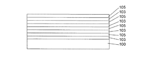
図1を参照すると、一実施形態では、基板100上に、第1の材料層103と、第2の材料層105とを有する多重層スタック101が形成される。後続の層は、第1の材料層103と第2の材料層105のこの交互パターンを繰り返すことができる。一実施形態では、第1の材料は酸化物とすることができ、第2の材料は窒化物とすることができる。他の実施形態では、第1/第2の材料スタックは酸化物/シリコン、シリコン/ドープされたシリコン、又はシリコン/窒化物とすることができる。これらの全ての材料の組み合わせを、ビットコストスケーラブル(BiCS)、テラビットセルアレイトランジスタ(TCAT)及び他の3Dメモリ構造体において用いることができる。他の実施形態では、第1/第2の材料スタックは他の材料の組み合わせとすることができる。基板上の第1の材料層及び第2の材料層の堆積順序は入れ替えることもできる。
Referring to FIG. 1, in one embodiment, a
層数は作製されるメモリデバイスによることができる。一実施形態では、スタック数は8X、又は16X、又は24X、又はそれ以上にすることができ、8、16、24又はそれ以上の層の各スタックが1つのメモリデバイスに対応する。異なる材料からなる2つの層が各スタックを形成するので、8xスタック数の場合の対応する層数は16とすることができ、16xスタック数の場合の対応する層数は32とすることができ、24xスタック数の場合の対応する層数は48とすることができ、それ以上のスタック数はそれ以上の層数を有することができる。 The number of layers can depend on the memory device being fabricated. In one embodiment, the number of stacks can be 8X, or 16X, or 24X, or more, with each stack of 8, 16, 24, or more layers corresponding to one memory device. Since two layers of different materials form each stack, the corresponding number of layers for an 8x stack number can be 16, and the corresponding number of layers for a 16x stack number can be 32. , The corresponding number of layers in the case of 24x stacks can be 48, and more stacks can have more layers.
図2を参照すると、PECVD処理チャンバ201が示される。処理チャンバ201は、ペデスタル211と、プロセスガスマニホールド213と、プロセスガス源215と、電極217と、交流RF電力を送出するRF電源219と、ヒータ221と、パージガス源221とを含む。一実施形態では、電極217はペデスタル211の上方に直接存在することができ、ペデスタルは容量性結合構成において電気的に接地される。一実施形態では、電極217は、プロセスガスのための流路を有するシャワーヘッド構造とすることができる。プロセスガス及びパージガスはマニホールド213及び電極217を通って、ペデスタルの上方のプロセスチャンバ201の中に流れ込むことができる。
Referring to FIG. 2, a
処理中に、基板100はペデスタル211上に配置され、PECVD処理チャンバ201に真空が印加される。ヒータ211にエネルギーを加えて、基板100を加熱することができる。第1のグループの処理ガスはマニホールド213を通って処理チャンバ201の中に進む。RF電源219によって電極217に電圧が印加され、電極217と接地されたペデスタル211との間に電界が生成される。一実施形態では、ペデスタル211は、可変高さ調整器上に存在することができ、それにより、基板100の上面と電極217との間の間隔を制御できるようにする。RF電界によって第1のグループのプロセスガスに電圧が印加され、プラズマ225が生成される。プラズマ225は十分なパーセンテージの原子又は分子を有し、それらの原子又は分子はイオン化され、電子を放出する。これらのエネルギー電子が前駆体分子の解離、及び大量の遊離基の生成を誘発することができる。この結果として、基板100上に材料が堆積される。所望の厚さの第1の材料が堆積されると、その堆積は中止することができる。第1の材料の層厚は100オングストローム〜1000オングストロームとすることができる。
During processing, the
基板100上に第1の材料が堆積された後に、PECVD処理チャンバ201はプラズマパージされる。パージガスがパージガス源221からマニホールド213及び処理チャンバ201の中に流れ込むことができる。電極217及びペデスタル211は、電圧を印加され、パージガスプラズマが生成される。NH3、N2、N2O、H3、Ar及び他の適切なプラズマパージガスを含む、種々のパージガスを用いることができる。パージプロセス中に、処理チャンバ内の熱及び圧力は保持することができる。プラズマパージは、更なる堆積のために露出した層の表面を調整する。調整済みの表面は結果として、層間の界面を滑らかにし、層間の接着を良好にし、さらには粒子制御を良好にする。幾つかの実施形態では、より良好な層結合を得るために粗い界面が望ましい場合があり、異なる、又は更なるプラズマパージプロセスを実行することができる。プラズマパージが完了した後に、電極217及びペデスタル211へのエネルギーをオフにすることができ、パージガス源222からのパージガスがマニホールド213及び処理チャンバ201の中に流れ込み、全てのガス汚染物質を除去する。一実施形態では、パージプロセス中に前駆体ガスのうちの1つ又は複数の成分が停止される。例えば、プロセスガスがSiH4及びN2Oの混合物を含む場合には、パージガスはN2Oのみを含むことができ、SiH4の流れは遮断される。他の実施形態では、1つ又は複数の異なるパージガスを用いることができる。
After the first material is deposited on the
プラズマパージ及びガスパージが完了した後に、基板上に第2の材料が堆積することができる。RF電源219によって電極217に電圧が印加され、電極217との間に電界が生成され、電界によって第2のグループのプロセスガスに電圧が印加され、プラズマ225が生成される。所望の厚さの第2の材料が堆積されると、その堆積は中止することができる。第2の材料の層厚は100オングストローム〜1000オングストロームとすることができる。第2の材料層が堆積された後に、上記のように、PECVDチャンバはプラズマパージすることができる。その後、電極217へのエネルギーを除去することができ、PECVDチャンバは上記のようにガスパージされる。プラズマパージ及びガスパージが完了すると、必要とされる層が堆積されるまで、第1の材料及び第2の材料を堆積するプロセスを繰り返すことができる。その後、更なる処理のために、PECVDチャンバ201から基板100を取り出すことができる。
After the plasma purge and gas purge are complete, a second material can be deposited on the substrate. A voltage is applied to the
同じPECVD処理チャンバ内で異なる材料の堆積が行われるので、上記の第1の材料及び第2の材料の層堆積プロセスは時間効率及びエネルギー効率が高い。第1の材料層及び第2の材料層を堆積する2つのPECVD処理チャンバ間でウエハが移送されないので、大幅に時間が節約される。例えば、開示されるプロセスの時間節約は、2つのPECVD処理チャンバを用いる同じ堆積プロセスよりも50%以上短時間にすることができる。また、単一のPECVD処理チャンバしか必要とされず、堆積される層毎に処理チャンバ内の真空を破壊し、再び真空を印加する必要がないので、上記の層スタック堆積プロセスはエネルギー効率が高い。 Since the deposition of different materials takes place in the same PECVD processing chamber, the layer deposition process of the first material and the second material described above is highly time and energy efficient. Significant time is saved because the wafer is not transferred between the two PECVD processing chambers that deposit the first material layer and the second material layer. For example, the time savings of the disclosed process can be over 50% shorter than the same deposition process using two PECVD processing chambers. Also, the layer stack deposition process described above is energy efficient because only a single PECVD process chamber is required and the vacuum in the process chamber need not be broken and reapplied again for each layer deposited. .
生じる可能性がある別の問題は、基板上に堆積された後に、異なる材料の堆積が圧縮応力又は引張応力を誘発する可能性があることである。この応力の結果として基板が曲がる可能性がある。図3を参照すると、基板100上に材料層291を堆積することができる。その際、第1の材料291は膨張し、圧縮応力295を引き起こす可能性がある。第1の材料層291の圧縮応力295に基板100が逆らって、基板100のエッジが弓状に下方に曲がる。同様に図4を参照すると、第2の材料層293を基板100上に堆積することができ、第2の材料293は引張応力297を誘発する場合がある。同じく、引張応力297に基板100が逆らう結果として、基板100のエッジが弓状に上方に曲がる。製造公差は非常に正確でなければならないので、基板にいくらかの曲がりがあるか、又は基板内にバンプがある結果として、後続のリソグラフィ処理が実行されるときに、アライメントの問題が生じる可能性がある。このアライメント不良の結果として、製造誤差が生じ、欠陥のあるデバイスが構成される可能性がある。
Another problem that may arise is that the deposition of different materials can induce compressive or tensile stress after being deposited on the substrate. As a result of this stress, the substrate can bend. Referring to FIG. 3, a
この問題を解消するために、一実施形態では、堆積される各層によって基板に加えられる応力を調整することができる。応力は堆積される材料によることができる。また、応力は、プロセス温度、前駆体ガスの流量、ガス圧及びプラズマ密度を含む堆積処理条件を調整することによって限られた範囲内で調整することができる。例えば、処理温度が低いと圧縮応力を生成することができ、処理温度が高いと引張応力を生成することができる。プラズマ圧が低いと、反応種へのイオン衝撃を大きくすることができ、それゆえ、結果として圧縮応力が生じ、逆にプラズマ圧が高い結果として、引張応力が生じる可能性がある。RF電力を高めるか、又は基板上方の間隔を小さくすることによってプラズマ密度を高めることができ、それにより反応種へのイオン衝撃を大きくすることができ、それゆえ、結果として圧縮応力を生成することができ、プラズマ密度が低い結果として、引張応力を生成することができる。温度及びプラズマ密度を制御することによって、堆積される材料の応力を予測することができる。 To overcome this problem, in one embodiment, the stress applied to the substrate by each deposited layer can be adjusted. The stress can depend on the material being deposited. Also, the stress can be adjusted within a limited range by adjusting the deposition process conditions including process temperature, precursor gas flow rate, gas pressure and plasma density. For example, a compressive stress can be generated when the processing temperature is low, and a tensile stress can be generated when the processing temperature is high. If the plasma pressure is low, ion bombardment to the reactive species can be increased, thus resulting in compressive stress and conversely high plasma pressure can result in tensile stress. The plasma density can be increased by increasing the RF power, or by reducing the spacing above the substrate, thereby increasing the ion bombardment to the reactive species and thus creating compressive stress As a result of the low plasma density, tensile stress can be generated. By controlling the temperature and plasma density, the stress of the deposited material can be predicted.
図5を参照すると、多層スタック101の断面が示されており、図6は多層スタック101の平面図を示す。第1の材料層291の引張応力295は、第1の材料層291上に堆積される第2の材料層293の圧縮応力297に概ね等しくすることができる。これらの応力295、297は逆向きであるので、それらの応力は実質的に相殺する。等しい数の引張層及び圧縮層があるので、基板100にかかる全正味応力は0に近い。
Referring to FIG. 5, a cross section of the
例えば、第1の材料層291は圧縮応力を生成する酸化シリコンとすることができる。第2の層293は引張応力を生成する窒化シリコン層とすることができる。窒化シリコンからなる第2の層293によって生成される引張応力の大きさは、酸化シリコンからなる第1の層291の圧縮応力に概ね等しくすることができる。これらの層対291、293は重ねて堆積され、結果として、150MPa未満の低い全正味応力を有する、応力の均衡が保たれた層スタック101が形成される。この結果として、基板100には、堆積された層の応力に起因する歪み変形は生じない。応力の均衡が保たれているので、変形は最小限に抑えられ、基板100の上面は平滑である。層291及び293が堆積された後に正確なリソグラフィ処理を実行して、BiSC3Dメモリのような半導体デバイスを形成するために、平坦な基板表面が必要とされる。弓状に曲がるか、又は別の態様で変形する基板100は、結果としてリソグラフィ誤差を生じることになる。
For example, the
先に論じられたように、種々の組み合わせの材料を基板100上に層として堆積することができる。これらの材料はそれぞれ、特定のプロセスガス及び特定のPECVD動作条件を用いて堆積することができる。層スタックを堆積するためのプロセスは図7〜図10において示されており、それらの図は、基板上の複数の層内に異なる組み合わせの材料を堆積するために用いることができる堆積プロセスのための流れ図である。
As discussed above, various combinations of materials can be deposited as layers on the
図7を参照すると、基板上に酸化シリコン及び窒化シリコンの層スタックをイン・サイチュ堆積するための流れ図が示される。PECVD処理チャンバ内に基板が配置され、チャンバに真空が印加される(301)。チャンバ内の真空圧は約0.5Torr〜10Torrとすることができる。処理チャンバは約180℃〜650℃に加熱される。電極に加えられる高周波又はRF電力は約45ワット(W)〜1000Wとすることができ、基板と電極との間の間隔は約200mil〜800milとすることができる。第1のプロセスガスはSiH4及びN2O又は他のシリコン含有分子及び酸素含有分子を含むことができる。SiH4は、約20標準立方センチメートル/分(sccm)〜1,000sccmの流量とすることができ、N2Oの流量は約1,000sccm〜20,000sccmとすることができる。SiH4及びN2Oは活性化され、Siイオン及びOイオンを含むプラズマに変換される。イオンの反応によって、基板上に酸化シリコンの層が堆積される(303)。その堆積は、必要とされる酸化シリコン厚が堆積された後に中止される。 Referring to FIG. 7, a flow diagram for in-situ deposition of a silicon oxide and silicon nitride layer stack on a substrate is shown. A substrate is placed in the PECVD processing chamber and a vacuum is applied to the chamber (301). The vacuum pressure in the chamber can be about 0.5 Torr to 10 Torr. The processing chamber is heated to about 180 ° C to 650 ° C. The high frequency or RF power applied to the electrodes can be about 45 watts (W) to 1000 W, and the spacing between the substrate and the electrodes can be about 200 mils to 800 mils. The first process gas can include SiH 4 and N 2 O or other silicon-containing molecules and oxygen-containing molecules. SiH 4 can have a flow rate of about 20 standard cubic centimeters per minute (sccm) to 1,000 sccm, and N 2 O can have a flow rate of about 1,000 sccm to 20,000 sccm. SiH 4 and N 2 O are activated and converted to a plasma containing Si ions and O ions. A layer of silicon oxide is deposited on the substrate by the reaction of ions (303). The deposition is stopped after the required silicon oxide thickness is deposited.
一実施形態では、SiH4を処理チャンバに導入する前にプラズマをオンに切り替えることによって酸化シリコン表面上の表面粗さを低減することができる。SiH4種の滞留時間を短縮することによって、ウエハ表面が更に滑らかになり、それにより、堆積される後続の層との界面結合を改善することができる。 In one embodiment, the surface roughness on the silicon oxide surface can be reduced by switching on the plasma before introducing SiH 4 into the processing chamber. By shortening the residence time of the SiH 4 species, the wafer surface can be made even smoother, thereby improving interfacial bonding with subsequent deposited layers.
酸化シリコンが堆積された後に、PECVD処理チャンバはプラズマパージ及びガスパージされる。その温度は約180℃〜650℃とすることができ、真空圧は約0.5Torr〜10Torrとすることができる。基板と電極との間の間隔は約200mil〜800milとすることができる。N2Oのパージガスは、マニホールドを通って約2,000sccm〜30,000sccmの流量において処理チャンバに流れ込むことができる(305)。電極及びペデスタルに電圧を印加し、100W〜1,000Wの電力を有するパージガスプラズマを生成する。プラズマパージ及びN2Oパージは処理チャンバを洗浄し、結果として、層間の界面を滑らかにし、堆積された層間の接着を良好にし、さらには粒子制御を良好にする。 After the silicon oxide is deposited, the PECVD process chamber is plasma purged and gas purged. The temperature can be about 180 ° C. to 650 ° C., and the vacuum pressure can be about 0.5 Torr to 10 Torr. The spacing between the substrate and the electrode can be about 200 mil to 800 mil. Purge N 2 O can flow into the processing chamber at a flow rate of about 2,000sccm~30,000sccm through the manifold (305). A voltage is applied to the electrode and the pedestal to generate a purge gas plasma having a power of 100 W to 1,000 W. The plasma purge and N 2 O purge clean the processing chamber, resulting in a smooth interface between layers, good adhesion between deposited layers, and better particle control.
パージが完了した後に、酸化シリコン層上に窒化シリコンの層を堆積することができる。チャンバ内の圧力は約0.5Torr〜10Torrとすることができる。処理チャンバは約180℃〜650℃に加熱される。電極に加えられる高周波又はRF電力は約50W〜700Wとすることができ、基板と電極との間の間隔は約200mil〜800milとすることができる。第2のプロセスガスはSiH4、NH3及びN2又は他のシリコン含有分子及び窒素含有分子を含むことができる。SiH4は、約20sccm〜1,000sccmの流量を有することができ、NH3の流量は約50sccm〜1,000sccmとすることができ、N2の流量は約2,000sccm〜30,000sccmとすることができる。SiH4、NH3及びN2は活性化され、Siイオン及びNイオンを含むプラズマに変換され、それらのイオンが反応して、基板上に窒化シリコンの層を堆積する(307)。その堆積は、必要とされる窒化シリコン厚が堆積された後に中止される。その後、システムは、更なる層が堆積される必要があると判断する(309)。 After the purge is complete, a layer of silicon nitride can be deposited on the silicon oxide layer. The pressure in the chamber can be about 0.5 Torr to 10 Torr. The processing chamber is heated to about 180 ° C to 650 ° C. The high frequency or RF power applied to the electrodes can be about 50 W to 700 W, and the spacing between the substrate and the electrodes can be about 200 mils to 800 mils. The second process gas can include SiH 4 , NH 3 and N 2 or other silicon-containing molecules and nitrogen-containing molecules. SiH 4 may have a flow rate of about 20 sccm to 1,000 sccm, NH 3 may have a flow rate of about 50 sccm to 1,000 sccm, and N 2 may have a flow rate of about 2,000 sccm to 30,000 sccm. be able to. SiH 4 , NH 3 and N 2 are activated and converted to a plasma containing Si and N ions, which react to deposit a layer of silicon nitride on the substrate (307). The deposition is stopped after the required silicon nitride thickness is deposited. Thereafter, the system determines (309) that additional layers need to be deposited.
窒化シリコンが堆積された後に、窒化シリコン層311上でプラズマ処理を実行して、窒化シリコン上に酸化シリコン層を確実に堆積できるように窒化シリコン上の結合界面表面を改善することができる。基板の正味応力は0に近くすることができるが、隣接する任意の層間の界面結合が弱い場合には、隣接する層間の個々の応力によって層間剥離が生じる恐れがある。層スタックの単一の部分に層間剥離がある結果として、デバイスに欠陥が生じることになる。したがって、層間剥離を防ぐために、隣接する層間に強い界面結合が必要とされる。一実施形態では、窒化シリコン層上に堆積される材料との強い結合が生じるように、窒化シリコン層上で実行されるプラズマ処理によって、表面粗さを改善することもできる。
After the silicon nitride is deposited, a plasma treatment can be performed on the
隣接する層間の界面結合が強く、かつ層の応力が、大きさが等しく、方向が逆である場合には、基板上の正味応力は150MPa未満とすることができ、基板は層内の応力によって変形しない。基板が変形しないので、層スタックが堆積された後に、上面は平滑になる。酸化物層及び窒化物層が堆積された後に正確なリソグラフィ処理を実行して、BiSC及びTCAT3Dメモリのような半導体デバイスを形成するために、滑らかな表面が必要とされる。層スタック101の上面内のバンプ又は曲がりがある結果として、リソグラフィ誤差が生じ、それにより、作製されるディスプレイ内に欠陥が生じる可能性がある。
If the interfacial bond between adjacent layers is strong and the stresses in the layers are equal in magnitude and reversed, the net stress on the substrate can be less than 150 MPa, and the substrate can Does not deform. Since the substrate does not deform, the top surface becomes smooth after the layer stack is deposited. A smooth surface is required to perform accurate lithographic processing after oxide and nitride layers are deposited to form semiconductor devices such as BiSC and TCAT3D memories. As a result of bumps or bends in the top surface of the
一実施形態では、プラズマ処理ガスはNH3及びN2を含むことができる。処理チャンバは約180℃〜650℃に加熱され、真空圧は約0.5Torr〜10Torrとすることができる。電極に加えられる高周波又はRF電力は約200W〜2000Wとすることができ、基板と電極との間の間隔は約200mil〜800milとすることができる。NH3は約50sccm〜1,000sccmの流量を有することができ、N2の流量は約2,000sccm〜30,000sccmとすることができる。NH3及びN2は活性化されてプラズマになり、そのプラズマが窒化シリコン層の表面を処理し、必要とされる表面粗さを与えることによって界面を改善する。調整済み表面は、堆積されることになる酸化シリコン層との良好な界面結合を与える。層間の強い結合は層間剥離を防ぎ、基板の曲がり又は変形を防ぐ。 In one embodiment, the plasma processing gas can include NH 3 and N 2 . The processing chamber is heated to about 180 ° C. to 650 ° C., and the vacuum pressure can be about 0.5 Torr to 10 Torr. The high frequency or RF power applied to the electrodes can be about 200 W to 2000 W, and the spacing between the substrate and the electrodes can be about 200 mils to 800 mils. NH 3 can have a flow rate between about 50 sccm and 1,000 sccm, and the flow rate of N 2 can be between about 2,000 sccm and 30,000 sccm. NH 3 and N 2 are activated into a plasma that improves the interface by treating the surface of the silicon nitride layer and providing the required surface roughness. The conditioned surface provides good interfacial bonding with the silicon oxide layer to be deposited. Strong bonding between layers prevents delamination and prevents substrate bending or deformation.
窒化シリコンプラズマ処理が実行された後に、処理チャンバはパージされる(313)。ステップ313のパージプロセスは、上記のステップ305を参照しながら行った先の説明と同じプロセスにすることができ、約2,000sccm〜約30,000sccmの流量においてN2パージガスを用いる。その後、基板上に必要とされる数の酸化物層及び窒化物層が堆積されるまで(309)、プロセスステップ303〜313を繰り返すことができる。
After the silicon nitride plasma process is performed, the process chamber is purged (313). The purge process of
3Dメモリデバイスでは、上記のようにして堆積される層の数は、垂直に積重されるメモリトランジスタの数に比例する。一実施形態では、基板上に、8、16、24又はそれ以上のトランジスタを垂直に配置することができる。各トランジスタは、一対の隣接する層を必要とする場合がある。したがって、必要とされる層数は16、32、48又はそれ以上とすることができる。必要とされる材料層が基板上に堆積された後に、PECVD処理チャンバは周囲圧に戻され、更なる処理を実行できるように、PECVDチャンバから基板が取り出される(315)。 In 3D memory devices, the number of layers deposited as described above is proportional to the number of memory transistors stacked vertically. In one embodiment, 8, 16, 24, or more transistors can be placed vertically on a substrate. Each transistor may require a pair of adjacent layers. Thus, the required number of layers can be 16, 32, 48 or more. After the required material layer is deposited on the substrate, the PECVD processing chamber is returned to ambient pressure and the substrate is removed from the PECVD chamber so that further processing can be performed (315).
図8を参照すると、基板上の酸化シリコン及びシリコンの層スタックのイン・サイチュ堆積のための流れ図が示される。PECVD処理チャンバ内に基板が配置され、チャンバに真空が印加される(401)。酸化シリコン材料は、上記の図7のステップ303を参照しながら行った先の説明と同じようにして、同じ動作条件で堆積することができる。プロセスガスを活性化し、Siイオン及びOイオンを含むプラズマに変換することができ、それらのイオンは反応して、基板上に酸化シリコンの層が堆積される(403)。酸化シリコンが堆積された後に、チャンバはプラズマパージ及びガスパージされる(405)。図7のステップ305において先に説明されたのと同じパージプロセスを用いることができる。
Referring to FIG. 8, a flow diagram for in situ deposition of a silicon oxide and silicon layer stack on a substrate is shown. A substrate is placed in the PECVD processing chamber and a vacuum is applied to the chamber (401). The silicon oxide material can be deposited under the same operating conditions in the same manner as described above with reference to step 303 of FIG. 7 above. The process gas can be activated and converted to a plasma containing Si and O ions, which react to deposit a layer of silicon oxide on the substrate (403). After the silicon oxide is deposited, the chamber is plasma purged and gas purged (405). The same purge process previously described in
処理チャンバがプラズマパージ及びガスパージされた後に、酸化シリコン層上にシリコン層を堆積することができる(407)。チャンバ内の圧力は約0.5Torr〜10Torrとすることができる。処理チャンバは約400℃〜650℃に加熱される。電極に加えられる高周波又はRF電力は約50W〜700Wとすることができ、基板と電極との間の間隔は約200mil〜800milとすることができる。プロセスガスはSiH4又は他のシリコン含有分子及びHeを含むことができる。SiH4は、約50sccm〜2,000sccmの流量を有することができ、Heの流量は約1,000sccm〜20,000sccmとすることができる。プロセスガスを活性化して、シリコンイオンを形成し、それらのイオンは電子と反応して、シリコン層を堆積する。システムは更なる層が必要であると判断し(409)、更なる堆積に備えて、PECVDチャンバをパージすることができる(415)。全ての酸化シリコン層及びシリコン層が堆積されるまで、プロセスステップ403〜411を繰り返すことができる。層が堆積された後に(409)、PECVDチャンバが周囲圧に戻され、基板が取り出される(415)。3Dメモリの場合、基板上に、少なくとも8つの材料層が堆積されなければならない。他の処理チャンバにおいて更なる処理を実行することができる。 After the processing chamber has been plasma purged and gas purged, a silicon layer may be deposited on the silicon oxide layer (407). The pressure in the chamber can be about 0.5 Torr to 10 Torr. The processing chamber is heated to about 400 ° C to 650 ° C. The high frequency or RF power applied to the electrodes can be about 50 W to 700 W, and the spacing between the substrate and the electrodes can be about 200 mils to 800 mils. The process gas can include SiH 4 or other silicon-containing molecules and He. SiH 4 can have a flow rate between about 50 sccm and 2,000 sccm, and the flow rate of He can be between about 1,000 sccm and 20,000 sccm. The process gas is activated to form silicon ions that react with electrons to deposit a silicon layer. The system determines that additional layers are needed (409) and can purge the PECVD chamber (415) in preparation for further deposition. Process steps 403-411 can be repeated until all silicon oxide and silicon layers are deposited. After the layer is deposited (409), the PECVD chamber is returned to ambient pressure and the substrate is removed (415). For 3D memory, at least eight material layers must be deposited on the substrate. Further processing can be performed in other processing chambers.
図9を参照すると、一実施形態では、基板上にシリコン及びドープされたシリコンの層スタックを堆積することができる。PECVD処理チャンバ内に基板が配置され、チャンバに真空が印加される(501)。基板上にシリコン材料が堆積される(503)。図8のステップ403を参照しながら先に説明されたシリコン堆積プロセスを用いてシリコン層を堆積することができる。シリコン材料が堆積された後に、処理チャンバはプラズマパージ及びガスパージされる(505)。図7のステップ305において先に説明されたパージプロセスを用いてPECVDチャンバをパージすることができる。
Referring to FIG. 9, in one embodiment, a layer stack of silicon and doped silicon can be deposited on a substrate. A substrate is placed in the PECVD processing chamber and a vacuum is applied to the chamber (501). A silicon material is deposited on the substrate (503). The silicon layer can be deposited using the silicon deposition process described above with reference to step 403 of FIG. After the silicon material is deposited, the process chamber is plasma purged and gas purged (505). The PECVD chamber can be purged using the purge process previously described in
その後、シリコン及びドーパント前駆体の両方を処理チャンバに送り込むことによって、シリコン層上にドープされたシリコン材料を堆積することができる(507)。ドープされたシリコンは、シリコンと、シリコンの導電率を高める不純物とを含む。導電率は、不純物原子の数によってだけではなく、不純物原子のタイプによっても変更することができる。ドープされたシリコンの堆積処理は、上記の図8のステップ407において先に説明されたシリコン堆積に類似している。プロセスガスはSiH4及びHe、並びにp型又はn型にドープされたシリコン層を作り出す他のドーパントガスを含むことができる。ドーパント前駆体ガスをSiH4及びH2と混合し、堆積したシリコン結晶格子に更に不純物を添加する。 Thereafter, doped silicon material may be deposited on the silicon layer by feeding both silicon and a dopant precursor into the processing chamber (507). Doped silicon includes silicon and impurities that increase the conductivity of the silicon. The conductivity can be changed not only by the number of impurity atoms but also by the type of impurity atoms. The doped silicon deposition process is similar to the silicon deposition previously described in step 407 of FIG. 8 above. The process gas can include SiH 4 and He, and other dopant gases that create a p-type or n-type doped silicon layer. The dopant precursor gas is mixed with SiH 4 and H 2 and further impurities are added to the deposited silicon crystal lattice.
p型にドープされたシリコンを生成するために、Bドーパント前駆体ガスが必要とされる。適切なドーパント前駆体ガスは、B(CH3)3トリメチルホウ素TMB及びB2H6ジボラン又は他のホウ素含有分子を含み、それらのガスはSiH4及びHeとともに処理チャンバに流れ込むことができる。他の実施形態では、ホウ素を含む他の処理ガスを用いることができる。p型ドーパントガスをSiH4及びHeと混合し、堆積したシリコン結晶格子に更に不純物を添加する。これらのBドーパント前駆体ガスは約1sccm〜50sccmの流量を有することができる。Bドーパント前駆体ガスの流量は、p型にドープされたシリコン層内のBドーパントの濃度に比例することができる。必要とされるp型シリコン厚が堆積された後に、その堆積は中止される。一実施形態では、p型にドープされたシリコン層からホウ素が拡散する場合がある。ホウ素拡散を最小限に抑えるために、薄い窒素リッチ材料層をp型にドープされたシリコン層に隣接して堆積することができる。窒素リッチ材料は、必要とされる量のホウ素がドープされたシリコン内にとどまるように、ドープされたシリコン層からホウ素が拡散するのを防ぐことができる。 A B dopant precursor gas is required to produce p-type doped silicon. Suitable dopant precursor gases include B (CH 3 ) 3 trimethylboron TMB and B 2 H 6 diborane or other boron containing molecules that can flow into the processing chamber along with SiH 4 and He. In other embodiments, other process gases including boron can be used. A p-type dopant gas is mixed with SiH 4 and He, and further impurities are added to the deposited silicon crystal lattice. These B dopant precursor gases can have a flow rate between about 1 sccm and 50 sccm. The flow rate of the B dopant precursor gas can be proportional to the concentration of the B dopant in the p-type doped silicon layer. After the required p-type silicon thickness is deposited, the deposition is stopped. In one embodiment, boron may diffuse from a p-type doped silicon layer. In order to minimize boron diffusion, a thin nitrogen-rich material layer can be deposited adjacent to the p-type doped silicon layer. The nitrogen-rich material can prevent boron from diffusing from the doped silicon layer so that the required amount of boron remains in the doped silicon.
n型にドープされたシリコンを生成するために、Pドーパント前駆体ガスが必要とされる。適切なPドーパント前駆体ガスは、PH3ホスフィン及び他のリン含有分子を含み、それらのガスは、約1sccm〜50sccmの流量でSiH4及びHeとともに処理チャンバに流れ込むことができる。他の実施形態では、他のリン含有分子を用いることができる。PH3の流量は、n型にドープされたシリコン層内のPドーパントの濃度に比例することができる。必要とされるn型シリコン厚が堆積された後に、その堆積処理は中止される。 A P dopant precursor gas is required to produce n-type doped silicon. Suitable P dopant precursor gases include PH 3 phosphine and other phosphorus-containing molecules that can flow into the processing chamber with SiH 4 and He at a flow rate between about 1 sccm and 50 sccm. In other embodiments, other phosphorus-containing molecules can be used. The flow rate of PH 3 can be proportional to the concentration of P dopant in the n-type doped silicon layer. After the required n-type silicon thickness is deposited, the deposition process is stopped.
ドープされたシリコンが堆積された後に、そのシステムは更なる層が必要である判断することができ(509)、PECVD処理チャンバをパージすることができ(511)、必要とされる層が堆積されるまで(509)、ステップ503〜511を繰り返すことができ、その数は4層以上とすることができる。全ての層が同じPECVD処理チャンバ内で堆積され、層の堆積全体を通して処理チャンバ内の真空が保持される。シリコン及びドープされたシリコン層が堆積された後に、PECVD処理チャンバの真空を解除することができ、基板を取り出すことができる(515)。その後、ウエハにおいて更なる処理を実行することができる。 After the doped silicon is deposited, the system can determine that additional layers are needed (509) and can purge the PECVD processing chamber (511), and the required layers are deposited. (509), steps 503 to 511 can be repeated, and the number can be four or more. All layers are deposited in the same PECVD processing chamber and the vacuum in the processing chamber is maintained throughout the deposition of the layers. After the silicon and doped silicon layers are deposited, the PECVD process chamber vacuum can be released and the substrate can be removed (515). Thereafter, further processing can be performed on the wafer.
別の実施形態では、異なるプロセスを用いて、ウエハ上にシリコン及びドープされたシリコンの層スタックを堆積することができる。ドーパント前駆体の流量のオン/オフを切り替えることによって、シリコンプラズマ及びドープされたシリコンプラズマを次々に流し込むことができる。図10を参照すると、PECVD処理チャンバ内に基板が配置され、チャンバが真空にされる(501)。電極にPR電力が加えられる。シリコン前駆体ガスが処理チャンバに流れ込み、プラズマを生成し、図9に関して先に説明されたようにウエハ上にシリコンの層が堆積される。必要とされるシリコン厚が堆積された後に、ドープされたシリコンが堆積される。プラズマパージ及びガスパージを実行するのではなく、シリコン前駆体にドーパント前駆体が加えられ(506)、シリコン層上にドープされたシリコンが堆積される(507)。必要とされるドープされたシリコン厚が堆積されたとき、ドーパント前駆体が停止され(512)、ウエハ上に更なるシリコン層が堆積される(503)。全てのシリコン/ドープされたシリコン層が堆積されるまで(509)、プロセスステップ503〜512が繰り返される。シリコン及びドープされたシリコン層が堆積された後に、PECVD処理チャンバの真空を解除することができ、基板を取り出すことができ(515)、その後、ウエハにおいて更なる処理を実行することができる。プラズマパージ及びガスパージステップが不要であるので、上記のようなウエハのシリコン/ドープされたシリコン層スタック堆積処理は、はるかに効率的にすることができる。 In another embodiment, a different process can be used to deposit a layer stack of silicon and doped silicon on the wafer. By switching on / off the flow rate of the dopant precursor, silicon plasma and doped silicon plasma can be flowed one after another. Referring to FIG. 10, a substrate is placed in a PECVD processing chamber and the chamber is evacuated (501). PR power is applied to the electrodes. A silicon precursor gas flows into the processing chamber and generates a plasma, and a layer of silicon is deposited on the wafer as previously described with respect to FIG. After the required silicon thickness is deposited, doped silicon is deposited. Rather than performing a plasma purge and gas purge, a dopant precursor is added to the silicon precursor (506), and doped silicon is deposited on the silicon layer (507). When the required doped silicon thickness is deposited, the dopant precursor is stopped (512) and an additional silicon layer is deposited on the wafer (503). Process steps 503-512 are repeated until all silicon / doped silicon layers have been deposited (509). After the silicon and doped silicon layers are deposited, the PECVD process chamber vacuum can be released, the substrate can be removed (515), and further processing can then be performed on the wafer. Since the plasma purge and gas purge steps are not necessary, the silicon / doped silicon layer stack deposition process of the wafer as described above can be made much more efficient.
一実施形態では、シリコン及びドープされたシリコン層の水素含有量を削減することが望ましい場合がある。水素含有量を削減することによって、ウエハの後続のアニーリング処理中のガス発生を低減することができる。また、水素含有量が少ないと、層スタック、又は炭素系膜、金属窒化物及び誘電体窒化物を含むことができるハードマスク構造の界面における層間剥離を防ぐこともできる。 In one embodiment, it may be desirable to reduce the hydrogen content of silicon and doped silicon layers. By reducing the hydrogen content, gas evolution during subsequent annealing of the wafer can be reduced. A low hydrogen content can also prevent delamination at the interface of the layer stack or hard mask structure that can include carbon-based films, metal nitrides and dielectric nitrides.
図11を参照すると、一実施形態では、基板上にシリコン及びドープされたシリコンの層スタックを堆積することができる。PECVD処理チャンバ内に基板が配置され、真空にされる(801)。基板上にシリコン材料が堆積される(803)。図8のステップ403を参照しながら先に説明されたシリコン堆積プロセスを用いて、シリコン層を堆積することができる。シリコン材料が堆積された後に、処理チャンバをパージすることができる(805)。図7のステップ305において先に説明されたパージプロセスを用いて、PECVDチャンバをパージすることができる。
Referring to FIG. 11, in one embodiment, a layer stack of silicon and doped silicon can be deposited on a substrate. The substrate is placed in a PECVD processing chamber and evacuated (801). A silicon material is deposited on the substrate (803). The silicon layer can be deposited using the silicon deposition process described above with reference to step 403 of FIG. After the silicon material is deposited, the processing chamber can be purged (805). The PECVD chamber can be purged using the purge process previously described in
シリコン層上に窒化シリコン層を直接堆積するのではなく、電極にRF電力を加えながらPECVD処理チャンバの中に酸化シリコンプロセスガスを導入することによって、シリコン層上に薄い酸化シリコン層を堆積することができる(807)。酸化シリコンは、シリコン層と窒化シリコン層との間の結合を改善し、後続のアニーリングプロセス中の界面における層間剥離を防ぐ接着剤としての役割を果たすことができる。シリコン層上に酸化シリコンの薄膜が堆積される。酸化シリコン堆積プロセスは図7のステップ303を参照しながら説明される。その後、チャンバをプラズマパージ及びガスパージすることができ(809)、酸化シリコン層上に窒化シリコン層が堆積される(811)。界面が改善されるように、窒化シリコン上で窒化シリコン処理を実行して表面粗さを改善することができ(815)、プラズマパージ及びガスパージ(817)プロセスを繰り返すことができる。一実施形態では、ステップ807、809、811、815及び817は、図7のステップ303、305、307、311及び313を参照しながらそれぞれ説明される。
Rather than depositing a silicon nitride layer directly on the silicon layer, a thin silicon oxide layer is deposited on the silicon layer by introducing a silicon oxide process gas into the PECVD processing chamber while applying RF power to the electrodes. (807). The silicon oxide can serve as an adhesive that improves the bond between the silicon layer and the silicon nitride layer and prevents delamination at the interface during the subsequent annealing process. A thin film of silicon oxide is deposited on the silicon layer. The silicon oxide deposition process is described with reference to step 303 of FIG. The chamber can then be plasma purged and gas purged (809), and a silicon nitride layer is deposited over the silicon oxide layer (811). To improve the interface, a silicon nitride process can be performed on the silicon nitride to improve surface roughness (815), and the plasma and gas purge (817) processes can be repeated. In one embodiment, steps 807, 809, 811, 815 and 817 are described with reference to
材料堆積は様々に組み合わせることができる。以下の表1を参照すると、層スタックのために取り得る第1の材料及び第2の材料が掲載される。第1の材料層及び第2の材料層の堆積順は、応用形態の要件に応じて変更することができる、すなわち、逆にすることができる。

図12を参照すると、基板上に第1の材料及び第2の材料の層スタックをイン・サイチュ堆積するための流れ図が示される。PECVDチャンバ内に基板が配置され(601)、基板上に第1の材料が堆積される(603)。PECVDチャンバがプラズマパージ及びガスパージされる(605)。必要な場合には、第1の材料層上でプラズマ処理を実行することができる(606)。第1の材料上に第2の材料が堆積される(607)。基板上に更なる層が堆積される(609)。必要な場合には、第2の材料層上でプラズマ処理を実行することができる(611)。PECVDチャンバが再びパージされ(613)、プロセスステップ603〜613を繰り返して、基板上に更なる層を堆積する。全ての層が堆積された後に、PECVDチャンバは周囲圧に戻され、基板が取り出される(615)。更なるエッチング及び堆積プロセスを実行して、基板上に3Dメモリデバイスを作り出すことができる。 Referring to FIG. 12, a flow diagram for in-situ deposition of a layer stack of a first material and a second material on a substrate is shown. A substrate is placed in the PECVD chamber (601), and a first material is deposited on the substrate (603). The PECVD chamber is plasma purged and gas purged (605). If necessary, a plasma treatment can be performed on the first material layer (606). A second material is deposited on the first material (607). A further layer is deposited on the substrate (609). If necessary, a plasma treatment can be performed on the second material layer (611). The PECVD chamber is purged again (613) and process steps 603-613 are repeated to deposit additional layers on the substrate. After all layers are deposited, the PECVD chamber is returned to ambient pressure and the substrate is removed (615). Further etching and deposition processes can be performed to create 3D memory devices on the substrate.
本発明のシステムが特定の実施形態を参照しながら説明されてきたが、本発明のシステムの範囲から逸脱することなく、これらの実施形態に付加、削除及び変更を加えることができることは理解されよう。説明されてきたシステムは種々の構成要素を含むが、これらの構成要素及び説明された構成は変更することができ、種々の他の構成において構成し直すことができることを十分に理解されたい。 Although the system of the present invention has been described with reference to particular embodiments, it will be understood that additions, deletions and modifications may be made to these embodiments without departing from the scope of the present system. . Although the system that has been described includes various components, it should be appreciated that these components and the described configuration can be varied and reconfigured in various other configurations.
Claims (16)
(b)第1のプロセスガスを第1のプラズマに活性化するステップと、
(c)前記第1のプラズマから前記基板上に第1の方向に第1の応力を有する第1の材料の層を堆積するステップと、
(d)前記PECVDチャンバをプラズマパージし、前記プラズマパージによって堆積のために調整されるように前記第1の材料の表面を暴露するステップと、
(e)前記PECVDチャンバをガスパージして全てのガス汚染物質を除去するステップと、
(f)第2のプロセスガスを第2のプラズマに活性化するステップと、
(g)前記第2のプラズマから前記基板上に、前記第1の方向と逆の第2の方向に第2の応力を有する第2の材料の層を堆積するステップと、
(h)前記PECVDチャンバをプラズマパージし、前記プラズマパージによって堆積のために調整されるように前記第2の材料の表面を暴露するステップと、
(i)前記PECVDチャンバをガスパージしてガス汚染物質を除去するステップと、
(j)ステップ(b)〜(i)全体を通して前記PECVDチャンバ内の真空を保持するステップと、
(k)前記基板上に所定の数の前記第1の材料の層及び前記第2の材料の層が堆積され、且つ前記基板の上面が平滑となるまで、ステップ(b)〜(j)を繰り返すステップとを含む、方法。 (A) placing a substrate in a PECVD chamber;
(B) activating a first process gas to a first plasma;
(C) depositing a layer of a first material having a first stress in a first direction on the substrate from the first plasma;
(D) plasma purging the PECVD chamber and exposing the surface of the first material to be conditioned for deposition by the plasma purge;
(E) purging the PECVD chamber to remove all gas contaminants;
(F) activating a second process gas to a second plasma;
(G) depositing a layer of a second material having a second stress in a second direction opposite to the first direction on the substrate from the second plasma;
(H) plasma purging the PECVD chamber and exposing the surface of the second material to be conditioned for deposition by the plasma purge;
(I) gas purging the PECVD chamber to remove gas contaminants;
(J) maintaining a vacuum in the PECVD chamber throughout steps (b)-(i);
(K) Steps (b)-(j) until a predetermined number of layers of the first material and second material are deposited on the substrate and the top surface of the substrate is smooth. Repeating the method.
(b)第1のプロセスガスを第1のプラズマに活性化するステップと、
(c)前記第1のプラズマから前記基板上に第1の方向に第1の応力を有する第1の材料の層を堆積するステップと、
(d)プラズマパージして前記PECVDチャンバを洗浄し、堆積のために調整されるように前記第1の材料の表面を暴露するステップと、
(e)前記PECVDチャンバをガスパージしてガス汚染物質を除去するステップと、
(f)第2のプロセスガスを第2のプラズマに活性化するステップと、
(g)前記基板上に、前記第1の材料の前記第1の方向の前記第1の応力と大きさが概ね等しく、かつ方向が逆である第2の方向の第2の応力を有する第2の材料の層を堆積するステップと、
(h)前記PECVDチャンバをプラズマパージし、堆積のために調整されるように前記第2の材料の表面を暴露するステップと、
(i)前記PECVDチャンバをガスパージしてガス汚染物質を除去するステップと、
(j)ステップ(b)〜(i)全体を通して前記PECVDチャンバ内の真空を保持するステップと、
(k)前記基板上に所定の数の前記第1の材料の層及び前記第2の材料の層が堆積され、且つ前記基板の上面が平滑となるまで、ステップ(b)〜(j)を繰り返すステップとを含む、方法。 (A) placing the substrate in a PECVD chamber in a vacuum;
(B) activating a first process gas to a first plasma;
(C) depositing a layer of a first material having a first stress in a first direction on the substrate from the first plasma;
(D) plasma purging to clean the PECVD chamber and exposing the surface of the first material to be conditioned for deposition;
(E) purging the PECVD chamber to remove gas contaminants;
(F) activating a second process gas to a second plasma;
(G) a second stress on the substrate having a second stress in a second direction that is approximately equal in magnitude and opposite to the first stress in the first direction of the first material; Depositing a layer of two materials;
(H) plasma purging the PECVD chamber and exposing the surface of the second material to be conditioned for deposition;
(I) gas purging the PECVD chamber to remove gas contaminants;
(J) maintaining a vacuum in the PECVD chamber throughout steps (b)-(i);
(K) Steps (b)-(j) until a predetermined number of layers of the first material and second material are deposited on the substrate and the top surface of the substrate is smooth. Repeating the method.
Applications Claiming Priority (3)
| Application Number | Priority Date | Filing Date | Title |
|---|---|---|---|
| US12/899,401 | 2010-10-06 | ||
| US12/899,401 US8076250B1 (en) | 2010-10-06 | 2010-10-06 | PECVD oxide-nitride and oxide-silicon stacks for 3D memory application |
| PCT/US2011/053730 WO2012047697A2 (en) | 2010-10-06 | 2011-09-28 | Pecvd oxide-nitride and oxide-silicon stacks for 3d memory application |
Publications (3)
| Publication Number | Publication Date |
|---|---|
| JP2013546169A JP2013546169A (en) | 2013-12-26 |
| JP2013546169A5 JP2013546169A5 (en) | 2015-03-05 |
| JP5808814B2 true JP5808814B2 (en) | 2015-11-10 |
Family
ID=45092654
Family Applications (1)
| Application Number | Title | Priority Date | Filing Date |
|---|---|---|---|
| JP2013532837A Active JP5808814B2 (en) | 2010-10-06 | 2011-09-28 | PECVD oxide-nitride stack and oxide-silicon stack for 3D memory application |
Country Status (6)
| Country | Link |
|---|---|
| US (1) | US8076250B1 (en) |
| JP (1) | JP5808814B2 (en) |
| KR (1) | KR101944393B1 (en) |
| CN (1) | CN103109352B (en) |
| TW (1) | TWI498943B (en) |
| WO (1) | WO2012047697A2 (en) |
Families Citing this family (308)
| Publication number | Priority date | Publication date | Assignee | Title |
|---|---|---|---|---|
| US10378106B2 (en) | 2008-11-14 | 2019-08-13 | Asm Ip Holding B.V. | Method of forming insulation film by modified PEALD |
| US9394608B2 (en) | 2009-04-06 | 2016-07-19 | Asm America, Inc. | Semiconductor processing reactor and components thereof |
| US8802201B2 (en) | 2009-08-14 | 2014-08-12 | Asm America, Inc. | Systems and methods for thin-film deposition of metal oxides using excited nitrogen-oxygen species |
| US8741394B2 (en) * | 2010-03-25 | 2014-06-03 | Novellus Systems, Inc. | In-situ deposition of film stacks |
| US9028924B2 (en) * | 2010-03-25 | 2015-05-12 | Novellus Systems, Inc. | In-situ deposition of film stacks |
| US9312155B2 (en) | 2011-06-06 | 2016-04-12 | Asm Japan K.K. | High-throughput semiconductor-processing apparatus equipped with multiple dual-chamber modules |
| US10364496B2 (en) | 2011-06-27 | 2019-07-30 | Asm Ip Holding B.V. | Dual section module having shared and unshared mass flow controllers |
| US10854498B2 (en) | 2011-07-15 | 2020-12-01 | Asm Ip Holding B.V. | Wafer-supporting device and method for producing same |
| US20130023129A1 (en) | 2011-07-20 | 2013-01-24 | Asm America, Inc. | Pressure transmitter for a semiconductor processing environment |
| US9017481B1 (en) | 2011-10-28 | 2015-04-28 | Asm America, Inc. | Process feed management for semiconductor substrate processing |
| US9373675B2 (en) * | 2012-02-06 | 2016-06-21 | Taiwan Semiconductor Manufacturing Company, Ltd. | Capacitor structure and method of forming the same |
| KR102025441B1 (en) | 2012-04-06 | 2019-09-25 | 노벨러스 시스템즈, 인코포레이티드 | Post-deposition soft annealing |
| US9117668B2 (en) | 2012-05-23 | 2015-08-25 | Novellus Systems, Inc. | PECVD deposition of smooth silicon films |
| US9388491B2 (en) | 2012-07-23 | 2016-07-12 | Novellus Systems, Inc. | Method for deposition of conformal films with catalysis assisted low temperature CVD |
| US9659799B2 (en) | 2012-08-28 | 2017-05-23 | Asm Ip Holding B.V. | Systems and methods for dynamic semiconductor process scheduling |
| CN102856174B (en) * | 2012-09-19 | 2014-12-31 | 英利能源(中国)有限公司 | Preparation method for silicon nitride film, solar cell with silicon nitride film and preparation method for solar cell |
| US10714315B2 (en) | 2012-10-12 | 2020-07-14 | Asm Ip Holdings B.V. | Semiconductor reaction chamber showerhead |
| US20140117511A1 (en) | 2012-10-30 | 2014-05-01 | Infineon Technologies Ag | Passivation Layer and Method of Making a Passivation Layer |
| US9589770B2 (en) | 2013-03-08 | 2017-03-07 | Asm Ip Holding B.V. | Method and systems for in-situ formation of intermediate reactive species |
| US9484191B2 (en) | 2013-03-08 | 2016-11-01 | Asm Ip Holding B.V. | Pulsed remote plasma method and system |
| US8895415B1 (en) | 2013-05-31 | 2014-11-25 | Novellus Systems, Inc. | Tensile stressed doped amorphous silicon |
| US9240412B2 (en) | 2013-09-27 | 2016-01-19 | Asm Ip Holding B.V. | Semiconductor structure and device and methods of forming same using selective epitaxial process |
| JP2016539514A (en) * | 2013-11-04 | 2016-12-15 | アプライド マテリアルズ インコーポレイテッドApplied Materials,Incorporated | Adhesion improvement for oxide-silicon stacks |
| JP6800015B2 (en) * | 2014-01-21 | 2020-12-16 | アプライド マテリアルズ インコーポレイテッドApplied Materials,Incorporated | Dielectric metal stack for 3D flash memory applications |
| US10683571B2 (en) | 2014-02-25 | 2020-06-16 | Asm Ip Holding B.V. | Gas supply manifold and method of supplying gases to chamber using same |
| US10167557B2 (en) | 2014-03-18 | 2019-01-01 | Asm Ip Holding B.V. | Gas distribution system, reactor including the system, and methods of using the same |
| US11015245B2 (en) | 2014-03-19 | 2021-05-25 | Asm Ip Holding B.V. | Gas-phase reactor and system having exhaust plenum and components thereof |
| GB201410317D0 (en) * | 2014-06-10 | 2014-07-23 | Spts Technologies Ltd | Substrate |
| US10858737B2 (en) | 2014-07-28 | 2020-12-08 | Asm Ip Holding B.V. | Showerhead assembly and components thereof |
| US9890456B2 (en) | 2014-08-21 | 2018-02-13 | Asm Ip Holding B.V. | Method and system for in situ formation of gas-phase compounds |
| US10941490B2 (en) | 2014-10-07 | 2021-03-09 | Asm Ip Holding B.V. | Multiple temperature range susceptor, assembly, reactor and system including the susceptor, and methods of using the same |
| US9657845B2 (en) | 2014-10-07 | 2017-05-23 | Asm Ip Holding B.V. | Variable conductance gas distribution apparatus and method |
| KR102263121B1 (en) | 2014-12-22 | 2021-06-09 | 에이에스엠 아이피 홀딩 비.브이. | Semiconductor device and manufacuring method thereof |
| US10529542B2 (en) | 2015-03-11 | 2020-01-07 | Asm Ip Holdings B.V. | Cross-flow reactor and method |
| US10276355B2 (en) | 2015-03-12 | 2019-04-30 | Asm Ip Holding B.V. | Multi-zone reactor, system including the reactor, and method of using the same |
| US10763103B2 (en) * | 2015-03-31 | 2020-09-01 | Versum Materials Us, Llc | Boron-containing compounds, compositions, and methods for the deposition of a boron containing films |
| US10246772B2 (en) * | 2015-04-01 | 2019-04-02 | Applied Materials, Inc. | Plasma enhanced chemical vapor deposition of films for improved vertical etch performance in 3D NAND memory devices |
| US10458018B2 (en) | 2015-06-26 | 2019-10-29 | Asm Ip Holding B.V. | Structures including metal carbide material, devices including the structures, and methods of forming same |
| US10600673B2 (en) | 2015-07-07 | 2020-03-24 | Asm Ip Holding B.V. | Magnetic susceptor to baseplate seal |
| US9960072B2 (en) | 2015-09-29 | 2018-05-01 | Asm Ip Holding B.V. | Variable adjustment for precise matching of multiple chamber cavity housings |
| US10211308B2 (en) | 2015-10-21 | 2019-02-19 | Asm Ip Holding B.V. | NbMC layers |
| US10322384B2 (en) | 2015-11-09 | 2019-06-18 | Asm Ip Holding B.V. | Counter flow mixer for process chamber |
| US11139308B2 (en) | 2015-12-29 | 2021-10-05 | Asm Ip Holding B.V. | Atomic layer deposition of III-V compounds to form V-NAND devices |
| US10529554B2 (en) | 2016-02-19 | 2020-01-07 | Asm Ip Holding B.V. | Method for forming silicon nitride film selectively on sidewalls or flat surfaces of trenches |
| US10468251B2 (en) | 2016-02-19 | 2019-11-05 | Asm Ip Holding B.V. | Method for forming spacers using silicon nitride film for spacer-defined multiple patterning |
| US10501866B2 (en) | 2016-03-09 | 2019-12-10 | Asm Ip Holding B.V. | Gas distribution apparatus for improved film uniformity in an epitaxial system |
| US10343920B2 (en) | 2016-03-18 | 2019-07-09 | Asm Ip Holding B.V. | Aligned carbon nanotubes |
| US9892913B2 (en) | 2016-03-24 | 2018-02-13 | Asm Ip Holding B.V. | Radial and thickness control via biased multi-port injection settings |
| US10865475B2 (en) | 2016-04-21 | 2020-12-15 | Asm Ip Holding B.V. | Deposition of metal borides and silicides |
| US10190213B2 (en) | 2016-04-21 | 2019-01-29 | Asm Ip Holding B.V. | Deposition of metal borides |
| US10367080B2 (en) | 2016-05-02 | 2019-07-30 | Asm Ip Holding B.V. | Method of forming a germanium oxynitride film |
| US10032628B2 (en) | 2016-05-02 | 2018-07-24 | Asm Ip Holding B.V. | Source/drain performance through conformal solid state doping |
| KR102592471B1 (en) | 2016-05-17 | 2023-10-20 | 에이에스엠 아이피 홀딩 비.브이. | Method of forming metal interconnection and method of fabricating semiconductor device using the same |
| US11453943B2 (en) | 2016-05-25 | 2022-09-27 | Asm Ip Holding B.V. | Method for forming carbon-containing silicon/metal oxide or nitride film by ALD using silicon precursor and hydrocarbon precursor |
| US10388509B2 (en) | 2016-06-28 | 2019-08-20 | Asm Ip Holding B.V. | Formation of epitaxial layers via dislocation filtering |
| US10612137B2 (en) | 2016-07-08 | 2020-04-07 | Asm Ip Holdings B.V. | Organic reactants for atomic layer deposition |
| US9859151B1 (en) | 2016-07-08 | 2018-01-02 | Asm Ip Holding B.V. | Selective film deposition method to form air gaps |
| US10714385B2 (en) | 2016-07-19 | 2020-07-14 | Asm Ip Holding B.V. | Selective deposition of tungsten |
| US10381226B2 (en) | 2016-07-27 | 2019-08-13 | Asm Ip Holding B.V. | Method of processing substrate |
| US9887082B1 (en) | 2016-07-28 | 2018-02-06 | Asm Ip Holding B.V. | Method and apparatus for filling a gap |
| US10395919B2 (en) | 2016-07-28 | 2019-08-27 | Asm Ip Holding B.V. | Method and apparatus for filling a gap |
| KR102532607B1 (en) | 2016-07-28 | 2023-05-15 | 에이에스엠 아이피 홀딩 비.브이. | Substrate processing apparatus and method of operating the same |
| US9812320B1 (en) | 2016-07-28 | 2017-11-07 | Asm Ip Holding B.V. | Method and apparatus for filling a gap |
| US9847221B1 (en) * | 2016-09-29 | 2017-12-19 | Lam Research Corporation | Low temperature formation of high quality silicon oxide films in semiconductor device manufacturing |
| US10410943B2 (en) | 2016-10-13 | 2019-09-10 | Asm Ip Holding B.V. | Method for passivating a surface of a semiconductor and related systems |
| US10643826B2 (en) | 2016-10-26 | 2020-05-05 | Asm Ip Holdings B.V. | Methods for thermally calibrating reaction chambers |
| US11532757B2 (en) | 2016-10-27 | 2022-12-20 | Asm Ip Holding B.V. | Deposition of charge trapping layers |
| US10229833B2 (en) | 2016-11-01 | 2019-03-12 | Asm Ip Holding B.V. | Methods for forming a transition metal nitride film on a substrate by atomic layer deposition and related semiconductor device structures |
| US10643904B2 (en) | 2016-11-01 | 2020-05-05 | Asm Ip Holdings B.V. | Methods for forming a semiconductor device and related semiconductor device structures |
| US10714350B2 (en) | 2016-11-01 | 2020-07-14 | ASM IP Holdings, B.V. | Methods for forming a transition metal niobium nitride film on a substrate by atomic layer deposition and related semiconductor device structures |
| US10435790B2 (en) | 2016-11-01 | 2019-10-08 | Asm Ip Holding B.V. | Method of subatmospheric plasma-enhanced ALD using capacitively coupled electrodes with narrow gap |
| US10134757B2 (en) | 2016-11-07 | 2018-11-20 | Asm Ip Holding B.V. | Method of processing a substrate and a device manufactured by using the method |
| KR102546317B1 (en) | 2016-11-15 | 2023-06-21 | 에이에스엠 아이피 홀딩 비.브이. | Gas supply unit and substrate processing apparatus including the same |
| US10340135B2 (en) | 2016-11-28 | 2019-07-02 | Asm Ip Holding B.V. | Method of topologically restricted plasma-enhanced cyclic deposition of silicon or metal nitride |
| KR20180068582A (en) | 2016-12-14 | 2018-06-22 | 에이에스엠 아이피 홀딩 비.브이. | Substrate processing apparatus |
| US11447861B2 (en) | 2016-12-15 | 2022-09-20 | Asm Ip Holding B.V. | Sequential infiltration synthesis apparatus and a method of forming a patterned structure |
| US11581186B2 (en) | 2016-12-15 | 2023-02-14 | Asm Ip Holding B.V. | Sequential infiltration synthesis apparatus |
| KR20180070971A (en) | 2016-12-19 | 2018-06-27 | 에이에스엠 아이피 홀딩 비.브이. | Substrate processing apparatus |
| US10269558B2 (en) | 2016-12-22 | 2019-04-23 | Asm Ip Holding B.V. | Method of forming a structure on a substrate |
| US10867788B2 (en) | 2016-12-28 | 2020-12-15 | Asm Ip Holding B.V. | Method of forming a structure on a substrate |
| US10655221B2 (en) | 2017-02-09 | 2020-05-19 | Asm Ip Holding B.V. | Method for depositing oxide film by thermal ALD and PEALD |
| US10468261B2 (en) | 2017-02-15 | 2019-11-05 | Asm Ip Holding B.V. | Methods for forming a metallic film on a substrate by cyclical deposition and related semiconductor device structures |
| US10529563B2 (en) | 2017-03-29 | 2020-01-07 | Asm Ip Holdings B.V. | Method for forming doped metal oxide films on a substrate by cyclical deposition and related semiconductor device structures |
| US10283353B2 (en) | 2017-03-29 | 2019-05-07 | Asm Ip Holding B.V. | Method of reforming insulating film deposited on substrate with recess pattern |
| KR102457289B1 (en) | 2017-04-25 | 2022-10-21 | 에이에스엠 아이피 홀딩 비.브이. | Method for depositing a thin film and manufacturing a semiconductor device |
| US10553427B2 (en) * | 2017-04-27 | 2020-02-04 | Applied Materials, Inc. | Low dielectric constant oxide and low resistance OP stack for 3D NAND application |
| US10770286B2 (en) | 2017-05-08 | 2020-09-08 | Asm Ip Holdings B.V. | Methods for selectively forming a silicon nitride film on a substrate and related semiconductor device structures |
| US10892156B2 (en) | 2017-05-08 | 2021-01-12 | Asm Ip Holding B.V. | Methods for forming a silicon nitride film on a substrate and related semiconductor device structures |
| US10446393B2 (en) | 2017-05-08 | 2019-10-15 | Asm Ip Holding B.V. | Methods for forming silicon-containing epitaxial layers and related semiconductor device structures |
| US10504742B2 (en) | 2017-05-31 | 2019-12-10 | Asm Ip Holding B.V. | Method of atomic layer etching using hydrogen plasma |
| US10886123B2 (en) | 2017-06-02 | 2021-01-05 | Asm Ip Holding B.V. | Methods for forming low temperature semiconductor layers and related semiconductor device structures |
| US11306395B2 (en) | 2017-06-28 | 2022-04-19 | Asm Ip Holding B.V. | Methods for depositing a transition metal nitride film on a substrate by atomic layer deposition and related deposition apparatus |
| CN109216154A (en) * | 2017-07-03 | 2019-01-15 | 上海新昇半导体科技有限公司 | A kind of semiconductor devices and its manufacturing method, electronic device |
| US10685834B2 (en) | 2017-07-05 | 2020-06-16 | Asm Ip Holdings B.V. | Methods for forming a silicon germanium tin layer and related semiconductor device structures |
| EP3649670A4 (en) * | 2017-07-06 | 2021-07-14 | Applied Materials, Inc. | Methods of forming a stack of multiple deposited semiconductor layers |
| KR20190009245A (en) | 2017-07-18 | 2019-01-28 | 에이에스엠 아이피 홀딩 비.브이. | Methods for forming a semiconductor device structure and related semiconductor device structures |
| US11374112B2 (en) | 2017-07-19 | 2022-06-28 | Asm Ip Holding B.V. | Method for depositing a group IV semiconductor and related semiconductor device structures |
| US10541333B2 (en) | 2017-07-19 | 2020-01-21 | Asm Ip Holding B.V. | Method for depositing a group IV semiconductor and related semiconductor device structures |
| US11018002B2 (en) | 2017-07-19 | 2021-05-25 | Asm Ip Holding B.V. | Method for selectively depositing a Group IV semiconductor and related semiconductor device structures |
| US10312055B2 (en) | 2017-07-26 | 2019-06-04 | Asm Ip Holding B.V. | Method of depositing film by PEALD using negative bias |
| US10590535B2 (en) | 2017-07-26 | 2020-03-17 | Asm Ip Holdings B.V. | Chemical treatment, deposition and/or infiltration apparatus and method for using the same |
| US10605530B2 (en) | 2017-07-26 | 2020-03-31 | Asm Ip Holding B.V. | Assembly of a liner and a flange for a vertical furnace as well as the liner and the vertical furnace |
| US10770336B2 (en) | 2017-08-08 | 2020-09-08 | Asm Ip Holding B.V. | Substrate lift mechanism and reactor including same |
| US10692741B2 (en) | 2017-08-08 | 2020-06-23 | Asm Ip Holdings B.V. | Radiation shield |
| US10249524B2 (en) | 2017-08-09 | 2019-04-02 | Asm Ip Holding B.V. | Cassette holder assembly for a substrate cassette and holding member for use in such assembly |
| US11769682B2 (en) | 2017-08-09 | 2023-09-26 | Asm Ip Holding B.V. | Storage apparatus for storing cassettes for substrates and processing apparatus equipped therewith |
| US11139191B2 (en) | 2017-08-09 | 2021-10-05 | Asm Ip Holding B.V. | Storage apparatus for storing cassettes for substrates and processing apparatus equipped therewith |
| USD900036S1 (en) | 2017-08-24 | 2020-10-27 | Asm Ip Holding B.V. | Heater electrical connector and adapter |
| US11830730B2 (en) | 2017-08-29 | 2023-11-28 | Asm Ip Holding B.V. | Layer forming method and apparatus |
| KR102491945B1 (en) | 2017-08-30 | 2023-01-26 | 에이에스엠 아이피 홀딩 비.브이. | Substrate processing apparatus |
| US11295980B2 (en) | 2017-08-30 | 2022-04-05 | Asm Ip Holding B.V. | Methods for depositing a molybdenum metal film over a dielectric surface of a substrate by a cyclical deposition process and related semiconductor device structures |
| US11056344B2 (en) | 2017-08-30 | 2021-07-06 | Asm Ip Holding B.V. | Layer forming method |
| CN107564800B (en) * | 2017-08-31 | 2020-02-18 | 长江存储科技有限责任公司 | Preparation method of silicon nitride layer |
| US10607895B2 (en) | 2017-09-18 | 2020-03-31 | Asm Ip Holdings B.V. | Method for forming a semiconductor device structure comprising a gate fill metal |
| KR102630301B1 (en) | 2017-09-21 | 2024-01-29 | 에이에스엠 아이피 홀딩 비.브이. | Method of sequential infiltration synthesis treatment of infiltrateable material and structures and devices formed using same |
| US10844484B2 (en) | 2017-09-22 | 2020-11-24 | Asm Ip Holding B.V. | Apparatus for dispensing a vapor phase reactant to a reaction chamber and related methods |
| US10658205B2 (en) | 2017-09-28 | 2020-05-19 | Asm Ip Holdings B.V. | Chemical dispensing apparatus and methods for dispensing a chemical to a reaction chamber |
| US10403504B2 (en) | 2017-10-05 | 2019-09-03 | Asm Ip Holding B.V. | Method for selectively depositing a metallic film on a substrate |
| US10319588B2 (en) | 2017-10-10 | 2019-06-11 | Asm Ip Holding B.V. | Method for depositing a metal chalcogenide on a substrate by cyclical deposition |
| US10923344B2 (en) | 2017-10-30 | 2021-02-16 | Asm Ip Holding B.V. | Methods for forming a semiconductor structure and related semiconductor structures |
| KR102443047B1 (en) | 2017-11-16 | 2022-09-14 | 에이에스엠 아이피 홀딩 비.브이. | Method of processing a substrate and a device manufactured by the same |
| US10910262B2 (en) | 2017-11-16 | 2021-02-02 | Asm Ip Holding B.V. | Method of selectively depositing a capping layer structure on a semiconductor device structure |
| US11022879B2 (en) | 2017-11-24 | 2021-06-01 | Asm Ip Holding B.V. | Method of forming an enhanced unexposed photoresist layer |
| CN111316417B (en) | 2017-11-27 | 2023-12-22 | 阿斯莫Ip控股公司 | Storage device for storing wafer cassettes for use with batch ovens |
| JP7206265B2 (en) | 2017-11-27 | 2023-01-17 | エーエスエム アイピー ホールディング ビー.ブイ. | Equipment with a clean mini-environment |
| US10290508B1 (en) | 2017-12-05 | 2019-05-14 | Asm Ip Holding B.V. | Method for forming vertical spacers for spacer-defined patterning |
| US10872771B2 (en) | 2018-01-16 | 2020-12-22 | Asm Ip Holding B. V. | Method for depositing a material film on a substrate within a reaction chamber by a cyclical deposition process and related device structures |
| CN111630203A (en) | 2018-01-19 | 2020-09-04 | Asm Ip私人控股有限公司 | Method for depositing gap filling layer by plasma auxiliary deposition |
| TW202325889A (en) | 2018-01-19 | 2023-07-01 | 荷蘭商Asm 智慧財產控股公司 | Deposition method |
| USD903477S1 (en) | 2018-01-24 | 2020-12-01 | Asm Ip Holdings B.V. | Metal clamp |
| US11018047B2 (en) | 2018-01-25 | 2021-05-25 | Asm Ip Holding B.V. | Hybrid lift pin |
| US10535516B2 (en) | 2018-02-01 | 2020-01-14 | Asm Ip Holdings B.V. | Method for depositing a semiconductor structure on a surface of a substrate and related semiconductor structures |
| USD880437S1 (en) | 2018-02-01 | 2020-04-07 | Asm Ip Holding B.V. | Gas supply plate for semiconductor manufacturing apparatus |
| US11081345B2 (en) | 2018-02-06 | 2021-08-03 | Asm Ip Holding B.V. | Method of post-deposition treatment for silicon oxide film |
| US10896820B2 (en) | 2018-02-14 | 2021-01-19 | Asm Ip Holding B.V. | Method for depositing a ruthenium-containing film on a substrate by a cyclical deposition process |
| WO2019158960A1 (en) | 2018-02-14 | 2019-08-22 | Asm Ip Holding B.V. | A method for depositing a ruthenium-containing film on a substrate by a cyclical deposition process |
| US10731249B2 (en) | 2018-02-15 | 2020-08-04 | Asm Ip Holding B.V. | Method of forming a transition metal containing film on a substrate by a cyclical deposition process, a method for supplying a transition metal halide compound to a reaction chamber, and related vapor deposition apparatus |
| US10658181B2 (en) | 2018-02-20 | 2020-05-19 | Asm Ip Holding B.V. | Method of spacer-defined direct patterning in semiconductor fabrication |
| KR102636427B1 (en) | 2018-02-20 | 2024-02-13 | 에이에스엠 아이피 홀딩 비.브이. | Substrate processing method and apparatus |
| US10975470B2 (en) | 2018-02-23 | 2021-04-13 | Asm Ip Holding B.V. | Apparatus for detecting or monitoring for a chemical precursor in a high temperature environment |
| US11473195B2 (en) | 2018-03-01 | 2022-10-18 | Asm Ip Holding B.V. | Semiconductor processing apparatus and a method for processing a substrate |
| CN108376652B (en) * | 2018-03-05 | 2019-08-30 | 长江存储科技有限责任公司 | Wafer bonding method, wafer bonding structure and the method for adjusting wafer distortion amount |
| US11629406B2 (en) | 2018-03-09 | 2023-04-18 | Asm Ip Holding B.V. | Semiconductor processing apparatus comprising one or more pyrometers for measuring a temperature of a substrate during transfer of the substrate |
| US11114283B2 (en) | 2018-03-16 | 2021-09-07 | Asm Ip Holding B.V. | Reactor, system including the reactor, and methods of manufacturing and using same |
| KR102646467B1 (en) | 2018-03-27 | 2024-03-11 | 에이에스엠 아이피 홀딩 비.브이. | Method of forming an electrode on a substrate and a semiconductor device structure including an electrode |
| US11088002B2 (en) | 2018-03-29 | 2021-08-10 | Asm Ip Holding B.V. | Substrate rack and a substrate processing system and method |
| US10510536B2 (en) | 2018-03-29 | 2019-12-17 | Asm Ip Holding B.V. | Method of depositing a co-doped polysilicon film on a surface of a substrate within a reaction chamber |
| US11230766B2 (en) | 2018-03-29 | 2022-01-25 | Asm Ip Holding B.V. | Substrate processing apparatus and method |
| KR102501472B1 (en) | 2018-03-30 | 2023-02-20 | 에이에스엠 아이피 홀딩 비.브이. | Substrate processing method |
| CN108425103A (en) * | 2018-03-30 | 2018-08-21 | 德淮半导体有限公司 | Furnace tube device and its deposition method |
| KR20190128558A (en) | 2018-05-08 | 2019-11-18 | 에이에스엠 아이피 홀딩 비.브이. | Methods for depositing an oxide film on a substrate by a cyclical deposition process and related device structures |
| TW202349473A (en) | 2018-05-11 | 2023-12-16 | 荷蘭商Asm Ip私人控股有限公司 | Methods for forming a doped metal carbide film on a substrate and related semiconductor device structures |
| KR102596988B1 (en) | 2018-05-28 | 2023-10-31 | 에이에스엠 아이피 홀딩 비.브이. | Method of processing a substrate and a device manufactured by the same |
| TW202013553A (en) | 2018-06-04 | 2020-04-01 | 荷蘭商Asm 智慧財產控股公司 | Wafer handling chamber with moisture reduction |
| US11718913B2 (en) | 2018-06-04 | 2023-08-08 | Asm Ip Holding B.V. | Gas distribution system and reactor system including same |
| US11286562B2 (en) | 2018-06-08 | 2022-03-29 | Asm Ip Holding B.V. | Gas-phase chemical reactor and method of using same |
| JP7204348B2 (en) * | 2018-06-08 | 2023-01-16 | 東京エレクトロン株式会社 | Etching method and etching apparatus |
| US10515905B1 (en) * | 2018-06-18 | 2019-12-24 | Raytheon Company | Semiconductor device with anti-deflection layers |
| US10797133B2 (en) | 2018-06-21 | 2020-10-06 | Asm Ip Holding B.V. | Method for depositing a phosphorus doped silicon arsenide film and related semiconductor device structures |
| KR102568797B1 (en) | 2018-06-21 | 2023-08-21 | 에이에스엠 아이피 홀딩 비.브이. | Substrate processing system |
| WO2020003000A1 (en) | 2018-06-27 | 2020-01-02 | Asm Ip Holding B.V. | Cyclic deposition methods for forming metal-containing material and films and structures including the metal-containing material |
| CN112292478A (en) | 2018-06-27 | 2021-01-29 | Asm Ip私人控股有限公司 | Cyclic deposition methods for forming metal-containing materials and films and structures containing metal-containing materials |
| KR20200002519A (en) | 2018-06-29 | 2020-01-08 | 에이에스엠 아이피 홀딩 비.브이. | Method for depositing a thin film and manufacturing a semiconductor device |
| US10612136B2 (en) | 2018-06-29 | 2020-04-07 | ASM IP Holding, B.V. | Temperature-controlled flange and reactor system including same |
| US10755922B2 (en) | 2018-07-03 | 2020-08-25 | Asm Ip Holding B.V. | Method for depositing silicon-free carbon-containing film as gap-fill layer by pulse plasma-assisted deposition |
| US10388513B1 (en) | 2018-07-03 | 2019-08-20 | Asm Ip Holding B.V. | Method for depositing silicon-free carbon-containing film as gap-fill layer by pulse plasma-assisted deposition |
| US10767789B2 (en) | 2018-07-16 | 2020-09-08 | Asm Ip Holding B.V. | Diaphragm valves, valve components, and methods for forming valve components |
| US10483099B1 (en) | 2018-07-26 | 2019-11-19 | Asm Ip Holding B.V. | Method for forming thermally stable organosilicon polymer film |
| KR20210027386A (en) | 2018-07-31 | 2021-03-10 | 어플라이드 머티어리얼스, 인코포레이티드 | Improved ON stack overlay for 3D NAND |
| US11053591B2 (en) | 2018-08-06 | 2021-07-06 | Asm Ip Holding B.V. | Multi-port gas injection system and reactor system including same |
| US10883175B2 (en) | 2018-08-09 | 2021-01-05 | Asm Ip Holding B.V. | Vertical furnace for processing substrates and a liner for use therein |
| US10829852B2 (en) | 2018-08-16 | 2020-11-10 | Asm Ip Holding B.V. | Gas distribution device for a wafer processing apparatus |
| US11430674B2 (en) | 2018-08-22 | 2022-08-30 | Asm Ip Holding B.V. | Sensor array, apparatus for dispensing a vapor phase reactant to a reaction chamber and related methods |
| KR20200030162A (en) | 2018-09-11 | 2020-03-20 | 에이에스엠 아이피 홀딩 비.브이. | Method for deposition of a thin film |
| US11024523B2 (en) | 2018-09-11 | 2021-06-01 | Asm Ip Holding B.V. | Substrate processing apparatus and method |
| US11049751B2 (en) | 2018-09-14 | 2021-06-29 | Asm Ip Holding B.V. | Cassette supply system to store and handle cassettes and processing apparatus equipped therewith |
| CN110970344A (en) | 2018-10-01 | 2020-04-07 | Asm Ip控股有限公司 | Substrate holding apparatus, system including the same, and method of using the same |
| US11232963B2 (en) | 2018-10-03 | 2022-01-25 | Asm Ip Holding B.V. | Substrate processing apparatus and method |
| KR102592699B1 (en) | 2018-10-08 | 2023-10-23 | 에이에스엠 아이피 홀딩 비.브이. | Substrate support unit and apparatuses for depositing thin film and processing the substrate including the same |
| US10847365B2 (en) | 2018-10-11 | 2020-11-24 | Asm Ip Holding B.V. | Method of forming conformal silicon carbide film by cyclic CVD |
| US10811256B2 (en) | 2018-10-16 | 2020-10-20 | Asm Ip Holding B.V. | Method for etching a carbon-containing feature |
| KR102605121B1 (en) | 2018-10-19 | 2023-11-23 | 에이에스엠 아이피 홀딩 비.브이. | Substrate processing apparatus and substrate processing method |
| KR102546322B1 (en) | 2018-10-19 | 2023-06-21 | 에이에스엠 아이피 홀딩 비.브이. | Substrate processing apparatus and substrate processing method |
| USD948463S1 (en) | 2018-10-24 | 2022-04-12 | Asm Ip Holding B.V. | Susceptor for semiconductor substrate supporting apparatus |
| US10381219B1 (en) | 2018-10-25 | 2019-08-13 | Asm Ip Holding B.V. | Methods for forming a silicon nitride film |
| US11087997B2 (en) | 2018-10-31 | 2021-08-10 | Asm Ip Holding B.V. | Substrate processing apparatus for processing substrates |
| KR20200051105A (en) | 2018-11-02 | 2020-05-13 | 에이에스엠 아이피 홀딩 비.브이. | Substrate support unit and substrate processing apparatus including the same |
| US11572620B2 (en) | 2018-11-06 | 2023-02-07 | Asm Ip Holding B.V. | Methods for selectively depositing an amorphous silicon film on a substrate |
| US11031242B2 (en) | 2018-11-07 | 2021-06-08 | Asm Ip Holding B.V. | Methods for depositing a boron doped silicon germanium film |
| US10818758B2 (en) | 2018-11-16 | 2020-10-27 | Asm Ip Holding B.V. | Methods for forming a metal silicate film on a substrate in a reaction chamber and related semiconductor device structures |
| US10847366B2 (en) | 2018-11-16 | 2020-11-24 | Asm Ip Holding B.V. | Methods for depositing a transition metal chalcogenide film on a substrate by a cyclical deposition process |
| US10559458B1 (en) | 2018-11-26 | 2020-02-11 | Asm Ip Holding B.V. | Method of forming oxynitride film |
| US11217444B2 (en) | 2018-11-30 | 2022-01-04 | Asm Ip Holding B.V. | Method for forming an ultraviolet radiation responsive metal oxide-containing film |
| KR102636428B1 (en) | 2018-12-04 | 2024-02-13 | 에이에스엠 아이피 홀딩 비.브이. | A method for cleaning a substrate processing apparatus |
| US11158513B2 (en) | 2018-12-13 | 2021-10-26 | Asm Ip Holding B.V. | Methods for forming a rhenium-containing film on a substrate by a cyclical deposition process and related semiconductor device structures |
| TW202037745A (en) | 2018-12-14 | 2020-10-16 | 荷蘭商Asm Ip私人控股有限公司 | Method of forming device structure, structure formed by the method and system for performing the method |
| TWI819180B (en) | 2019-01-17 | 2023-10-21 | 荷蘭商Asm 智慧財產控股公司 | Methods of forming a transition metal containing film on a substrate by a cyclical deposition process |
| KR20200091543A (en) | 2019-01-22 | 2020-07-31 | 에이에스엠 아이피 홀딩 비.브이. | Semiconductor processing device |
| CN111524788B (en) | 2019-02-01 | 2023-11-24 | Asm Ip私人控股有限公司 | Method for topologically selective film formation of silicon oxide |
| JP2020136678A (en) | 2019-02-20 | 2020-08-31 | エーエスエム・アイピー・ホールディング・ベー・フェー | Method for filing concave part formed inside front surface of base material, and device |
| KR102626263B1 (en) | 2019-02-20 | 2024-01-16 | 에이에스엠 아이피 홀딩 비.브이. | Cyclical deposition method including treatment step and apparatus for same |
| US11482533B2 (en) | 2019-02-20 | 2022-10-25 | Asm Ip Holding B.V. | Apparatus and methods for plug fill deposition in 3-D NAND applications |
| TW202104632A (en) | 2019-02-20 | 2021-02-01 | 荷蘭商Asm Ip私人控股有限公司 | Cyclical deposition method and apparatus for filling a recess formed within a substrate surface |
| TW202100794A (en) | 2019-02-22 | 2021-01-01 | 荷蘭商Asm Ip私人控股有限公司 | Substrate processing apparatus and method for processing substrate |
| KR20200108243A (en) | 2019-03-08 | 2020-09-17 | 에이에스엠 아이피 홀딩 비.브이. | Structure Including SiOC Layer and Method of Forming Same |
| KR20200108242A (en) | 2019-03-08 | 2020-09-17 | 에이에스엠 아이피 홀딩 비.브이. | Method for Selective Deposition of Silicon Nitride Layer and Structure Including Selectively-Deposited Silicon Nitride Layer |
| US11742198B2 (en) | 2019-03-08 | 2023-08-29 | Asm Ip Holding B.V. | Structure including SiOCN layer and method of forming same |
| JP2020167398A (en) | 2019-03-28 | 2020-10-08 | エーエスエム・アイピー・ホールディング・ベー・フェー | Door opener and substrate processing apparatus provided therewith |
| KR20200116855A (en) | 2019-04-01 | 2020-10-13 | 에이에스엠 아이피 홀딩 비.브이. | Method of manufacturing semiconductor device |
| KR20200123380A (en) | 2019-04-19 | 2020-10-29 | 에이에스엠 아이피 홀딩 비.브이. | Layer forming method and apparatus |
| KR20200125453A (en) | 2019-04-24 | 2020-11-04 | 에이에스엠 아이피 홀딩 비.브이. | Gas-phase reactor system and method of using same |
| KR20200130118A (en) | 2019-05-07 | 2020-11-18 | 에이에스엠 아이피 홀딩 비.브이. | Method for Reforming Amorphous Carbon Polymer Film |
| KR20200130121A (en) | 2019-05-07 | 2020-11-18 | 에이에스엠 아이피 홀딩 비.브이. | Chemical source vessel with dip tube |
| KR20200130652A (en) | 2019-05-10 | 2020-11-19 | 에이에스엠 아이피 홀딩 비.브이. | Method of depositing material onto a surface and structure formed according to the method |
| JP2020188255A (en) | 2019-05-16 | 2020-11-19 | エーエスエム アイピー ホールディング ビー.ブイ. | Wafer boat handling device, vertical batch furnace, and method |
| USD947913S1 (en) | 2019-05-17 | 2022-04-05 | Asm Ip Holding B.V. | Susceptor shaft |
| USD975665S1 (en) | 2019-05-17 | 2023-01-17 | Asm Ip Holding B.V. | Susceptor shaft |
| JP2020191427A (en) * | 2019-05-23 | 2020-11-26 | 東京エレクトロン株式会社 | Hard mask, substrate processing method, and substrate processing device |
| USD935572S1 (en) | 2019-05-24 | 2021-11-09 | Asm Ip Holding B.V. | Gas channel plate |
| USD922229S1 (en) | 2019-06-05 | 2021-06-15 | Asm Ip Holding B.V. | Device for controlling a temperature of a gas supply unit |
| KR20200141002A (en) | 2019-06-06 | 2020-12-17 | 에이에스엠 아이피 홀딩 비.브이. | Method of using a gas-phase reactor system including analyzing exhausted gas |
| KR20200143254A (en) | 2019-06-11 | 2020-12-23 | 에이에스엠 아이피 홀딩 비.브이. | Method of forming an electronic structure using an reforming gas, system for performing the method, and structure formed using the method |
| USD944946S1 (en) | 2019-06-14 | 2022-03-01 | Asm Ip Holding B.V. | Shower plate |
| USD931978S1 (en) | 2019-06-27 | 2021-09-28 | Asm Ip Holding B.V. | Showerhead vacuum transport |
| KR20210005515A (en) | 2019-07-03 | 2021-01-14 | 에이에스엠 아이피 홀딩 비.브이. | Temperature control assembly for substrate processing apparatus and method of using same |
| JP2021015791A (en) | 2019-07-09 | 2021-02-12 | エーエスエム アイピー ホールディング ビー.ブイ. | Plasma device and substrate processing method using coaxial waveguide |
| CN112216646A (en) | 2019-07-10 | 2021-01-12 | Asm Ip私人控股有限公司 | Substrate supporting assembly and substrate processing device comprising same |
| KR20210010307A (en) | 2019-07-16 | 2021-01-27 | 에이에스엠 아이피 홀딩 비.브이. | Substrate processing apparatus |
| KR20210010820A (en) | 2019-07-17 | 2021-01-28 | 에이에스엠 아이피 홀딩 비.브이. | Methods of forming silicon germanium structures |
| KR20210010816A (en) | 2019-07-17 | 2021-01-28 | 에이에스엠 아이피 홀딩 비.브이. | Radical assist ignition plasma system and method |
| US11643724B2 (en) | 2019-07-18 | 2023-05-09 | Asm Ip Holding B.V. | Method of forming structures using a neutral beam |
| TW202121506A (en) | 2019-07-19 | 2021-06-01 | 荷蘭商Asm Ip私人控股有限公司 | Method of forming topology-controlled amorphous carbon polymer film |
| CN112309843A (en) | 2019-07-29 | 2021-02-02 | Asm Ip私人控股有限公司 | Selective deposition method for achieving high dopant doping |
| CN112309900A (en) | 2019-07-30 | 2021-02-02 | Asm Ip私人控股有限公司 | Substrate processing apparatus |
| CN112309899A (en) | 2019-07-30 | 2021-02-02 | Asm Ip私人控股有限公司 | Substrate processing apparatus |
| US11587815B2 (en) | 2019-07-31 | 2023-02-21 | Asm Ip Holding B.V. | Vertical batch furnace assembly |
| US11587814B2 (en) | 2019-07-31 | 2023-02-21 | Asm Ip Holding B.V. | Vertical batch furnace assembly |
| US11227782B2 (en) | 2019-07-31 | 2022-01-18 | Asm Ip Holding B.V. | Vertical batch furnace assembly |
| CN112323048B (en) | 2019-08-05 | 2024-02-09 | Asm Ip私人控股有限公司 | Liquid level sensor for chemical source container |
| USD965044S1 (en) | 2019-08-19 | 2022-09-27 | Asm Ip Holding B.V. | Susceptor shaft |
| USD965524S1 (en) | 2019-08-19 | 2022-10-04 | Asm Ip Holding B.V. | Susceptor support |
| JP2021031769A (en) | 2019-08-21 | 2021-03-01 | エーエスエム アイピー ホールディング ビー.ブイ. | Production apparatus of mixed gas of film deposition raw material and film deposition apparatus |
| USD930782S1 (en) | 2019-08-22 | 2021-09-14 | Asm Ip Holding B.V. | Gas distributor |
| USD949319S1 (en) | 2019-08-22 | 2022-04-19 | Asm Ip Holding B.V. | Exhaust duct |
| USD979506S1 (en) | 2019-08-22 | 2023-02-28 | Asm Ip Holding B.V. | Insulator |
| KR20210024423A (en) | 2019-08-22 | 2021-03-05 | 에이에스엠 아이피 홀딩 비.브이. | Method for forming a structure with a hole |
| USD940837S1 (en) | 2019-08-22 | 2022-01-11 | Asm Ip Holding B.V. | Electrode |
| KR20210024420A (en) | 2019-08-23 | 2021-03-05 | 에이에스엠 아이피 홀딩 비.브이. | Method for depositing silicon oxide film having improved quality by peald using bis(diethylamino)silane |
| US11286558B2 (en) | 2019-08-23 | 2022-03-29 | Asm Ip Holding B.V. | Methods for depositing a molybdenum nitride film on a surface of a substrate by a cyclical deposition process and related semiconductor device structures including a molybdenum nitride film |
| KR20210029090A (en) | 2019-09-04 | 2021-03-15 | 에이에스엠 아이피 홀딩 비.브이. | Methods for selective deposition using a sacrificial capping layer |
| KR20210029663A (en) | 2019-09-05 | 2021-03-16 | 에이에스엠 아이피 홀딩 비.브이. | Substrate processing apparatus |
| US11562901B2 (en) | 2019-09-25 | 2023-01-24 | Asm Ip Holding B.V. | Substrate processing method |
| CN112593212B (en) | 2019-10-02 | 2023-12-22 | Asm Ip私人控股有限公司 | Method for forming topologically selective silicon oxide film by cyclic plasma enhanced deposition process |
| TW202129060A (en) | 2019-10-08 | 2021-08-01 | 荷蘭商Asm Ip控股公司 | Substrate processing device, and substrate processing method |
| TW202115273A (en) | 2019-10-10 | 2021-04-16 | 荷蘭商Asm Ip私人控股有限公司 | Method of forming a photoresist underlayer and structure including same |
| KR20210045930A (en) | 2019-10-16 | 2021-04-27 | 에이에스엠 아이피 홀딩 비.브이. | Method of Topology-Selective Film Formation of Silicon Oxide |
| US11637014B2 (en) | 2019-10-17 | 2023-04-25 | Asm Ip Holding B.V. | Methods for selective deposition of doped semiconductor material |
| KR20210047808A (en) | 2019-10-21 | 2021-04-30 | 에이에스엠 아이피 홀딩 비.브이. | Apparatus and methods for selectively etching films |
| US11646205B2 (en) | 2019-10-29 | 2023-05-09 | Asm Ip Holding B.V. | Methods of selectively forming n-type doped material on a surface, systems for selectively forming n-type doped material, and structures formed using same |
| KR20210054983A (en) | 2019-11-05 | 2021-05-14 | 에이에스엠 아이피 홀딩 비.브이. | Structures with doped semiconductor layers and methods and systems for forming same |
| US11501968B2 (en) | 2019-11-15 | 2022-11-15 | Asm Ip Holding B.V. | Method for providing a semiconductor device with silicon filled gaps |
| KR20210062561A (en) | 2019-11-20 | 2021-05-31 | 에이에스엠 아이피 홀딩 비.브이. | Method of depositing carbon-containing material on a surface of a substrate, structure formed using the method, and system for forming the structure |
| KR20210065848A (en) | 2019-11-26 | 2021-06-04 | 에이에스엠 아이피 홀딩 비.브이. | Methods for selectivley forming a target film on a substrate comprising a first dielectric surface and a second metallic surface |
| CN112951697A (en) | 2019-11-26 | 2021-06-11 | Asm Ip私人控股有限公司 | Substrate processing apparatus |
| CN112885693A (en) | 2019-11-29 | 2021-06-01 | Asm Ip私人控股有限公司 | Substrate processing apparatus |
| CN112885692A (en) | 2019-11-29 | 2021-06-01 | Asm Ip私人控股有限公司 | Substrate processing apparatus |
| JP2021090042A (en) | 2019-12-02 | 2021-06-10 | エーエスエム アイピー ホールディング ビー.ブイ. | Substrate processing apparatus and substrate processing method |
| KR20210070898A (en) | 2019-12-04 | 2021-06-15 | 에이에스엠 아이피 홀딩 비.브이. | Substrate processing apparatus |
| KR20210078405A (en) | 2019-12-17 | 2021-06-28 | 에이에스엠 아이피 홀딩 비.브이. | Method of forming vanadium nitride layer and structure including the vanadium nitride layer |
| US11527403B2 (en) | 2019-12-19 | 2022-12-13 | Asm Ip Holding B.V. | Methods for filling a gap feature on a substrate surface and related semiconductor structures |
| KR20210095050A (en) | 2020-01-20 | 2021-07-30 | 에이에스엠 아이피 홀딩 비.브이. | Method of forming thin film and method of modifying surface of thin film |
| TW202130846A (en) | 2020-02-03 | 2021-08-16 | 荷蘭商Asm Ip私人控股有限公司 | Method of forming structures including a vanadium or indium layer |
| TW202146882A (en) | 2020-02-04 | 2021-12-16 | 荷蘭商Asm Ip私人控股有限公司 | Method of verifying an article, apparatus for verifying an article, and system for verifying a reaction chamber |
| US11776846B2 (en) | 2020-02-07 | 2023-10-03 | Asm Ip Holding B.V. | Methods for depositing gap filling fluids and related systems and devices |
| TW202146715A (en) | 2020-02-17 | 2021-12-16 | 荷蘭商Asm Ip私人控股有限公司 | Method for growing phosphorous-doped silicon layer and system of the same |
| US11876356B2 (en) | 2020-03-11 | 2024-01-16 | Asm Ip Holding B.V. | Lockout tagout assembly and system and method of using same |
| KR20210116240A (en) | 2020-03-11 | 2021-09-27 | 에이에스엠 아이피 홀딩 비.브이. | Substrate handling device with adjustable joints |
| KR20210124042A (en) | 2020-04-02 | 2021-10-14 | 에이에스엠 아이피 홀딩 비.브이. | Thin film forming method |
| TW202146689A (en) | 2020-04-03 | 2021-12-16 | 荷蘭商Asm Ip控股公司 | Method for forming barrier layer and method for manufacturing semiconductor device |
| TW202145344A (en) | 2020-04-08 | 2021-12-01 | 荷蘭商Asm Ip私人控股有限公司 | Apparatus and methods for selectively etching silcon oxide films |
| US11821078B2 (en) | 2020-04-15 | 2023-11-21 | Asm Ip Holding B.V. | Method for forming precoat film and method for forming silicon-containing film |
| KR20210132605A (en) | 2020-04-24 | 2021-11-04 | 에이에스엠 아이피 홀딩 비.브이. | Vertical batch furnace assembly comprising a cooling gas supply |
| KR20210132600A (en) | 2020-04-24 | 2021-11-04 | 에이에스엠 아이피 홀딩 비.브이. | Methods and systems for depositing a layer comprising vanadium, nitrogen, and a further element |
| US11898243B2 (en) | 2020-04-24 | 2024-02-13 | Asm Ip Holding B.V. | Method of forming vanadium nitride-containing layer |
| KR20210134869A (en) | 2020-05-01 | 2021-11-11 | 에이에스엠 아이피 홀딩 비.브이. | Fast FOUP swapping with a FOUP handler |
| KR20210141379A (en) | 2020-05-13 | 2021-11-23 | 에이에스엠 아이피 홀딩 비.브이. | Laser alignment fixture for a reactor system |
| KR20210143653A (en) | 2020-05-19 | 2021-11-29 | 에이에스엠 아이피 홀딩 비.브이. | Substrate processing apparatus |
| KR20210145078A (en) | 2020-05-21 | 2021-12-01 | 에이에스엠 아이피 홀딩 비.브이. | Structures including multiple carbon layers and methods of forming and using same |
| TW202201602A (en) | 2020-05-29 | 2022-01-01 | 荷蘭商Asm Ip私人控股有限公司 | Substrate processing device |
| TW202218133A (en) | 2020-06-24 | 2022-05-01 | 荷蘭商Asm Ip私人控股有限公司 | Method for forming a layer provided with silicon |
| TW202217953A (en) | 2020-06-30 | 2022-05-01 | 荷蘭商Asm Ip私人控股有限公司 | Substrate processing method |
| KR20220010438A (en) | 2020-07-17 | 2022-01-25 | 에이에스엠 아이피 홀딩 비.브이. | Structures and methods for use in photolithography |
| TW202204662A (en) | 2020-07-20 | 2022-02-01 | 荷蘭商Asm Ip私人控股有限公司 | Method and system for depositing molybdenum layers |
| TW202212623A (en) | 2020-08-26 | 2022-04-01 | 荷蘭商Asm Ip私人控股有限公司 | Method of forming metal silicon oxide layer and metal silicon oxynitride layer, semiconductor structure, and system |
| USD990534S1 (en) | 2020-09-11 | 2023-06-27 | Asm Ip Holding B.V. | Weighted lift pin |
| USD1012873S1 (en) | 2020-09-24 | 2024-01-30 | Asm Ip Holding B.V. | Electrode for semiconductor processing apparatus |
| TW202229613A (en) | 2020-10-14 | 2022-08-01 | 荷蘭商Asm Ip私人控股有限公司 | Method of depositing material on stepped structure |
| TW202217037A (en) | 2020-10-22 | 2022-05-01 | 荷蘭商Asm Ip私人控股有限公司 | Method of depositing vanadium metal, structure, device and a deposition assembly |
| TW202223136A (en) | 2020-10-28 | 2022-06-16 | 荷蘭商Asm Ip私人控股有限公司 | Method for forming layer on substrate, and semiconductor processing system |
| TW202235675A (en) | 2020-11-30 | 2022-09-16 | 荷蘭商Asm Ip私人控股有限公司 | Injector, and substrate processing apparatus |
| US11946137B2 (en) | 2020-12-16 | 2024-04-02 | Asm Ip Holding B.V. | Runout and wobble measurement fixtures |
| TW202231903A (en) | 2020-12-22 | 2022-08-16 | 荷蘭商Asm Ip私人控股有限公司 | Transition metal deposition method, transition metal layer, and deposition assembly for depositing transition metal on substrate |
| USD981973S1 (en) | 2021-05-11 | 2023-03-28 | Asm Ip Holding B.V. | Reactor wall for substrate processing apparatus |
| USD980813S1 (en) | 2021-05-11 | 2023-03-14 | Asm Ip Holding B.V. | Gas flow control plate for substrate processing apparatus |
| USD980814S1 (en) | 2021-05-11 | 2023-03-14 | Asm Ip Holding B.V. | Gas distributor for substrate processing apparatus |
| USD990441S1 (en) | 2021-09-07 | 2023-06-27 | Asm Ip Holding B.V. | Gas flow control plate |
| TWI809790B (en) * | 2022-03-29 | 2023-07-21 | 南亞科技股份有限公司 | Operation method of semiconductor apparatus |
| GB202213794D0 (en) * | 2022-09-21 | 2022-11-02 | Spts Technologies Ltd | Deposition of thick layers of silicon dioxide |
Family Cites Families (25)
| Publication number | Priority date | Publication date | Assignee | Title |
|---|---|---|---|---|
| JP2737111B2 (en) * | 1987-03-27 | 1998-04-08 | キヤノン株式会社 | Photovoltaic element and method for manufacturing the same |
| JPS6447032A (en) * | 1987-08-18 | 1989-02-21 | Oki Electric Ind Co Ltd | Formation of surface protective film for semiconductor device |
| US5068124A (en) * | 1989-11-17 | 1991-11-26 | International Business Machines Corporation | Method for depositing high quality silicon dioxide by pecvd |
| JP2764472B2 (en) * | 1991-03-25 | 1998-06-11 | 東京エレクトロン株式会社 | Semiconductor film formation method |
| EP0608633B1 (en) * | 1993-01-28 | 1999-03-03 | Applied Materials, Inc. | Method for multilayer CVD processing in a single chamber |
| JP3332467B2 (en) * | 1993-04-06 | 2002-10-07 | 三洋電機株式会社 | Method for manufacturing polycrystalline semiconductor |
| KR100428521B1 (en) * | 1999-04-20 | 2004-04-29 | 도쿄 엘렉트론 가부시키가이샤 | Method for single chamber processing of PECVD-Ti and CVD-TiN films in IC manufacturing |
| KR100422348B1 (en) * | 2001-06-15 | 2004-03-12 | 주식회사 하이닉스반도체 | Method for fabricating semiconductor device |
| EP1410444B1 (en) * | 2001-07-24 | 2012-08-22 | Cree, Inc. | Insulating Gate AlGaN/GaN HEMT |
| JP2004006537A (en) * | 2002-05-31 | 2004-01-08 | Ishikawajima Harima Heavy Ind Co Ltd | Method and device for manufacturing thin film, and method for manufacturing solar cell and solar cell |
| US6849509B2 (en) | 2002-12-09 | 2005-02-01 | Intel Corporation | Methods of forming a multilayer stack alloy for work function engineering |
| US7682940B2 (en) * | 2004-12-01 | 2010-03-23 | Applied Materials, Inc. | Use of Cl2 and/or HCl during silicon epitaxial film formation |
| US7312128B2 (en) * | 2004-12-01 | 2007-12-25 | Applied Materials, Inc. | Selective epitaxy process with alternating gas supply |
| US20060172545A1 (en) * | 2005-02-02 | 2006-08-03 | Texas Instruments, Inc. | Purge process conducted in the presence of a purge plasma |
| JP4258518B2 (en) * | 2005-03-09 | 2009-04-30 | 東京エレクトロン株式会社 | Film forming method, film forming apparatus, and storage medium |
| US8486845B2 (en) * | 2005-03-21 | 2013-07-16 | Tokyo Electron Limited | Plasma enhanced atomic layer deposition system and method |
| US20070116888A1 (en) * | 2005-11-18 | 2007-05-24 | Tokyo Electron Limited | Method and system for performing different deposition processes within a single chamber |
| US20110027999A1 (en) * | 2006-08-16 | 2011-02-03 | Freescale Semiconductor, Inc. | Etch method in the manufacture of an integrated circuit |
| US7670963B2 (en) | 2007-05-25 | 2010-03-02 | Cypress Semiconductor Corportion | Single-wafer process for fabricating a nonvolatile charge trap memory device |
| JP5151260B2 (en) * | 2007-06-11 | 2013-02-27 | 東京エレクトロン株式会社 | Film forming method and film forming apparatus |
| CN100561682C (en) * | 2007-12-14 | 2009-11-18 | 电子科技大学 | A kind of method that changes film mechanics and optical property |
| JP4611414B2 (en) * | 2007-12-26 | 2011-01-12 | 株式会社日立国際電気 | Semiconductor device manufacturing method, substrate processing method, and substrate processing apparatus |
| US8133819B2 (en) * | 2008-02-21 | 2012-03-13 | Applied Materials, Inc. | Plasma etching carbonaceous layers with sulfur-based etchants |
| US7825479B2 (en) * | 2008-08-06 | 2010-11-02 | International Business Machines Corporation | Electrical antifuse having a multi-thickness dielectric layer |
| JP2010183069A (en) * | 2009-01-07 | 2010-08-19 | Hitachi Kokusai Electric Inc | Manufacturing method of semiconductor device and substrate processing apparatus |
-
2010
- 2010-10-06 US US12/899,401 patent/US8076250B1/en active Active
-
2011
- 2011-09-28 KR KR1020137011625A patent/KR101944393B1/en active IP Right Grant
- 2011-09-28 WO PCT/US2011/053730 patent/WO2012047697A2/en active Application Filing
- 2011-09-28 CN CN201180044315.0A patent/CN103109352B/en active Active
- 2011-09-28 JP JP2013532837A patent/JP5808814B2/en active Active
- 2011-09-29 TW TW100135318A patent/TWI498943B/en active
Also Published As
| Publication number | Publication date |
|---|---|
| CN103109352B (en) | 2016-05-04 |
| WO2012047697A2 (en) | 2012-04-12 |
| CN103109352A (en) | 2013-05-15 |
| KR101944393B1 (en) | 2019-01-31 |
| TWI498943B (en) | 2015-09-01 |
| WO2012047697A3 (en) | 2012-06-28 |
| TW201222638A (en) | 2012-06-01 |
| KR20130129930A (en) | 2013-11-29 |
| JP2013546169A (en) | 2013-12-26 |
| US8076250B1 (en) | 2011-12-13 |
Similar Documents
| Publication | Publication Date | Title |
|---|---|---|
| JP5808814B2 (en) | PECVD oxide-nitride stack and oxide-silicon stack for 3D memory application | |
| KR102045674B1 (en) | In-situ deposition of film stacks | |
| US11676812B2 (en) | Method for forming silicon nitride film selectively on top/bottom portions | |
| US20170243734A1 (en) | Method for forming silicon nitride film selectively on sidewalls or flat surfaces of trenches | |
| KR101379089B1 (en) | Metal hard mask fabrication | |
| TWI629717B (en) | Selective atomic layer deposition process utilizing patterned self assembled monolayers for 3d structure semiconductor applications | |
| TWI522490B (en) | Method of depositing a film on a substrate using microwave plasma chemical vapor deposition | |
| US7651961B2 (en) | Method for forming strained silicon nitride films and a device containing such films | |
| TW202030351A (en) | Method of topology-selective film formation of silicon oxide | |
| US20140273530A1 (en) | Post-Deposition Treatment Methods For Silicon Nitride | |
| JP2020536393A (en) | High energy atomic layer etching | |
| US8895415B1 (en) | Tensile stressed doped amorphous silicon | |
| KR20160131943A (en) | Methods of modulating residual stress in thin films | |
| US20160260602A1 (en) | Adhesion improvements for oxide-silicon stack | |
| JP2017528923A (en) | Method and apparatus for selective deposition | |
| KR102514466B1 (en) | Ultra-thin dielectric diffusion barrier and etch stop layer for advanced interconnect applications | |
| KR20090085695A (en) | Technique for atomic layer deposition | |
| KR20220006663A (en) | In-situ control of film properties during atomic layer deposition | |
| KR102205227B1 (en) | Boron-based film forming method and boron-based film apparatus | |
| US20180350596A1 (en) | Method of depositing doped amorphous silicon films with enhanced defect control, reduced substrate sensitivity to in-film defects and bubble-free film growth | |
| US20220328292A1 (en) | Remote plasma ultraviolet enhanced deposition |
Legal Events
| Date | Code | Title | Description |
|---|---|---|---|
| A521 | Request for written amendment filed |
Free format text: JAPANESE INTERMEDIATE CODE: A523 Effective date: 20140926 |
|
| A621 | Written request for application examination |
Free format text: JAPANESE INTERMEDIATE CODE: A621 Effective date: 20140926 |
|
| A521 | Request for written amendment filed |
Free format text: JAPANESE INTERMEDIATE CODE: A523 Effective date: 20150113 |
|
| A871 | Explanation of circumstances concerning accelerated examination |
Free format text: JAPANESE INTERMEDIATE CODE: A871 Effective date: 20150113 |
|
| A975 | Report on accelerated examination |
Free format text: JAPANESE INTERMEDIATE CODE: A971005 Effective date: 20150219 |
|
| A131 | Notification of reasons for refusal |
Free format text: JAPANESE INTERMEDIATE CODE: A131 Effective date: 20150421 |
|
| A521 | Request for written amendment filed |
Free format text: JAPANESE INTERMEDIATE CODE: A523 Effective date: 20150715 |
|
| TRDD | Decision of grant or rejection written | ||
| A01 | Written decision to grant a patent or to grant a registration (utility model) |
Free format text: JAPANESE INTERMEDIATE CODE: A01 Effective date: 20150811 |
|
| A61 | First payment of annual fees (during grant procedure) |
Free format text: JAPANESE INTERMEDIATE CODE: A61 Effective date: 20150909 |
|
| R150 | Certificate of patent or registration of utility model |
Ref document number: 5808814 Country of ref document: JP Free format text: JAPANESE INTERMEDIATE CODE: R150 |
|
| R250 | Receipt of annual fees |
Free format text: JAPANESE INTERMEDIATE CODE: R250 |
|
| R250 | Receipt of annual fees |
Free format text: JAPANESE INTERMEDIATE CODE: R250 |
|
| R250 | Receipt of annual fees |
Free format text: JAPANESE INTERMEDIATE CODE: R250 |
|
| R250 | Receipt of annual fees |
Free format text: JAPANESE INTERMEDIATE CODE: R250 |
|
| R250 | Receipt of annual fees |
Free format text: JAPANESE INTERMEDIATE CODE: R250 |
|
| R250 | Receipt of annual fees |
Free format text: JAPANESE INTERMEDIATE CODE: R250 |