JP5779309B2 - Method for manufacturing semiconductor device - Google Patents
Method for manufacturing semiconductor device Download PDFInfo
- Publication number
- JP5779309B2 JP5779309B2 JP2008204368A JP2008204368A JP5779309B2 JP 5779309 B2 JP5779309 B2 JP 5779309B2 JP 2008204368 A JP2008204368 A JP 2008204368A JP 2008204368 A JP2008204368 A JP 2008204368A JP 5779309 B2 JP5779309 B2 JP 5779309B2
- Authority
- JP
- Japan
- Prior art keywords
- semiconductor layer
- layer
- semiconductor
- film
- conductive layer
- Prior art date
- Legal status (The legal status is an assumption and is not a legal conclusion. Google has not performed a legal analysis and makes no representation as to the accuracy of the status listed.)
- Expired - Fee Related
Links
- 239000004065 semiconductor Substances 0.000 title claims description 296
- 238000000034 method Methods 0.000 title claims description 84
- 238000004519 manufacturing process Methods 0.000 title claims description 24
- 239000010408 film Substances 0.000 claims description 150
- 239000010409 thin film Substances 0.000 claims description 41
- 239000012535 impurity Substances 0.000 claims description 33
- 230000008569 process Effects 0.000 claims description 33
- 238000000623 plasma-assisted chemical vapour deposition Methods 0.000 claims description 27
- 238000005530 etching Methods 0.000 claims description 15
- 230000001965 increasing effect Effects 0.000 claims description 8
- 230000000694 effects Effects 0.000 claims description 5
- 239000010410 layer Substances 0.000 description 381
- 239000007789 gas Substances 0.000 description 77
- 239000000758 substrate Substances 0.000 description 77
- 238000006243 chemical reaction Methods 0.000 description 38
- 239000004973 liquid crystal related substance Substances 0.000 description 36
- 229910052710 silicon Inorganic materials 0.000 description 22
- XUIMIQQOPSSXEZ-UHFFFAOYSA-N Silicon Chemical compound [Si] XUIMIQQOPSSXEZ-UHFFFAOYSA-N 0.000 description 20
- 230000015572 biosynthetic process Effects 0.000 description 20
- 239000010703 silicon Substances 0.000 description 20
- 229910021417 amorphous silicon Inorganic materials 0.000 description 18
- QVGXLLKOCUKJST-UHFFFAOYSA-N atomic oxygen Chemical compound [O] QVGXLLKOCUKJST-UHFFFAOYSA-N 0.000 description 18
- 239000011159 matrix material Substances 0.000 description 18
- 239000001301 oxygen Substances 0.000 description 18
- 229910052760 oxygen Inorganic materials 0.000 description 18
- 229910052751 metal Inorganic materials 0.000 description 17
- IJGRMHOSHXDMSA-UHFFFAOYSA-N Atomic nitrogen Chemical compound N#N IJGRMHOSHXDMSA-UHFFFAOYSA-N 0.000 description 16
- 239000002184 metal Substances 0.000 description 16
- 229910021424 microcrystalline silicon Inorganic materials 0.000 description 16
- 229910052581 Si3N4 Inorganic materials 0.000 description 15
- 238000005401 electroluminescence Methods 0.000 description 15
- 239000001257 hydrogen Substances 0.000 description 15
- 229910052739 hydrogen Inorganic materials 0.000 description 15
- HQVNEWCFYHHQES-UHFFFAOYSA-N silicon nitride Chemical compound N12[Si]34N5[Si]62N3[Si]51N64 HQVNEWCFYHHQES-UHFFFAOYSA-N 0.000 description 15
- XKRFYHLGVUSROY-UHFFFAOYSA-N Argon Chemical compound [Ar] XKRFYHLGVUSROY-UHFFFAOYSA-N 0.000 description 14
- UFHFLCQGNIYNRP-UHFFFAOYSA-N Hydrogen Chemical compound [H][H] UFHFLCQGNIYNRP-UHFFFAOYSA-N 0.000 description 13
- 239000002019 doping agent Substances 0.000 description 13
- 239000003990 capacitor Substances 0.000 description 12
- 229910052782 aluminium Inorganic materials 0.000 description 11
- 229920005989 resin Polymers 0.000 description 11
- 239000011347 resin Substances 0.000 description 11
- XAGFODPZIPBFFR-UHFFFAOYSA-N aluminium Chemical compound [Al] XAGFODPZIPBFFR-UHFFFAOYSA-N 0.000 description 10
- 238000005229 chemical vapour deposition Methods 0.000 description 10
- 238000010586 diagram Methods 0.000 description 10
- 239000001307 helium Substances 0.000 description 10
- 229910052734 helium Inorganic materials 0.000 description 10
- SWQJXJOGLNCZEY-UHFFFAOYSA-N helium atom Chemical compound [He] SWQJXJOGLNCZEY-UHFFFAOYSA-N 0.000 description 10
- 239000011241 protective layer Substances 0.000 description 10
- 229910052736 halogen Inorganic materials 0.000 description 9
- 150000002367 halogens Chemical class 0.000 description 9
- 238000009832 plasma treatment Methods 0.000 description 9
- 238000004544 sputter deposition Methods 0.000 description 9
- 125000004429 atom Chemical group 0.000 description 8
- 229910052757 nitrogen Inorganic materials 0.000 description 8
- 238000005192 partition Methods 0.000 description 8
- 238000012545 processing Methods 0.000 description 8
- 229910052786 argon Inorganic materials 0.000 description 7
- 239000000460 chlorine Substances 0.000 description 7
- 230000005684 electric field Effects 0.000 description 7
- 239000000463 material Substances 0.000 description 7
- 239000000203 mixture Substances 0.000 description 7
- VYPSYNLAJGMNEJ-UHFFFAOYSA-N Silicium dioxide Chemical compound O=[Si]=O VYPSYNLAJGMNEJ-UHFFFAOYSA-N 0.000 description 6
- 230000005669 field effect Effects 0.000 description 6
- 229910052743 krypton Inorganic materials 0.000 description 6
- DNNSSWSSYDEUBZ-UHFFFAOYSA-N krypton atom Chemical compound [Kr] DNNSSWSSYDEUBZ-UHFFFAOYSA-N 0.000 description 6
- 229910052814 silicon oxide Inorganic materials 0.000 description 6
- 230000005236 sound signal Effects 0.000 description 6
- 229920001940 conductive polymer Polymers 0.000 description 5
- AMGQUBHHOARCQH-UHFFFAOYSA-N indium;oxotin Chemical compound [In].[Sn]=O AMGQUBHHOARCQH-UHFFFAOYSA-N 0.000 description 5
- 229910052754 neon Inorganic materials 0.000 description 5
- GKAOGPIIYCISHV-UHFFFAOYSA-N neon atom Chemical compound [Ne] GKAOGPIIYCISHV-UHFFFAOYSA-N 0.000 description 5
- 239000000126 substance Substances 0.000 description 5
- 229910000838 Al alloy Inorganic materials 0.000 description 4
- ZOXJGFHDIHLPTG-UHFFFAOYSA-N Boron Chemical compound [B] ZOXJGFHDIHLPTG-UHFFFAOYSA-N 0.000 description 4
- RYGMFSIKBFXOCR-UHFFFAOYSA-N Copper Chemical compound [Cu] RYGMFSIKBFXOCR-UHFFFAOYSA-N 0.000 description 4
- ZOKXTWBITQBERF-UHFFFAOYSA-N Molybdenum Chemical compound [Mo] ZOKXTWBITQBERF-UHFFFAOYSA-N 0.000 description 4
- GWEVSGVZZGPLCZ-UHFFFAOYSA-N Titan oxide Chemical compound O=[Ti]=O GWEVSGVZZGPLCZ-UHFFFAOYSA-N 0.000 description 4
- RTAQQCXQSZGOHL-UHFFFAOYSA-N Titanium Chemical compound [Ti] RTAQQCXQSZGOHL-UHFFFAOYSA-N 0.000 description 4
- 230000003321 amplification Effects 0.000 description 4
- 229910052796 boron Inorganic materials 0.000 description 4
- 238000004140 cleaning Methods 0.000 description 4
- 229910052802 copper Inorganic materials 0.000 description 4
- 239000010949 copper Substances 0.000 description 4
- 239000013078 crystal Substances 0.000 description 4
- 230000006866 deterioration Effects 0.000 description 4
- 238000010438 heat treatment Methods 0.000 description 4
- 229910003437 indium oxide Inorganic materials 0.000 description 4
- PJXISJQVUVHSOJ-UHFFFAOYSA-N indium(iii) oxide Chemical compound [O-2].[O-2].[O-2].[In+3].[In+3] PJXISJQVUVHSOJ-UHFFFAOYSA-N 0.000 description 4
- 229910052750 molybdenum Inorganic materials 0.000 description 4
- 239000011733 molybdenum Substances 0.000 description 4
- 150000004767 nitrides Chemical class 0.000 description 4
- QGLKJKCYBOYXKC-UHFFFAOYSA-N nonaoxidotritungsten Chemical compound O=[W]1(=O)O[W](=O)(=O)O[W](=O)(=O)O1 QGLKJKCYBOYXKC-UHFFFAOYSA-N 0.000 description 4
- 238000003199 nucleic acid amplification method Methods 0.000 description 4
- 238000005240 physical vapour deposition Methods 0.000 description 4
- 230000001681 protective effect Effects 0.000 description 4
- 239000012495 reaction gas Substances 0.000 description 4
- 239000002356 single layer Substances 0.000 description 4
- 125000006850 spacer group Chemical group 0.000 description 4
- 238000003860 storage Methods 0.000 description 4
- 239000010936 titanium Substances 0.000 description 4
- 229910052719 titanium Inorganic materials 0.000 description 4
- OGIDPMRJRNCKJF-UHFFFAOYSA-N titanium oxide Inorganic materials [Ti]=O OGIDPMRJRNCKJF-UHFFFAOYSA-N 0.000 description 4
- 238000011282 treatment Methods 0.000 description 4
- 229910001930 tungsten oxide Inorganic materials 0.000 description 4
- VEXZGXHMUGYJMC-UHFFFAOYSA-N Hydrochloric acid Chemical compound Cl VEXZGXHMUGYJMC-UHFFFAOYSA-N 0.000 description 3
- 229910003902 SiCl 4 Inorganic materials 0.000 description 3
- NIXOWILDQLNWCW-UHFFFAOYSA-N acrylic acid group Chemical group C(C=C)(=O)O NIXOWILDQLNWCW-UHFFFAOYSA-N 0.000 description 3
- 229910045601 alloy Inorganic materials 0.000 description 3
- 239000000956 alloy Substances 0.000 description 3
- SLLGVCUQYRMELA-UHFFFAOYSA-N chlorosilicon Chemical compound Cl[Si] SLLGVCUQYRMELA-UHFFFAOYSA-N 0.000 description 3
- 239000004020 conductor Substances 0.000 description 3
- 230000007547 defect Effects 0.000 description 3
- 238000007667 floating Methods 0.000 description 3
- 230000007246 mechanism Effects 0.000 description 3
- 150000002894 organic compounds Chemical class 0.000 description 3
- 238000000206 photolithography Methods 0.000 description 3
- 229910052715 tantalum Inorganic materials 0.000 description 3
- GUVRBAGPIYLISA-UHFFFAOYSA-N tantalum atom Chemical compound [Ta] GUVRBAGPIYLISA-UHFFFAOYSA-N 0.000 description 3
- WXRGABKACDFXMG-UHFFFAOYSA-N trimethylborane Chemical compound CB(C)C WXRGABKACDFXMG-UHFFFAOYSA-N 0.000 description 3
- WFKWXMTUELFFGS-UHFFFAOYSA-N tungsten Chemical compound [W] WFKWXMTUELFFGS-UHFFFAOYSA-N 0.000 description 3
- 229910052721 tungsten Inorganic materials 0.000 description 3
- 239000010937 tungsten Substances 0.000 description 3
- 238000001771 vacuum deposition Methods 0.000 description 3
- YVTHLONGBIQYBO-UHFFFAOYSA-N zinc indium(3+) oxygen(2-) Chemical compound [O--].[Zn++].[In+3] YVTHLONGBIQYBO-UHFFFAOYSA-N 0.000 description 3
- QGZKDVFQNNGYKY-UHFFFAOYSA-N Ammonia Chemical compound N QGZKDVFQNNGYKY-UHFFFAOYSA-N 0.000 description 2
- CURLTUGMZLYLDI-UHFFFAOYSA-N Carbon dioxide Chemical compound O=C=O CURLTUGMZLYLDI-UHFFFAOYSA-N 0.000 description 2
- VYZAMTAEIAYCRO-UHFFFAOYSA-N Chromium Chemical compound [Cr] VYZAMTAEIAYCRO-UHFFFAOYSA-N 0.000 description 2
- 239000004642 Polyimide Substances 0.000 description 2
- 238000001237 Raman spectrum Methods 0.000 description 2
- LEVVHYCKPQWKOP-UHFFFAOYSA-N [Si].[Ge] Chemical compound [Si].[Ge] LEVVHYCKPQWKOP-UHFFFAOYSA-N 0.000 description 2
- 230000009471 action Effects 0.000 description 2
- 230000004888 barrier function Effects 0.000 description 2
- 239000011324 bead Substances 0.000 description 2
- 230000008901 benefit Effects 0.000 description 2
- DQXBYHZEEUGOBF-UHFFFAOYSA-N but-3-enoic acid;ethene Chemical compound C=C.OC(=O)CC=C DQXBYHZEEUGOBF-UHFFFAOYSA-N 0.000 description 2
- 239000000969 carrier Substances 0.000 description 2
- 230000001413 cellular effect Effects 0.000 description 2
- 229910052804 chromium Inorganic materials 0.000 description 2
- 239000011651 chromium Substances 0.000 description 2
- 238000004040 coloring Methods 0.000 description 2
- 230000006854 communication Effects 0.000 description 2
- 238000004891 communication Methods 0.000 description 2
- 230000008878 coupling Effects 0.000 description 2
- 238000010168 coupling process Methods 0.000 description 2
- 238000005859 coupling reaction Methods 0.000 description 2
- 238000002425 crystallisation Methods 0.000 description 2
- 238000005520 cutting process Methods 0.000 description 2
- 230000007423 decrease Effects 0.000 description 2
- 230000003247 decreasing effect Effects 0.000 description 2
- 238000000151 deposition Methods 0.000 description 2
- 230000008021 deposition Effects 0.000 description 2
- 239000005038 ethylene vinyl acetate Substances 0.000 description 2
- 230000005281 excited state Effects 0.000 description 2
- 230000001747 exhibiting effect Effects 0.000 description 2
- 239000003574 free electron Substances 0.000 description 2
- 239000011521 glass Substances 0.000 description 2
- 239000011810 insulating material Substances 0.000 description 2
- 150000002739 metals Chemical class 0.000 description 2
- 229910021421 monocrystalline silicon Inorganic materials 0.000 description 2
- 230000003071 parasitic effect Effects 0.000 description 2
- 238000002161 passivation Methods 0.000 description 2
- 229920003023 plastic Polymers 0.000 description 2
- 239000004033 plastic Substances 0.000 description 2
- 229920001200 poly(ethylene-vinyl acetate) Polymers 0.000 description 2
- 229920002037 poly(vinyl butyral) polymer Polymers 0.000 description 2
- 229910021420 polycrystalline silicon Inorganic materials 0.000 description 2
- 229920001721 polyimide Polymers 0.000 description 2
- -1 polysiloxane Polymers 0.000 description 2
- 239000004800 polyvinyl chloride Substances 0.000 description 2
- 229920000915 polyvinyl chloride Polymers 0.000 description 2
- 239000011148 porous material Substances 0.000 description 2
- 239000003870 refractory metal Substances 0.000 description 2
- HBMJWWWQQXIZIP-UHFFFAOYSA-N silicon carbide Chemical compound [Si+]#[C-] HBMJWWWQQXIZIP-UHFFFAOYSA-N 0.000 description 2
- ZCYVEMRRCGMTRW-UHFFFAOYSA-N 7553-56-2 Chemical compound [I] ZCYVEMRRCGMTRW-UHFFFAOYSA-N 0.000 description 1
- 229920001621 AMOLED Polymers 0.000 description 1
- 229910017073 AlLi Inorganic materials 0.000 description 1
- WKBOTKDWSSQWDR-UHFFFAOYSA-N Bromine atom Chemical compound [Br] WKBOTKDWSSQWDR-UHFFFAOYSA-N 0.000 description 1
- ZAMOUSCENKQFHK-UHFFFAOYSA-N Chlorine atom Chemical compound [Cl] ZAMOUSCENKQFHK-UHFFFAOYSA-N 0.000 description 1
- PXGOKWXKJXAPGV-UHFFFAOYSA-N Fluorine Chemical compound FF PXGOKWXKJXAPGV-UHFFFAOYSA-N 0.000 description 1
- 229910052779 Neodymium Inorganic materials 0.000 description 1
- OAICVXFJPJFONN-UHFFFAOYSA-N Phosphorus Chemical compound [P] OAICVXFJPJFONN-UHFFFAOYSA-N 0.000 description 1
- 238000006124 Pilkington process Methods 0.000 description 1
- 239000004952 Polyamide Substances 0.000 description 1
- 238000001069 Raman spectroscopy Methods 0.000 description 1
- BQCADISMDOOEFD-UHFFFAOYSA-N Silver Chemical compound [Ag] BQCADISMDOOEFD-UHFFFAOYSA-N 0.000 description 1
- 238000002441 X-ray diffraction Methods 0.000 description 1
- RSIYBLYHKRJVLJ-UHFFFAOYSA-N [Zn+2].[O-2].[In+3].[Sn+2]=O.[In+3].[O-2].[O-2].[O-2].[O-2] Chemical compound [Zn+2].[O-2].[In+3].[Sn+2]=O.[In+3].[O-2].[O-2].[O-2].[O-2] RSIYBLYHKRJVLJ-UHFFFAOYSA-N 0.000 description 1
- 239000005407 aluminoborosilicate glass Substances 0.000 description 1
- 239000005354 aluminosilicate glass Substances 0.000 description 1
- 229910021529 ammonia Inorganic materials 0.000 description 1
- 230000003064 anti-oxidating effect Effects 0.000 description 1
- 229910052788 barium Inorganic materials 0.000 description 1
- DSAJWYNOEDNPEQ-UHFFFAOYSA-N barium atom Chemical compound [Ba] DSAJWYNOEDNPEQ-UHFFFAOYSA-N 0.000 description 1
- 230000007175 bidirectional communication Effects 0.000 description 1
- 239000011230 binding agent Substances 0.000 description 1
- 239000005388 borosilicate glass Substances 0.000 description 1
- GDTBXPJZTBHREO-UHFFFAOYSA-N bromine Substances BrBr GDTBXPJZTBHREO-UHFFFAOYSA-N 0.000 description 1
- 229910052794 bromium Inorganic materials 0.000 description 1
- 229910002092 carbon dioxide Inorganic materials 0.000 description 1
- 239000001569 carbon dioxide Substances 0.000 description 1
- 239000000919 ceramic Substances 0.000 description 1
- 229910052801 chlorine Inorganic materials 0.000 description 1
- 238000000576 coating method Methods 0.000 description 1
- 239000000356 contaminant Substances 0.000 description 1
- 238000011109 contamination Methods 0.000 description 1
- 229920001577 copolymer Polymers 0.000 description 1
- 238000009792 diffusion process Methods 0.000 description 1
- 238000010790 dilution Methods 0.000 description 1
- 239000012895 dilution Substances 0.000 description 1
- 238000007599 discharging Methods 0.000 description 1
- KPUWHANPEXNPJT-UHFFFAOYSA-N disiloxane Chemical class [SiH3]O[SiH3] KPUWHANPEXNPJT-UHFFFAOYSA-N 0.000 description 1
- 230000005274 electronic transitions Effects 0.000 description 1
- 238000005516 engineering process Methods 0.000 description 1
- 239000003822 epoxy resin Substances 0.000 description 1
- 230000005284 excitation Effects 0.000 description 1
- 239000011737 fluorine Substances 0.000 description 1
- 229910052731 fluorine Inorganic materials 0.000 description 1
- PCHJSUWPFVWCPO-UHFFFAOYSA-N gold Chemical compound [Au] PCHJSUWPFVWCPO-UHFFFAOYSA-N 0.000 description 1
- 229910052737 gold Inorganic materials 0.000 description 1
- 239000010931 gold Substances 0.000 description 1
- 230000005283 ground state Effects 0.000 description 1
- 229910021480 group 4 element Inorganic materials 0.000 description 1
- 239000003779 heat-resistant material Substances 0.000 description 1
- 150000002431 hydrogen Chemical class 0.000 description 1
- 230000001939 inductive effect Effects 0.000 description 1
- 150000002484 inorganic compounds Chemical class 0.000 description 1
- 229910010272 inorganic material Inorganic materials 0.000 description 1
- 239000011630 iodine Substances 0.000 description 1
- 229910052740 iodine Inorganic materials 0.000 description 1
- 238000012423 maintenance Methods 0.000 description 1
- 230000008018 melting Effects 0.000 description 1
- 238000002844 melting Methods 0.000 description 1
- 229910021645 metal ion Inorganic materials 0.000 description 1
- 239000013081 microcrystal Substances 0.000 description 1
- 238000002156 mixing Methods 0.000 description 1
- QEFYFXOXNSNQGX-UHFFFAOYSA-N neodymium atom Chemical compound [Nd] QEFYFXOXNSNQGX-UHFFFAOYSA-N 0.000 description 1
- 230000006911 nucleation Effects 0.000 description 1
- 238000010899 nucleation Methods 0.000 description 1
- 230000003287 optical effect Effects 0.000 description 1
- 239000011368 organic material Substances 0.000 description 1
- AHLBNYSZXLDEJQ-FWEHEUNISA-N orlistat Chemical compound CCCCCCCCCCC[C@H](OC(=O)[C@H](CC(C)C)NC=O)C[C@@H]1OC(=O)[C@H]1CCCCCC AHLBNYSZXLDEJQ-FWEHEUNISA-N 0.000 description 1
- 238000007500 overflow downdraw method Methods 0.000 description 1
- 230000003647 oxidation Effects 0.000 description 1
- 238000007254 oxidation reaction Methods 0.000 description 1
- 239000002245 particle Substances 0.000 description 1
- 230000002093 peripheral effect Effects 0.000 description 1
- 229910052698 phosphorus Inorganic materials 0.000 description 1
- 239000011574 phosphorus Substances 0.000 description 1
- 229920002647 polyamide Polymers 0.000 description 1
- 229920000767 polyaniline Polymers 0.000 description 1
- 229920000647 polyepoxide Polymers 0.000 description 1
- 229920006267 polyester film Polymers 0.000 description 1
- 229920000128 polypyrrole Polymers 0.000 description 1
- 229920001296 polysiloxane Polymers 0.000 description 1
- 229920000123 polythiophene Polymers 0.000 description 1
- 230000001737 promoting effect Effects 0.000 description 1
- 230000006798 recombination Effects 0.000 description 1
- 238000005215 recombination Methods 0.000 description 1
- 229910052706 scandium Inorganic materials 0.000 description 1
- SIXSYDAISGFNSX-UHFFFAOYSA-N scandium atom Chemical compound [Sc] SIXSYDAISGFNSX-UHFFFAOYSA-N 0.000 description 1
- 239000003566 sealing material Substances 0.000 description 1
- 238000004904 shortening Methods 0.000 description 1
- 229920002050 silicone resin Polymers 0.000 description 1
- 229910052709 silver Inorganic materials 0.000 description 1
- 239000004332 silver Substances 0.000 description 1
- 238000009751 slip forming Methods 0.000 description 1
- 239000007787 solid Substances 0.000 description 1
- 229910001220 stainless steel Inorganic materials 0.000 description 1
- 239000010935 stainless steel Substances 0.000 description 1
- 239000007858 starting material Substances 0.000 description 1
- 229920001187 thermosetting polymer Polymers 0.000 description 1
- 238000012546 transfer Methods 0.000 description 1
- 238000002834 transmittance Methods 0.000 description 1
- 239000012808 vapor phase Substances 0.000 description 1
- XLYOFNOQVPJJNP-UHFFFAOYSA-N water Chemical compound O XLYOFNOQVPJJNP-UHFFFAOYSA-N 0.000 description 1
- 238000001039 wet etching Methods 0.000 description 1
- 229910052724 xenon Inorganic materials 0.000 description 1
- FHNFHKCVQCLJFQ-UHFFFAOYSA-N xenon atom Chemical compound [Xe] FHNFHKCVQCLJFQ-UHFFFAOYSA-N 0.000 description 1
Images


Classifications
-
- H—ELECTRICITY
- H01—ELECTRIC ELEMENTS
- H01L—SEMICONDUCTOR DEVICES NOT COVERED BY CLASS H10
- H01L29/00—Semiconductor devices adapted for rectifying, amplifying, oscillating or switching, or capacitors or resistors with at least one potential-jump barrier or surface barrier, e.g. PN junction depletion layer or carrier concentration layer; Details of semiconductor bodies or of electrodes thereof ; Multistep manufacturing processes therefor
- H01L29/66—Types of semiconductor device ; Multistep manufacturing processes therefor
- H01L29/68—Types of semiconductor device ; Multistep manufacturing processes therefor controllable by only the electric current supplied, or only the electric potential applied, to an electrode which does not carry the current to be rectified, amplified or switched
- H01L29/76—Unipolar devices, e.g. field effect transistors
- H01L29/772—Field effect transistors
- H01L29/78—Field effect transistors with field effect produced by an insulated gate
- H01L29/786—Thin film transistors, i.e. transistors with a channel being at least partly a thin film
- H01L29/78696—Thin film transistors, i.e. transistors with a channel being at least partly a thin film characterised by the structure of the channel, e.g. multichannel, transverse or longitudinal shape, length or width, doping structure, or the overlap or alignment between the channel and the gate, the source or the drain, or the contacting structure of the channel
-
- H—ELECTRICITY
- H01—ELECTRIC ELEMENTS
- H01L—SEMICONDUCTOR DEVICES NOT COVERED BY CLASS H10
- H01L29/00—Semiconductor devices adapted for rectifying, amplifying, oscillating or switching, or capacitors or resistors with at least one potential-jump barrier or surface barrier, e.g. PN junction depletion layer or carrier concentration layer; Details of semiconductor bodies or of electrodes thereof ; Multistep manufacturing processes therefor
- H01L29/02—Semiconductor bodies ; Multistep manufacturing processes therefor
- H01L29/04—Semiconductor bodies ; Multistep manufacturing processes therefor characterised by their crystalline structure, e.g. polycrystalline, cubic or particular orientation of crystalline planes
-
- H—ELECTRICITY
- H01—ELECTRIC ELEMENTS
- H01L—SEMICONDUCTOR DEVICES NOT COVERED BY CLASS H10
- H01L29/00—Semiconductor devices adapted for rectifying, amplifying, oscillating or switching, or capacitors or resistors with at least one potential-jump barrier or surface barrier, e.g. PN junction depletion layer or carrier concentration layer; Details of semiconductor bodies or of electrodes thereof ; Multistep manufacturing processes therefor
- H01L29/66—Types of semiconductor device ; Multistep manufacturing processes therefor
- H01L29/66007—Multistep manufacturing processes
- H01L29/66075—Multistep manufacturing processes of devices having semiconductor bodies comprising group 14 or group 13/15 materials
- H01L29/66227—Multistep manufacturing processes of devices having semiconductor bodies comprising group 14 or group 13/15 materials the devices being controllable only by the electric current supplied or the electric potential applied, to an electrode which does not carry the current to be rectified, amplified or switched, e.g. three-terminal devices
- H01L29/66409—Unipolar field-effect transistors
- H01L29/66477—Unipolar field-effect transistors with an insulated gate, i.e. MISFET
- H01L29/66742—Thin film unipolar transistors
- H01L29/6675—Amorphous silicon or polysilicon transistors
- H01L29/66765—Lateral single gate single channel transistors with inverted structure, i.e. the channel layer is formed after the gate
-
- H—ELECTRICITY
- H01—ELECTRIC ELEMENTS
- H01L—SEMICONDUCTOR DEVICES NOT COVERED BY CLASS H10
- H01L21/00—Processes or apparatus adapted for the manufacture or treatment of semiconductor or solid state devices or of parts thereof
- H01L21/02—Manufacture or treatment of semiconductor devices or of parts thereof
- H01L21/02104—Forming layers
- H01L21/02365—Forming inorganic semiconducting materials on a substrate
- H01L21/02518—Deposited layers
- H01L21/02521—Materials
- H01L21/02524—Group 14 semiconducting materials
- H01L21/02532—Silicon, silicon germanium, germanium
-
- H—ELECTRICITY
- H01—ELECTRIC ELEMENTS
- H01L—SEMICONDUCTOR DEVICES NOT COVERED BY CLASS H10
- H01L21/00—Processes or apparatus adapted for the manufacture or treatment of semiconductor or solid state devices or of parts thereof
- H01L21/02—Manufacture or treatment of semiconductor devices or of parts thereof
- H01L21/02104—Forming layers
- H01L21/02365—Forming inorganic semiconducting materials on a substrate
- H01L21/02518—Deposited layers
- H01L21/0257—Doping during depositing
- H01L21/02573—Conductivity type
- H01L21/02579—P-type
-
- H—ELECTRICITY
- H01—ELECTRIC ELEMENTS
- H01L—SEMICONDUCTOR DEVICES NOT COVERED BY CLASS H10
- H01L21/00—Processes or apparatus adapted for the manufacture or treatment of semiconductor or solid state devices or of parts thereof
- H01L21/02—Manufacture or treatment of semiconductor devices or of parts thereof
- H01L21/02104—Forming layers
- H01L21/02365—Forming inorganic semiconducting materials on a substrate
- H01L21/02612—Formation types
- H01L21/02617—Deposition types
- H01L21/0262—Reduction or decomposition of gaseous compounds, e.g. CVD
-
- H—ELECTRICITY
- H01—ELECTRIC ELEMENTS
- H01L—SEMICONDUCTOR DEVICES NOT COVERED BY CLASS H10
- H01L29/00—Semiconductor devices adapted for rectifying, amplifying, oscillating or switching, or capacitors or resistors with at least one potential-jump barrier or surface barrier, e.g. PN junction depletion layer or carrier concentration layer; Details of semiconductor bodies or of electrodes thereof ; Multistep manufacturing processes therefor
- H01L29/40—Electrodes ; Multistep manufacturing processes therefor
- H01L29/41—Electrodes ; Multistep manufacturing processes therefor characterised by their shape, relative sizes or dispositions
- H01L29/417—Electrodes ; Multistep manufacturing processes therefor characterised by their shape, relative sizes or dispositions carrying the current to be rectified, amplified or switched
- H01L29/41725—Source or drain electrodes for field effect devices
- H01L29/41733—Source or drain electrodes for field effect devices for thin film transistors with insulated gate
Description
本発明は、薄膜トランジスタを有する半導体装置の作製方法に関する。 The present invention relates to a method for manufacturing a semiconductor device having a thin film transistor.
絶縁表面を有する基板上に形成された半導体薄膜(厚さ数〜数百nm程度)を用いて薄膜トランジスタ(以下、「TFT」という。)を作製する技術が知られている。TFTの構造は、大きく2種類に分類できる。1つはチャネル形成領域の上にゲート電極が形成されているトップゲート型であり、もう1つはチャネル形成領域の下にゲート電極が形成されるボトムゲート型である。TFTは集積回路やアクティブマトリクス型液晶表示装置のような電子デバイスに広く応用されている。アクティブマトリクス型液晶表示装置では、画素のスイッチング素子として、薄膜トランジスタが用いられている。この薄膜トランジスタの半導体薄膜には、非晶質シリコン膜、多結晶シリコン膜、微結晶シリコン膜などが用いられている。 A technique for manufacturing a thin film transistor (hereinafter referred to as “TFT”) using a semiconductor thin film (having a thickness of about several to several hundred nm) formed over a substrate having an insulating surface is known. The structure of TFT can be roughly classified into two types. One is a top gate type in which a gate electrode is formed on a channel formation region, and the other is a bottom gate type in which a gate electrode is formed under a channel formation region. TFTs are widely applied to electronic devices such as integrated circuits and active matrix liquid crystal display devices. In an active matrix liquid crystal display device, a thin film transistor is used as a switching element of a pixel. As the semiconductor thin film of this thin film transistor, an amorphous silicon film, a polycrystalline silicon film, a microcrystalline silicon film, or the like is used.
薄膜トランジスタに用いられる非晶質シリコン膜は、一般的にプラズマ励起化学気相成長法で形成される。また、多結晶シリコン膜は、プラズマ励起化学気相成長法(以下、「PECVD法」と記す。)で非晶質シリコン膜を形成し、非晶質シリコン膜を結晶化することで形成される。代表的な結晶化方法としては、エキシマレーザビームを光学系により線状に加工し、線状ビームを走査させながら、非晶質シリコン膜に照射する方法がある。 An amorphous silicon film used for a thin film transistor is generally formed by a plasma enhanced chemical vapor deposition method. The polycrystalline silicon film is formed by forming an amorphous silicon film by plasma enhanced chemical vapor deposition (hereinafter referred to as “PECVD method”) and crystallizing the amorphous silicon film. . As a typical crystallization method, there is a method in which an excimer laser beam is processed into a linear shape by an optical system, and the amorphous silicon film is irradiated while scanning the linear beam.
また、本願出願人は、半導体薄膜にセミアモルファス半導体膜を用いた薄膜トランジスタを開発している(特許文献1、特許文献2および特許文献3参照)。 The applicant of the present application has developed a thin film transistor using a semi-amorphous semiconductor film as a semiconductor thin film (see Patent Document 1, Patent Document 2, and Patent Document 3).
また、微結晶シリコン膜はPECVD法などの化学気相成長法(以下「CVD法」という)、スパッタ法などの物理気相成長法(以下「PVD法」という)で形成することができるが、非特許文献1のように、非晶質シリコン膜を結晶化することで、微結晶シリコン膜を形成することができる。非特許文献1の結晶化方法は次の通りである。非晶質シリコン膜を形成した後、その上面に金属膜を形成する。ダイオードレーザから発振された波長800nmのレーザビームを金属膜に照射する。金属膜は光を吸収し加熱される。そして、金属膜からの伝導加熱により非晶質シリコン膜が加熱され、微結晶シリコン膜に改質される。金属膜は、光エネルギーを熱エネルギーに変換するためのものである。この金属膜は、薄膜トランジスタの作製過程で除去される。
ボトムゲート型のTFTは、ゲート絶縁層を形成した後、チャネル形成領域を構成するための半導体膜が形成される。高スループットで、大面積の基板に形成できることから、この半導体膜の形成方法には、PECVD法が用いられている。 In the bottom-gate TFT, a gate insulating layer is formed, and then a semiconductor film for forming a channel formation region is formed. PECVD is used as a method for forming this semiconductor film because it can be formed on a large-area substrate with high throughput.
微結晶半導体膜を用いたボトムゲート型TFTの電界効果移動度を高くするには、微結晶半導体膜の結晶性を向上させればよい。微結晶半導体膜のキャリアの経路はゲート絶縁層との界面近傍にあるため、PECVD法で、堆積初期の段階で、結晶性の高い微結晶半導体膜を堆積できることが求められている。 In order to increase the field-effect mobility of a bottom-gate TFT using a microcrystalline semiconductor film, the crystallinity of the microcrystalline semiconductor film may be improved. Since the carrier path of the microcrystalline semiconductor film is in the vicinity of the interface with the gate insulating layer, it is required that a microcrystalline semiconductor film with high crystallinity can be deposited by PECVD at an early stage of deposition.
上述した課題に鑑み、本発明は、微結晶半導体層を有し、その電界効果移動度を向上させた薄膜トランジスタを有する半導体装置の作製方法を提供することを課題の一とする。 In view of the above problems, it is an object of the present invention to provide a method for manufacturing a semiconductor device including a thin film transistor that includes a microcrystalline semiconductor layer and has improved field-effect mobility.
本発明の1つは、ゲート電極、チャネル形成領域、ソース領域およびドレイン領域を含む薄膜トランジスタを有する半導体装置の作製方法である。作製される薄膜トランジスタは、ゲート電極と、ゲート電極上に形成されたゲート絶縁層と、ゲート絶縁層上に設けられ、アクセプタ不純物元素および酸素を含む微結晶半導体でなり、かつチャネル形成領域を含む第1の半導体層と、ゲート絶縁層上に設けられ、非晶質半導体でなる第2の半導体層と、第2の半導体層上に設けられたソース領域またはドレイン領域を含む一対の第3の半導体層とを有する。さらに、第1の半導体層を形成する工程は、アクセプタ不純物元素を含むドーパントガスを含むプロセスガスを用いて、プラズマ励起化学気相成長法により、アクセプタ不純物元素を含む微結晶半導体層を形成し、微結晶半導体層を形成するためのプロセスガスに周波数の異なる2以上の高周波電力を供給してプラズマを生成することを含む。 One embodiment of the present invention is a method for manufacturing a semiconductor device including a thin film transistor including a gate electrode, a channel formation region, a source region, and a drain region. A thin film transistor to be manufactured includes a gate electrode, a gate insulating layer formed over the gate electrode, a microcrystalline semiconductor which is provided over the gate insulating layer and includes an acceptor impurity element and oxygen, and includes a channel formation region. A pair of third semiconductors including one semiconductor layer, a second semiconductor layer provided over the gate insulating layer and made of an amorphous semiconductor, and a source region or a drain region provided over the second semiconductor layer And having a layer. Further, in the step of forming the first semiconductor layer, a microcrystalline semiconductor layer containing an acceptor impurity element is formed by a plasma-excited chemical vapor deposition method using a process gas containing a dopant gas containing an acceptor impurity element, Including plasma generation by supplying two or more high-frequency powers having different frequencies to a process gas for forming a microcrystalline semiconductor layer.
アクセプタ不純物元素を含む微結晶半導体層を形成することで、薄膜トランジスタのしきい値電圧を制御することができる。アクセプタ不純物元素の添加はn型の薄膜トランジスタに有効である。例えば、ドーパントガスに、トリメチルボロン、B2H6、BF3、BCl3、およびBBr3から選ばれるガスを用いることができ、アクセプタ不純物元素として、ボロンが微結晶半導体層に添加される。 By forming the microcrystalline semiconductor layer containing the acceptor impurity element, the threshold voltage of the thin film transistor can be controlled. The addition of the acceptor impurity element is effective for an n-type thin film transistor. For example, a gas selected from trimethylboron, B 2 H 6 , BF 3 , BCl 3 , and BBr 3 can be used as the dopant gas, and boron is added to the microcrystalline semiconductor layer as an acceptor impurity element.
微結晶半導体層の形成に、周波数の異なる高周波電力をプロセスガスに供給することで、プラズマの高密度化が実現できる。そのため、結晶性の高い微結晶半導体層が形成される。すなわち、本発明により、電界効果移動度の高い薄膜トランジスタを有する半導体装置の作製方法を提供することができる。 For the formation of the microcrystalline semiconductor layer, high density power of plasma can be realized by supplying high frequency power having different frequencies to the process gas. Therefore, a microcrystalline semiconductor layer with high crystallinity is formed. That is, according to the present invention, a method for manufacturing a semiconductor device including a thin film transistor with high field-effect mobility can be provided.
以下に、本発明を説明する。本発明は多くの異なる態様で実施することが可能であり、本発明の趣旨およびその範囲から逸脱することなく、その形態および詳細を様々に変更し得ることは当業者であれば容易に理解される。従って、本発明は実施形態の記載内容に限定して解釈されるものではない。また、異なる図面間で同じ参照符号が付されている要素は同じ要素を表しており、材料、形状、作製方法などについて繰り返しになる説明は省略している。 The present invention is described below. It will be readily appreciated by those skilled in the art that the present invention can be implemented in many different forms, and that various changes in form and details can be made without departing from the spirit and scope of the present invention. The Therefore, the present invention should not be construed as being limited to the description of the embodiments. In addition, elements denoted by the same reference numerals in different drawings represent the same elements, and repeated descriptions of materials, shapes, manufacturing methods, and the like are omitted.
(実施形態1)
本実施形態では、本発明のボトムゲート型TFTの構成、およびその作製方法について説明する。本実施形態では、チャネルエッチ構造のTFTの構成およびその作製方法について説明する。
(Embodiment 1)
In this embodiment mode, a structure of a bottom gate type TFT of the present invention and a manufacturing method thereof will be described. In this embodiment mode, a structure of a TFT having a channel etch structure and a manufacturing method thereof will be described.
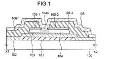
図1は、TFTの構成の一例を示す断面図であり、図2は、その上面図である。図2のX1−X2切断線に沿った断面が図1に図示されている。 FIG. 1 is a cross-sectional view showing an example of the structure of a TFT, and FIG. 2 is a top view thereof. A cross section along the X1-X2 cutting line of FIG. 2 is shown in FIG.
TFTは、基板100上に形成され、基板側から、第1の導電層101、絶縁層102、第1の半導体層103、第2の半導体層104、2つの第3の半導体層105−1、105−2が積層されている。第1の導電層101は、TFTのゲート電極を構成する導電層である。絶縁層102はTFTのゲート絶縁層を構成する。第1の半導体層はアクセプタとなる不純物元素を含む微結晶半導体でなり、TFTのチャネル形成領域を含む半導体層である。第2の半導体層104は非晶質半導体でなる。一対の第3の半導体層105−1、105−2は、それぞれ、n型またはp型の半導体でなり、ソース領域またはドレイン領域として機能する。
The TFT is formed over the
第1の半導体層103は、代表的には微結晶シリコン層であり、第2の半導体層104は、代表的には非晶質シリコン層である。また第3の半導体層105−1、105−2は、微結晶シリコン層または非晶質シリコン層である。第1の半導体層103は、結晶性に短距離秩序を持ち微結晶半導体層でなり、粒径が0.5nm以上20nm以下の微細な結晶粒が非晶質半導体中に分散して存在している半導体層である。微結晶半導体の代表例である微結晶シリコンは、そのラマンスペクトルのピークが単結晶シリコンを示す520.6cm−1よりも低波数側にシフトしている。微結晶シリコンのラマンスペクトルのピークは、代表的には481cm−1以上520.6cm−1以下の範囲に存在している。第1の半導体層103には、未結合手(ダングリングボンド)を終端するために、水素またはハロゲンを少なくとも1原子%またはそれ以上含ませることが好ましい。さらに、第1の半導体層103を構成する微結晶シリコンは格子歪みを有してもよい。ヘリウム、アルゴン、クリプトン、ネオンなどの希ガス元素を含ませて、さらに格子歪みを助長させることで、安定性が増し良好な微結晶半導体が得られる。
The
TFTには、ソース電極またドレイン電極として機能する一対の第2の導電層106−1、106−2が電気的に接続されている。第3の半導体層105−1、105−2上に、それぞれ、第2の導電層106−1、106−2が形成されている。また、TFTは、パッシベーション膜として機能する絶縁層108に覆われている。
A pair of second conductive layers 106-1 and 106-2 that function as a source electrode or a drain electrode are electrically connected to the TFT. Second conductive layers 106-1 and 106-2 are formed over the third semiconductor layers 105-1 and 105-2, respectively. The TFT is covered with an
また、第1の半導体層103は微結晶半導体で構成され、第2の半導体層104は、非晶質半導体で構成される。非晶質半導体は微結晶半導体よりもバンドギャップが大きく、抵抗が大きい。例えば、微結晶シリコンのバンドギャップは1.1eV〜1.5eV程度であり、非晶質シリコンのバンドギャップは1.6〜1.8eV程度である。また非晶質半導体は、キャリア移動度が低く、微結晶半導体の1/5〜1/10である。第1の半導体層103を微結晶半導体層で構成する微結晶半導体によりチャネル形成領域が構成される。また、第2の半導体層104は高抵抗領域として機能し、オフ状態でのリーク電流の低減、TFTの劣化抑制の効果が得られる。
In addition, the
次に、TFTの動作について説明する。ここでは、TFTが、第3の半導体層105−1、105−2がn型半導体層で構成されたnチャネル型TFTであり、第3の半導体層105−1がソース領域であり、第3の半導体層105−2がドレイン領域の場合を想定する。 Next, the operation of the TFT will be described. Here, the TFT is an n-channel TFT in which the third semiconductor layers 105-1 and 105-2 are formed of an n-type semiconductor layer, the third semiconductor layer 105-1 is a source region, The semiconductor layer 105-2 is assumed to be a drain region.
第1の導電層101に、しきい値電圧値以上の電圧を印加して、TFTをオン状態にすると、第1の半導体層103にチャネルが形成され、キャリア(この場合は電子)が第3の半導体層105−1(ソース領域)から、第2の半導体層104および第1の半導体層103を通り、第3の半導体層105−2(ドレイン領域)に移動する。すなわち、第3の半導体層105−2から第3の半導体層105−1へと電流が流れる。
When a voltage equal to or higher than the threshold voltage value is applied to the first
第1の半導体層が微結晶半導体でなるため、チャネルが非晶質半導体でなるTFTよりも、図1、図2のTFTは電界効果移動度が高く、かつオン状態で流れる電流も高くなる。これは、微結晶半導体のほうが非晶質半導体よりも、結晶性が高いため、抵抗が低くなるからである。なお、結晶性とは、固体を構成する原子配列の規則性の度合いを表現するものである。結晶性を評価する方法として、ラマン分光法、X線回折法などがある。 Since the first semiconductor layer is formed using a microcrystalline semiconductor, the TFT in FIGS. 1 and 2 has higher field effect mobility and higher current flowing in the on state than the TFT in which the channel is formed using an amorphous semiconductor. This is because a microcrystalline semiconductor has higher crystallinity than an amorphous semiconductor and thus has low resistance. In addition, crystallinity expresses the degree of regularity of the atomic arrangement which comprises solid. Examples of methods for evaluating crystallinity include Raman spectroscopy and X-ray diffraction.
なお、微結晶半導体膜は、価電子制御を目的とした不純物元素を意図的に添加しないときは、真性半導体膜ではなく、弱いn型の電気伝導性を示す半導体膜となる。その理由は、微結晶半導体膜に未結合手や欠陥があるため、自由電子が半導体に生じるからである。さらに、微結晶半導体膜を弱いn型とする原因の1つに、酸素が含まれることにある。 Note that the microcrystalline semiconductor film is not an intrinsic semiconductor film but a semiconductor film exhibiting weak n-type conductivity when an impurity element for the purpose of valence electron control is not intentionally added. The reason is that free electrons are generated in the semiconductor because the microcrystalline semiconductor film has dangling bonds and defects. Further, one of the causes of making the microcrystalline semiconductor film weak n-type is that oxygen is contained.
TFTを作製する工程では、気密性が保たれた反応室内で、CVD法またはPVD法で基板上に微結晶半導体膜成長させているが、大気成分の酸素が全く取り込まれないように基板上に微結晶半導体膜を成長させることは非常に困難であり、1×10¹⁷atoms/cm3以上の酸素が膜に混入してしまう。酸素が混入すると、微結晶半導体膜の結晶に欠陥が生じ、その欠陥により自由電子が生ずる。すなわち、微結晶半導体膜に対して、酸素はドナー不純物元素として働いている。 In the TFT manufacturing process, a microcrystalline semiconductor film is grown on the substrate by CVD or PVD in a reaction chamber that is kept airtight. It is very difficult to grow a microcrystalline semiconductor film, and oxygen of 1 × 10 17 atoms / cm 3 or more is mixed into the film. When oxygen is mixed, defects in the crystal of the microcrystalline semiconductor film are generated, and free electrons are generated due to the defects. In other words, oxygen serves as a donor impurity element for the microcrystalline semiconductor film.
よって、薄膜トランジスタのチャネル形成領域として機能する第1の半導体層103には、アクセプタとなる不純物元素を添加し、実質的に真性半導体膜となるようにすることが好ましい。アクセプタとなる不純物元素を第1の半導体層103に添加することで、TFTのしきい値電圧を制御することが可能となる。その結果、同一基板上にnチャネル型TFTおよびpチャネル型TFTを形成した場合、双方のTFTともエンハンスメント型のトランジスタとすることができる。なお、nチャネル型TFTをエンハンスメント型のトランジスタとするには、第1の半導体層103の導電型を真性または弱いp型とすればよい。
Therefore, it is preferable to add an impurity element serving as an acceptor to the
第4族元素でなる微結晶半導体膜の場合、アクセプタとなる不純物元素は代表的には、ボロンである。第1の半導体層103を真性半導体または弱いp型の導電性を示す半導体とするためには、第1の半導体層103のアクセプタ不純物元素の濃度は、1×10¹⁴〜6×10¹⁶atoms/cm3とするとよい。また酸素はドナー不純物元素として機能するだけでなく、半導体膜を酸化してTFTの電界効果移動度を低下させる原因となるため、第1の半導体層103の酸素濃度は、5×1018atoms/cm3以下が好ましく、5×1017atoms/cm3以下がより好ましい。
In the case of a microcrystalline semiconductor film formed of a Group 4 element, an impurity element that serves as an acceptor is typically boron. In order to make the
第1の導電層101の電位をしきい値電圧値よりも低くすることで、TFTはオフ状態となる。オフ状態ではTFTのソース領域とドレイン領域間に電流が流れないことが理想的である。オフ状態でソース領域とドレイン領域間を流れる電流はリーク電流と呼ばれる。図1、図2に示すような第1の半導体層103と第2の半導体層104が積層された半導体膜を有するTFTは、オフ状態では、第1の導電層101が作る電界の作用により、その半導体膜上部がリーク電流を発生するキャリアの経路となる。そこで、TFTの半導体膜において、リーク電流が流れやすい部分を、非晶質半導体でなる第2の半導体層104で構成することで、微結晶半導体でなるチャネル形成領域を有するTFTのリーク電流を低減することができる。
When the potential of the first
つまり、図1、図2に示すTFTは、チャネル形成領域が形成される半導体膜を、ゲート電極側(ゲート絶縁層側)を微結晶半導体層、ソース領域およびドレイン領域と接する側を非晶質半導体層とすることで、オン状態で流れる電流を大きくし、かつオフ状態で流れる電流を小さくすることができる。 That is, the TFT shown in FIGS. 1 and 2 includes a semiconductor film in which a channel formation region is formed, a gate electrode side (gate insulating layer side) on a microcrystalline semiconductor layer, and a side in contact with a source region and a drain region on an amorphous side. By using the semiconductor layer, the current flowing in the on state can be increased and the current flowing in the off state can be decreased.
第2の半導体層104はバッファー層として機能する。チャネル形成される第1の半導体層103の酸化を防止する役割を果たす。第1の半導体層103の酸化を防止することで、TFTの電界効果移動度が低下することを防止できる。よって、チャネル形成領域を含む第1の半導体層103を薄く形成することができる。第1の半導体層103の厚さは5nmよりも厚ければよく、その膜厚は50nm以下が好ましく、20nm以下がより好ましい。
The
また、第1の半導体層103と一対の第3の半導体層105−1、105−2(ソース領域およびドレイン領域)の間に、非晶質半導体でなる第2の半導体層104を形成することで、TFTの絶縁耐圧性を向上させことができるため、TFTの劣化が抑制され、TFTの信頼性を向上させることができる。
In addition, the
また、第1の半導体層103と一対の第3の半導体層105−1、105−2(ソース領域およびドレイン領域)の間に、非晶質半導体でなる第2の半導体層104を形成することで、寄生容量を低減することができる。
In addition, the
第2の半導体層104は、凹部104aが形成されているが、第3の半導体層105−1、105−2と重なる部分の厚さは、第1の半導体層103よりも厚く、100nm以上500nm以下とすることができる。その厚さは、200nm以上300nm以下が好ましい。ゲート電極に高い電圧(例えば15V程度)を印加してTFTを動作させるような場合でも、第2の半導体層104を100nm以上500nm以下と厚く形成することで、TFTが劣化することを抑制することができる。
The
また、非晶質半導体でなる第2の半導体層104を形成することで、TFTの電気的特性を向上させ、かつ信頼性を向上させることが、半導体膜の酸化による薄膜トランジスタの電気特性の低下、薄膜トランジスタの寄生容量の増大、および、高電圧を印加した際の薄膜トランジスタの劣化を抑制しつつ、チャネル形成領域となる第1の半導体層103の薄膜化が可能となる。
In addition, by forming the
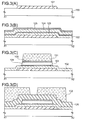
次に、図3および図4を参照して、図1、図2の薄膜トランジスタの作製方法を説明する。 Next, a method for manufacturing the thin film transistor of FIGS. 1 and 2 will be described with reference to FIGS.
まず、基板100を用意する。基板100は、バリウムホウケイ酸ガラス、アルミノホウケイ酸ガラス、若しくはアルミノシリケートガラスなど、フュージョン法やフロート法で作製される無アルカリガラス基板、セラミック基板の他、本作製工程の処理温度に耐えうる耐熱性を有するプラスチック基板などを用いることができる。また、ステンレス合金などの金属基板の表面に絶縁膜を設けた基板を適用してもよい。
First, the
次に、基板100上に第1の導電層101を形成する(図3(A)参照)。まず、チタン、モリブデン、クロム、タンタル、タングステン、アルミニウムなどの金属またはこれらの金属を含む合金から選択される導電性材料でなる単層構造または積層構造の導電膜を形成する。この導電膜の形成には、スパッタ法や真空蒸着法を用いることができる。そして、当該導電膜上にフォトリソグラフィ技術またはインクジェット法によりマスクを形成し、当該マスクを用いて導電膜をエッチングすることで、所定の形状を有する第1の導電層101が形成される。
Next, the first
また、エッチング処理を行わないで第1の導電層101を形成することが可能である。銀、金、銅などの導電性ナノペーストをインクジェット法により、所定の形状になるように吐出し、しかる後焼成して、所定の形状を有する第1の導電層101を形成することもできる。なお、第1の導電層101の密着性向上、および金属元素の拡散を防ぐバリア層として、金属の窒化物膜を、基板100および第1の導電層101の間に設けることもできる。バリア層は、チタン、モリブデン、クロム、タンタル、タングステン、またはアルミニウムの窒化物膜で形成することができる。
In addition, the first
第1の導電層101上には半導体膜や配線を形成するので、これらの段切れ防止のため、第1の導電層101の端部がテーパー状になるように加工することが望ましい。図3では、第1の導電層101の端部をテーパー状に加工している。
Since a semiconductor film or a wiring is formed over the first
次に、絶縁層102、第1の半導体層103を構成する微結晶半導体層123、非晶質半導体層124、および、n型またはp型の半導体層125の順に、各層を第1の導電層101上に形成する(図3(B)参照)。微結晶半導体層123の厚さは5nmよりも厚ければよく、その膜厚は、50nm以下、好ましくは20nm以下である。非晶質半導体層124は、100nm以上500nm以下、好ましくは200nm以上300nm以下の厚さで形成する。
Next, the insulating
絶縁層102、微結晶半導体層123、非晶質半導体層124、n型またはp型の半導体層125は、連続的に形成することが好ましい。すなわち、絶縁層102を形成した後、基板100を大気に触れさせることなく、半導体層123〜125を連続成膜する。このように形成することで、酸素、窒素などの大気成分元素、大気中に浮遊する汚染不純物元素で各層の界面で汚染されることを防止できるため、電気特性のTFTごとのばらつきを低減することができる。
The insulating
絶縁層102は酸化シリコン膜、窒化シリコン膜、酸化窒化シリコン膜、または窒化酸化シリコン膜で形成することができる。これらの絶縁膜は、それぞれ、CVD法やスパッタ法で形成することができる。CVD法でこれらの絶縁膜を形成する場合、PECVD法が好ましく、特に周波数が1GHz以上のマイクロ波でプロセスガスを励起してプラズマを生成することが好ましい。マイクロ波励起のプラズマを用いて気相成長させた酸化窒化シリコン膜、窒化酸化シリコン膜は、絶縁耐圧が高いため、TFTの信頼性を向上させることができる。
The insulating
なお、酸化窒化シリコンとは、その組成として、窒素よりも酸素の含有量が多いものであって、濃度範囲として酸素が55〜65原子%、窒素が1〜20原子%、Siが25〜35原子%、水素が0.1〜10原子%の範囲で含まれるものをいう。また、窒化酸化シリコンとは、その組成として、酸素よりも窒素の含有量が多いものであって、濃度範囲として酸素が15〜30原子%、窒素が20〜35原子%、Siが25〜35原子%、水素が15〜25原子%の範囲で含まれるものをいう。 Note that silicon oxynitride has a higher oxygen content than nitrogen in its composition, and the concentration ranges of oxygen are 55 to 65 atomic%, nitrogen is 1 to 20 atomic%, and Si is 25 to 35. An atomic% and what contains hydrogen in the range of 0.1-10 atomic%. In addition, silicon nitride oxide has a composition containing more nitrogen than oxygen, and the concentration ranges of oxygen are 15 to 30 atomic%, nitrogen is 20 to 35 atomic%, and Si is 25 to 35. An atomic% and a thing containing hydrogen in the range of 15-25 atomic%.
絶縁層102は単層構造、積層構造とすることができる。例えば、絶縁層102を2層構造とする場合は、下層を酸化シリコン膜または酸化窒化シリコン膜で形成し、上層を窒化シリコン膜または窒化酸化シリコン膜で形成する。3層構造とする場合は、基板100側の層を窒化シリコン膜または窒化酸化シリコン膜で形成し、中央の層を酸化シリコン膜または酸化窒化シリコン膜で形成し、微結晶半導体層123側の層を窒化シリコン膜または窒化酸化シリコン膜で形成することができる。
The insulating
微結晶半導体層123は、結晶性に短距離秩序を持ち、粒径が0.5nm以上20nm以下の微細な結晶粒が非晶質半導体中に存在している半導体層である。
The
微結晶半導体層は、PECVD法で形成される。プロセスガスには、シリコンソースガスの他、水素を混合することができる。また、プロセスガスにヘリウム、アルゴン、クリプトン、ネオンなどの希ガスを混合することができる。プロセスガス中のヘリウム、アルゴン、クリプトン、ネオンなどの希ガスの濃度を調節することで、微結晶半導体層123にこれらの希ガス元素を添加することができる。
The microcrystalline semiconductor layer is formed by a PECVD method. In addition to the silicon source gas, hydrogen can be mixed in the process gas. Further, a rare gas such as helium, argon, krypton, or neon can be mixed with the process gas. These rare gas elements can be added to the
また、ハロゲン元素を組成とする物質の気体(F2、Cl2、Br2、I2、HF、HCl、HBr、HIなど)をプロセスガスに混合すること、または、組成にハロゲンを含むシリコンソースガス(SiH2Cl2、SiHCl3、SiCl4、SiF4など)を用いることで、微結晶半導体層123にハロゲンを添加することができる。例えば、SiF4を用いる場合は、シリコンソースガスとしては、SiF4とSiH4の混合ガスを用いることが望ましい。
In addition, a gas containing a substance containing a halogen element (F 2 , Cl 2 , Br 2 , I 2 , HF, HCl, HBr, HI, or the like) is mixed with a process gas, or a silicon source containing a halogen in the composition By using gas (SiH 2 Cl 2 , SiHCl 3 , SiCl 4 , SiF 4, or the like), halogen can be added to the
また、微結晶半導体層123には、アクセプタ不純物元素を添加し、真性半導体層、または弱いn型の半導体層とする。微結晶半導体層123のアクセプタ不純物元素の濃度は、例えば1×10¹⁴〜6×10¹⁶atoms/cm3とするとよい。微結晶半導体層123をCVD法で形成する場合は、プロセスガスにアクセプタ不純物元素を含むドーパントガスを混合する。微結晶半導体層123中のアクセプタ不純物元素の濃度は、ドーパントガスの分圧で調節することができる。ドーパントガスの分圧は、反応室に供給する際のドーパントガスの流量およびその希釈率で調節することができる。例えば、雰囲気の圧力が150Pa±20Pa程度の場合、ドーパントガスの分圧は1×10−8Pa以上1×10−5Pa以下とするとよい。
In addition, an acceptor impurity element is added to the
アクセプタ不純物元素は、代表的にはボロンである。アクセプタ不純物元素を含むドーパントガスには、B2H6、BF3、BCl3、BBr3、トリメチルボロン(B(CH3)3)などから選ばれるガスを用いることができる。B2H6は吸着しやすく、プラズマクリーニングで反応室からの除去が困難である。トリメチルボロン(以下、「TMB」と記す)は、プラズマクリーニングでB2H6よりも反応室から除去しやすいという利点がある。また、TMBはB2H6よりも分解しにくいため、保存期間が長いという長所もある。 The acceptor impurity element is typically boron. As the dopant gas containing an acceptor impurity element, a gas selected from B 2 H 6 , BF 3, BCl 3 , BBr 3 , trimethyl boron (B (CH 3 ) 3 ), and the like can be used. B 2 H 6 is easily adsorbed and difficult to remove from the reaction chamber by plasma cleaning. Trimethylboron (hereinafter referred to as “TMB”) has an advantage that it is easier to remove from the reaction chamber than B 2 H 6 by plasma cleaning. In addition, since TMB is harder to decompose than B 2 H 6 , there is an advantage that the storage period is long.
微結晶半導体層123として微結晶シリコン膜を形成する場合、プロセスガスには、少なくとも、シリコンソースガス、ドーパントガスおよび水素が含まれる。水素の代わりにヘリウムなどの希ガスを混合することができる。微結晶シリコン膜を形成するには、シリコンソースガスの分圧に対する水素の分圧比(水素/シリコンソースガス)が50以上であることが好ましく、その分圧比50以上2000以下とすることができる。分圧比を大きくすることで、シリコン膜の成長速度が下がるため、結晶核を発生しやすくなり、膜が微結晶化する。基板の加熱温度は100℃以上300℃以下とすることができる。また、雰囲気の圧力を100Pa以上300Pa以下とすることができる。
In the case of forming a microcrystalline silicon film as the
また、微結晶半導体層123の酸素濃度は1×10¹⁹atoms/cm3以下が好ましく、5×1018atoms/cm3以下がより好ましい。酸素を減らすには、基板100に吸着する酸素を減らす、また微結晶半導体層123を形成する反応室内にリークする空気の量を減らす、および、微結晶半導体層123の成膜速度を上げることにより、成膜時間を短くするなどの方法がある。
The oxygen concentration of the
微結晶半導体層123を形成するために、周波数の異なる高周波電力をプロセスガスに供給し、プロセスガスを励起させる。PECVD装置の電極に周波数の異なる2以上の高周波電力を供給することで、周波数の異なる高周波電力をプロセスガスに供給することができる。このことにより、プロセスガスを励起してプラズマを生成して、微結晶半導体層123を形成する。なお、周波数が異なると、波長が異なる。
In order to form the
電極に印加される高周波電力は少なくとも2種類ある。1つは表面定在波効果が現れない周波数帯の電力である。その波長は概ね10m以上である。もう1つは、もう一方の高周波電力よりも波長が短い高周波電力である。PECVD装置の電極に、このような2種類の高周波電力を重畳して印加することで、プラズマの高密度化を図ることができる。また、プラズマ表面定在波効果が抑制されるため、プラズマの均一化を図ることができる。 There are at least two types of high-frequency power applied to the electrodes. One is power in a frequency band where the surface standing wave effect does not appear. The wavelength is approximately 10 m or more. The other is high-frequency power having a shorter wavelength than the other high-frequency power. By superimposing and applying such two types of high-frequency power to the electrodes of the PECVD apparatus, the plasma density can be increased. Moreover, since the plasma surface standing wave effect is suppressed, the plasma can be made uniform.
図19は複数の高周波電力が印加されるPECVD装置の一構成例を示す。反応室500はアルミニウム又はステンレスなど剛性のある素材で形成され、内部を真空排気できるように構成されている。反応室500には第1の電極501と第2の電極502が備えられている。
FIG. 19 shows a configuration example of a PECVD apparatus to which a plurality of high frequency powers are applied. The
第1の電極501には高周波電力供給手段503が連結され、第2の電極502は接地電位が与えられ、基板を載置できるように構成されている。第1の電極501は絶縁材516により反応室500と絶縁分離され、高周波電力が漏洩しないように構成されている。なお、図19では、第1の電極501と第2の電極502の構成は、容量結合型(平行平板型)の構成例を示しているが、異なる2以上の高周波電力を印加して反応室500の内部にプラズマを生成できるものであれば、誘導結合型など他の構成を適用することもできる。
High-frequency power supply means 503 is connected to the
高周波電力供給手段503には、第1の高周波電源504と第2の高周波電源505、およびそれらに対応して第1の整合器506と第2の整合器507が含まれる。第1の高周波電源504と第2の高周波電源505から出力される高周波電力は、共に第1の電極501に供給される。第1の整合器506又は第2の整合器507の出力側には、一方の高周波電力が流入しないように帯域通過フィルタを設けてもよい。
The high-frequency power supply means 503 includes a first high-
第1の電極501はガス供給手段508にも連結されている。ガス供給手段508は、SiH4など各種のガスが充填されるシリンダ510、圧力調整弁511、ストップバルブ512、マスフローコントローラ513などで構成されている。TMBや、PH3などのドーパントガスは、H2やHeなどのガスで希釈された状態でシリンダ510に充填されている。
The
反応室500内において、第1の電極501は基板と対向する面がシャワー板状に加工され、その面に多数の細孔が設けられている。第1の電極501に供給される反応ガスは、内部の中空構造を通り、この細孔から反応室500内に供給される。
In the
第2の電極502には、基板加熱ヒータ514と、基板加熱ヒータ514の温度制御を行うヒータコントローラ515が設けられている。基板加熱ヒータ514は第2の電極502内に設けられる場合、熱伝導加熱方式が採用され、シースヒータなどで構成される。第1の電極501と第2の電極502の間隔は適宜変更できるように、第2の電極502の高さ調節ができるように可動式となる構成が含まれる。
The
反応室500に接続される排気手段509は、真空排気の場合や、反応ガスを流す場合において、反応室500内を所定の圧力に保持するように制御する機能が含まれている。
The exhaust means 509 connected to the
排気手段509の構成としては、バタフライバルブ517、コンダクタンスバルブ518、ターボ分子ポンプ519、ドライポンプ520などが含まれる。バタフライバルブ517とコンダクタンスバルブ518を並列に配置する場合には、バタフライバルブ517を閉じてコンダクタンスバルブ518を動作させることで、反応ガスの排気速度を制御して反応室500の圧力を所定の範囲に保つことができる。また、コンダクタンスの大きいバタフライバルブ517を開くことで高真空排気が可能となる。
The configuration of the exhaust means 509 includes a
真空度として10−5Paよりも低い圧力の超高真空排気する場合には、クライオポンプ521を併用することが好ましい。微結晶半導体層123の酸素濃度を1×10¹⁷atoms/cm3以下とするには、微結晶半導体層123を形成する前に、反応室500を超高真空まで排気することは有効である。なお、反応室500の到達真空度を超高真空とするには、反応室500の内壁を鏡面加工し、内壁からのガス放出を低減するためにベーキング用のヒータを設けることが効果的である。
When performing ultra-high vacuum evacuation at a pressure lower than 10 −5 Pa as the degree of vacuum, it is preferable to use a
第1の高周波電源504が供給する高周波電力は、概ね波長として10m以上の高周波が適用される。HF帯である3MHzから30MHz、代表的には13.56MHzの周波数の高周波電力が第1の高周波電源504から供給される。
The high frequency power supplied from the first high
第2の高周波電源505が供給する高周波電力は、その周波数がVHF帯にあり、概ね波長が10m未満である。具体的には、第2の高周波電源505からは30MHz〜300MHzの高周波電力が供給される。
The high-frequency power supplied from the second high-
すなわち、第1の高周波電源504が供給する高周波の波長は、第1の電極501の1辺の長さの3倍以上を有する。第2の高周波電源505が供給する高周波の波長は、第1の高周波電源504が供給する高周波の波長よりも短い波長を適用する。表面定在波を引き起こさない高周波電力を第1の電極501に供給してプラズマを生成するとともに、VHF帯に属する高周波電力を供給してプラズマの高密度化をすることで、結晶性の高い微結晶半導体層123を形成することが可能になる。また、長辺が2000mmを超える大面積基板に膜質の良い薄膜を均一な厚さで形成することが可能となる。
In other words, the wavelength of the high frequency supplied by the first high
プロセスガスの励起は、周波数の異なる第1の高周波電力および第2の高周波電力を第1の電極501に重畳して印加することで行われる。第1の高周波電力の周波数は3MHzから30MHz、代表的には13.56MHである。第2の高周波電力の周波数は、30MHzより大きく300MHz程度までのVHF帯である。表面定在波の影響が出ない周波数帯の第1の高周波電力によってプロセスガス励起して、プラズマを生成するとともに、VHF帯に属する第2の高周波電力もプロセスガスに供給することで、プラズマの高密度化ができる。さらに、表面定在波の影響が抑えられるため、長辺が2000mmを超える大面積基板上にも、均一な厚さで膜質の良い薄膜を形成することが可能となる。
The process gas is excited by superimposing and applying the first high-frequency power and the second high-frequency power having different frequencies to the
プロセスガスにヘリウムを混合することができる。ヘリウムは24.5eVとすべての気体中で最も高いイオン化エネルギーを持ち、そのイオン化エネルギーよりも少し低い、約20eVの準位に準安定状態があるので、放電持続期間では、イオン化にはその差約4eVしか必要としない。そのため、ヘリウムは、放電開始電圧も全ての気体中最も低い値を示す。このような特性から、ヘリウムをプロセスガスに混合することで、プラズマを安定的に維持することができる。このことから、均一なプラズマを形成することができるので、微結晶シリコン膜を堆積する基板の面積が大きくなってもプラズマ密度の均一化の効果を奏する。 Helium can be mixed into the process gas. Helium has the highest ionization energy of all gases at 24.5 eV, and there is a metastable state at a level of about 20 eV, which is slightly lower than the ionization energy. Only 4 eV is required. Therefore, helium also has the lowest discharge start voltage among all gases. From such characteristics, the plasma can be stably maintained by mixing helium with the process gas. Thus, uniform plasma can be formed, and the plasma density can be made uniform even when the area of the substrate on which the microcrystalline silicon film is deposited is increased.
微結晶半導体層123を形成する前に、その被形成面となる絶縁層102の表面をプラズマ処理することが好ましい。このプラズマ処理は、希ガスプラズマ処理、水素プラズマ処理、若しくは両処理の併用が好ましい。
Before the
希ガスプラズマ処理には、アルゴン、クリプトン、キセノンなど質量数の大きい希ガス元素を用いることが好ましい。絶縁層102表面に付着した酸素、水分、有機物、金属元素などをスパッタリングの効果で除去するためである。水素プラズマ処理は、水素ラジカルによる、絶縁層102表面に吸着した前記不純物の除去と、絶縁層102に対するエッチング作用により、微結晶半導体層123の被形成面を清浄にするのに有効である。また、希ガスプラズマ処理と水素プラズマ処理を併用することにより、微結晶核生成を促進する作用も期待される。また、微結晶核の生成を促進させる目的のため、微結晶シリコン膜の成膜初期段階において、反応室500に、シリコンソースガスと共に、継続的にアルゴンなどの希ガスを供給することは有効である。
In the rare gas plasma treatment, a rare gas element having a large mass number such as argon, krypton, or xenon is preferably used. This is because oxygen, moisture, organic substances, metal elements, and the like attached to the surface of the insulating
非晶質半導体層124は、PECVD法などのCVD法、スパッタ法などのPVD法で形成することができる。CVD法で非晶質シリコン膜を形成する場合、シリコンソースガスには、SiH4、Si2H6、SiH2Cl2、SiHCl3、SiCl4、SiF4などから選ばれる1種類または複数種類のガスを用いることができる。例えば、SiF4を用いる場合は、シリコンソースガスとしては、SiF4とSiH4の混合ガスを用いることが望ましい。また、CVD法のプロセスガスには、シリコンソースガスの他、水素に加え、ヘリウム、アルゴン、クリプトン、ネオンを混合することができる。また、ハロゲン元素を組成とする物質の気体(F2、Cl2、Br2、I2、HF、HCl、HBr、HIなど)をプロセスガスに混合すること、または、組成にハロゲンを含むシリコンソースガス(SiH2Cl2、SiHCl3、SiCl4、SiF4など)を用いることで、非晶質シリコン膜にハロゲンを添加することができる。
The
また、スパッタ法で非晶質シリコン膜を形成は、ターゲットに単結晶シリコンを用い、希ガスでターゲットをスパッタリングすることで行うことができる。また、膜の形成時に、アンモニア、窒素、またはN2Oを雰囲気中に含ませることにより、窒素を含む非晶質シリコン膜を形成することができる。また、雰囲気中にハロゲンを組成とする気体(F2、Cl2、Br2、I2、HF、HCl、HBr、HIなど)を含ませることにより、フッ素、塩素、臭素、またはヨウ素を含む非晶質半導体膜を形成することができる。 The amorphous silicon film can be formed by sputtering using single crystal silicon as a target and sputtering the target with a rare gas. In addition, an amorphous silicon film containing nitrogen can be formed by including ammonia, nitrogen, or N 2 O in the atmosphere when forming the film. In addition, by containing a gas having a halogen composition (F 2 , Cl 2 , Br 2 , I 2 , HF, HCl, HBr, HI, or the like) in the atmosphere, non-containing gas including fluorine, chlorine, bromine, or iodine. A crystalline semiconductor film can be formed.
また、非晶質半導体層124を形成した後、非晶質半導体層124の表面を水素プラズマ、窒素プラズマ、またはハロゲンプラズマで処理して、非晶質半導体層124の表面を水素化、窒素化、またはハロゲン化してもよい。または、非晶質半導体層124の表面を、ヘリウムプラズマ、ネオンプラズマ、アルゴンプラズマ、クリプトンプラズマなどの希ガスプラズマ処理してもよい。
In addition, after the
一導電型を付与する不純物が添加された半導体層125は、ソース領域およびドレイン領域を構成する半導体層であり、微結晶半導体または非晶質半導体でなる。半導体層125は微結晶半導体層123、非晶質半導体層124と同様に形成することができ、半導体層125を形成するときにドナー不純物元素またはアクセプタ不純物元素を含ませる。半導体層125は2nm以上50nm以下の厚さで形成される。
The
nチャネル型TFTを形成するためには、ドーパント不純物元素としてリンを添加して、n型の導電性を半導体層125に付与する。そのため、CVD法で半導体層125を形成するには、PH3などのドナー元素を組成に含むドーパントガスをプロセスガスに混合する。他方、pチャネル型TFTを形成するためには、アクセプタ不純物元素としてボロンを添加して、p型の導電性を半導体層125に付与する。そのため、CVD法で半導体層125を形成するには、B2H6、BF3、BCl3、BBr3、TMBなどのアクセプタ元素を組成に含むドーパントガスをプロセスガスに混合する。半導体層125は2nm以上50nm以下の厚さで形成する。一導電型を付与する不純物が添加された半導体膜の膜厚を薄くすることで、スループットを向上させることができる。
In order to form an n-channel TFT, phosphorus is added as a dopant impurity element to impart n-type conductivity to the
次に、半導体層125上に、マスク131を形成する。マスク131は、フォトリソグラフィ技術又はインクジェット法により形成する。マスク131を用いて、半導体層125、非晶質半導体層124および微結晶半導体層123をエッチングして、第3の半導体層105、第2の半導体層104、および第1の半導体層103を形成する(図3(C)参照)。つまり、エッチング工程により、絶縁層102上に、第3の半導体層105、第2の半導体層104、および第1の半導体層103でなる島状の3層構造の積層体が形成される。
Next, a
図3(C)の工程では、第3の半導体層105は、ソース領域とドレイン領域に分割されていない。第2の半導体層104、および第1の半導体層103の全体は、第1の導電層101と重なるように形成される。この構造により、基板100を透過した光が第1の導電層101によって遮られるため、光が第2の半導体層104、第1の半導体層103に照射されることが防止され、光リーク電流の発生を回避できる。
In the step of FIG. 3C, the
次に、エッチングにより残存した第3の半導体層105および絶縁層102上に導電層126を形成し、当該導電層126上にマスク132を形成する(図3(D)参照)。マスク132は、フォトリソグラフィ技術又はインクジェット法により形成する。
Next, a
導電層126は、単層構造、積層構造とすることができる。ソース電極、ドレイン電極の低抵抗化のため、少なくとも1層は、アルミニウム、アルミニウム合金、または銅でなる導電膜を設けることが好ましい。アルミニウムには、チタン、ネオジム、スカンジウム、モリブデンなどを微量添加して、耐熱性を向上させることが好ましい。またアルミニウム合金には、これらの元素とアルミニウムとの合金を用いて、耐熱性を向上させることが好ましい。導電層126を構成する導電膜は、スパッタ法や真空蒸着法で形成することができる。
The
導電層126を2層構造とする場合は、下層を耐熱性金属膜、または耐熱性金属の窒化物膜で形成し、上層をアルミニウム、アルミニウム合金、または銅でなる膜で形成する。なお、耐熱性金属とはアルミニウムよりも融点が高い(800℃以上が好ましい)金属であり、例えば、チタン、タンタル、モリブデン、タングステンなどである。導電層126を3層構造とする場合は、中央の層をアルミニウム、アルミニウム合金、または銅でなる膜で形成し、上層および下層を耐熱性金属膜、または耐熱性金属の窒化物膜で形成する。すなわち、3層構造の場合、アルミニウム膜などの低抵抗な導電膜を、耐熱性の高い導電膜で挟んだ構造とすることが好ましい。導電層126を構成する導電膜は、スパッタ法や真空蒸着法で形成することができる。
In the case where the
なお、図3(B)の工程で、さらに半導体層125上に導電層126を形成することもできる。
Note that the
次に、マスク132を用いて導電層126をエッチングして、一対の第2の導電層106−1、106−2を形成する(図4(A)参照)。
Next, the
さらに、マスク132を用いて第3の半導体層105をエッチングして一対の第3の半導体層105−1、105−2を形成する(図4(B)参照)。第3の半導体層105のエッチング剤により、第2の半導体層104もエッチングされ、凹部104aが形成される。凹部104aが形成される領域は、第3の半導体層105−1、105−2および、一対の第2の導電層106−1、106−2と重なっていない領域である。この領域は、図2の上面図において、第2の半導体層104が露出している領域である。第3の半導体層105−1、105−2の端部と第2の導電層106−1、106−2の端部はほぼ一致している。
Further, the
第2の半導体層104を、第1の半導体層103の酸化防止のバッファー層として機能させるためには、このエッチング処理で、第1の半導体層103が露出しないように、第2の半導体層104をエッチングする必要がある。
In order for the
次に、第2の導電層106−1、106−2の周辺部をエッチングする(図4(C))。ここでは、マスク132を用いて、ウエットエッチングするため、第2の導電層106−1、106−2の側面の露出部がエッチングされる。したがって、第2の導電層106−1と第2の導電層106−2間の距離をTFTのチャネル長よりも長くできる。このことにより、第2の導電層106−1と第2の導電層106−2間の距離を長くすることができるので、第2の導電層106−1と第2の導電層106−2とのショートを防止することができる。
Next, the periphery of the second conductive layers 106-1 and 106-2 is etched (FIG. 4C). Here, in order to perform wet etching using the
図4(C)のエッチング処理を行うことで、第2の導電層106−1、106−2の端部は、第3の半導体層105−1、105−2の端部からずれる。すなわち、図2に示すように、第2の導電層106−1、106−2の外側に第3の半導体層105−1、105−2の端部が存在する。このような構造にすることで、TFTのソース電極およびドレイン電極、ソース領域およびドレイン領域の端部に電界が集中せず、ゲート電極と、ソース電極およびドレイン電極との間でのリーク電流を防止することができる。このため、信頼性が高く、且つ耐圧の高い薄膜トランジスタを作製することができる。 By performing the etching treatment in FIG. 4C, the end portions of the second conductive layers 106-1 and 106-2 are shifted from the end portions of the third semiconductor layers 105-1 and 105-2. That is, as shown in FIG. 2, the end portions of the third semiconductor layers 105-1 and 105-2 exist outside the second conductive layers 106-1 and 106-2. With this structure, the electric field is not concentrated on the edge of the source and drain electrodes, the source region and the drain region of the TFT, and leakage current between the gate electrode and the source and drain electrodes is prevented. can do. Therefore, a thin film transistor with high reliability and high withstand voltage can be manufactured.
しかる後、マスク132を除去する。なお、図4(C)のエッチング処理を行わないで、第3の半導体層105−1、105−2の端部と第2の導電層106−1、106−2の端部はほぼ一致している構成とすることもできる。次に、絶縁層108を形成する(図1参照)。絶縁層108は、絶縁層102と同様に形成することができる。なお、絶縁層108は、大気中に浮遊する有機物や金属物、水蒸気などの汚染不純物の侵入を防ぐためのものであり、窒化シリコン膜など緻密な膜が好ましい。以上により、図1、図2に示すチャネルエッチ構造のTFTが完成する。
Thereafter, the
本実施形態では、微結晶半導体層123の形成工程で、図19のPECVD装置を用いて形成する方法を説明したが、図19のPECVD装置で、微結晶半導体層123の他の、絶縁層102、非晶質半導体層124、半導体層125および絶縁層108を形成することができる。
In this embodiment mode, the method for forming the
図19のPECVD装置では、反応ガスを替えれば各種薄膜を形成することができる。半導体層としては、非晶質シリコン膜、非晶質シリコンゲルマニウム膜、非晶質シリコンカーバイト膜、微結晶シリコンゲルマニウム膜、微結晶シリコンカーバイト膜などの成膜に本形態を置き換えることができる。絶縁層としては、酸化シリコン膜、窒化シリコン膜、酸化窒化シリコン膜、窒化酸化シリコン膜などを成膜することができる。すなわち、これら半導体層、絶縁層を形成するために、周波数の異なる2種類の高周波電力をプロセスガスに供給し、プロセスガスを励起させるPECVD法を用いることができる。したがって、本実施形態では、微結晶半導体層123と同様なPECVD法で、絶縁層102、非晶質半導体層124、半導体層125および絶縁層108を形成することができる。
In the PECVD apparatus of FIG. 19, various thin films can be formed by changing the reaction gas. As the semiconductor layer, the present embodiment can be replaced with an amorphous silicon film, an amorphous silicon germanium film, an amorphous silicon carbide film, a microcrystalline silicon germanium film, a microcrystalline silicon carbide film, or the like. . As the insulating layer, a silicon oxide film, a silicon nitride film, a silicon oxynitride film, a silicon nitride oxide film, or the like can be formed. That is, in order to form these semiconductor layers and insulating layers, a PECVD method can be used in which two types of high frequency power having different frequencies are supplied to the process gas to excite the process gas. Therefore, in this embodiment, the insulating
(実施形態2)
本実施形態では、実施形態1と異なる構造の薄膜トランジスタおよびその作製方法を説明する。実施形態1では、チャネルエッチ型の薄膜トランジスタを示したが、本実施形態では、チャネル形成領域上に絶縁膜でなる保護層を有する薄膜トランジスタについて説明する。このような保護層を有するTFTの構造を「チャネル保護型」と呼ぶ。図5は、チャネル保護型TFTの構成の一例を示す断面図であり、図6はその上面図である。図6のY1−Y2切断線に沿った断面図が図5である。
(Embodiment 2)
In this embodiment mode, a thin film transistor having a structure different from that in Embodiment Mode 1 and a manufacturing method thereof will be described. In Embodiment 1, a channel-etched thin film transistor is shown; however, in this embodiment, a thin film transistor having a protective layer made of an insulating film over a channel formation region will be described. The structure of a TFT having such a protective layer is called a “channel protection type”. FIG. 5 is a cross-sectional view showing an example of the configuration of the channel protection type TFT, and FIG. 6 is a top view thereof. FIG. 5 is a cross-sectional view taken along the line Y1-Y2 in FIG.
本実施形態のTFTが実施形態1と異なる点は次の通りである。第2の半導体層104に凹部104aが形成されていなく、第2の半導体層104上に保護層109が形成されている。また、図6に示すように、第2の半導体層104は露出していなく、第3の半導体層105−1、105−2、保護層109によって覆われている。また、第2の導電層106−1、106−2の全体は第3の105−1、105−2と重なっている。また、第2の導電層106−1、106−2の端部は、第3の半導体層105−1、105−2の端部からずれている点、および、第1の半導体層103および第2の半導体層104の全体が第1の導電層101と重なっている点は、実施形態1のTFTと同様である。
The TFT of this embodiment is different from that of Embodiment 1 as follows. The recessed
次に、図7および図8を参照して、図5および図6のTFTの作製方法を説明する。本実施形態のTFTの作製工程は、実施形態1の作製方法を適用できる。 Next, a method for manufacturing the TFT of FIGS. 5 and 6 will be described with reference to FIGS. The manufacturing method of Embodiment 1 can be applied to the manufacturing process of the TFT of this embodiment.
まず、基板100上に第1の導電層101を形成した後、絶縁層102、微結晶半導体層123、非晶質半導体層124を積層する。さらに非晶質半導体層124上に保護層109を形成する(図7(A)参照)。保護層109は絶縁層102と同様に形成した絶縁層、または非感光性の有機材料層をエッチングにより島状に加工することで、形成することができる。
First, after the first
次に、保護層109および非晶質半導体層124上に図3(C)と同様なマスク(図示せず)を形成し、このマスクを用いて、図3(C)と同様にエッチング処理を行い、第1の半導体層103、第2の半導体層104を形成する(図7(B)参照)。この後、マスクを除去する。
Next, a mask (not shown) similar to that in FIG. 3C is formed over the
次に、絶縁層102、第2の半導体層104、保護層109上に、半導体層125および導電層126を順に積層して形成する(図7(C)参照)。
Next, the
次に、導電層126上にマスク133を形成する。マスク133を用いて、図4(A)と同様に導電層126をエッチングして、一対の第2の導電層106−1、106−2を形成する(図8(A)参照)。
Next, a
さらに、マスク133を用いて、図4(B)と同様に、半導体層125をエッチングして一対の第3の半導体層105−1、105−2を形成する(図8(B)参照)。このエッチング工程では、保護層109がエッチングストッパとして機能するため、第2の半導体層104に凹部が形成されない。導電層126および半導体層125を積層して形成したこと、共通のマスク133を用いて導電層126および半導体層125をエッチングしているため、導第3の半導体層105−1、105−2が存在している領域に、第2の導電層106−1、106−2が存在する。また、第3の半導体層105−1、105−2の端部と第2の導電層106−1、106−2の端部はほぼ一致している。
Further, using the
次に、図4(C)と同様に、第2の導電層106−1、106−2の周辺部をエッチングする(図8(C))。この工程で、第2の導電層106−1、106−2の端部は、第3の半導体層105−1、105−2の端部からずれる。すなわち、図6に示すように、第2の導電層106−1、106−2の外側に第3の半導体層105−1、105−2の端部が存在する。このような構造にすることで、TFTのソース電極およびドレイン電極、ソース領域およびドレイン領域の端部に電界が集中せず、ゲート電極と、ソース電極およびドレイン電極との間でのリーク電流を防止することができる。このため、信頼性が高く、且つ高絶縁耐圧の薄膜トランジスタを作製することができる。 Next, as in FIG. 4C, the peripheral portions of the second conductive layers 106-1 and 106-2 are etched (FIG. 8C). In this step, the end portions of the second conductive layers 106-1 and 106-2 are shifted from the end portions of the third semiconductor layers 105-1 and 105-2. That is, as shown in FIG. 6, the end portions of the third semiconductor layers 105-1 and 105-2 exist outside the second conductive layers 106-1 and 106-2. With this structure, the electric field is not concentrated on the edge of the source and drain electrodes, the source region and the drain region of the TFT, and leakage current between the gate electrode and the source and drain electrodes is prevented. can do. Therefore, a thin film transistor with high reliability and high withstand voltage can be manufactured.
しかる後、マスク133を除去する。なお、図8(C)のエッチング処理を行わないことで、第3の半導体層105−1、105−2の端部と第2の導電層106−1、106−2の端部がほぼ一致している構成とすることもできる。次に、絶縁層108を形成する(図5参照)。以上により、図5、図6に示すチャネル保護型のTFTが完成する。
Thereafter, the
(実施形態3)
本実施形態では、トランジスタを有する半導体装置の一例として、アクティブマトリクス型表示装置について説明する。アクティブマトリクス型表示装置は、画素部の各画素にトランジスタを有する。
(Embodiment 3)
In this embodiment, an active matrix display device will be described as an example of a semiconductor device having a transistor. An active matrix display device includes a transistor in each pixel of a pixel portion.
まず、図面を用いて、本発明のアクティブマトリクス型表示装置の構成について説明する。図9は、アクティブマトリクス型表示装置の構成例を示すブロック図である。アクティブマトリクス型表示装置は、画素部10、ソース線駆動回路11、走査線駆動回路12、ソース線駆動回路11に接続された複数のソース線13、および走査線駆動回路12に接続された複数の走査線14を有する。
First, the configuration of the active matrix display device of the present invention will be described with reference to the drawings. FIG. 9 is a block diagram illustrating a configuration example of an active matrix display device. The active matrix display device includes a
複数のソース線13は列方向に配列され、複数の走査線14はソース線13と交差して行方向に配列されている。画素部10には、ソース線13および走査線14がつくる行列に対応して、複数の画素15が行列状に配列されている。画素15は、走査線14およびソース線13に接続されている。画素15はスイッチング素子および表示素子を含む。スイッチング素子は、走査線14に入力される信号に従って、画素が選択か非選択かを制御する。表示素子はソース線13から入力されるビデオ信号によって階調が制御される。
The plurality of
図10および図11を用いて、画素15の構成例を説明する。本発明をアクティブマトリクス型液晶表示装置に適用した場合の、画素15の構成例を図10に示す。図10は画素の回路図である。画素15は、スイッチング素子としてスイッチングトランジスタ21を有し、表示素子として液晶素子22を有する。スイッチングトランジスタ21はゲートが走査線14に接続され、ソースまたはドレインの一方がソース線13に接続され、他方が液晶素子22に接続されている。スイッチングトランジスタ21に、実施形態1、または実施形態2のTFTが適用される。
A configuration example of the
液晶素子22は画素電極と対向電極と液晶を含む、画素電極と対向電極がつくる電界により、液晶分子の配向が制御される。液晶は、アクティブマトリクス型液晶表示装置の2枚の基板の間に封入されている。補助容量23は、液晶素子22の画素電極の電位を保持するためのコンデンサであり、液晶素子22の画素電極に接続されている。
The
本発明をアクティブマトリクス型エレクトロルミネッセンス(EL)表示装置に適用した場合の、画素15の構成例を図11に示す。図11は画素の回路図である。画素15は、スイッチング素子としてスイッチングトランジスタ31を有し、表示素子として発光素子32を有する。さらに、画素15は、スイッチングトランジスタ31にゲートが接続された駆動用トランジスタ33を有する。発光素子32は、一対の電極と、一対の電極に挟まれた発光材料を含む発光層を有する。スイッチングトランジスタ31および駆動用トランジスタ33に実施形態1、または実施形態2のTFTが適用される。
FIG. 11 shows a structural example of the
エレクトロルミネッセンスを利用する発光素子は、発光材料が有機化合物であるか、無機化合物であるかによって区別され、一般的に、前者は有機EL素子、後者は無機EL素子と呼ばれている。発光素子32には、有機EL素子、および無機EL素子の双方を用いることができる。
A light-emitting element using electroluminescence is distinguished depending on whether the light-emitting material is an organic compound or an inorganic compound. Generally, the former is called an organic EL element and the latter is called an inorganic EL element. As the
有機EL素子を発光させるには、一対の電極間に電圧を印加する。このことにより、一対の電極から、それぞれ、電子および正孔が発光性の有機化合物を含む発光層に注入され、一対の電極間に電流が流れる。そして、それらキャリア(電子および正孔)が、発光層で再結合することにより、発光性の有機化合物が励起状態となり、その励起状態が基底状態に戻る際に発光する。このような発光メカニズムを有する発光素子は、電流励起型の発光素子と呼ばれる。 In order to cause the organic EL element to emit light, a voltage is applied between the pair of electrodes. Thus, electrons and holes are respectively injected from the pair of electrodes into the light emitting layer containing the light emitting organic compound, and current flows between the pair of electrodes. Then, these carriers (electrons and holes) recombine in the light-emitting layer, whereby the light-emitting organic compound becomes an excited state and emits light when the excited state returns to the ground state. A light emitting element having such a light emission mechanism is called a current excitation type light emitting element.
無機EL素子は、その素子構成により、分散型無機EL素子と薄膜型無機EL素子とに分類される。分散型無機EL素子は、発光材料の粒子をバインダ中に分散させた発光層を有するものである。その発光メカニズムはドナー準位とアクセプタ準位を利用するドナー−アクセプタ再結合型発光である。薄膜型無機EL素子は、発光層を2つの誘電体層で挟み、さらにそれらを2つの電極で挟んだ積層構造である。その発光メカニズムは金属イオンの内殻電子遷移を利用する局在型発光である。 Inorganic EL elements are classified into a dispersion-type inorganic EL element and a thin-film inorganic EL element depending on the element structure. A dispersion-type inorganic EL element has a light emitting layer in which particles of a light emitting material are dispersed in a binder. The light emission mechanism is donor-acceptor recombination light emission using a donor level and an acceptor level. A thin-film inorganic EL element has a laminated structure in which a light emitting layer is sandwiched between two dielectric layers and further sandwiched between two electrodes. The light emission mechanism is localized light emission using inner-shell electronic transition of metal ions.
図12に、アクティブマトリクス型表示装置モジュールの外観斜視図を示す。モジュールは2枚の基板61と基板62を有する。基板61上には、画素部63と走査線駆動回路64が、微結晶半導体膜を用いた薄膜トランジスタで形成されている。ソース線駆動回路は、ICチップ65で形成され、基板61に実装されている。基板61には外部接続端子が形成され、この外部接続端子にFPC66が接続されている。画素部63と、ICチップ65でなるソース線駆動回路、および走査線駆動回路64に、FPC66を介して、電源の電位、各種信号などが供給される。
FIG. 12 is an external perspective view of the active matrix display device module. The module has two
なお、走査線駆動回路64もICチップ65で形成することもできる。また、ソース線駆動回路または走査線駆動回路64をICチップ65で形成した場合、基板61、62とは別の基板にICチップ65を実装し、この基板の外部接続端子と基板61の外部接続端子をFPCなどで接続することもできる。
Note that the scanning
次に、アクティブマトリクス型液晶表示装置のモジュールのより詳細な構成を説明する。図13は画素の断面構造の一例を説明する断面図である。ここでは、駆動方式がTN方式の液晶表示装置の画素部の断面構造を説明する。1対の基板200、201は、それぞれ、図12の基板61、62に対応する。基板200にTFT202および補助容量203が形成されている。TFT202、補助容量203は、それぞれ、図10のスイッチングトランジスタ21、補助容量23に対応する。
Next, a more detailed configuration of the module of the active matrix liquid crystal display device will be described. FIG. 13 is a cross-sectional view illustrating an example of a cross-sectional structure of a pixel. Here, a cross-sectional structure of a pixel portion of a liquid crystal display device in which a driving method is a TN mode is described. The pair of
なお、図14は基板200側の画素の上面図であり、図14のZ1−Z2切断線に沿った断面構造が、図13に図示されている。本実施形態ではTFT202の構造は、実施形態1のTFTと同じ構造としたが、実施形態2のTFTと同じ構造とすることもできる。画素には、走査線210、ソース線211、補助容量線212が形成されている。TFT202の第1の導電層(ゲート電極)は走査線210の一部として形成されている。補助容量線212は、走査線210と同時に形成される。TFT202の第2の導電層の一方(ソース電極またはドレイン電極)は、ソース線211の一部として形成されている。またソース線211と対になる第2の導電層(ソース電極またはドレイン電極)が、電極213である。
14 is a top view of the pixel on the
走査線210および補助容量線212上の絶縁層214はTFT202のゲート絶縁層として機能する。補助容量線212上には絶縁層214を介して、電極215が形成されている。補助容量線212および電極215が重なっている部分に、絶縁層214を誘電体とし、補助容量線212および電極215を一対の電極とする補助容量203が形成される。電極215は、TFT202の第2の導電層と同時に形成される電極である。すなわち、ソース線211、電極213および電極215は同時に作製される。
The insulating
絶縁層216はパッシベーション層として機能する絶縁層であり、実施形態1、2の絶縁層108と同様に形成される。電極213上には、絶縁層216にコンタクトホールが形成され、このコンタクトホールを介して、画素電極217が電極213に電気的に接続されている。すなわちTFT202と画素電極217が電気的に接続されている。さらに、電極215上にも、絶縁層216にコンタクトホールが形成される。このコンタクトホールを介して、画素電極217が電極215に電気的に接続して、補助容量203が画素電極217に電気的に接続されている。
The insulating
画素電極217は、酸化タングステンを含むインジウム酸化物、酸化タングステンを含むインジウム亜鉛酸化物、酸化チタンを含むインジウム酸化物、酸化チタンを含むインジウム錫酸化物、インジウム錫酸化物(以下、ITOと示す。)、インジウム亜鉛酸化物、酸化珪素を添加したインジウム錫酸化物などの導電性材料で形成することで、透光性を有する電極とすることができる。
The
また、画素電極217として、導電性高分子(導電性ポリマーともいう)を含む導電層で形成することができる。導電性高分子としては、いわゆるπ電子共役系導電性高分子が用いることができる。例えば、ポリアニリンまたはその誘導体、ポリピロールまたはその誘導体、ポリチオフェンまたはその誘導体、若しくはこれらの2種以上の共重合体などがあげられる。画素電極217に用いられる導電性高分子を含む導電層は、シート抵抗が10000Ω/□以下、波長550nmにおける透光率が70%以上であることが好ましい。また、導電性高分子の抵抗率が0.1Ω・cm以下であることが好ましい。
Further, the
基板200と基板201の間には、液晶層220が形成されている。基板200、201の表面には、それぞれ、液晶層220に含まれる液晶分子を配向させるための配向膜221、222が形成されている。液晶層220を基板200と基板201の間に封止するため、基板200と基板201の周囲には、樹脂材料でなるシール材が形成されている。また、基板200と基板201の間隔を維持するため、液晶層220にはスペーサビーズが散布されている。なお、スペーサビーズの代わりに、TFT202を作製するプロセスで、柱状スペーサを基板200上に形成することもできる。柱状スペーサは、感光性樹脂を用いて形成することができる。
A
さらに、基板201には、遮光膜223、着色膜224、対向電極225などが形成されている。画素電極217、液晶層220、対向電極225が積層されている部分が液晶素子として機能する。遮光膜223は、液晶分子の配向が乱れやすい領域を覆っている。例えば、TFT202および補助容量203が形成される領域である。着色膜224は、カラーフィルタとして機能する膜である。遮光膜223を形成することにより生じた凹凸を平坦化するために、着色膜224と対向電極225の間には平坦化膜226が形成されている。このことにより、液晶の配向乱れが防止できる。
Further, a
なお、ここでは、TN方式の液晶用表示装置を例に、画素部の構成を説明したが、液晶表示装置の駆動方法はTN方式に限定されるものではない。TN方式以外の代表的な駆動方式には、VA(Vertical Alignment)方式、横電界方式がある。VA方式とは、液晶分子に電圧が印加されていないときに、基板に対して液晶分子が垂直方向を向く方式である。横電界方式は、基板に対して水平方向の電界を主に加えることで液晶分子の向きを変化させ、階調表現する方式である。 Note that here, the configuration of the pixel portion has been described using a TN liquid crystal display device as an example, but the driving method of the liquid crystal display device is not limited to the TN method. Typical driving methods other than the TN method include a VA (Vertical Alignment) method and a horizontal electric field method. The VA mode is a mode in which liquid crystal molecules are oriented vertically with respect to the substrate when no voltage is applied to the liquid crystal molecules. The horizontal electric field method is a method of expressing gradation by changing the direction of liquid crystal molecules mainly by applying a horizontal electric field to the substrate.
次に、アクティブマトリクス型EL表示装置モジュールのより詳細な構成を説明する。図15は画素部の断面構造の一例を説明する断面図である。なお、ここでは、発光素子が有機EL素子であり、かつ、画素に形成されるトランジスタに実施形態1の方法で作製したTFTを適用した場合を例に、画素部の構造を説明する。図15において、1対の基板300、301は、それぞれ、図12の基板61、62に対応する。基板300にTFT302および発光素子303が形成されている。TFT302、発光素子303は、それぞれ、図10の駆動用トランジスタ33、発光素子32に対応する。
Next, a more detailed configuration of the active matrix EL display module will be described. FIG. 15 is a cross-sectional view illustrating an example of a cross-sectional structure of the pixel portion. Here, the structure of the pixel portion will be described by taking as an example a case where the light-emitting element is an organic EL element and the TFT manufactured by the method of Embodiment 1 is applied to a transistor formed in the pixel. In FIG. 15, a pair of
図3および図4を用いて説明した工程を経て、基板300上にTFT302、および保護膜として機能する絶縁層108を形成する(図15参照)。次に、絶縁層108上に平坦化膜311を形成する。平坦化膜311は、アクリル、ポリイミド、ポリアミドなどの有機樹脂、またはシロキサンを用いて形成することが好ましい。
Through the steps described with reference to FIGS. 3 and 4, the
次に、平坦化膜311の第2の導電層106−2(ソース電極またはドレイン電極)と重なる部分にコンタクトホールを形成する。平坦化膜311上に画素電極312を形成する。画素電極312はTFT302の第2の導電層106−2に接続されている。TFT302がn型である場合は、画素電極312は陰極となる。他方、TFT302がp型の場合は、画素電極312は陽極となる。よって、画素電極312には所望の機能を奏するような導電膜が用いられる。具体的には、陰極を形成するためには、仕事関数が小さい材料、例えば、Ca、Al、CaF、MgAg、AlLiなどを用いることができる。陽極を形成するためには、酸化タングステンを含むインジウム酸化物、酸化タングステンを含むインジウム亜鉛酸化物、酸化チタンを含むインジウム酸化物、酸化チタンを含むインジウム錫酸化物、インジウム錫酸化物、インジウム亜鉛酸化物、酸化ケイ素を添加したインジウム錫酸化物などを用いることができる。これらの導電性材料によって、透光性を有する電極を形成することができる。
Next, a contact hole is formed in a portion of the
次に、平坦化膜311上に隔壁313を形成する。隔壁313は開口部を有しており、該開口部において画素電極312が露出している。また、この開口部の周辺で、画素電極312の端部は隔壁313によって覆われている。隔壁313は、有機樹脂膜、無機絶縁膜または有機ポリシロキサンを用いて形成する。
Next, a
次に、発光層314を基板300表面に形成する。発光層314は隔壁313の開口部において画素電極312と接するように形成される。発光層314は、単数の層、または複数の層で形成することができる。
Next, the
次に、発光層314を覆うように、共通電極315を形成する。共通電極315は、画素電極312と同様に形成することができる。画素電極312が陰極の場合は、共通電極315は陽極として形成する。隔壁313の開口部で、画素電極312と発光層314と共通電極315を積層することで、発光素子303が形成されている。この後、発光素子303に酸素、水素、水分、二酸化炭素などが侵入しないように、共通電極315および隔壁313上に保護膜316を形成する。保護膜316は、窒化シリコン膜、窒化酸化シリコン膜、DLC膜などで形成することができる。
Next, the
次に、基板301を樹脂層320により、基板300表面に貼り付ける。このような構造により、発光素子303が外気に曝されないようにすることができる。基板301にはガラス板、プラスチック板、もしくは、ポリエステルフィルムまたはアクリルフィルムなどの樹脂フィルムなどを用いることができる。また、樹脂層320は、紫外線硬化樹脂または熱硬化樹脂で形成することができる。これらの樹脂としては、PVC(ポリビニルクロライド)、アクリル、ポリイミド、エポキシ樹脂、シリコーン樹脂、PVB(ポリビニルブチラル)またはEVA(エチレンビニルアセテート)などがある。
Next, the
(実施形態4)
本実施の形態では、本発明の半導体装置の一例として、アクティブマトリクス型表示装置モジュールを表示部に組み込んだ電子機器について説明する。このモジュールは、実施形態3で説明した半導体装置を適用することができる。その様な電子機器としては、ビデオカメラ、デジタルカメラ、ヘッドマウントディスプレイ(ゴーグル型ディスプレイ)、カーナビゲーション、プロジェクタ、カーステレオ、パーソナルコンピュータ、携帯情報端末(モバイルコンピュータ、携帯電話または電子書籍など)などが挙げられる。それらの一例を図16に示す。
(Embodiment 4)
In this embodiment mode, an electronic device in which an active matrix display device module is incorporated in a display portion will be described as an example of a semiconductor device of the present invention. The semiconductor device described in Embodiment 3 can be applied to this module. Such electronic devices include video cameras, digital cameras, head-mounted displays (goggles type displays), car navigation systems, projectors, car stereos, personal computers, personal digital assistants (mobile computers, mobile phones, electronic books, etc.), etc. Can be mentioned. An example of them is shown in FIG.
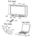
本発明の半導体装置の一例として、図16(A)にテレビジョン装置の外観図を示す。モジュールにより主画面2003が形成され、その他付属設備としてスピーカー部2009、操作スイッチなどが備えられている。筐体2001に液晶素子または発光素子を画素部に有する表示用のモジュール2002が組みこまれている。受信機2005はテレビ放送を受信するための装置である。モデム2004は、有線又は無線による通信ネットワークにテレビジョン装置を接続するための装置である。通信ネットワークに接続することにより、テレビジョン装置を用いて、双方向(視聴者から放送業者、および放送業者から視聴者)の通信をすることができる。テレビジョン装置の操作は、リモコン操作機2006、または筐体に組みこまれたスイッチを用いる。
As an example of the semiconductor device of the present invention, FIG. 16A shows an external view of a television device. A
さらに、テレビジョン装置には、主画面2003の他に、表示用モジュールでサブ画面2008を形成することができる。サブ画面2008は、チャンネルや音量などを表示するための画面として用いることができる。例えば、液晶素子を用いたモジュールで主画面2003を形成し、サブ画面2008を低消費電力で表示可能な発光素子を用いたモジュールで形成することができる。或いは、主画面2003およびサブ画面2008共に、発光素子を用いたモジュールで形成することができる。
Further, in the television device, in addition to the
図17はテレビ装置の主要な構成を示すブロック図を示している。表示用のモジュール900には、画素部921が形成されている。ソース線駆動回路922と走査線駆動回路923は、モジュール900にCOG方式により実装されている。
FIG. 17 is a block diagram illustrating a main configuration of the television device. A
その他の外部回路の構成として、映像信号の入力側では、チューナ924で受信した信号のうち、映像信号を増幅する映像信号増幅回路925と、そこから出力される信号を赤、緑、青の各色に対応した色信号に変換する映像信号処理回路926と、その映像信号をドライバICの入力仕様に変換するためのコントロール回路927などを有している。コントロール回路927は、走査線側とソース線側にそれぞれ信号を出力する。デジタル駆動する場合には、ソース線側に信号分割回路928を設け、入力デジタル信号をm個に分割して、ソース線駆動回路922に供給する構成としてもよい。
As other external circuit configurations, on the input side of the video signal, among the signals received by the
チューナ924で受信した信号のうち、音声信号は、音声信号増幅回路929に送られ、その出力は音声信号処理回路930を経てスピーカー933に供給される。制御回路931は受信局(受信周波数)や音量の制御情報を入力部932から受け、チューナ924や音声信号処理回路930に信号を送出する。
Of the signals received by the
なお、本発明はテレビジョン装置に限定されず、パーソナルコンピュータのモニタ、じめ、鉄道の駅や空港などにおける情報表示盤や、街頭における広告表示盤なども含む。 Note that the present invention is not limited to a television device, but includes a monitor of a personal computer, a starter, an information display board at a railway station or an airport, an advertisement display board at a street, and the like.
本発明の半導体装置の一例として、図16(B)に携帯電話機2301の外観図を示す。この携帯電話機2301は、表示部2302、操作部2303などを含んで構成されている。表示部2302においては、液晶素子または発光素子を用いたモジュールが用いられている。
As an example of the semiconductor device of the present invention, an external view of a
本発明の半導体装置の一例として、図16(C)に携帯型のコンピュータの外観図を示す。この携帯型のコンピュータは、本体2401、表示部2402などを含んでいる。表示部2402に、液晶素子または発光素子を用いたモジュールが用いられている。
As an example of the semiconductor device of the present invention, FIG. 16C shows an external view of a portable computer. This portable computer includes a
(実施形態5)
実施形態1、実施形態2では、基板100上に、絶縁層102、微結晶半導体層123、非晶質半導体層124、半導体層125を積層して形成する工程を説明した(図3(A)および図7(A)参照)。また、基板100を大気に曝すことなく、これらの層を積層して形成することが好ましい。このような工程を実施するためのPECVD装置の構成および使用方法について、本実施形態で説明する。
(Embodiment 5)
In Embodiments 1 and 2, the step of stacking the insulating
絶縁層102から一導電型を付与する不純物が添加された第3の半導体層105を連続成膜することが可能なPECVD装置について、図18を用いて説明する。図18はPECVD装置の上断面を示す模式図である。PECVD装置は、共通室1120の周りに、ロード室1110、アンロード室1115、4つの反応室1111〜1114を備えた構成となっている。共通室1120と各室の間にはゲートバルブ1122〜1127が備えられ、各室で行われる処理が、相互に干渉しないように構成されている。基板1130はロード室1110、アンロード室1115のカセット1128、1129に装填され、共通室1120の搬送手段1121により、各反応室1111〜1114へ運ばれる。この装置では、堆積膜の種類ごとに反応室を割り当てることが可能であり、複数の被膜を大気に触れさせることなく連続して形成することができる。
A PECVD apparatus capable of continuously forming the
各反応室1111〜1114はそれぞれ、形成する膜を限定することが好ましい。例えば、反応室1111は絶縁層102を形成する専用の室とし、反応室1112は微結晶半導体層123を形成する専用の室とし、反応室1113は非晶質半導体層124を形成する専用の室とし、反応室1114は半導体層125を形成する専用の室とする。このようにすることで、同時に絶縁層102、微結晶半導体層123、非晶質半導体層124および半導体層125を成膜することができる。その結果、量産性を高めることができる。また、ある反応室がメンテナンスやクリーニングを行っていても、他の反応室において成膜処理が可能となり、成膜処理のタクトタイムを短縮することができる。また、大気成分や大気中に浮遊する汚染不純物元素に汚染されることなく各積層界面を形成することができるので、薄膜トランジスタの電気特性のばらつきを低減することができる。
Each
また、微結晶半導体層123を形成する反応室1112は、図19のPECVD装置の反応室500が適用される。他の反応室1111、1113、1114にも、図19の反応室500を適用することができる。
Further, the
なお、図18に示すPECVD装置には、ロード室およびアンロード室が別々に設けられているが、これらを一つにしロード/アンロード室を設けてもよい。また、PECVD装置に予備室を設けてもよい。予備室で基板を予備加熱することで、各反応室において成膜までの加熱時間を短縮することが可能であるため、スループットを向上させることができる。 In the PECVD apparatus shown in FIG. 18, a load chamber and an unload chamber are provided separately, but a load / unload chamber may be provided by combining them. Further, a spare chamber may be provided in the PECVD apparatus. By preheating the substrate in the preliminary chamber, the heating time until film formation in each reaction chamber can be shortened, so that the throughput can be improved.
10 画素部
11 ソース線駆動回路
12 走査線駆動回路
13 ソース線
14 走査線
15 画素
21 スイッチングトランジスタ
22 液晶素子
23 補助容量
31 スイッチングトランジスタ
32 発光素子
33 駆動用トランジスタ
61 基板
62 基板
63 画素部
64 走査線駆動回路
65 ICチップ
66 FPC
100 基板
101 第1の導電層
102 絶縁層
103 第1の半導体層
104 第2の半導体層
104a 凹部
105、105−1、105−2 第3の半導体層
106−1、106−2 第2の導電層
108 絶縁層
109 保護層
123 微結晶半導体層
124 非晶質半導体層
125 半導体層
126 導電層
131 マスク
132 マスク
133 マスク
200 基板
201 基板
202 TFT
203 補助容量
210 走査線
211 ソース線
212 補助容量線
213 電極
214 絶縁層
215 電極
216 絶縁層
217 画素電極
220 液晶層
221 配向膜
222 配向膜
223 遮光膜
224 着色膜
225 対向電極
226 平坦化膜
300 基板
301 基板
302 TFT
303 発光素子
311 平坦化膜
312 画素電極
313 隔壁
314 発光層
315 共通電極
316 保護膜
320 樹脂層
500 反応室
501 第1の電極
502 第2の電極
503 高周波電力供給手段
504 第1の高周波電源
505 第2の高周波電源
506 第1の整合器
507 第2の整合器
508 ガス供給手段
509 排気手段
510 シリンダ
511 圧力調整弁
512 ストップバルブ
513 マスフローコントローラ
514 基板加熱ヒータ
515 ヒータコントローラ
516 絶縁材
517 バタフライバルブ
518 コンダクタンスバルブ
519 ターボ分子ポンプ
520 ドライポンプ
900 モジュール
921 画素部
922 ソース線駆動回路
923 走査線駆動回路
924 チューナ
925 映像信号増幅回路
926 映像信号処理回路
927 コントロール回路
928 信号分割回路
929 音声信号増幅回路
930 音声信号処理回路
931 制御回路
932 入力部
933 スピーカー
1110 ロード室
1111 反応室
1112 反応室
1113 反応室
1114 反応室
1115 アンロード室
1120 共通室
1121 搬送手段
1122 ゲートバルブ
1123 ゲートバルブ
1124 ゲートバルブ
1125 ゲートバルブ
1126 ゲートバルブ
1127 ゲートバルブ
1128 カセット
1130 基板
2001 筐体
2002 モジュール
2003 主画面
2004 モデム
2005 受信機
2006 リモコン操作機
2007 表示部
2008 サブ画面
2009 スピーカー部
2301 携帯電話機
2302 表示部
2303 操作部
2401 本体
2402 表示部
DESCRIPTION OF
100
203
303 Light-Emitting
Claims (1)
前記第1の導電層上方に絶縁層を形成し、
前記絶縁層上方に、微結晶半導体及びアクセプタとなる不純物元素を有し、実質的に真性である第1の半導体層と、非晶質半導体からなる第2の半導体層と、第3の半導体層と、を形成し、
前記第3の半導体層上方に第2の導電層を形成し、
前記第2の導電層をエッチングして、第3の導電層と、第4の導電層と、を形成し、
前記第3の半導体層をエッチングして、第4の半導体層と、第5の半導体層と、を形成し、
前記第3の導電層及び前記第4の導電層をエッチングする半導体装置の作製方法であって、
前記第1の半導体層の形成は、プラズマ励起化学気相成長法を用いて行い、
前記第1の半導体層の形成は、前記不純物元素を有するプロセスガスに3MHz〜30MHzと30MHz〜300MHzの2種類の高周波電力を供給することによりプラズマを生成して行い、プラズマ表面定在波効果を抑制してプラズマの均一化を図るとともにプラズマを高密度化し、結晶性の高く、膜質の良い薄膜を均一な厚さで形成し、
前記第1の導電層は、前記第1の半導体層全体と重なり、
前記第3の導電層の前記第4の導電層と対向する側の端部は、前記第4の半導体層の上面に接し、且つ、前記第4の半導体層の端部と重ならず、
前記第4の導電層の前記第3の導電層と対向する側の端部は、前記第5の半導体層の上面に接し、且つ、前記第5の半導体層の端部と重ならず、
前記第3の半導体層のエッチングの際に、前記第2の半導体層に凹部を形成することを特徴とする半導体装置の作製方法。 Forming a first conductive layer;
Forming an insulating layer above the first conductive layer;
In the insulating layer above has an impurity element which serves as a microcrystalline semiconductor and an acceptor, and a first semiconductor layer which is substantially intrinsic, and a second semiconductor layer made of amorphous semiconductor, a third semiconductor layer And form,
Forming a second conductive layer above the third semiconductor layer;
Etching the second conductive layer to form a third conductive layer and a fourth conductive layer;
Etching the third semiconductor layer to form a fourth semiconductor layer and a fifth semiconductor layer;
A method for manufacturing a semiconductor device for etching the third conductive layer and the fourth conductive layer,
The first semiconductor layer is formed using plasma enhanced chemical vapor deposition.
The first semiconductor layer is formed by generating plasma by supplying two kinds of high-frequency power of 3 MHz to 30 MHz and 30 MHz to 300 MHz to the process gas containing the impurity element, and the plasma surface standing wave effect is obtained. Suppressing and making the plasma uniform, increasing the plasma density, forming a thin film with high crystallinity and good film quality with a uniform thickness,
The first conductive layer overlaps the entire first semiconductor layer;
An end of the third conductive layer facing the fourth conductive layer is in contact with an upper surface of the fourth semiconductor layer and does not overlap with an end of the fourth semiconductor layer.
An end of the fourth conductive layer facing the third conductive layer is in contact with an upper surface of the fifth semiconductor layer and does not overlap with an end of the fifth semiconductor layer.
A method for manufacturing a semiconductor device, wherein a recess is formed in the second semiconductor layer when the third semiconductor layer is etched.
Priority Applications (1)
| Application Number | Priority Date | Filing Date | Title |
|---|---|---|---|
| JP2008204368A JP5779309B2 (en) | 2007-08-17 | 2008-08-07 | Method for manufacturing semiconductor device |
Applications Claiming Priority (3)
| Application Number | Priority Date | Filing Date | Title |
|---|---|---|---|
| JP2007213059 | 2007-08-17 | ||
| JP2007213059 | 2007-08-17 | ||
| JP2008204368A JP5779309B2 (en) | 2007-08-17 | 2008-08-07 | Method for manufacturing semiconductor device |
Publications (3)
| Publication Number | Publication Date |
|---|---|
| JP2009071288A JP2009071288A (en) | 2009-04-02 |
| JP2009071288A5 JP2009071288A5 (en) | 2011-09-15 |
| JP5779309B2 true JP5779309B2 (en) | 2015-09-16 |
Family
ID=40363289
Family Applications (1)
| Application Number | Title | Priority Date | Filing Date |
|---|---|---|---|
| JP2008204368A Expired - Fee Related JP5779309B2 (en) | 2007-08-17 | 2008-08-07 | Method for manufacturing semiconductor device |
Country Status (4)
| Country | Link |
|---|---|
| US (2) | US8101444B2 (en) |
| JP (1) | JP5779309B2 (en) |
| CN (1) | CN101409236B (en) |
| TW (1) | TWI437642B (en) |
Families Citing this family (28)
| Publication number | Priority date | Publication date | Assignee | Title |
|---|---|---|---|---|
| JP5058909B2 (en) | 2007-08-17 | 2012-10-24 | 株式会社半導体エネルギー研究所 | Plasma CVD apparatus and thin film transistor manufacturing method |
| US8101444B2 (en) | 2007-08-17 | 2012-01-24 | Semiconductor Energy Laboratory Co., Ltd. | Method for manufacturing semiconductor device |
| US7790604B2 (en) * | 2007-08-20 | 2010-09-07 | Applied Materials, Inc. | Krypton sputtering of thin tungsten layer for integrated circuits |
| US7700452B2 (en) * | 2007-08-29 | 2010-04-20 | Taiwan Semiconductor Manufacturing Company, Ltd. | Strained channel transistor |
| TWI521712B (en) * | 2007-12-03 | 2016-02-11 | 半導體能源研究所股份有限公司 | Thin film transistor, display device including thin film transistor, and method for manufacturing the same |
| JP5527966B2 (en) * | 2007-12-28 | 2014-06-25 | 株式会社半導体エネルギー研究所 | Thin film transistor |
| KR101425131B1 (en) * | 2008-01-15 | 2014-07-31 | 삼성디스플레이 주식회사 | Display substrate and display device comprising the same |
| US8247315B2 (en) * | 2008-03-17 | 2012-08-21 | Semiconductor Energy Laboratory Co., Ltd. | Plasma processing apparatus and method for manufacturing semiconductor device |
| US8530897B2 (en) * | 2008-12-11 | 2013-09-10 | Semiconductor Energy Laboratory Co., Ltd. | Display device including an inverter circuit having a microcrystalline layer |
| US20120043543A1 (en) * | 2009-04-17 | 2012-02-23 | Sharp Kabushiki Kaisha | Semiconductor device and manufacturing method therefor |
| JP4816985B2 (en) | 2009-06-16 | 2011-11-16 | Tdk株式会社 | Organic EL display device |
| CN202839621U (en) * | 2009-07-30 | 2013-03-27 | 夏普株式会社 | Thin film transistor |
| JP5419730B2 (en) * | 2010-01-27 | 2014-02-19 | 三菱電機株式会社 | Thin film transistor |
| JP5752446B2 (en) * | 2010-03-15 | 2015-07-22 | 株式会社半導体エネルギー研究所 | Semiconductor device |
| KR20110139394A (en) * | 2010-06-23 | 2011-12-29 | 주성엔지니어링(주) | Thin film transistor and method of manufacturing the same |
| US8338240B2 (en) * | 2010-10-01 | 2012-12-25 | Semiconductor Energy Laboratory Co., Ltd. | Method for manufacturing transistor |
| WO2012086481A1 (en) * | 2010-12-21 | 2012-06-28 | シャープ株式会社 | Semiconductor device and method for producing same |
| US8629445B2 (en) * | 2011-02-21 | 2014-01-14 | Semiconductor Energy Laboratory Co., Ltd. | Semiconductor device, manufacturing method thereof, and electronic appliance |
| CN103053026A (en) * | 2011-08-10 | 2013-04-17 | 松下电器产业株式会社 | Thin film transistor device and method for manufacturing thin film device |
| DE102011081648A1 (en) * | 2011-08-26 | 2013-02-28 | Krones Ag | Beer brewing process |
| JP6199583B2 (en) | 2012-04-27 | 2017-09-20 | 株式会社半導体エネルギー研究所 | Semiconductor device |
| DE112015002491T5 (en) * | 2014-05-27 | 2017-03-02 | Semiconductor Energy Laboratory Co., Ltd. | Semiconductor device and manufacturing method therefor |
| US20180274100A1 (en) * | 2017-03-24 | 2018-09-27 | Applied Materials, Inc. | Alternating between deposition and treatment of diamond-like carbon |
| US11043375B2 (en) * | 2017-08-16 | 2021-06-22 | Applied Materials, Inc. | Plasma deposition of carbon hardmask |
| WO2019199681A1 (en) | 2018-04-09 | 2019-10-17 | Applied Materials, Inc. | Carbon hard masks for patterning applications and methods related thereto |
| CN114008761A (en) | 2019-07-01 | 2022-02-01 | 应用材料公司 | Tuning film properties by optimizing plasma-coupled materials |
| US11664226B2 (en) | 2020-06-29 | 2023-05-30 | Applied Materials, Inc. | Methods for producing high-density carbon films for hardmasks and other patterning applications |
| US11664214B2 (en) | 2020-06-29 | 2023-05-30 | Applied Materials, Inc. | Methods for producing high-density, nitrogen-doped carbon films for hardmasks and other patterning applications |
Family Cites Families (66)
| Publication number | Priority date | Publication date | Assignee | Title |
|---|---|---|---|---|
| JPS56122123A (en) * | 1980-03-03 | 1981-09-25 | Shunpei Yamazaki | Semiamorphous semiconductor |
| US5091334A (en) * | 1980-03-03 | 1992-02-25 | Semiconductor Energy Laboratory Co., Ltd. | Semiconductor device |
| JPS6098680A (en) | 1983-11-04 | 1985-06-01 | Seiko Instr & Electronics Ltd | Field effect type thin film transistor |
| JPS6187371A (en) | 1984-10-05 | 1986-05-02 | Hitachi Ltd | Thin-film semiconductor device |
| US4971667A (en) * | 1988-02-05 | 1990-11-20 | Semiconductor Energy Laboratory Co., Ltd. | Plasma processing method and apparatus |
| JPH02272774A (en) * | 1989-04-14 | 1990-11-07 | Hitachi Ltd | Active matrix circuit board |
| US5084777A (en) * | 1989-11-14 | 1992-01-28 | Greyhawk Systems, Inc. | Light addressed liquid crystal light valve incorporating electrically insulating light blocking material of a-SiGe:H |
| US5256509A (en) * | 1989-11-20 | 1993-10-26 | Semiconductor Energy Laboratory Co., Ltd. | Image-forming member for electrophotography and manufacturing method for the same |
| JPH03201492A (en) * | 1989-12-28 | 1991-09-03 | Toshiba Corp | Light volume control device of laser oscillator |
| EP0473988A1 (en) | 1990-08-29 | 1992-03-11 | International Business Machines Corporation | Method of fabricating a thin film transistor having amorphous/polycrystalline semiconductor channel region |
| KR930011413B1 (en) * | 1990-09-25 | 1993-12-06 | 가부시키가이샤 한도오따이 에네루기 겐큐쇼 | Plasma cvd method for using pulsed waveform |
| US7115902B1 (en) * | 1990-11-20 | 2006-10-03 | Semiconductor Energy Laboratory Co., Ltd. | Electro-optical device and method for manufacturing the same |
| US5849601A (en) * | 1990-12-25 | 1998-12-15 | Semiconductor Energy Laboratory Co., Ltd. | Electro-optical device and method for manufacturing the same |
| JP2791422B2 (en) | 1990-12-25 | 1998-08-27 | 株式会社 半導体エネルギー研究所 | Electro-optical device and manufacturing method thereof |
| US7098479B1 (en) * | 1990-12-25 | 2006-08-29 | Semiconductor Energy Laboratory Co., Ltd. | Electro-optical device and method for manufacturing the same |
| US7576360B2 (en) * | 1990-12-25 | 2009-08-18 | Semiconductor Energy Laboratory Co., Ltd. | Electro-optical device which comprises thin film transistors and method for manufacturing the same |
| JP3255942B2 (en) * | 1991-06-19 | 2002-02-12 | 株式会社半導体エネルギー研究所 | Method for manufacturing inverted staggered thin film transistor |
| US6709907B1 (en) * | 1992-02-25 | 2004-03-23 | Semiconductor Energy Laboratory Co., Ltd. | Method of fabricating a thin film transistor |
| JP2924441B2 (en) | 1992-04-27 | 1999-07-26 | 日本電気株式会社 | Thin film transistor and method of manufacturing the same |
| JP3152829B2 (en) * | 1994-01-18 | 2001-04-03 | 株式会社東芝 | Method for manufacturing semiconductor device |
| JPH0888397A (en) * | 1994-09-16 | 1996-04-02 | Casio Comput Co Ltd | Photoelectric conversion element |
| TW303526B (en) * | 1994-12-27 | 1997-04-21 | Matsushita Electric Ind Co Ltd | |
| JPH09232235A (en) * | 1995-02-24 | 1997-09-05 | Mitsui Toatsu Chem Inc | Photoelectric conversion element |
| JP2661594B2 (en) * | 1995-05-25 | 1997-10-08 | 日本電気株式会社 | Thin film transistor and method of manufacturing the same |
| JP3220383B2 (en) * | 1996-07-23 | 2001-10-22 | 東京エレクトロン株式会社 | Plasma processing apparatus and method |
| KR100257158B1 (en) | 1997-06-30 | 2000-05-15 | 김영환 | Thin film transistor and method for manufacturing the same |
| US6197624B1 (en) * | 1997-08-29 | 2001-03-06 | Semiconductor Energy Laboratory Co., Ltd. | Method of adjusting the threshold voltage in an SOI CMOS |
| US6089191A (en) * | 1997-09-25 | 2000-07-18 | Bruce Conley | Marine habitat systems |
| US6041734A (en) * | 1997-12-01 | 2000-03-28 | Applied Materials, Inc. | Use of an asymmetric waveform to control ion bombardment during substrate processing |
| JP4293385B2 (en) * | 1998-01-27 | 2009-07-08 | 株式会社半導体エネルギー研究所 | Method for manufacturing photoelectric conversion device |
| US6849154B2 (en) * | 1998-11-27 | 2005-02-01 | Tokyo Electron Limited | Plasma etching apparatus |
| JP2001007024A (en) | 1999-06-18 | 2001-01-12 | Sanyo Electric Co Ltd | Method of forming of polycrystalline silicon film |
| JP2001077366A (en) * | 1999-08-20 | 2001-03-23 | Internatl Business Mach Corp <Ibm> | Thin film transistor, liquid crystal display device, and manufacture of thin film transistor |
| JP3538088B2 (en) | 1999-10-25 | 2004-06-14 | Nec液晶テクノロジー株式会社 | Thin film transistor and method for manufacturing the same |
| JP2001311963A (en) * | 2000-04-27 | 2001-11-09 | Toshiba Corp | Liquid crystal display device and manufacturing method therefor |
| JP3897582B2 (en) * | 2000-12-12 | 2007-03-28 | キヤノン株式会社 | Vacuum processing method, vacuum processing apparatus, semiconductor device manufacturing method, and semiconductor device |
| JP2002246605A (en) | 2001-02-20 | 2002-08-30 | Matsushita Electric Ind Co Ltd | Method of manufacturing thin film transistor for liquid crystal display device |
| TW577176B (en) * | 2003-03-31 | 2004-02-21 | Ind Tech Res Inst | Structure of thin-film transistor, and the manufacturing method thereof |
| US8319219B2 (en) * | 2003-07-14 | 2012-11-27 | Semiconductor Energy Laboratory Co., Ltd. | Light-emitting device |
| JP4748954B2 (en) | 2003-07-14 | 2011-08-17 | 株式会社半導体エネルギー研究所 | Liquid crystal display |
| JP4554292B2 (en) * | 2003-07-18 | 2010-09-29 | 株式会社半導体エネルギー研究所 | Method for manufacturing thin film transistor |
| JP2004070331A (en) * | 2003-08-01 | 2004-03-04 | Hitachi Displays Ltd | Method of manufacturing liquid crystal display |
| US7314785B2 (en) * | 2003-10-24 | 2008-01-01 | Semiconductor Energy Laboratory Co., Ltd. | Display device and manufacturing method thereof |
| JP2005167051A (en) | 2003-12-04 | 2005-06-23 | Sony Corp | Thin film transistor and manufacturing method thereof |
| US20050176188A1 (en) * | 2004-02-11 | 2005-08-11 | Fang-Chen Luo | Thin film transistor and manufacturing method thereof |
| US8058652B2 (en) * | 2004-10-28 | 2011-11-15 | Semiconductor Energy Laboratory Co., Ltd. | Semiconductor device used as electro-optical device having channel formation region containing first element, and source or drain region containing second element |
| KR100645718B1 (en) * | 2005-04-28 | 2006-11-14 | 삼성에스디아이 주식회사 | Thin Film Transistor and Method for Fabricating the Same |
| JP4577114B2 (en) | 2005-06-23 | 2010-11-10 | ソニー株式会社 | Thin film transistor manufacturing method and display device manufacturing method |
| JP2007035964A (en) | 2005-07-27 | 2007-02-08 | Sony Corp | Thin film transistor and manufacturing method thereof, and display device |
| JP2007049171A (en) | 2006-08-30 | 2007-02-22 | Chi Mei Electronics Corp | Picture display device using microcrystal thin film transistor |
| US8022466B2 (en) * | 2006-10-27 | 2011-09-20 | Macronix International Co., Ltd. | Non-volatile memory cells having a polysilicon-containing, multi-layer insulating structure, memory arrays including the same and methods of operating the same |
| JP4420032B2 (en) * | 2007-01-31 | 2010-02-24 | ソニー株式会社 | Method for manufacturing thin film semiconductor device |
| US9176353B2 (en) * | 2007-06-29 | 2015-11-03 | Semiconductor Energy Laboratory Co., Ltd. | Liquid crystal display device |
| US8921858B2 (en) * | 2007-06-29 | 2014-12-30 | Semiconductor Energy Laboratory Co., Ltd. | Light-emitting device |
| US7738050B2 (en) | 2007-07-06 | 2010-06-15 | Semiconductor Energy Laboratory Co., Ltd | Liquid crystal display device |
| JP2009049384A (en) * | 2007-07-20 | 2009-03-05 | Semiconductor Energy Lab Co Ltd | Light emitting device |
| TWI521292B (en) | 2007-07-20 | 2016-02-11 | 半導體能源研究所股份有限公司 | Liquid crystal display device |
| TWI456663B (en) | 2007-07-20 | 2014-10-11 | Semiconductor Energy Lab | Method for manufacturing display device |
| US7633089B2 (en) * | 2007-07-26 | 2009-12-15 | Semiconductor Energy Laboratory Co., Ltd. | Liquid crystal display device and electronic device provided with the same |
| US8330887B2 (en) | 2007-07-27 | 2012-12-11 | Semiconductor Energy Laboratory Co., Ltd. | Liquid crystal display device and electronic device |
| CN101765917B (en) * | 2007-08-07 | 2012-07-18 | 株式会社半导体能源研究所 | Display device and electronic device having the display device, and method for manufacturing thereof |
| JP5395382B2 (en) * | 2007-08-07 | 2014-01-22 | 株式会社半導体エネルギー研究所 | Method for manufacturing a transistor |
| JP2009071289A (en) * | 2007-08-17 | 2009-04-02 | Semiconductor Energy Lab Co Ltd | Semiconductor device, and manufacturing method thereof |
| US7611930B2 (en) * | 2007-08-17 | 2009-11-03 | Semiconductor Energy Laboratory Co., Ltd. | Method of manufacturing display device |
| US9054206B2 (en) * | 2007-08-17 | 2015-06-09 | Semiconductor Energy Laboratory Co., Ltd. | Method for manufacturing semiconductor device |
| US8101444B2 (en) | 2007-08-17 | 2012-01-24 | Semiconductor Energy Laboratory Co., Ltd. | Method for manufacturing semiconductor device |
-
2008
- 2008-08-06 US US12/222,251 patent/US8101444B2/en not_active Expired - Fee Related
- 2008-08-07 JP JP2008204368A patent/JP5779309B2/en not_active Expired - Fee Related
- 2008-08-11 CN CN2008101456976A patent/CN101409236B/en not_active Expired - Fee Related
- 2008-08-12 TW TW097130665A patent/TWI437642B/en not_active IP Right Cessation
-
2011
- 2011-12-28 US US13/338,340 patent/US8309406B2/en not_active Expired - Fee Related
Also Published As
| Publication number | Publication date |
|---|---|
| TW200913080A (en) | 2009-03-16 |
| JP2009071288A (en) | 2009-04-02 |
| US8309406B2 (en) | 2012-11-13 |
| US8101444B2 (en) | 2012-01-24 |
| TWI437642B (en) | 2014-05-11 |
| US20090047760A1 (en) | 2009-02-19 |
| CN101409236A (en) | 2009-04-15 |
| US20120094446A1 (en) | 2012-04-19 |
| CN101409236B (en) | 2012-07-11 |
Similar Documents
| Publication | Publication Date | Title |
|---|---|---|
| JP5779309B2 (en) | Method for manufacturing semiconductor device | |
| TWI487031B (en) | Semiconductor device and manufacturing method thereof | |
| JP5395382B2 (en) | Method for manufacturing a transistor | |
| JP5331407B2 (en) | Method for manufacturing semiconductor device | |
| JP5435907B2 (en) | Method for manufacturing display device | |
| JP5500803B2 (en) | Method for manufacturing thin film transistor | |
| JP5395384B2 (en) | Method for manufacturing thin film transistor | |
| JP5480480B2 (en) | Method for manufacturing semiconductor device | |
| JP5478037B2 (en) | Method for manufacturing display device | |
| US8591650B2 (en) | Method for forming crystalline semiconductor film, method for manufacturing thin film transistor, and method for manufacturing display device | |
| US8247315B2 (en) | Plasma processing apparatus and method for manufacturing semiconductor device | |
| JP2016170417A (en) | Semiconductor device | |
| JP2009071290A (en) | Method for manufacturing semiconductor device | |
| JP2009071284A (en) | Display device | |
| JP2009049384A (en) | Light emitting device |
Legal Events
| Date | Code | Title | Description |
|---|---|---|---|
| A521 | Request for written amendment filed |
Free format text: JAPANESE INTERMEDIATE CODE: A523 Effective date: 20110803 |
|
| A621 | Written request for application examination |
Free format text: JAPANESE INTERMEDIATE CODE: A621 Effective date: 20110803 |
|
| A131 | Notification of reasons for refusal |
Free format text: JAPANESE INTERMEDIATE CODE: A131 Effective date: 20130604 |
|
| A977 | Report on retrieval |
Free format text: JAPANESE INTERMEDIATE CODE: A971007 Effective date: 20130606 |
|
| A521 | Request for written amendment filed |
Free format text: JAPANESE INTERMEDIATE CODE: A523 Effective date: 20130612 |
|
| A131 | Notification of reasons for refusal |
Free format text: JAPANESE INTERMEDIATE CODE: A131 Effective date: 20131217 |
|
| A521 | Request for written amendment filed |
Free format text: JAPANESE INTERMEDIATE CODE: A523 Effective date: 20140116 |
|
| A02 | Decision of refusal |
Free format text: JAPANESE INTERMEDIATE CODE: A02 Effective date: 20140610 |
|
| A521 | Request for written amendment filed |
Free format text: JAPANESE INTERMEDIATE CODE: A523 Effective date: 20140730 |
|
| A911 | Transfer to examiner for re-examination before appeal (zenchi) |
Free format text: JAPANESE INTERMEDIATE CODE: A911 Effective date: 20140811 |
|
| A912 | Re-examination (zenchi) completed and case transferred to appeal board |
Free format text: JAPANESE INTERMEDIATE CODE: A912 Effective date: 20141010 |
|
| A521 | Request for written amendment filed |
Free format text: JAPANESE INTERMEDIATE CODE: A523 Effective date: 20150612 |
|
| A61 | First payment of annual fees (during grant procedure) |
Free format text: JAPANESE INTERMEDIATE CODE: A61 Effective date: 20150713 |
|
| R150 | Certificate of patent or registration of utility model |
Ref document number: 5779309 Country of ref document: JP Free format text: JAPANESE INTERMEDIATE CODE: R150 |
|
| R250 | Receipt of annual fees |
Free format text: JAPANESE INTERMEDIATE CODE: R250 |
|
| R250 | Receipt of annual fees |
Free format text: JAPANESE INTERMEDIATE CODE: R250 |
|
| R250 | Receipt of annual fees |
Free format text: JAPANESE INTERMEDIATE CODE: R250 |
|
| R250 | Receipt of annual fees |
Free format text: JAPANESE INTERMEDIATE CODE: R250 |
|
| LAPS | Cancellation because of no payment of annual fees |