JP5778588B2 - Removal of polymer layer in PZT array by plasma etching - Google Patents
Removal of polymer layer in PZT array by plasma etching Download PDFInfo
- Publication number
- JP5778588B2 JP5778588B2 JP2012004366A JP2012004366A JP5778588B2 JP 5778588 B2 JP5778588 B2 JP 5778588B2 JP 2012004366 A JP2012004366 A JP 2012004366A JP 2012004366 A JP2012004366 A JP 2012004366A JP 5778588 B2 JP5778588 B2 JP 5778588B2
- Authority
- JP
- Japan
- Prior art keywords
- diaphragm
- piezoelectric elements
- patterned
- openings
- gap layer
- Prior art date
- Legal status (The legal status is an assumption and is not a legal conclusion. Google has not performed a legal analysis and makes no representation as to the accuracy of the status listed.)
- Expired - Fee Related
Links
- 238000001020 plasma etching Methods 0.000 title claims description 20
- 229920000642 polymer Polymers 0.000 title description 8
- 239000000463 material Substances 0.000 claims description 66
- 239000010410 layer Substances 0.000 claims description 63
- 238000000034 method Methods 0.000 claims description 37
- 239000012790 adhesive layer Substances 0.000 claims description 30
- 238000005530 etching Methods 0.000 claims description 17
- 239000004020 conductor Substances 0.000 claims description 16
- 239000000945 filler Substances 0.000 claims description 13
- 238000000608 laser ablation Methods 0.000 claims description 7
- 238000007789 sealing Methods 0.000 claims description 6
- MYMOFIZGZYHOMD-UHFFFAOYSA-N Dioxygen Chemical compound O=O MYMOFIZGZYHOMD-UHFFFAOYSA-N 0.000 claims description 3
- 238000005520 cutting process Methods 0.000 claims description 3
- 238000000151 deposition Methods 0.000 claims description 3
- 229910001882 dioxygen Inorganic materials 0.000 claims description 3
- 239000003292 glue Substances 0.000 claims description 3
- 238000004140 cleaning Methods 0.000 claims description 2
- 238000002347 injection Methods 0.000 claims description 2
- 239000007924 injection Substances 0.000 claims description 2
- 230000008878 coupling Effects 0.000 claims 1
- 238000010168 coupling process Methods 0.000 claims 1
- 238000005859 coupling reaction Methods 0.000 claims 1
- 230000000873 masking effect Effects 0.000 claims 1
- 239000000853 adhesive Substances 0.000 description 29
- 230000001070 adhesive effect Effects 0.000 description 29
- 239000000976 ink Substances 0.000 description 22
- 238000004519 manufacturing process Methods 0.000 description 22
- 230000015572 biosynthetic process Effects 0.000 description 17
- 229910052451 lead zirconate titanate Inorganic materials 0.000 description 9
- 239000004593 Epoxy Substances 0.000 description 8
- 229920001169 thermoplastic Polymers 0.000 description 6
- 238000005516 engineering process Methods 0.000 description 5
- 238000007639 printing Methods 0.000 description 5
- 238000012545 processing Methods 0.000 description 5
- 239000004416 thermosoftening plastic Substances 0.000 description 5
- ARXHIJMGSIYYRZ-UHFFFAOYSA-N 1,2,4-trichloro-3-(3,4-dichlorophenyl)benzene Chemical compound C1=C(Cl)C(Cl)=CC=C1C1=C(Cl)C=CC(Cl)=C1Cl ARXHIJMGSIYYRZ-UHFFFAOYSA-N 0.000 description 4
- 239000004642 Polyimide Substances 0.000 description 3
- 238000013461 design Methods 0.000 description 3
- 238000005553 drilling Methods 0.000 description 3
- 239000007789 gas Substances 0.000 description 3
- 238000005040 ion trap Methods 0.000 description 3
- 239000002184 metal Substances 0.000 description 3
- 229910052751 metal Inorganic materials 0.000 description 3
- 229920001721 polyimide Polymers 0.000 description 3
- 238000007650 screen-printing Methods 0.000 description 3
- 239000007787 solid Substances 0.000 description 3
- 229920001187 thermosetting polymer Polymers 0.000 description 3
- XKRFYHLGVUSROY-UHFFFAOYSA-N Argon Chemical compound [Ar] XKRFYHLGVUSROY-UHFFFAOYSA-N 0.000 description 2
- PXHVJJICTQNCMI-UHFFFAOYSA-N Nickel Chemical compound [Ni] PXHVJJICTQNCMI-UHFFFAOYSA-N 0.000 description 2
- QVGXLLKOCUKJST-UHFFFAOYSA-N atomic oxygen Chemical compound [O] QVGXLLKOCUKJST-UHFFFAOYSA-N 0.000 description 2
- 150000001875 compounds Chemical class 0.000 description 2
- 230000008021 deposition Effects 0.000 description 2
- 238000010586 diagram Methods 0.000 description 2
- 239000003989 dielectric material Substances 0.000 description 2
- 239000000203 mixture Substances 0.000 description 2
- 239000001301 oxygen Substances 0.000 description 2
- 229910052760 oxygen Inorganic materials 0.000 description 2
- 229920002120 photoresistant polymer Polymers 0.000 description 2
- 229920000647 polyepoxide Polymers 0.000 description 2
- 239000000126 substance Substances 0.000 description 2
- 229920006259 thermoplastic polyimide Polymers 0.000 description 2
- OKTJSMMVPCPJKN-UHFFFAOYSA-N Carbon Chemical compound [C] OKTJSMMVPCPJKN-UHFFFAOYSA-N 0.000 description 1
- RYGMFSIKBFXOCR-UHFFFAOYSA-N Copper Chemical compound [Cu] RYGMFSIKBFXOCR-UHFFFAOYSA-N 0.000 description 1
- 229910018503 SF6 Inorganic materials 0.000 description 1
- BQCADISMDOOEFD-UHFFFAOYSA-N Silver Chemical compound [Ag] BQCADISMDOOEFD-UHFFFAOYSA-N 0.000 description 1
- 230000002411 adverse Effects 0.000 description 1
- 239000012080 ambient air Substances 0.000 description 1
- 229910052786 argon Inorganic materials 0.000 description 1
- 238000003491 array Methods 0.000 description 1
- 230000000712 assembly Effects 0.000 description 1
- 238000000429 assembly Methods 0.000 description 1
- 238000005452 bending Methods 0.000 description 1
- 239000003990 capacitor Substances 0.000 description 1
- 229910052799 carbon Inorganic materials 0.000 description 1
- 239000003795 chemical substances by application Substances 0.000 description 1
- 229910052802 copper Inorganic materials 0.000 description 1
- 239000010949 copper Substances 0.000 description 1
- 238000005137 deposition process Methods 0.000 description 1
- 238000001312 dry etching Methods 0.000 description 1
- 238000007772 electroless plating Methods 0.000 description 1
- 125000003700 epoxy group Chemical group 0.000 description 1
- 239000003822 epoxy resin Substances 0.000 description 1
- 239000000835 fiber Substances 0.000 description 1
- 238000007667 floating Methods 0.000 description 1
- 239000001257 hydrogen Substances 0.000 description 1
- 229910052739 hydrogen Inorganic materials 0.000 description 1
- 125000004435 hydrogen atom Chemical class [H]* 0.000 description 1
- 238000002513 implantation Methods 0.000 description 1
- 150000002500 ions Chemical class 0.000 description 1
- HFGPZNIAWCZYJU-UHFFFAOYSA-N lead zirconate titanate Chemical compound [O-2].[O-2].[O-2].[O-2].[O-2].[Ti+4].[Zr+4].[Pb+2] HFGPZNIAWCZYJU-UHFFFAOYSA-N 0.000 description 1
- 239000007788 liquid Substances 0.000 description 1
- 238000000465 moulding Methods 0.000 description 1
- 229910052759 nickel Inorganic materials 0.000 description 1
- 238000000206 photolithography Methods 0.000 description 1
- 239000004033 plastic Substances 0.000 description 1
- 239000002985 plastic film Substances 0.000 description 1
- 229920000515 polycarbonate Polymers 0.000 description 1
- 239000004417 polycarbonate Substances 0.000 description 1
- 238000003672 processing method Methods 0.000 description 1
- 229910052709 silver Inorganic materials 0.000 description 1
- 239000004332 silver Substances 0.000 description 1
- 238000010561 standard procedure Methods 0.000 description 1
- SFZCNBIFKDRMGX-UHFFFAOYSA-N sulfur hexafluoride Chemical compound FS(F)(F)(F)(F)F SFZCNBIFKDRMGX-UHFFFAOYSA-N 0.000 description 1
- 229960000909 sulfur hexafluoride Drugs 0.000 description 1
- 230000003746 surface roughness Effects 0.000 description 1
- TXEYQDLBPFQVAA-UHFFFAOYSA-N tetrafluoromethane Chemical compound FC(F)(F)F TXEYQDLBPFQVAA-UHFFFAOYSA-N 0.000 description 1
- 238000009823 thermal lamination Methods 0.000 description 1
- 238000012546 transfer Methods 0.000 description 1
Images


Classifications
-
- B—PERFORMING OPERATIONS; TRANSPORTING
- B41—PRINTING; LINING MACHINES; TYPEWRITERS; STAMPS
- B41J—TYPEWRITERS; SELECTIVE PRINTING MECHANISMS, i.e. MECHANISMS PRINTING OTHERWISE THAN FROM A FORME; CORRECTION OF TYPOGRAPHICAL ERRORS
- B41J2/00—Typewriters or selective printing mechanisms characterised by the printing or marking process for which they are designed
- B41J2/005—Typewriters or selective printing mechanisms characterised by the printing or marking process for which they are designed characterised by bringing liquid or particles selectively into contact with a printing material
- B41J2/01—Ink jet
- B41J2/135—Nozzles
- B41J2/16—Production of nozzles
- B41J2/1607—Production of print heads with piezoelectric elements
- B41J2/161—Production of print heads with piezoelectric elements of film type, deformed by bending and disposed on a diaphragm
-
- B—PERFORMING OPERATIONS; TRANSPORTING
- B41—PRINTING; LINING MACHINES; TYPEWRITERS; STAMPS
- B41J—TYPEWRITERS; SELECTIVE PRINTING MECHANISMS, i.e. MECHANISMS PRINTING OTHERWISE THAN FROM A FORME; CORRECTION OF TYPOGRAPHICAL ERRORS
- B41J2/00—Typewriters or selective printing mechanisms characterised by the printing or marking process for which they are designed
- B41J2/005—Typewriters or selective printing mechanisms characterised by the printing or marking process for which they are designed characterised by bringing liquid or particles selectively into contact with a printing material
- B41J2/01—Ink jet
- B41J2/135—Nozzles
- B41J2/16—Production of nozzles
- B41J2/1621—Manufacturing processes
- B41J2/1623—Manufacturing processes bonding and adhesion
-
- B—PERFORMING OPERATIONS; TRANSPORTING
- B41—PRINTING; LINING MACHINES; TYPEWRITERS; STAMPS
- B41J—TYPEWRITERS; SELECTIVE PRINTING MECHANISMS, i.e. MECHANISMS PRINTING OTHERWISE THAN FROM A FORME; CORRECTION OF TYPOGRAPHICAL ERRORS
- B41J2/00—Typewriters or selective printing mechanisms characterised by the printing or marking process for which they are designed
- B41J2/005—Typewriters or selective printing mechanisms characterised by the printing or marking process for which they are designed characterised by bringing liquid or particles selectively into contact with a printing material
- B41J2/01—Ink jet
- B41J2/135—Nozzles
- B41J2/16—Production of nozzles
- B41J2/1621—Manufacturing processes
- B41J2/1631—Manufacturing processes photolithography
-
- B—PERFORMING OPERATIONS; TRANSPORTING
- B41—PRINTING; LINING MACHINES; TYPEWRITERS; STAMPS
- B41J—TYPEWRITERS; SELECTIVE PRINTING MECHANISMS, i.e. MECHANISMS PRINTING OTHERWISE THAN FROM A FORME; CORRECTION OF TYPOGRAPHICAL ERRORS
- B41J2/00—Typewriters or selective printing mechanisms characterised by the printing or marking process for which they are designed
- B41J2/005—Typewriters or selective printing mechanisms characterised by the printing or marking process for which they are designed characterised by bringing liquid or particles selectively into contact with a printing material
- B41J2/01—Ink jet
- B41J2/135—Nozzles
- B41J2/16—Production of nozzles
- B41J2/1621—Manufacturing processes
- B41J2/1632—Manufacturing processes machining
- B41J2/1634—Manufacturing processes machining laser machining
-
- Y—GENERAL TAGGING OF NEW TECHNOLOGICAL DEVELOPMENTS; GENERAL TAGGING OF CROSS-SECTIONAL TECHNOLOGIES SPANNING OVER SEVERAL SECTIONS OF THE IPC; TECHNICAL SUBJECTS COVERED BY FORMER USPC CROSS-REFERENCE ART COLLECTIONS [XRACs] AND DIGESTS
- Y10—TECHNICAL SUBJECTS COVERED BY FORMER USPC
- Y10T—TECHNICAL SUBJECTS COVERED BY FORMER US CLASSIFICATION
- Y10T428/00—Stock material or miscellaneous articles
- Y10T428/31504—Composite [nonstructural laminate]
Landscapes
- Engineering & Computer Science (AREA)
- Manufacturing & Machinery (AREA)
- Physics & Mathematics (AREA)
- Optics & Photonics (AREA)
- Particle Formation And Scattering Control In Inkjet Printers (AREA)
- Micromachines (AREA)
- Drying Of Semiconductors (AREA)
Description
ドロップ・オン・デマンド・インクジェット技術は、印刷産業において広範に用いられている。ドロップ・オン・デマンド・インクジェット技術を用いるプリンタは、加熱式インクジェット技術または圧電技術を用いることができる。プリンタが加熱式インクジェットよりも製造にコストがかかるにもかかわらず、圧電式インクジェットは、概して、より幅広い種類のインクを用いることができ、コゲーションに関連する問題を取り除くことができるために好まれる。 Drop-on-demand inkjet technology is widely used in the printing industry. Printers that use drop-on-demand ink jet technology can use heated ink jet technology or piezoelectric technology. Despite the fact that printers are more costly to manufacture than heated inkjets, piezoelectric inkjets are generally preferred because they can use a wider variety of inks and eliminate problems associated with kogation. .
圧電式インクジェット印字ヘッドは、通常、たわみやすいダイアフラムと、ダイアフラムに付着した圧電素子とを含む。通常、電圧源に電気的に結合された電極との電気的接続を介して電圧を圧電素子に加えると、圧電素子は振動し、それによって、チャンバからノズルを介してたくさんのインクを放出するダイアフラムは、屈曲する。さらに、放出されたインクを交換するために、屈曲によって、インクが主なインク容器から開口部を介してチャンバに出る。 Piezoelectric ink jet print heads typically include a flexible diaphragm and a piezoelectric element attached to the diaphragm. Normally, when a voltage is applied to a piezoelectric element through an electrical connection with an electrode electrically coupled to a voltage source, the piezoelectric element vibrates, thereby releasing a large amount of ink from the chamber through the nozzle. Bend. Further, in order to replace the ejected ink, bending causes ink to exit from the main ink container through the opening into the chamber.
圧電式インクジェット技術を用いたインク・ジェット・プリンタの印刷解像度を上げることが、設計技師の目標である。圧電式インクジェット印字ヘッドのジェット密度を上げることにより、印刷解像度を上げることができる。ジェット密度を上げるための1つの方法は、ジェットスタックの内部にあるマニホールドを取り除くことである。この設計に関して、各ジェット用のジェットスタックの背部を介して単一のポートを有することが好ましい。ポートは、容器から各ジェットチャンバへのインクの移動のための通路として機能する。高密度印字ヘッドにおける多くのジェットのゆえに、多くのポート(各ジェットに対して1つ)は、ダイアフラムを介しておよび圧電素子間で垂直に通過する必要がある。 Increasing the printing resolution of ink jet printers using piezoelectric inkjet technology is the goal of design engineers. The printing resolution can be increased by increasing the jet density of the piezoelectric ink jet print head. One way to increase the jet density is to remove the manifold inside the jet stack. For this design, it is preferable to have a single port through the back of the jet stack for each jet. The port functions as a passage for the transfer of ink from the container to each jet chamber. Because of the many jets in high density printheads, many ports (one for each jet) need to pass vertically through the diaphragm and between the piezoelectric elements.
外部マニホールドを備えた高密度インクジェット印字ヘッドアセンブリの製造には、新しい処理方法が用いられる。抵抗の低い電気的接続を有する印字ヘッドの製造方法およびそれによって得られた印字ヘッドが望ましい。 New processing methods are used to manufacture high density inkjet printhead assemblies with external manifolds. A method of manufacturing a printhead having an electrical connection with low resistance and a printhead obtained thereby are desirable.
以下では、本発明の技術教示の1つまたは複数の実施形態のいくつかの態様の基本認識を提示するために、簡略化した概要を示す。この概要は、広範な概要ではなく、本開示の範囲を示すための本発明の技術教示の重要または重大な要素を識別するためのものでもない。むしろ、概要の第1目的は、後に示す詳細な説明の前置きとして簡略化した形態で1つまたは複数の構想を示すことにすぎない。 The following presents a simplified summary in order to present a basic understanding of some aspects of one or more embodiments of the technical teachings of the present invention. This summary is not an extensive overview and is not intended to identify key or critical elements of the technical teaching of the present invention in order to illustrate the scope of the disclosure. Rather, the primary purpose of the summary is merely to present one or more concepts in a simplified form as a prelude to the more detailed description that is presented later.
本発明の技術教示の一実施形態は、インクジェット印字ヘッドの形成方法を含むことができる。この方法は、ダイアフラムにダイアフラム付着材を付着させるステップであって、ダイアフラムは複数の開口部を含有できるステップと、ダイアフラムに複数の圧電素子を付着させるステップと、誘電性充填材料を供給して、複数の圧電素子を封止し、ダイアフラムと接するステップであって、ダイアフラム付着材は、ダイアフラムの複数の開口部を介して誘電性充填材料の流量を抑制するステップとを含むことができる。誘電性充填材料を硬化させ、複数の圧電素子間および複数の圧電素子の上面に、隙間層を形成できる。複数の圧電素子の上面から隙間層をプラズマエッチングによって除去できる。 One embodiment of the present teachings can include a method of forming an inkjet printhead. The method includes attaching a diaphragm adhering material to the diaphragm, the diaphragm including a plurality of openings, attaching a plurality of piezoelectric elements to the diaphragm, and supplying a dielectric filler material. Sealing the plurality of piezoelectric elements and contacting the diaphragm, wherein the diaphragm adhering material may include a step of suppressing a flow rate of the dielectric filling material through the plurality of openings of the diaphragm. The dielectric filling material is cured, and a gap layer can be formed between the plurality of piezoelectric elements and on the top surfaces of the plurality of piezoelectric elements. The gap layer can be removed from the upper surfaces of the plurality of piezoelectric elements by plasma etching.
インクジェット印字ヘッドを形成するためのもう1つの実施形態は、ダイアフラムにダイアフラム付着材を付着させるステップであって、ダイアフラムはそれらを介して複数の開口部を含むことができるステップと、ダイアフラムに複数の圧電素子を付着させるステップと、誘電性充填材料を供給して、複数の圧電素子を封止し、ダイアフラムと接するステップであって、ダイアフラム付着材は、ダイアフラムの複数の開口部を介して誘電性充填材料の流量を抑制するステップと、誘電性充填材料を硬化させ、複数の圧電素子間および複数の圧電素子の上面に、隙間層を形成するステップとを含むことができる。この方法は、さらに、パターニングされた接着層およびパターニングされた取外し可能な下地膜を隙間層の上に配置するステップであって、パターニングされた接着層とパターニングされた取外し可能な下地膜との内部の開口部は、圧電素子を覆う位置において隙間層を露出するステップと、パターニングされた取外し可能な下地膜およびパターニングされた接着層をエッチングマスクとして用いたプラズマエッチングによって、複数の圧電素子の上面から隙間層を除去するステップとを含むことができる。 Another embodiment for forming an inkjet printhead is the step of attaching a diaphragm deposit to a diaphragm, the diaphragm can include a plurality of openings therethrough, and the diaphragm includes a plurality of openings. Attaching the piezoelectric element and supplying a dielectric filling material to seal the plurality of piezoelectric elements and contact the diaphragm, wherein the diaphragm attaching material is dielectric through the openings of the diaphragm. The step of suppressing the flow rate of the filling material and the step of curing the dielectric filling material to form a gap layer between the plurality of piezoelectric elements and on the top surfaces of the plurality of piezoelectric elements can be included. The method further includes disposing a patterned adhesive layer and a patterned removable underlayer on the gap layer, the interior of the patterned adhesive layer and the patterned removable underlayer. The openings are exposed from the top surface of the plurality of piezoelectric elements by exposing the gap layer at a position covering the piezoelectric elements and performing plasma etching using the patterned removable base film and the patterned adhesive layer as an etching mask. Removing the interstitial layer.
インクジェット印字ヘッドを形成するためのもう1つの実施形態は、圧電素子層を移動キャリアに付着させるステップと、圧電素子層をダイスして、複数の圧電素子を形成するステップと、複数の圧電素子をジェットスタックサブアセンブリのダイアフラムに付着させるステップとを含むことができ、ジェットスタックサブアセンブリは、さらに、注入口/放出口板と、本体板と、ダイアフラムにおける複数の開口部と、ダイアフラムにおける複数の開口部を覆うダイアフラム付着材とを含むことができる。方法は、さらに、誘電性充填材料を供給して、複数の圧電素子を封止し、ダイアフラムと接するステップであって、ダイアフラム付着材は、ダイアフラムにおける複数の開口部を介して誘電性充填材料の流量を抑制するステップと、誘電性充填材料を硬化させ、複数の圧電素子間および複数の圧電素子の上面に隙間層を形成するステップと、隙間層の上に、パターニングされた接着層およびパターニングされた取外し可能な下地膜を配置するステップであって、パターニングされた接着層とパターニングされた取外し可能な下地膜との内部の開口部が、圧電素子を覆う位置において隙間層を露出するステップと、パターニングされた取外し可能な下地膜およびパターニングされた接着層をエッチングマスクとして用いたプラズマエッチングによって、複数の圧電素子の上面から隙間層を除去するステップであって、プラズマエッチングは、約25mTorr〜約500mTorr、例えば約100mTorr〜約200mTorrの平衡チャンバ圧力を提供するには十分な注入速度で、エッチングチャンバに酸素気体を導入するステップと、約0W〜約1000W、および特に、約800W〜約1、000W、例えば約900Wの高周波電力でプラズマを燃焼させるステップとを含むことができるステップとを含むことができる。チャンバパラメータを、例えば隙間材料(例えばエポキシの組成)に基づいて設定できる。隙間材料の組成に応じて、それらによって、または、酸素に例えばアルゴン、水素、四フッ化炭素、六フッ化硫黄とを加え組み合わせて、他のプロセスガスを用いることができる。この方法は、さらに、パターニングされた取外し可能な下地膜とパターニングされた接着層とにおける開口部内に導電性の糊状剤を配置するステップと、パターニングされた取外し可能な下地膜を除去するステップとを含むことができる。さらに、レーザービームを用いて、ダイアフラム付着材と、隙間層と、パターニングされた接着層をダイアフラムにおける複数の開口部から切除するステップであって、本体板および注入口/放出口板は、レーザービームをマスクするステップと、パターニングされた接着層を備えた隙間層にプリント回路基板(PCB)を機械的に付着させるステップであって、導電性の糊状剤は、PCB電極を圧電素子に電気的に結合させるステップと、PCBにマニホールドを付着させるステップとを含むことができる。 Another embodiment for forming an inkjet printhead includes attaching a piezoelectric element layer to a moving carrier, dicing the piezoelectric element layer to form a plurality of piezoelectric elements, and a plurality of piezoelectric elements. Attaching to the diaphragm of the jet stack subassembly, the jet stack subassembly further comprising an inlet / outlet plate, a body plate, a plurality of openings in the diaphragm, and a plurality of openings in the diaphragm. And a diaphragm adhering material covering the portion. The method further includes the step of supplying a dielectric filler material to seal the plurality of piezoelectric elements and contact the diaphragm, wherein the diaphragm adhering material is connected to the dielectric filler material through the plurality of openings in the diaphragm. Suppressing the flow rate, curing the dielectric filling material, forming a gap layer between the plurality of piezoelectric elements and on the top surface of the plurality of piezoelectric elements, and a patterned adhesive layer and patterned on the gap layer A step of disposing a removable base film, the step of exposing the gap layer at a position where an opening inside the patterned adhesive layer and the patterned removable base film covers the piezoelectric element; Plasma etching using patterned removable underlayer and patterned adhesive layer as etching mask Removing the interstitial layer from the top surface of the plurality of piezoelectric elements, wherein the plasma etch is performed at an implantation rate sufficient to provide an equilibrium chamber pressure of about 25 mTorr to about 500 mTorr, such as about 100 mTorr to about 200 mTorr. Introducing oxygen gas into the etching chamber and combusting the plasma with a high frequency power of about 0 W to about 1000 W, and particularly about 800 W to about 1,000 W, for example about 900 W. Can be included. The chamber parameters can be set, for example, based on the gap material (eg, epoxy composition). Depending on the composition of the gap material, other process gases can be used by them or in combination with oxygen, for example argon, hydrogen, carbon tetrafluoride, sulfur hexafluoride. The method further includes disposing a conductive paste within the openings in the patterned removable base film and the patterned adhesive layer, and removing the patterned removable base film. Can be included. Further, a step of cutting the diaphragm adhering material, the gap layer, and the patterned adhesive layer from a plurality of openings in the diaphragm using a laser beam, wherein the body plate and the inlet / outlet plate are And a step of mechanically attaching a printed circuit board (PCB) to a gap layer having a patterned adhesive layer, wherein the conductive glue is used to electrically connect the PCB electrode to the piezoelectric element. And attaching the manifold to the PCB.
アセンブリの形成方法は、エポキシ内の圧電性構造を封止するステップと、エポキシの少なくとも一部分をプラズマエッチングし、圧電性構造を露出させるステップとを含むことができる。 The method of forming the assembly can include sealing the piezoelectric structure in the epoxy and plasma etching at least a portion of the epoxy to expose the piezoelectric structure.
図面の細部を、いくつか簡略化し、正確な構造精度、細部、および、尺度を維持するよりもむしろ、本発明の複数の実施形態をより理解しやすいように示しているということに留意されたい。 It should be noted that several details of the drawings are shown in a simplified manner to make the embodiments of the present invention easier to understand, rather than maintaining accurate structural accuracy, details, and scale. .
ここで用いられるように、「プリンタ」という語は、デジタル複写機、製本機械、ファクシミリ装置、多機能機械などといった、目的に応じた印刷出力機能を実行する任意の装置を含む。「ポリマー」という語は、熱硬化性ポリイミド、熱可塑性樹脂、ポリカーボネート、エポキシ、および、従来技術で知られているそれらの化合物を含む長鎖分子から形成された、広範囲の炭素を含む化合物のうちのいずれかを含む。 As used herein, the term “printer” includes any device that performs a print output function depending on the purpose, such as a digital copier, bookbinding machine, facsimile machine, multi-function machine, and the like. The term “polymer” refers to a wide range of carbon-containing compounds formed from long chain molecules including thermosetting polyimides, thermoplastics, polycarbonates, epoxies, and those compounds known in the prior art. One of these.
図1の透視図では、圧電素子層10が、接着剤14を備えた移動キャリア12に取り外しできるように接合されている。圧電素子層10は、例えば、例えば約25μm〜約150μmの厚さのチタン酸ジルコン酸鉛層を含有でき、内部誘電体として機能する。圧電素子層10は、誘電性のPZTの各側面に導電素子を供給するために、両側をニッケルによって例えば無電解めっきプロセスを用いてめっきされることができる。ニッケルめっきされたPZTは、基本的に、内部PZT材料の全域における電圧電位の差を生み出す平行平板キャパシタとして機能する。キャリア12は、金属シート、プラスチックシート、または、もう1つの移動キャリアを含むことができる。圧電素子層10を移動キャリア12に付着させる接着層14は、ダイシングテープ、熱可塑性物質、または、もう1つの接着剤を含むことができる。もう1つの実施形態では、移動キャリア12は、個々の接着層14を必要としないように、糊のいらない熱可塑性層といった材料であってもよい。
In the perspective view of FIG. 1, the
図1の構造を形成した後、圧電素子層10は、図2に示したような複数の個別の圧電素子20を形成するためにダイス状に切られる。図2は圧電素子の4x3の配列を示しているが、より多くの配列を形成してもよいということを理解されたい。例えば、現在の印字ヘッドは、圧電素子の344x20の配列を有することができる。ダイス状に切ることは、ウェハーダイシングソーなどののこぎりを用いるといった機械技術、ドライエッチングプロセス、レーザーアブレーションプロセスなどを用いて行うことができる。各隣接している圧電素子20を完全に分離させるために、ダイシングプロセスは、接着剤14の一部を除去して移動キャリア12上で停止した後、または、接着剤14を介して、および、キャリア12へとダイス状に切った後終了できる。
After forming the structure of FIG. 1, the
個別の圧電素子20を形成した後、図2のアセンブリを、図3の断面図に示したようなジェットスタックサブアセンブリ30に付着させることができる。図3の断面図を、より一層詳しくするために図2の構造から拡大し、1つの部分的な圧電素子20および2つの完全な圧電素子20の断面図を示す。ジェットスタックサブアセンブリ30を、知られている技術を用いて製造できる。ジェットスタックサブアセンブリ30は、例えば、注入口/放出口板32、本体板34、および、接着性のダイアフラム付着材38を用いて本体板34に付着したダイアフラム36を含むことができる。ダイアフラム36は、以下に記載するような完成した装置においてインクを通すために、複数の開口部40を含むことができる。図3の構造は、さらに、プロセスのこの時点において周囲空気によって充填されうる複数の隙間42を含む。ダイアフラム付着材38は、ダイアフラム36を貫く開口部40が覆われるように、単一のシートポリマーといった材料の固体シートであってもよい。
After forming the individual
一実施形態では、図2の構造を、ダイアフラム36と圧電素子20との間に接着剤を用いることにより、ジェットスタックサブアセンブリ30に付着できる。例えば、測定された量の接着剤(個々に示さない)を、圧電素子20のどちらか一方の上面、ダイアフラム36、または、それらの両方に、供給、画面印刷、広げるなどすることができる。一実施形態では、各個別の圧電素子20に対して、一滴の接着剤をダイアフラム上に配置できる。接着剤の塗布後、ジェットスタックサブアセンブリ30および圧電素子20を、互いに整合し、次に、圧電素子20を接着剤によってダイアフラム36と機械的に接続する。接着剤をこの接着剤に適した技術によって硬化させ、図3の構造が得られる。
In one embodiment, the structure of FIG. 2 can be attached to the
続いて、移動キャリア12および接着剤14を、図3の構造から除去し、図4の構造が生じる。
Subsequently, the
次に、図4の構造に誘電性充填材料を供給し、次に、硬化させ、隙間層50を供給する。誘電性充填材料は、例えば、Miller‐Stephenson Chemical Co.(Danbury,CT)から市販されているEpon(商標)828エポキシ樹脂(100重量部)と、Hexion Specialty Chemicals(Columbus,OH)から市販されているEpikure(商標)3277硬化剤(49重量部)とを結合したポリマーであってもよい。誘電性充填材料を、ダイアフラム36の上面52の露出した部分を覆って、図5に示したように硬化させた後で圧電素子20を封止するには十分な量供給できる。誘電性充填材料は、さらに、図示したようにダイアフラム36内の開口部40を充填できる。ダイアフラム36において開口部40を覆うダイアフラム付着材38は、誘電性充填材料が開口部40を介して通過するのを抑制する。誘電性充填材料を硬化させる前または後に、隙間層50を平坦化できる。平坦化処理を、例えばセルフレベリング材または圧力下での機械的ワイピングおよび成形を含む技術によって行うことができる。
Next, a dielectric filler material is supplied to the structure of FIG. 4 and then cured to provide a
次に、隙間層50を圧電素子20の上面から除去する。一実施形態では、開口部62を有するパターニングされたフォトレジストマスクといったパターニングされたマスク60を、図6に示したような、知られているフォトリソグラフィの技術を用いて形成できる。開口部62は、図示したように、各圧電素子20を覆う隙間層50の一部を露出し、さらに、各圧電素子20の一部を露出している。
Next, the
もう1つの実施形態では、パターニングされたマスク60は、熱可塑性ポリイミド層であってもよい。例えば、パターニングされたマスク60は、レーザーアブレーション、穴開けプロセス、エッチングなどを用いてパターニングされるDuPont(登録商標)100ELJ層であってもよい。DuPont 100ELJは、通常、厚さ25μm(0.001インチ)で製造および供給されるが、可能な場合は例えば約20μm〜約40μmという他の厚さが適している。一実施形態では、ポリマー隙間層50の表面に、熱ラミネーションプレスを用いて、熱可塑性ポリイミドマスクを付着できる。一実施形態では、付着が、約180℃〜約200℃、例えば約190℃の温度で、生じうる。一実施形態では、付着が、約90psi〜約110psi、例えば約100psiの圧力で生じうる。付着プロセスを、持続期間約5分〜約15分、例えば約10分の間、実施できる。
In another embodiment, the patterned
一実施形態では、マスクは、隙間層50、圧電素子20、または、他の構造を持ちあげないように、またはそうでなければ損傷しないように、露出した隙間層50を十分容易に除去した後、隙間層50から出ることができる材料から形成される。プラズマエッチングといったエッチング中の温度は、150℃に達しうる。この温度によって、理論によって結び付けられることを意図せずに、マスク材料は硬化し、固くなり、高密度になりおよび/またはガスを抜くことができ、隙間層50からの除去がより困難になる。
In one embodiment, the mask is sufficiently easy to remove the exposed
マスクの開口部62を配置して、ポリマーおよび各圧電素子20の上面のみを露出することができ、各電圧阻止20の上面には、続いて例えばプリント回路基板(PCB)電極と接する銀エポキシによって、電気的接続がなされる。開口部62は、圧電素子20と続いて形成される電極との間の電気抵抗が容認可能な信頼性を有する機能素子を提供する許容限界内にあるように、十分な大きさに形成される必要がある。開口部はそれ自体、円形、楕円形、正方形、長方形などであってもよい。
A
続いて、図6の構造上において、プラズマエッチングといったエッチングが行われ、露出した隙間層50を除去する。一実施形態では、処理時間を縮小するには十分な条件下で、プラズマエッチングを実施できる。例えば、活性イオン・トラップ・プラズマ・モードを、酸素プロセスガスと組み合わせて用いることができる。例えば、酸素気体をプラズマ・エッチング・チャンバに、約100mTorr〜約200mTorr、例えば約150mTorrの平衡チャンバ圧力を供給するのに十分な注入速度で導入することができる。プラズマを、約800W〜1、000W、例えば約900Wの高周波(RF)電力で燃焼させることができる。活性イオン・エッチング・プラズマ・モードでは、図6のアセンブリを隣接している2つの活性電極間に配置できる。隣接している2つの活性電極を、2つの接地電極間に配置できる。隙間材料に応じて、エッチング時間は、約1秒〜約1時間、例えば約5分〜15分、および特に、約5分〜10分であってもよい。DuPont100ELJの25μmの厚い層を用いて、処理時間は、約1秒〜約15分、例えば約1秒〜約10分であってもよい。反応性イオンエッチング、無電子エッチング、活性エッチング、無電子イオントラップといったモードを含む、活性イオン・トラップ・モード以外のプラズマモードを、隙間材料に応じて用いることができる。モードは、プラズマチャンバにおける棚状部(つまり、活性、接地した、および、浮動型)の構成に依存している。
Subsequently, etching such as plasma etching is performed on the structure of FIG. 6 to remove the exposed
プラズマエッチングは、ニッケルめっきされたPZT圧電素子20の表面から隙間層50を効果的に除去できる。ニッケルめっきされたPZT圧電素子20の表面の表面粗さが高く、これによって、比較的深く幅の狭い(つまりアスペクト比が高い)溝からの隙間層50の除去が困難になるということが分かる。ニッケルめっきの溝に残る誘電性材料は、圧電素子20と、続いて圧電素子20と電気的に結合されるPCB電極との間の電気抵抗を増加させることができる。圧電素子20のエッチングされた表面から隙間材料50を効率的に除去することにより、抵抗が下がり、装置の電気的特性が改善される。ここに記載したようなマスクされたプラズマエッチングを用いることによって、誘電性材料は、これらの溝から従来の除去方法よりも効果的に除去される。圧電素子20内の比較的幅の狭い溝からの隙間材料50のエッチング速度は、隣接している比較的広範に間隔の開いた圧電素子20間にある隙間材料50のエッチング速度未満である。マスクされていないプラズマエッチングによって、隣接している圧電素子20間にある隙間材料50の過度の損失が生じてしまい、従って、圧電素子20を覆う位置において隙間材料50を露出し、圧電素子20間の位置において隙間材料50を保護するマスクされたプラズマエッチングを用いて、この損失を抑制することができる。
Plasma etching can effectively remove the
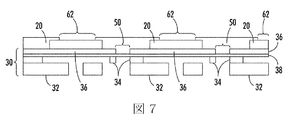
隙間層50をエッチングした後、パターニングされたマスク60を除去し、図7の構造が得られる。パターニングされたマスク60がパターニングされたフォトレジストマスクである場合、パターニングされたマスク60を、標準的な技術によって除去できる。パターニングされたマスク60がDuPont 100ELJのような熱可塑性のポリマーである場合、パターニングされたマスクを例えばピーリングによって除去できる。
After etching the
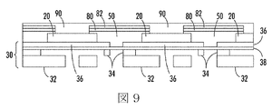
次に、パターニングされた接着層80とパターニングされた取外し可能な下地膜82とを含むアセンブリを整合し、図8に示したような図7の構造に付着させる。接着剤80は、例えば、熱硬化性または熱可塑性のシートであってもよい。取外し可能な下地膜82は、ポリイミド材料、または、接着剤80から除去できるもう1つの材料であってもよい。接着層80と取外し可能な下地膜82とを含むアセンブリは、その中に圧電素子20を露出する実施された開口部84のパターンを含む。接着剤80と下地膜82との内部の開口部84を、付着よりも前に、例えばレーザーアブレーション、穴開けプロセス、エッチングなどを用いて形成できる。開口部84の大きさを、図示したような隙間層50における開口部62の大きさに適合するように、目標とすることができる。しかし、大きさの不一致が続く処理に悪影響を及ぼさない限り、開口部がわずかに大きいまたは小さくてもよい。接着剤80と取外し可能な下地膜82との結合した厚さによって、部分的には、続く処理後に圧電素子20に残る導体の量が決定される。接着剤80と取外し可能な下地膜82との結合した厚さは、約15μm〜約100μm、または、もう1つの適切な厚さであってもよい。
Next, the assembly including the patterned
次に、図9に示したように、導電性の糊状剤といった導体90を、例えばステンシルとして取外し可能な下地膜82を用いた画面印刷プロセスによって、図8のアセンブリに塗布する。交互に、アセンブリに接着剤を供給できる。
Next, as shown in FIG. 9, a
続いて、取外し可能な下地膜82を図9の構造から、例えばピーリングによって除去することにより、図10に示した構造と同様の構造が残る。
Subsequently, the
次に、複数のビア112と複数のPCB電極114とを備えたPCB110を、接着剤80を用いて図10のアセンブリに付着させ、図11の構造が得られる。導体90は、圧電素子20をPCB電極114に電気的に結合させ、これによって、導電性パスが、PCB電極114から導体90を介して圧電素子20に伸びる。
Next, a
次に、ダイアフラム36を貫く開口部40をきれいにして、ダイアフラムを貫通してインクが通過できるようにする。開口部をきれいにするステップは、接着剤80の一部、隙間層50、および、開口部40を覆うダイアフラム付着材38を除去するステップを含む。様々な複数の実施形態では、化学的または機械的な除去技術を用いることができる。一実施形態では、自己整合除去プロセスは、図12に示したようなレーザービーム120の使用を含有でき、特に、注入口/放出口板32、本体板34、および、ダイアフラム36を金属から形成する。注入口/放出口板32、本体板34、および、適宜設計に応じてダイアフラム36は、自己整合レーザーアブレーションプロセスのためのレーザービームをマスクできる。本実施形態では、CO2レーザー、エキシマーレーザー、固体レーザー、銅蒸気レーザー、および、ファイバレーザーといったレーザーを用いることができる。CO2レーザーおよびエキシマーレーザーは、通常、エポキシ含有ポリマーを切除できる。CO2レーザーの運転費は低く、製造処理能力は高い。2つのレーザービーム120を図12に示すが、単一のレーザービームは、各穴部を、1つまたは複数のレーザーパルスを用いて順に開くことができる。もう1つの実施形態では、2つまたはそれ以上の開口部を単一の動作によって形成できる。例えば、表面にマスクを塗布でき、次に、単一の幅の広い単一のレーザービームは、単一の幅の広いレーザービームから2つ以上の開口部または全ての開口部を、1つまたは複数のパルスを用いて開くことができる。注入口/放出口板32、本体板34、および場合によってはダイアフラム36によって供給されたマスクを満たすことができるCO2レーザービームは、順次、各開口部40を照射して、ダイアフラム付着材38、隙間層50、および、接着剤80を貫く幅のある開口部を形成し、図13の構造が得られる。
Next, the
続いて、図14に示したような接着剤(個々に示さない)によって、注入口/放出口板32に開口板140を付着させることができる。開口板140は、印刷中にインクが放出されるノズル142を含む。開口板142が付着すると、ジェットスタック144は完成する。
Subsequently, the
続いて、マニホールド150をPCB110に、例えば接着剤といった液密密封接続部151を用いて接合して、図15に示したようなインクジェット印字ヘッド152が得られる。インクジェット印字ヘッド152は、多量のインクを格納するためのマニホールド150内の容器154を含むことができる。容器154からのインクを、PCB110におけるビア112を介して、ジェットスタック144内のポート156に注入する。図15は簡略化した図であり、図の左および右に付加的な構造を備えていてもよいということを理解されたい。例えば、図15には2つのポート156が示されているが、通常のジェットスタックは、例えばポートの344x20配列を有することができる。
Subsequently, the manifold 150 is joined to the
使用中に、印字ヘッド152のマニホールド150における容器154は、多量のインクを含む。印字ヘッドの最初の下塗りを用いて、インクを、容器154からPCB110のビア112を介して、ジェットスタック144のポート156を介して、および、ジェットスタック144のチャンバ158に流すことができる。各電極122に配置された電圧160に応じて、各PZT圧電素子20は、適切な時間にデジタル信号に応じて振動する。圧電素子20の振動によって、インクの滴がノズル142から放出されるチャンバ158内に圧力パルスを生み出すダイアフラム36は、屈曲する。
During use, the
従って、前述の方法および構造は、インク・ジェット・プリンタのためのジェットスタック144を形成する。一実施形態では、ジェットスタック144を、図15に示したようなインクジェット印字ヘッド152の一部として用いることができる。
Thus, the foregoing method and structure forms a
図16は、1つまたは複数の印字ヘッド154を含むプリンタ162、および、本発明の技術教示の一実施形態にかかる1つまたは複数のノズル142から噴出するインク164を示す。印字ヘッド154は、デジタル命令に従って操作され、紙シート、プラスチックなどの印刷媒体166に所望の画像を生み出す。印字ヘッド152は、スキャニング動作における印刷媒体166に関連して後ろおよび前に移動してもよく、細長い領域ごとに印刷画像を生成する。交互に、印字ヘッド154を固定してもよく、それに関連して印刷媒体166を移動してもよく、これにより、単一のパスにおける印字ヘッド154と同様に幅の広い画像を生み出す。印字ヘッド154の幅は、印刷媒体166の幅よりも狭いか、あるいは、印刷媒体と同様に幅が広い。
FIG. 16 shows a
本発明の技術教示のもう1つの実施形態は、図17に示したような圧電素子20上の隙間層50を含む図5の構造から始まる。次に、パターニングされた接着層210とパターニングされた取外し可能な下地膜212とを含むアセンブリを整合し、図17に示したような図5の構造に付着させる。パターニングされた接着層210は、例えば、熱硬化性または熱可塑性のシートであってもよい。取外し可能な下地膜212は、ポリイミド材料、または、パターニングされた接着層210から除去できるもう1つの材料であってもよい。接着層210と取外し可能な下地膜212とを含むアセンブリは、その中に、図17に示したような圧電素子20上を覆う位置にある隙間層50を露出する実施された開口部214のパターンを含む。接着剤210と下地膜212との内部の開口部214を、付着よりも前に、例えばレーザーアブレーション、穴開けプロセス、エッチングなどを用いて形成できる。接着層210と取外し可能な下地膜212との結合した厚さによって、部分的には、続く処理後に圧電素子20に残る導体の量が決定される。接着剤210と取外し可能な下地膜212との結合した厚さは、約15μm〜約100μm、または、もう1つの適切な厚さであってもよい。
Another embodiment of the technical teaching of the present invention begins with the structure of FIG. 5 including a
続いて、圧電素子20の上面を覆う隙間層50の露出した部分が、取外し可能な下地膜212および接着剤210をエッチングマスクとして用いてエッチングされ、圧電電極20を露出し、図18の構造が得られる。のプラズマエッチングのようなプラズマエッチングを、エッチング隙間層50に用いることができる。隙間層50を圧電素子20上から除去するためのプラズマエッチングを用いて、隙間層50が圧電素子20内の任意の溝から除去されることを保証する。圧電素子20の溝内に残っている任意の隙間材料50は、圧電素子20と、続いて圧電素子20を付着させるPCB電極との間の抵抗を増加させる。
Subsequently, the exposed portion of the
次に、圧電素子20上に導体230を配置し、取外し可能な下地膜212の上に配置してもよく、これによって、開口部214の完全な充填を保証する。導体は、図18の構造の表面上の画面印刷によって塗布されて図19の構造が得られる、金属充填エポキシであってもよい。画面印刷プロセスでは、取外し可能な下地膜212および接着剤210をマスクとして用いる。
Next, the
続いて、取外し可能な下地膜212を、例えば、余分な導体230を除去してもよいピーリングによって除去する。圧電素子20を、図20に示したような導体230を用いたPCB242の一部であってもよい電極240に電気的に結合でき、他方、PCB242を、接着層210によって、ジェットスタックサブアセンブリ30の隙間層50に機械的に付着させる。必要ならば導体に適した方法によって、導体230を硬化させて、図20の構造が得られる。導体230は、圧電素子20を電極240に電気的に結合させ、これにより、導電性パスが電極240から導体230を介して圧電素子20に伸びる。
Subsequently, the
続いて、ダイアフラム付着材38、隙間材料50、および、接着剤210を、例えばの複数の実施形態にかかるレーザービームによってきれいにすることができ、次に、PCB電極230を電圧160と電気的に結合することができる。電極240の電圧によって、圧電素子20は振動し、これにより、この装置は上記と同様の方法で動作できる。図20のジェットスタックを複数の実施形態によるマニホールドに付着させることができ、印字ヘッドが形成される。
Subsequently, the
上述したような圧電素子からエポキシ材料を除去するためのプラズマエッチングを、特定の複数の実施形態に加えて他の構造の形成中に実行できるということが分かるだろう。例えば、圧電性構造との接触に由来する気体または液体からの保護として、PZT圧電性構造を封止でき、固体構造との物理的な接触から損傷を抑制し、圧電性構造などに減衰を供給する。めっきされた、または、めっきされていないPZT圧電性構造を、したようなプラズマエッチングによって露出し、物理的または電気的接続地点を供給できる。 It will be appreciated that plasma etching to remove the epoxy material from the piezoelectric element as described above can be performed during the formation of other structures in addition to certain embodiments. For example, PZT piezoelectric structures can be sealed as protection from gases or liquids originating from contact with the piezoelectric structure, suppressing damage from physical contact with the solid structure and supplying attenuation to the piezoelectric structure, etc. To do. Plated or unplated PZT piezoelectric structures can be exposed by plasma etching as described to provide physical or electrical connection points.
Claims (8)
前記ダイアフラムに複数の圧電素子を付着させるステップと、
誘電性充填材料を供給して、前記複数の圧電素子を封止し、前記ダイアフラムと接するステップと、
前記誘電性充填材料を硬化させ、前記複数の圧電素子間および前記複数の圧電素子の上面に、隙間層を形成するステップと、
前記複数の圧電素子の前記上面から前記隙間層をプラズマエッチングによって除去するステップと、を含み、
前記ダイアフラムと接するステップでは、前記ダイアフラム付着材は、前記ダイアフラムの前記複数の開口部を介して前記誘電性充填材料が通過することを抑制している、インクジェット印字ヘッドの形成方法。 And steps of attaching the diaphragm attach material to the diaphragm comprising a plurality of openings,
Attaching a plurality of piezoelectric elements to the diaphragm;
By supplying a dielectric filler material, sealing the plurality of piezoelectric elements, and steps in contact with the diaphragm,
Curing the dielectric filling material, and forming a gap layer between the plurality of piezoelectric elements and on the top surface of the plurality of piezoelectric elements;
Removing the plasma etching the gap layer from said upper surface of said plurality of piezoelectric elements, only including,
In the step of contacting the diaphragm, the diaphragm adhering material suppresses the dielectric filling material from passing through the plurality of openings of the diaphragm .
前記誘電性充填材料を硬化させるステップの後、前記ダイアフラムを貫く前記複数の開口部を覆う前記ダイアフラム付着材を除去するステップと、をさらに含む、請求項1に記載の方法。 Adhering the diaphragm adhering material covering the plurality of openings through the diaphragm;
The method of claim 1, further comprising, after the step of curing the dielectric filler material, removing the diaphragm deposit covering the plurality of openings through the diaphragm.
前記ダイアフラムに複数の圧電素子を付着させるステップと、
誘電性充填材料を供給して、前記複数の圧電素子を封止し、前記ダイアフラムと接するステップと、
前記誘電性充填材料を硬化させ、前記複数の圧電素子間および前記複数の圧電素子の上面に、隙間層を形成するステップと、
パターニングされた接着層およびパターニングされた取外し可能な下地膜を前記隙間層の上に配置するステップであって、前記パターニングされた接着層と前記パターニングされた取外し可能な下地膜との内部の開口部は、前記圧電素子を覆う位置において前記隙間層を露出するステップと、
前記パターニングされた取外し可能な下地膜および前記パターニングされた接着層をエッチングマスクとして用いたプラズマエッチングによって、前記複数の圧電素子の上面から前記隙間層を除去するステップと、を含み、
前記ダイアフラムと接するステップでは、前記ダイアフラム付着材は、前記ダイアフラムの前記複数の開口部を介して前記誘電性充填材料が通過することを抑制している、インクジェット印字ヘッドの形成方法。 And steps of attaching the diaphragm attach material to said diaphragm comprising a plurality of openings through the diaphragm,
Attaching a plurality of piezoelectric elements to the diaphragm;
By supplying a dielectric filler material, sealing the plurality of piezoelectric elements, and steps in contact with the diaphragm,
Curing the dielectric filling material, and forming a gap layer between the plurality of piezoelectric elements and on the top surface of the plurality of piezoelectric elements;
Disposing a patterned adhesive layer and a patterned removable underlayer on the gap layer, the opening being within the patterned adhesive layer and the patterned removable underlayer Exposing the gap layer at a position covering the piezoelectric element;
By plasma etching using a removable base film and the patterned adhesive layer is the patterned as an etching mask, viewed including the steps of: removing the gap layer from an upper surface of the plurality of piezoelectric elements,
In the step of contacting the diaphragm, the diaphragm adhering material suppresses the dielectric filling material from passing through the plurality of openings of the diaphragm .
前記開口部に前記導体を配置した後で、前記取外し可能な下地膜を除去するステップと、
前記導体を用いて前記複数の圧電素子を複数のプリント回路基板(PCB)電極と電気的に結合するステップと、をさらに含む、請求項5に記載の方法。 Placing a conductor in the opening within the patterned adhesive layer and the patterned removable underlayer;
Removing the removable underlayer after placing the conductor in the opening; and
6. The method of claim 5, further comprising electrically coupling the plurality of piezoelectric elements with a plurality of printed circuit board (PCB) electrodes using the conductor.
前記圧電素子層をダイスして、複数の圧電素子を形成するステップと、
前記複数の圧電素子を、注入口/放出口板と、本体板と、複数の開口部を含むダイアフラムと、前記ダイアフラムにおける前記複数の開口部を覆うダイアフラム付着材とを含むジェットスタックサブアセンブリのダイアフラムに付着させるステップと、
誘電性充填材料を供給して、前記複数の圧電素子を封止し、前記ダイアフラムと接するステップと、
前記誘電性充填材料を硬化させ、前記複数の圧電素子間および前記複数の圧電素子の上面に隙間層を形成するステップと、
前記隙間層の上に、パターニングされた接着層およびパターニングされた取外し可能な下地膜を配置するステップであって、前記パターニングされた接着層と前記パターニングされた取外し可能な下地膜との内部の開口部が、前記圧電素子を覆う位置において前記隙間層を露出するステップと、
前記パターニングされた取外し可能な下地膜および前記パターニングされた接着層をエッチングマスクとして用いたプラズマエッチングによって、前記複数の圧電素子の上面から前記隙間層を除去するステップであって、前記プラズマエッチングは、100mTorr〜200mTorrの平衡チャンバ圧力を提供するには十分な注入速度で、エッチングチャンバに酸素気体を導入するステップと、800W〜1、000Wの高周波電力でプラズマを燃焼させるステップとを含むステップと、
前記パターニングされた取外し可能な下地膜と前記パターニングされた接着層とにおける前記開口部内に導電性の糊状剤を配置するステップと、
前記パターニングされた取外し可能な下地膜を除去するステップと、
レーザービームを用いて、前記ダイアフラム付着材と、前記隙間層と、前記パターニングされた接着層を前記ダイアフラムにおける前記複数の開口部から切除するステップであって、前記本体板および前記注入口/放出口板は、前記レーザービームをマスクするステップと、
前記パターニングされた接着層を備えた前記隙間層にプリント回路基板(PCB)を機械的に付着させるステップであって、前記導電性の糊状剤は、PCB電極を前記圧電素子に電気的に結合させるステップと、
前記PCBにマニホールドを付着させるステップと含み、
前記ダイアフラムと接するステップでは、前記ダイアフラム付着材は、前記ダイアフラムにおける前記複数の開口部を介して前記誘電性充填材料が通過することを抑制している、インクジェット印字ヘッドの形成方法。 Attaching the piezoelectric element layer to the moving carrier;
Dicing the piezoelectric element layer to form a plurality of piezoelectric elements;
A diaphragm of a jet stack subassembly including the plurality of piezoelectric elements, an inlet / outlet plate, a body plate, a diaphragm including a plurality of openings, and a diaphragm adhering material covering the plurality of openings in the diaphragm. and the steps to be attached to,
By supplying a dielectric filler material, sealing the plurality of piezoelectric elements, and steps in contact with the diaphragm,
Curing the dielectric filling material and forming a gap layer between the plurality of piezoelectric elements and on the top surface of the plurality of piezoelectric elements;
Disposing a patterned adhesive layer and a patterned removable underlayer on the gap layer, the openings in the patterned adhesive layer and the patterned removable underlayer; Exposing the gap layer at a position where the portion covers the piezoelectric element;
Removing the gap layer from the top surface of the plurality of piezoelectric elements by plasma etching using the patterned removable underlayer and the patterned adhesive layer as an etching mask, wherein the plasma etching comprises: Introducing oxygen gas into the etching chamber at an injection rate sufficient to provide an equilibrium chamber pressure between 100 mTorr and 200 mTorr; and burning the plasma with high frequency power between 800 W and 1,000 W;
Disposing a conductive paste in the openings in the patterned removable underlayer and the patterned adhesive layer;
Removing the patterned removable underlayer;
Cutting the diaphragm adhering material, the gap layer, and the patterned adhesive layer from the plurality of openings in the diaphragm using a laser beam, the body plate and the inlet / outlet A plate masking the laser beam;
Mechanically attaching a printed circuit board (PCB) to the gap layer with the patterned adhesive layer, wherein the conductive glue electrically couples a PCB electrode to the piezoelectric element Step to
See step and contains depositing a manifold to said PCB,
The method of forming an ink jet print head , wherein in the step of contacting the diaphragm, the diaphragm adhering material suppresses the dielectric filling material from passing through the plurality of openings in the diaphragm .
Applications Claiming Priority (2)
| Application Number | Priority Date | Filing Date | Title |
|---|---|---|---|
| US13/011,409 | 2011-01-21 | ||
| US13/011,409 US8465659B2 (en) | 2011-01-21 | 2011-01-21 | Polymer layer removal on pzt arrays using a plasma etch |
Publications (3)
| Publication Number | Publication Date |
|---|---|
| JP2012153136A JP2012153136A (en) | 2012-08-16 |
| JP2012153136A5 JP2012153136A5 (en) | 2015-02-26 |
| JP5778588B2 true JP5778588B2 (en) | 2015-09-16 |
Family
ID=46520098
Family Applications (1)
| Application Number | Title | Priority Date | Filing Date |
|---|---|---|---|
| JP2012004366A Expired - Fee Related JP5778588B2 (en) | 2011-01-21 | 2012-01-12 | Removal of polymer layer in PZT array by plasma etching |
Country Status (3)
| Country | Link |
|---|---|
| US (1) | US8465659B2 (en) |
| JP (1) | JP5778588B2 (en) |
| CN (1) | CN102602151B (en) |
Families Citing this family (5)
| Publication number | Priority date | Publication date | Assignee | Title |
|---|---|---|---|---|
| US8727508B2 (en) * | 2011-11-10 | 2014-05-20 | Xerox Corporation | Bonded silicon structure for high density print head |
| US9038269B2 (en) | 2013-04-02 | 2015-05-26 | Xerox Corporation | Printhead with nanotips for nanoscale printing and manufacturing |
| US10038267B2 (en) | 2014-06-12 | 2018-07-31 | Palo Alto Research Center Incorporated | Circuit interconnect system and method |
| US9278526B1 (en) * | 2014-10-14 | 2016-03-08 | Xerox Corporation | Modular printhead sub-assembly |
| JP2021136248A (en) * | 2020-02-21 | 2021-09-13 | 株式会社ディスコ | Processing method for device wafer |
Family Cites Families (14)
| Publication number | Priority date | Publication date | Assignee | Title |
|---|---|---|---|---|
| US5045870A (en) * | 1990-04-02 | 1991-09-03 | International Business Machines Corporation | Thermal ink drop on demand devices on a single chip with vertical integration of driver device |
| KR100481901B1 (en) * | 1999-12-10 | 2005-04-11 | 후지 샤신 필름 가부시기가이샤 | Ink jet head and printer |
| US6464324B1 (en) * | 2000-01-31 | 2002-10-15 | Picojet, Inc. | Microfluid device and ultrasonic bonding process |
| US6586112B1 (en) * | 2000-08-01 | 2003-07-01 | Hewlett-Packard Company | Mandrel and orifice plates electroformed using the same |
| CN100411872C (en) * | 2004-01-16 | 2008-08-20 | 财团法人工业技术研究院 | Ink-jet printing head and its manufacturing method |
| JP4586427B2 (en) * | 2004-06-10 | 2010-11-24 | 富士ゼロックス株式会社 | Inkjet recording head |
| US7229219B2 (en) * | 2004-09-17 | 2007-06-12 | Fujitsu Limited | Apparatuses and methods for integrating opto-electric components into the optical pathways of routing substrates with precision optical coupling and compact electrical interconnection |
| US7600863B2 (en) | 2006-01-04 | 2009-10-13 | Xerox Corporation | Inkjet jet stack external manifold |
| US7959266B2 (en) | 2007-03-28 | 2011-06-14 | Xerox Corporation | Self aligned port hole opening process for ink jet print heads |
| US8082641B2 (en) | 2007-06-01 | 2011-12-27 | Xerox Corporation | Method of manufacturing a ductile polymer-piezoelectric material composite |
| US8360557B2 (en) * | 2008-12-05 | 2013-01-29 | Xerox Corporation | Method for laser drilling fluid ports in multiple layers |
| KR101545271B1 (en) * | 2008-12-19 | 2015-08-19 | 삼성전자주식회사 | Piezoelectric acoustic transducer and method for fabricating the same |
| US8197037B2 (en) | 2009-12-15 | 2012-06-12 | Xerox Corporation | Method of removing thermoset polymer from piezoelectric transducers in a print head |
| US8303093B2 (en) * | 2009-12-15 | 2012-11-06 | Xerox Corporation | Print head having a polymer layer to facilitate assembly of the print head |
-
2011
- 2011-01-21 US US13/011,409 patent/US8465659B2/en active Active
-
2012
- 2012-01-12 JP JP2012004366A patent/JP5778588B2/en not_active Expired - Fee Related
- 2012-01-19 CN CN201210024667.6A patent/CN102602151B/en not_active Expired - Fee Related
Also Published As
| Publication number | Publication date |
|---|---|
| CN102602151B (en) | 2015-09-23 |
| CN102602151A (en) | 2012-07-25 |
| JP2012153136A (en) | 2012-08-16 |
| US8465659B2 (en) | 2013-06-18 |
| US20120187076A1 (en) | 2012-07-26 |
Similar Documents
| Publication | Publication Date | Title |
|---|---|---|
| JP4981725B2 (en) | Method for automatically forming connection holes for inkjet printheads | |
| JP5778588B2 (en) | Removal of polymer layer in PZT array by plasma etching | |
| JP5793095B2 (en) | Method for forming an inkjet printhead | |
| JP2009233927A (en) | Manufacturing method for inkjet head | |
| JP5939898B2 (en) | Planarization method of interstitial polymer using flexible flat plate | |
| CN102398423B (en) | Method of producing liquid ejection head | |
| JP5785116B2 (en) | Use of photoresist material as an interstitial fill for PZT printhead processing | |
| US8528209B2 (en) | Method for manufacturing discharge port member and method for manufacturing liquid discharge head | |
| JP2005349712A (en) | Inkjet recording head | |
| JP4755105B2 (en) | Ink jet print head and manufacturing process thereof | |
| JP5070674B2 (en) | Ink jet recording head and ink jet recording apparatus | |
| JP2010260233A (en) | Manufacturing method for liquid discharge head | |
| JP5800738B2 (en) | Inkjet print head | |
| JP6130308B2 (en) | How to make an inkjet printhead | |
| JP2006035853A (en) | Manufacturing method for inkjet recording head, inkjet recording head, substrate for recording head, and inkjet cartridge | |
| JP2012131158A (en) | Liquid ejection head manufacturing method | |
| JP2001158102A (en) | Method for manufacturing ink jet printer head | |
| JP2005219353A (en) | Nozzle plate, method of manufacturing the same, and method of manufacturing inkjet head | |
| JP2001301177A (en) | Method for manufacturing ink jet printer head | |
| JP2015051570A (en) | Inkjet head, and method for manufacturing the same | |
| JP5622653B2 (en) | Ink jet head and method of manufacturing ink jet head | |
| JP2007015341A (en) | Liquid droplet discharge head, its manufacturing method, and liquid droplet discharge apparatus | |
| JP2006168141A (en) | Inkjet recording head and manufacturing method therefor | |
| JP2007144799A (en) | Method for processing substrate, and electronic apparatus | |
| JP2005297310A (en) | Ink jet head and its manufacturing process |
Legal Events
| Date | Code | Title | Description |
|---|---|---|---|
| RD04 | Notification of resignation of power of attorney |
Free format text: JAPANESE INTERMEDIATE CODE: A7424 Effective date: 20130617 |
|
| A521 | Request for written amendment filed |
Free format text: JAPANESE INTERMEDIATE CODE: A523 Effective date: 20150108 |
|
| A621 | Written request for application examination |
Free format text: JAPANESE INTERMEDIATE CODE: A621 Effective date: 20150108 |
|
| A871 | Explanation of circumstances concerning accelerated examination |
Free format text: JAPANESE INTERMEDIATE CODE: A871 Effective date: 20150108 |
|
| A975 | Report on accelerated examination |
Free format text: JAPANESE INTERMEDIATE CODE: A971005 Effective date: 20150223 |
|
| A131 | Notification of reasons for refusal |
Free format text: JAPANESE INTERMEDIATE CODE: A131 Effective date: 20150303 |
|
| A521 | Request for written amendment filed |
Free format text: JAPANESE INTERMEDIATE CODE: A523 Effective date: 20150527 |
|
| TRDD | Decision of grant or rejection written | ||
| A01 | Written decision to grant a patent or to grant a registration (utility model) |
Free format text: JAPANESE INTERMEDIATE CODE: A01 Effective date: 20150616 |
|
| A61 | First payment of annual fees (during grant procedure) |
Free format text: JAPANESE INTERMEDIATE CODE: A61 Effective date: 20150709 |
|
| R150 | Certificate of patent or registration of utility model |
Ref document number: 5778588 Country of ref document: JP Free format text: JAPANESE INTERMEDIATE CODE: R150 |
|
| R250 | Receipt of annual fees |
Free format text: JAPANESE INTERMEDIATE CODE: R250 |
|
| R250 | Receipt of annual fees |
Free format text: JAPANESE INTERMEDIATE CODE: R250 |
|
| R250 | Receipt of annual fees |
Free format text: JAPANESE INTERMEDIATE CODE: R250 |
|
| LAPS | Cancellation because of no payment of annual fees |