JP5774570B2 - Fluorescent display tube with built-in IC for driving - Google Patents
Fluorescent display tube with built-in IC for driving Download PDFInfo
- Publication number
- JP5774570B2 JP5774570B2 JP2012241424A JP2012241424A JP5774570B2 JP 5774570 B2 JP5774570 B2 JP 5774570B2 JP 2012241424 A JP2012241424 A JP 2012241424A JP 2012241424 A JP2012241424 A JP 2012241424A JP 5774570 B2 JP5774570 B2 JP 5774570B2
- Authority
- JP
- Japan
- Prior art keywords
- filament
- support
- display tube
- fluorescent display
- driving
- Prior art date
- Legal status (The legal status is an assumption and is not a legal conclusion. Google has not performed a legal analysis and makes no representation as to the accuracy of the status listed.)
- Expired - Fee Related
Links
Images


Classifications
-
- H—ELECTRICITY
- H01—ELECTRIC ELEMENTS
- H01J—ELECTRIC DISCHARGE TUBES OR DISCHARGE LAMPS
- H01J31/00—Cathode ray tubes; Electron beam tubes
- H01J31/08—Cathode ray tubes; Electron beam tubes having a screen on or from which an image or pattern is formed, picked up, converted, or stored
- H01J31/10—Image or pattern display tubes, i.e. having electrical input and optical output; Flying-spot tubes for scanning purposes
- H01J31/12—Image or pattern display tubes, i.e. having electrical input and optical output; Flying-spot tubes for scanning purposes with luminescent screen
- H01J31/123—Flat display tubes
Description
本発明は、蛍光表示管の駆動用ICを内蔵した蛍光表示管に関し、特にその蛍光表示管のフィラメント端部支持部材の構造に関する。 The present invention relates to a fluorescent display tube having a built-in IC for driving the fluorescent display tube, and more particularly to the structure of a filament end supporting member of the fluorescent display tube.
従来駆動用ICを内蔵した蛍光表示管(駆動用IC内蔵型蛍光表示管)において、フィラメント(陰極)から放射される電子を遮蔽して駆動用ICを保護するため、フィラメント端部支持部材の押え板やサポートを遮蔽部材に用いた蛍光表示管が提案されている。
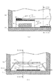
図4は、従来の押え板とサポートからなるフィラメント端部支持部を、遮蔽部材に用いた駆動用IC内蔵型蛍光表示管の断面図である。
図4(a)は、 図4(b)のX13−X13の断面図であり、図4(b)は、図4(a)のX12−X12の断面図である。
フィラメント端部支持部材は、押え板21とサポート22からなる。押え板21は、立ち上り部211、平板状部212からなり、その両端部は、外囲器を構成するアノード基板11と側面板(側面部材)12の接合部X11から外囲器の外へ引出してある。サポート22は、平板状部221、立ち上り部222、フィラメント取付け部223からなり、その平板状部221を、押え板21の平板状部212にスポット溶接してある。フィラメントFの端部は、サポート22のフィラメント取付け部223とリボン23の間に挟み、リボン23をフィラメント取付け部223にスポット溶接して固定してある。押え板21の平板状部212及びサポート22の平板状部221は、フィラメントFと駆動用IC24の間に介在して、駆動用IC24の遮蔽部材の機能も有している。なお25は、蛍光体膜を形成したアノード電極である。
In a conventional fluorescent display tube with a built-in drive IC (fluorescent display tube with a built-in drive IC), the filament end support member is pressed to protect the drive IC by shielding electrons emitted from the filament (cathode). A fluorescent display tube using a plate or a support as a shielding member has been proposed.
FIG. 4 is a cross-sectional view of a driving IC built-in type fluorescent display tube in which a filament end support portion including a conventional pressing plate and a support is used as a shielding member.
4A is a cross-sectional view taken along the line X13-X13 in FIG. 4B, and FIG. 4B is a cross-sectional view taken along the line X12-X12 in FIG. 4A.
The filament end support member includes a presser plate 21 and a
図4のフィラメント端部支持部材は、押え板21とサポート22からなり、サポート22は、立ち上り部222を備えているから、フィラメントFとアノード電極25の距離(フィラメントの高さ)が大きくなる(高くなる)。
そこでフィラメントFの高さを低くするため、フィラメント支持部のサポート22を省略して、押え板21にフィラメントFを直接取付ける構造のフィラメント端部支持部材が提案されている(例えば特許文献1)。
The filament end support member shown in FIG. 4 includes a presser plate 21 and a
Therefore, in order to reduce the height of the filament F, a filament end support member has been proposed in which the
図5は、サポートを備えないフィラメント端部支持部材を、遮蔽部材に用いた駆動用IC内蔵型蛍光表示管の断面図である。
図5(a)は、 図5(b)のX23−X23の断面図であり、図5(b)は、図5(a)のX22−X22の断面図である。
フィラメントFの端部は、サポート機能も有する押え板26の平板状部262とリボン23の間に挟み、リボン23を平板状部262にスポット溶接して固定してある。フィラメントFは、平板状部262に接触するとフィラメントFの熱が平板状部262に奪われ、いわゆるエンドクールの領域が大きくなるため、平板状部262には、フィラメントFが接触する部分にスリット(開口部)262sを櫛状に形成してある。
図5のフィラメント端部支持部材は、図4のサポートを備えていないから、その分フィラメントFの高さは、低くなる。なお261は、押え板26の立ち上り部である。
FIG. 5 is a cross-sectional view of a drive IC built-in fluorescent display tube in which a filament end supporting member without a support is used as a shielding member.
5A is a cross-sectional view taken along the line X23-X23 in FIG. 5B, and FIG. 5B is a cross-sectional view taken along the line X22-X22 in FIG. 5A.
The end of the filament F is sandwiched between the
Since the filament end portion supporting member of FIG. 5 does not include the support of FIG. 4 , the height of the filament F is reduced accordingly.
従来のサポートを省略したフィラメント端部支持部材は、フィラメントの高さを低くできるメリットがある反面問題もある。
図5の場合、押え板26は、X21部分において、アノード基板11と側面板(側面部材)12の間にガラス製の接着剤を用いて固着してあるが、X21部分におけるクラックを防止するため、熱膨張係数が接着剤に近い42−6合金を用いている。そして42−6合金は、ガラスとの接合強度を高め、気密性を高くするために水素中で加熱処理してCrの酸化皮膜を形成している。そのためフィラメントFを押え板26に直接溶接して取付けると、溶接強度が低下し好ましくない。
また図5の場合、フィラメントFの直下には、スリット262sを形成してあるから、フィラメントFから放射された電子は、スリット262sを通って駆動用IC24に到達するおそれがあり、遮蔽効果が損なわれるおそれがある。同様にして、押え板26にスリット262sを形成すると、押え板26は立体構造のため、強度的に問題が発生するおそれがある。
本発明は、従来のサポートを省略したフィラメント支持部の前記問題点に鑑み、サポートを備えたフィラメント端部支持部材を用いて、フィラメントの高さを従来のものよりも低くできる構造のフィラメント端部支持部を備えた駆動用IC内蔵型蛍光表示管を提供することを目的とする。
The filament end support member that omits the conventional support has the merit of reducing the height of the filament, but has a problem.
In the case of FIG. 5, the
In the case of FIG. 5, since the slit 262s is formed immediately below the filament F, the electrons emitted from the filament F may reach the driving
In view of the above-mentioned problem of the filament support portion in which the conventional support is omitted, the present invention provides a filament end portion having a structure in which the filament height can be made lower than that of the conventional one by using the filament end support member provided with the support. It is an object of the present invention to provide a driving IC built-in fluorescent display tube having a support portion.
請求項1に記載の駆動用IC内蔵型蛍光表示管は、気密容器内に取付けた駆動用ICをフィラメント端部支持部材で覆ってフィラメントから遮蔽する蛍光表示管において、フィラメント端部支持部材は、気密容器内に取付けた押え板とその押え板に取付けた平板状のサポートからなり、押え板は、立ち上り部と平板状部を備え、42−6合金からなり、水素中で加熱処理してCrの酸化皮膜を形成してあり、サポートは、水素中で加熱処理せずに押え板の平板状部に取付けてあり、フィラメントに対向しアンカー側を開放した櫛状のスリットを形成してあり、櫛歯相当部分を押え板の平板状部にスポット溶接してあり、フィラメントは、一端部をサポートとリボンとの間に挟みリボンをサポートにスポット溶接して固定してスリットの長手方向へ延在するように配置してあり、サポートのスリットは、フィラメントと反対の側が押え板により塞がれていることを特徴とする。
請求項2に記載の駆動用IC内蔵型蛍光表示管は、請求項1に記載の駆動用IC内蔵型蛍光表示管において、前記フィラメントは、芯線とその芯線の表面に被着した電子放出物質からなり、その電子放出物質は、芯線の端部と前記スリットの非開放側端部の間を除き芯線の表面に被着してあることを特徴とする。
請求項3に記載の駆動用IC内蔵型蛍光表示管は、請求項1又は請求項2に記載の駆動用IC内蔵型蛍光表示管において、フィラメントとアノード基板の距離は、1mm以下であることを特徴とする。
請求項4に記載の駆動用IC内蔵型蛍光表示管は、請求項1から請求項3のいずれかの請求項に記載の駆動用IC内蔵型蛍光表示管において、前記押え板は、平板状部のアンカー側端部をアノード基板側に折り曲げてあることを特徴とする。
The fluorescent display tube with built-in driving IC according to claim 1, wherein the driving IC mounted in the airtight container is covered with a filament end support member and shielded from the filament. The filament end support member is It consists of a presser plate mounted in an airtight container and a flat plate-like support attached to the presser plate. The presser plate has a rising part and a flat plate part, and is made of 42-6 alloy. The support is attached to the plate-like portion of the press plate without heat treatment in hydrogen, and has a comb-like slit that is open to the anchor side and facing the filament, The comb-equivalent portion is spot welded to the flat plate part of the presser plate, and the filament is sandwiched between the support and the ribbon and the ribbon is spot welded to the support and fixed in the longitudinal direction of the slit. The slit of the support is characterized in that the side opposite to the filament is closed by a presser plate.
The drive IC built-in fluorescent display tube according to
The drive IC built-in fluorescent display tube according to claim 3 is the drive IC built-in fluorescent display tube according to
The drive IC built-in fluorescent display tube according to claim 4 is the drive IC built-in fluorescent display tube according to any one of claims 1 to 3, wherein the presser plate is a flat portion. The anchor side end is bent to the anode substrate side.
本発明のフィラメント端部支持部材は、押え板と平板状のサポートからなり、フィラメントは、サポートの平板状部に直接固定してあるから、フィラメントFとアノード電極の距離(フィラメントの高さ)が小さく(低く)なる。
本発明のフィラメント端部支持部材のサポートには、フィラメントと対向するコ字状のスリットを形成してあるから、サポートにフィラメントの端部を直接固定しても、フィラメントがサポートに接触する範囲は狭くなり、エンドクールの領域も狭くなる。
本発明のサポートのスリットは、フィラメントと反対の側を押え板により塞いであるから、フィラメントから放射された電子がスリットを通って駆動用ICに到達することはない。即ちサポートにスリットを形成しても、フィラメント端部支持部材の遮蔽効果が損なわれることはない。
本発明のサポートは、平板状であって構造が簡単であるから、加工も簡単になり、製造コストを低減できる。また押え板は、サポートの補強材の役目もするから、サポートを薄く形成できる。
The filament end support member of the present invention comprises a holding plate and a flat plate support, and the filament is directly fixed to the flat plate portion of the support, so that the distance between the filament F and the anode electrode (filament height) is Smaller (lower).
Since the U-shaped slit facing the filament is formed on the support of the filament end support member of the present invention, even if the end of the filament is directly fixed to the support, the range where the filament contacts the support is It becomes narrower, and the end cool area becomes narrower.
Since the slit of the support according to the present invention is closed on the side opposite to the filament by a pressing plate, electrons emitted from the filament do not reach the driving IC through the slit. That is, even if a slit is formed in the support, the shielding effect of the filament end support member is not impaired.
Since the support of the present invention has a flat plate shape and a simple structure, the processing is also simplified and the manufacturing cost can be reduced. Further, since the presser plate also serves as a support reinforcing material, the support can be formed thin.
図1、図2を用いて本発明の実施例に係るフィラメント端部支持部材を備えた駆動用IC内蔵型蛍光表示管を説明する。 A driving IC built-in type fluorescent display tube equipped with a filament end supporting member according to an embodiment of the present invention will be described with reference to FIGS.
図1は、駆動用IC内蔵型蛍光表示管の一部の断面図であり、図2は、図1の一部分の拡大図である。
図1において、図1(a)は、 図1(b)のY13−Y13の断面図であり、図1(b)は、図1(a)のY12−Y12の断面図である。
蛍光表示管の外囲器(真空気密容器)は、アノード基板31、アノード基板31に対向する基板(図示せず)、両基板の間に介在する側面板(側面部材)32を低融点ガラス(フリットガラス)で接着(封着)した構造からなる。外囲器内には、電子を放出するフィラメントF(陰極)、フィラメントFから放出された電子の射突により発光する蛍光体膜を形成したアノード電極35、フィラメントFとアノード電極35の間に配設されてフィラメントFから放出された電子を制御する制御電極(図示せず)、蛍光表示管の駆動用IC34を設けてある。駆動用IC34は、ボンディングワイヤー(図示せず)によりアノード基板31上に形成された配線(図示せず)に接続されている。フィラメントFの端部は、押え板41とサポート42からなるフィラメント端部支持部材に取付け固定してある。
押え板41は、アノード基板31の内面に取り付けてあり、押え板41には、サポート42を取付け、サポート42には、フィラメントFの端部を取付け固定してある。
FIG. 1 is a cross-sectional view of a part of a fluorescent display tube with a built-in driving IC, and FIG. 2 is an enlarged view of a part of FIG.
1A is a cross-sectional view taken along the line Y13-Y13 in FIG. 1B, and FIG. 1B is a cross-sectional view taken along the line Y12-Y12 in FIG.
The envelope (vacuum hermetic container) of the fluorescent display tube is composed of an
The holding
押え板41は、アノード基板31に固定する平板状の両端部(固定部)、その両端部にそれぞれ接続した立ち上り部411、2つの立ち上がり部411の間に接続した平板状部412からなる。押え板41は、平板状部412を上底として、両端部(両端部を結んで形成される仮想線)を下底とする台形状(矩形状等でもよい)に形成している。押え板41の両端部は、アノード基板31と側面板(側面部材)32の接合部Y11から外囲器の外へ引出してある。サポート42は、平板状の部材からなり、平板状部421にスリット(開口部)421sを形成してある。スリット421sは、フィラメントF毎に設け、櫛状に形成してある。そしてスリット421sは、フィラメントFと対向し、フィラメントFの端部と反対の側(アンカー(図示せず)側で、図1(a)の場合右側)を開放して、コ字状に形成してある。
サポート42は、押え板41の平板状部412にスポット溶接してある。フィラメントFは、一端部をサポート42の平板状部421とリボン43の間に挟み、リボン43をサポート42の平板状部421にスポット溶接して固定してある。またフィラメントFの他端部は、弾性を有する金属板からなるアンカ−(図示せず)に固定してある。アンカ−は、SUS304やSUS631等のステンレス製のバネ材が用いられるのが一般的である。
なおサポート42とフィラメントFの溶接位置については、後述する。
The holding
The
The welding position between the
サポート42は、平板状であって従来のサポートのように立体構造でないから、本実施例のフィラメント端部支持部材は、フィラメントFとアノード基板31の距離(フィラメントの高さ)が小さく(低く)なる。フィラメントFとアノード基板31の距離(フィラメントの高さ)は、押え板41の立ち上り部411の高さとサポート42の平板状部421の板厚で決まるから、サポート42を用いても従来の押え板41に直接フィラメントを取付けた場合よりも、押え板41の板厚分だけ大きく(高く)なるだけである。
サポート42は、平板状であるから構造が簡単であり、またスリット421sは、プレスにより型抜きするか或いはエッチングにより形成できるから、加工が簡単になり、製造コストを低減できる。またサポート42は、スリット421sを形成しても、押え板41が補強材の役目をするから、強度が低下することはない。したがってサポート42は、薄く形成できる。
図1の駆動用IC内蔵型蛍光表示管の各部材及び部材間の寸法の一例は、次の通りである。
アノード基板31とフィラメントFの距離(アノード基板31の表面に絶縁層が形成されている場合、アノード基板31上の絶縁層とフィラメントFの距離)は1mm、アノード基板31と押え板41の下面の距離は0.6mm、押え板41の材厚(板厚)は0.2mm、サポート42の材厚(板厚)は0.1mm、駆動用ICの厚みは0.2mm(押え板41が浮き上がるので、余裕をもたせている)である。
Since the
Since the
An example of each member and the dimension between the members of the drive IC built-in fluorescent display tube of FIG. 1 is as follows.
The distance between the
図2により、フィラメントFとサポート42のスリット421sの位置関係を詳述する。
図2(a)は、押え板41、サポート42、リボン43部分の拡大平面図、図2(b)は、図2(a)のY14方向の一部分の側面図、図2(c)は、サポート42のスリット421s部分の斜視図である。
スリット421sの平面形状は、コ字状で、フィラメントFの端部或いはリボン43から遠い側(アンカー(図示せず)側)は、開放されている。フィラメントFは、スリット421sに対向し、スリット421sの長手方向へ延在するように配置してある。サポート42には、スリット421sを形成してあるから、フィラメントFを平板状のサポート42に固定しても、フィラメントFは、リボン43の近傍を除いてサポート42に接触することがない。したがってサポート42にフィラメントFの端部を直接固定しても、フィラメントFがサポート42に接触する範囲は狭くなるから、エンドクールの領域も狭くなる。
フィラメントFは、直径数μmから数十μmのタングステン等の芯線の表面に、例えばアルカリ土類金属の炭酸塩からなる電子放出物質を被着させたものである。アルカリ土類金属の炭酸塩としては、例えばBaCO3
、SrCO3 、CaCO3 を所定の配合割合で混合した三元炭酸塩が用いられる。
なお電子放出物質の被着範囲については、後述する。
The positional relationship between the filament F and the
2A is an enlarged plan view of the holding
The planar shape of the
The filament F is obtained by depositing an electron-emitting substance made of, for example, an alkaline earth metal carbonate on the surface of a core wire such as tungsten having a diameter of several μm to several tens μm. Examples of alkaline earth metal carbonates include BaCO3.
A ternary carbonate in which SrCO3 and CaCO3 are mixed at a predetermined blending ratio is used.
Note that the deposition range of the electron-emitting substance will be described later.
また押え板41の平板状部412とサポート42は、駆動用IC34を覆っているから、駆動用IC34をフィラメントFの放射電子から遮蔽する機能も有している。即ち押え板41とサポート42からなるフィラメント端部支持部材は、駆動用IC34の遮蔽部材にもなる。なおフィラメントFは、サポート42のスリット421sの長手方向(スリット421sのフィラメントFの張架方向に沿った方向であってスリット421sの開放されている部分を通る方向と定義する)に延在しているが、スリット421sのフィラメントFと反対の側は、押え板41の平板状部412により塞がれているから、フィラメントFから放射された電子がスリット421sを通って駆動用ICに到達することはない。即ちサポート42にスリット421sを形成しても、押え板41とサポート42の遮蔽効果が損なわれることはない。
Further, since the
押え板41とサポート42の材料は、従来それらに使用されている材料を使用できる。即ち押え板41には、熱膨張係数がガラス製接着剤(フリットガラス)の熱膨張係数に近い42−6合金を用い、水素中で加熱処理してCrの酸化皮膜を形成して使用する。またサポート42には、42−6合金の外、36合金、SUS430、SUS304等を用いる。それらの材料は、水素中で加熱処理せずに用いる。
As materials for the
次に図3(a)により、フィラメントFの電子放出物質の被着範囲、及びサポート42とフィラメントFの溶接位置について説明する。図3(a)は、図2(a)に対応する図である。
フィラメントFは、タングステン等の芯線Fwの表面に電子放出物質Feを被着してある。電子放出物質Feは、サポート42のスリット421sの端部(非開放側の端部)と芯線Fwの端部の間を除き、フィラメントFがスリット421sに対向する位置まで被着してある。電子放出物質Feは、最初芯線Fwの全面に被着し、後に不要部分を剥がして芯線Fwが露出するように形成してもよいし、或いは電子放出物質Feの不要部分には、最初から芯線Fwに電子放出物質Feを被着しないように形成してもよい。
サポート42等の溶接は、まずサポート42の平板状部421を押え板41の平板状部412に溶接し、次に各フィラメントFの芯線Fwの端部を、サポート42の平板状部421とリボン43の間に挟み、溶接位置43yにおいてリボン43をサポート42の平板状部421にスポット溶接してフィラメントFを挟み込んで固定してある。
またサポート42は、平板状部421のスリット421sとスリット421sの間の部分(櫛歯相当部分)を、押え板41の平板状部412にスポット溶接してある。このスポット溶接により平板状部421の櫛歯相当部分は、強度が増す。
Next, with reference to FIG. 3A, the deposition range of the electron emission material of the filament F and the welding position of the
The filament F is formed by depositing an electron emitting material Fe on the surface of a core wire Fw such as tungsten. The electron emitting material Fe is deposited to a position where the filament F faces the
In the welding of the
Further, the
次に図3(b1)、(b2)により、補強部を形成した押え板41について説明する。
図3(b1)は、図3(b2)のY16―Y16の断面図であり、図3(b2)は、図3(b1)のY15方向の側面図(アノード基板のみ断面図)である。
押え板41の平板状部412のアンカー側の端部は、アノード基板31の側に折り曲げて補強部4121を形成してある。押え板41の平板状部412は、端部を折り曲げて補強部4121を形成してあるから、強度が増し、変形し難くなる。
Next, with reference to FIGS. 3B1 and 3B2, the
3B1 is a cross-sectional view taken along the line Y16-Y16 in FIG. 3B2, and FIG. 3B2 is a side view in the Y15 direction in FIG. 3B1 (a cross-sectional view of only the anode substrate).
An end portion on the anchor side of the
31 アノード基板
32 側面板(側面部材)
34 駆動用IC
35 アノード電極
41 押え板
4121 補強部
42 サポート
421y 溶接位置
421s スリット
43y 溶接位置
43 リボン
F フィラメント(陰極)
31
34 Driving IC
35
Claims (4)
Priority Applications (4)
| Application Number | Priority Date | Filing Date | Title |
|---|---|---|---|
| JP2012241424A JP5774570B2 (en) | 2012-11-01 | 2012-11-01 | Fluorescent display tube with built-in IC for driving |
| TW102134978A TWI490906B (en) | 2012-11-01 | 2013-09-27 | Built-in driving ic type fluorescent display tube |
| US14/060,158 US9035542B2 (en) | 2012-11-01 | 2013-10-22 | Driving IC-incorporated fluorescent display device |
| PH12013000330A PH12013000330A1 (en) | 2012-11-01 | 2013-10-29 | Driving ic-incorporated fluorescent display device |
Applications Claiming Priority (1)
| Application Number | Priority Date | Filing Date | Title |
|---|---|---|---|
| JP2012241424A JP5774570B2 (en) | 2012-11-01 | 2012-11-01 | Fluorescent display tube with built-in IC for driving |
Publications (2)
| Publication Number | Publication Date |
|---|---|
| JP2014093135A JP2014093135A (en) | 2014-05-19 |
| JP5774570B2 true JP5774570B2 (en) | 2015-09-09 |
Family
ID=50546404
Family Applications (1)
| Application Number | Title | Priority Date | Filing Date |
|---|---|---|---|
| JP2012241424A Expired - Fee Related JP5774570B2 (en) | 2012-11-01 | 2012-11-01 | Fluorescent display tube with built-in IC for driving |
Country Status (4)
| Country | Link |
|---|---|
| US (1) | US9035542B2 (en) |
| JP (1) | JP5774570B2 (en) |
| PH (1) | PH12013000330A1 (en) |
| TW (1) | TWI490906B (en) |
Families Citing this family (1)
| Publication number | Priority date | Publication date | Assignee | Title |
|---|---|---|---|---|
| JP5774570B2 (en) * | 2012-11-01 | 2015-09-09 | 双葉電子工業株式会社 | Fluorescent display tube with built-in IC for driving |
Family Cites Families (11)
| Publication number | Priority date | Publication date | Assignee | Title |
|---|---|---|---|---|
| JPS6446948U (en) * | 1987-09-17 | 1989-03-23 | ||
| JP3063525B2 (en) * | 1994-06-20 | 2000-07-12 | 双葉電子工業株式会社 | Fluorescent display tube |
| JP2002063864A (en) * | 2000-08-21 | 2002-02-28 | Ise Electronics Corp | Fluorescent display tube |
| JP2002304962A (en) * | 2001-04-03 | 2002-10-18 | Futaba Corp | Fluorescent arc tube and method for manufacturing the same |
| JP4713023B2 (en) * | 2001-07-11 | 2011-06-29 | ノリタケ伊勢電子株式会社 | Fluorescent display tube |
| JP3651461B2 (en) * | 2002-09-12 | 2005-05-25 | 双葉電子工業株式会社 | Fluorescent display tube and cathode support for fluorescent display tube |
| JP4131238B2 (en) * | 2003-12-26 | 2008-08-13 | ソニー株式会社 | Display panel and display device |
| JP3929979B2 (en) * | 2004-01-20 | 2007-06-13 | 双葉電子工業株式会社 | Electron tube |
| JP4486670B2 (en) * | 2007-11-08 | 2010-06-23 | 双葉電子工業株式会社 | Fluorescent display tube |
| JP5289382B2 (en) * | 2010-05-17 | 2013-09-11 | ノリタケ伊勢電子株式会社 | Fluorescent display tube with built-in IC for driving |
| JP5774570B2 (en) * | 2012-11-01 | 2015-09-09 | 双葉電子工業株式会社 | Fluorescent display tube with built-in IC for driving |
-
2012
- 2012-11-01 JP JP2012241424A patent/JP5774570B2/en not_active Expired - Fee Related
-
2013
- 2013-09-27 TW TW102134978A patent/TWI490906B/en not_active IP Right Cessation
- 2013-10-22 US US14/060,158 patent/US9035542B2/en not_active Expired - Fee Related
- 2013-10-29 PH PH12013000330A patent/PH12013000330A1/en unknown
Also Published As
| Publication number | Publication date |
|---|---|
| TW201419359A (en) | 2014-05-16 |
| JP2014093135A (en) | 2014-05-19 |
| PH12013000330B1 (en) | 2015-05-11 |
| PH12013000330A1 (en) | 2015-05-11 |
| US9035542B2 (en) | 2015-05-19 |
| US20140117849A1 (en) | 2014-05-01 |
| TWI490906B (en) | 2015-07-01 |
Similar Documents
| Publication | Publication Date | Title |
|---|---|---|
| EP1729318B1 (en) | Vacuum vessel, its method of manufacture, and electron emission display using the vacuum vessel | |
| JP2007123268A (en) | Vacuum container, and electron emission display using it | |
| JP5774570B2 (en) | Fluorescent display tube with built-in IC for driving | |
| EP1729321A1 (en) | Electron emission display device | |
| JPH10177851A (en) | Vacuum container | |
| JP4256188B2 (en) | Flat panel display device having mesh grid | |
| EP1780751B1 (en) | Spacer and electron emission display including the spacer | |
| US7745995B2 (en) | Flat panel display having non-evaporable getter material | |
| JP2000200543A (en) | Sealed panel device and its manufacture | |
| US20050140267A1 (en) | Vacuum fluorescent display | |
| EP1780746B1 (en) | Electron emission display | |
| KR20070044577A (en) | Electron emission display device | |
| JP2005085581A (en) | Field emission display device | |
| JP2009099367A (en) | Light-emitting device | |
| JP4249842B2 (en) | Fluorescent display tube | |
| JP2006190533A (en) | Flat panel display, gate electrode structural, and its manufacturing method | |
| JP2007042480A (en) | Fluorescent display tube | |
| KR101001518B1 (en) | Flat panel display having frit | |
| JP2639211B2 (en) | Fluorescent display panel | |
| JP2007123274A (en) | Spacer and electron emission display equipped with spacer | |
| JPH025479Y2 (en) | ||
| JP2001126648A (en) | Fluorescence display | |
| KR101064451B1 (en) | Electron emission display device having getter integrated conductive mesh | |
| JP2005019119A (en) | Display device | |
| JP2006093158A (en) | Sealed panel device and its manufacturing method |
Legal Events
| Date | Code | Title | Description |
|---|---|---|---|
| A131 | Notification of reasons for refusal |
Free format text: JAPANESE INTERMEDIATE CODE: A131 Effective date: 20140415 |
|
| A521 | Request for written amendment filed |
Free format text: JAPANESE INTERMEDIATE CODE: A523 Effective date: 20140609 |
|
| A131 | Notification of reasons for refusal |
Free format text: JAPANESE INTERMEDIATE CODE: A131 Effective date: 20141111 |
|
| A521 | Request for written amendment filed |
Free format text: JAPANESE INTERMEDIATE CODE: A523 Effective date: 20150117 |
|
| TRDD | Decision of grant or rejection written | ||
| A01 | Written decision to grant a patent or to grant a registration (utility model) |
Free format text: JAPANESE INTERMEDIATE CODE: A01 Effective date: 20150623 |
|
| A61 | First payment of annual fees (during grant procedure) |
Free format text: JAPANESE INTERMEDIATE CODE: A61 Effective date: 20150701 |
|
| R150 | Certificate of patent or registration of utility model |
Ref document number: 5774570 Country of ref document: JP Free format text: JAPANESE INTERMEDIATE CODE: R150 |
|
| R250 | Receipt of annual fees |
Free format text: JAPANESE INTERMEDIATE CODE: R250 |
|
| R250 | Receipt of annual fees |
Free format text: JAPANESE INTERMEDIATE CODE: R250 |
|
| R250 | Receipt of annual fees |
Free format text: JAPANESE INTERMEDIATE CODE: R250 |
|
| LAPS | Cancellation because of no payment of annual fees |