JP5772007B2 - Light emitting device and method for manufacturing light emitting device - Google Patents
Light emitting device and method for manufacturing light emitting device Download PDFInfo
- Publication number
- JP5772007B2 JP5772007B2 JP2011012420A JP2011012420A JP5772007B2 JP 5772007 B2 JP5772007 B2 JP 5772007B2 JP 2011012420 A JP2011012420 A JP 2011012420A JP 2011012420 A JP2011012420 A JP 2011012420A JP 5772007 B2 JP5772007 B2 JP 5772007B2
- Authority
- JP
- Japan
- Prior art keywords
- light emitting
- light
- emitting element
- emitting device
- reflecting layer
- Prior art date
- Legal status (The legal status is an assumption and is not a legal conclusion. Google has not performed a legal analysis and makes no representation as to the accuracy of the status listed.)
- Active
Links
Images
Landscapes
- Led Device Packages (AREA)
Description
本発明は、発光素子がフリップチップ実装された発光装置に関する。 The present invention relates to a light emitting device in which a light emitting element is flip-chip mounted.
従来、発光素子がフリップチップ実装された発光装置において、発光素子と基板との間に反射性材料からなるアンダーフィルを注入する発明が提案された(特許文献1、2参照)。この発光装置によれば、発光素子から基板に向けて出射された光をアンダーフィルにて反射させ、発光装置を明るくできるとされる。
Conventionally, in a light-emitting device in which a light-emitting element is flip-chip mounted, inventions have been proposed in which an underfill made of a reflective material is injected between the light-emitting element and a substrate (see
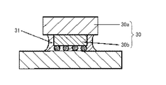
しかしながら、図9に示すように、アンダーフィル31は、発光素子30(半導体層30b、半導体層30bを成長させるための成長用基板30a)の側面に付着しやすい。このため、上記従来の発光装置では、発光素子(より具体的には、発光素子の半導体層)の側面から出射されるはずの光が、発光素子の側面に付着したアンダーフィルによって発光素子の内部へ反射されてしまい、発光素子の内部にて吸収されてしまうという問題があった。
However, as shown in FIG. 9, the
そこで、本発明は、発光素子から基板に向けて出射された光を効率よく反射させることが可能な新たな発光装置を提供することを目的とする。 In view of the above, an object of the present invention is to provide a new light-emitting device that can efficiently reflect light emitted from a light-emitting element toward a substrate.
本発明によれば、上記課題は、次の手段により解決される。 According to the present invention, the above problem is solved by the following means.
本発明は、配線が形成された基板に発光素子がフリップチップ実装された発光装置であって、前記配線上に形成された絶縁性光反射層と、前記絶縁性光反射層を貫通して前記配線に達し、前記配線と前記発光素子とを接続するバンプと、を備えることを特徴とする発光装置である。 The present invention is a light emitting device in which a light emitting element is flip-chip mounted on a substrate on which a wiring is formed, the insulating light reflecting layer formed on the wiring, and the insulating light reflecting layer penetrating the insulating light reflecting layer A light-emitting device comprising: a bump that reaches a wiring and connects the wiring and the light-emitting element.
また、本発明は、上記の発光装置において、前記発光素子と前記絶縁性光反射層との間に透明樹脂が充填されていることを特徴とする。 Moreover, the present invention is characterized in that in the above light emitting device, a transparent resin is filled between the light emitting element and the insulating light reflecting layer.
また、本発明は、上記の発光装置において、前記発光素子を封止する封止材を備え、前記封止材に蛍光体粒子が含有されていることを特徴とする。 Further, the present invention is characterized in that the above light emitting device includes a sealing material for sealing the light emitting element, and the sealing material contains phosphor particles.
また、本発明は、上記の発光装置において、前記発光素子と前記絶縁性光反射層との間に空気が充填されていることを特徴とする。 In the light emitting device according to the present invention, air is filled between the light emitting element and the insulating light reflecting layer.
また、本発明は、前記発光素子と前記絶縁性光反射層との間に前記蛍光体粒子を含有しない封止材が充填されていることを特徴とする上記の発光装置である。 Further, the present invention is the above light emitting device, wherein a sealing material not containing the phosphor particles is filled between the light emitting element and the insulating light reflecting layer.
本発明によれば、発光素子から基板に向けて出射された光を効率よく反射させることが可能な新たな発光装置を提供することができる。 ADVANTAGE OF THE INVENTION According to this invention, the new light-emitting device which can reflect the light radiate | emitted toward the board | substrate from the light emitting element efficiently can be provided.
以下に、添付した図面を参照しつつ、本発明を実施するための形態について説明する。 EMBODIMENT OF THE INVENTION Below, the form for implementing this invention is demonstrated, referring attached drawing.
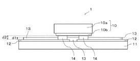
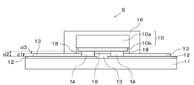
[本発明の第1実施形態に係る発光装置1]
図1は、本発明の第1実施形態に係る発光装置の断面図である。
図1に示すように、本発明の第1実施形態に係る発光装置1は、発光素子10と、配線12が形成された基板11と、絶縁性光反射層13と、バンプ14と、を備えている。以下、順に説明する。
[
FIG. 1 is a cross-sectional view of a light emitting device according to a first embodiment of the present invention.
As shown in FIG. 1, the
(発光素子10)
発光素子10としては、p電極とn電極とが同一面側に形成されたLEDチップなどを用いる。発光素子10は、半導体層10bと、半導体層10bを成長させるための成長用基板10aと、を有している。発光素子10は、配線12が形成された基板11にフリップチップ実装される。
(Light emitting element 10)
As the
(基板11)
基板11としては、樹脂やセラミック等を用いることができる。例えば、樹脂の場合は、FR−4やCEM−3等のリジット基板や、ポリエチレンテレフタレート(PET)、ポリエチレンナフタレート(PEN)、ポリイミド、液晶ポリマー、ナイロン等のフレキシブル基板、セラミックの場合は、窒化アルミニウム、アルミナ、ガラス等を用いることができる。
(Substrate 11)
As the
基板11には、配線12が形成されている。配線12としては、基板11よりも反射率が高い金属(銀メッキされた銅やアルミニウムなど)を用いる。なお、アルミニウムは銀メッキをしなくても、LEDチップから放出された光に対する反射率が高いため、低コストで基板全面の反射率を高めるに当たり、特に好ましく用いることができる。
A
(絶縁性光反射層13)
絶縁性光反射層13は、配線12上に形成される。絶縁性光反射層13としては、シリコーン樹脂と酸化チタンの粉末を混合させたものを用いる。LEDチップから放出された光に対する耐光性に優れ、反射率も高いためである。
(Insulating light reflecting layer 13)
The insulating
(バンプ14)
バンプ14は、絶縁性光反射層13を貫通して配線12に達し、配線12と発光素子10とを接続する。バンプ14は、圧接接合や超音波接合などの接合方法により、絶縁性光反射層13を突き破って絶縁性光反射層13を貫通し、配線12に達し、配線12に接続される。
(Bump 14)
The
なお、絶縁性光反射層13の厚みd1とパンプ14の高さd2との関係については、例えば次のように考える。
For example, the relationship between the thickness d1 of the insulating
すなわち、絶縁性光反射層13の厚みd1を5μmより小さくすると、発光素子10としてのLEDチップから放出された光に対する絶縁性光反射層13の反射率が低くなる。他方、絶縁性光反射層13の厚みd1を20μmより大きくすると、バンプ14によって絶縁性光反射層13を突き破りにくくなる。
That is, when the thickness d1 of the insulating
また、バンプ14の高さd2を「d1+5μm」より小さくすると、発光素子10としてのLEDチップが絶縁性光反射層13に接触するおそれがある。他方、d2を「d1+30μm」以下とすればバンプ材料のコストを抑えることができる。
If the height d2 of the
以上から、絶縁性光反射層13の厚みd1とパンプ14の高さd2との関係については、絶縁性光反射層13の厚みd1をパンプ14の高さd2より薄くすることが好ましく、さらに、絶縁性光反射層13の厚みd1を5μm〜20μmとし、バンプ14の高さd2を「d1+5μm」〜「d1+30μm」とすることがより好ましい。
From the above, regarding the relationship between the thickness d1 of the insulating
なお、超音波接合により接合すれば、バンプ14と配線12との接着強度が増す。
In addition, if it joins by ultrasonic bonding, the adhesive strength of the
本発明の第1実施形態に係る発光装置1によれば、発光素子10から基板11に向けて出射された光が絶縁性光反射層13により反射される。絶縁性光反射層13は、発光素子10に接触していないため、発光素子10の側面から出射される光を遮らない。
According to the
なお、p電極とn電極とが同一面側に形成されたGaN系の発光素子は、活性層(発光層)が発光素子の表面側に形成されていることが多い。このため、GaN系の発光素子を基板にフリップチップ実装した場合は、発光素子の活性層(発光層)が基板に接近するため、アンダーフィルが発光素子の活性層(発光層)側面に付着しやすく、活性層(発光層)から出射した光がアンダーフィルによって遮光されやすい。 In many cases, a GaN-based light emitting device in which the p electrode and the n electrode are formed on the same surface side has an active layer (light emitting layer) formed on the surface side of the light emitting device. For this reason, when a GaN-based light emitting device is flip-chip mounted on a substrate, the active layer (light emitting layer) of the light emitting device approaches the substrate, so that an underfill adheres to the side of the active layer (light emitting layer) of the light emitting device. The light emitted from the active layer (light emitting layer) is easily blocked by the underfill.
しかしながら、本発明の第1実施形態における絶縁性光反射層13は、発光素子10に接触しないため、活性層(発光層)が基板に接近するGaN系の発光素子を用いる場合であっても、発光素子10の側面から出射される光を遮らない。
However, since the insulating
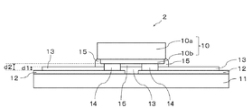
[本発明の第2実施形態に係る発光装置2]
図2は、本発明の第2実施形態に係る発光装置の断面図である。
図2に示すように、本発明の第2実施形態に係る発光装置2は、発光素子10と絶縁性光反射層13との間に透明樹脂15が充填されている点で、本発明の第1実施形態に係る発光装置1と相違する。
[
FIG. 2 is a cross-sectional view of a light emitting device according to a second embodiment of the present invention.
As shown in FIG. 2, the
発光素子10と絶縁性光反射層13との間に透明樹脂15を充填すれば、発光素子10と絶縁性光反射層13との接着強度が増す。
If the
また、発光素子10と絶縁性光反射層13との間に半導体層10bの側面を覆うように透明樹脂15を充填すれば、半導体層10bの側面に塵などが付着することを防ぐことができる。このため、発光素子10の半導体層10bから出射した光が、半導体層10bの側面に付着した塵などにより反射されることなく半導体層10bの側面から出射し、光取り出し効率が良くなる。
Moreover, if the
このような透明樹脂15の材料としては、透光性シリコーンや透光性エポキシ、例えば、信越化学株式会社のLSP−8433や稲畑産業株式会社のEH1600−G2等を用いることができる。
As a material of such a
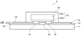
[本発明の第3実施形態に係る発光装置3]
図3は、本発明の第3実施形態に係る発光装置の断面図である。
図3に示すように、本発明の第3実施形態に係る発光装置3は、発光素子10を封止する封止材16を備え、封止材16に蛍光体粒子が含有されている点で、本発明の第1実施形態に係る発光装置1と相違する。
[
FIG. 3 is a cross-sectional view of a light emitting device according to a third embodiment of the present invention.
As shown in FIG. 3, the
本発明の第3実施形態に係る発光装置3によれば、蛍光体粒子を含有する封止材16で発光素子10が封止されるため、例えば発光素子10として青色光を発するLEDチップを用い、青色光を受けて黄色光を発する蛍光体粒子を封止材16に含有させることにより、発光素子10から出射された光を効率良く白色光に変換することができる。
According to the
封止材16は、絶縁性光反射層13や発光素子10との密着性が良好なものが好ましい。封止材16としては例えば透明樹脂を用いることができ、このような透明樹脂の材料としては、透光性シリコーンや透光性エポキシ、具体的には、信越化学株式会社のKJR−9022X−5やLPS−3419やLPS−5547、稲畑産業株式会社のEH1600−G2等が挙げられる。
The sealing
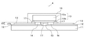
[本発明の第4実施形態に係る発光装置4]
図4は、本発明の第4実施形態に係る発光装置の断面図である。
図4に示すように、本発明の第4実施形態に係る発光装置4は、発光素子10と絶縁性光反射層13との間に空気17が充填されている点で、本発明の第3実施形態に係る発光装置3と相違する。
[
FIG. 4 is a cross-sectional view of a light emitting device according to a fourth embodiment of the present invention.
As shown in FIG. 4, the
蛍光体粒子を含有する封止材16の未硬化時の粘度を高くすれば(例えば、5万[mPa・s]以上)、発光素子10と絶縁性光反射層13との間に空気17が容易に充填されるため、本発明の第4実施形態に係る発光装置4の構成は、容易に実現することができる。
If the uncured viscosity of the sealing
発光素子10と絶縁性光反射層13との間に空気17を充填することにより、発光素子10から出た光が再び発光素子内に戻ってしまうことを防止することができる。また、樹脂等を充填しない分、部材費を低減することができる。
By filling the
発光素子10と絶縁性光反射層13との間には、上述した透明樹脂15と空気17が混在するように設けられてもよい。これにより、発光素子10と絶縁性光反射層13との接着強度が適度に増し、透明樹脂15等を完全に充填しない分、部材費を低減できる。
Between the
[本発明の第5実施形態に係る発光装置5]
図5は、本発明の第5実施形態に係る発光装置の断面図である。
図5に示すように、本発明の第5実施形態に係る発光装置5は、発光素子10と絶縁性光反射層13との間隔d3が封止材16に含有されている蛍光体粒子の直径より小さく、絶縁性光反射層13との間に蛍光体粒子を含有しない封止材18が充填されている点で、本発明の第3実施形態に係る発光装置3と相違する。
[Light Emitting Device 5 According to Fifth Embodiment of the Present Invention]
FIG. 5 is a cross-sectional view of a light emitting device according to a fifth embodiment of the present invention.
As shown in FIG. 5, in the light emitting device 5 according to the fifth embodiment of the present invention, the distance d3 between the light emitting
発光素子と絶縁性光反射層との間隔d3を封止材16に含有されている蛍光体粒子の直径より小さくすれば(例えば、直径が20μmである蛍光体粒子を用いる場合に、発光素子と絶縁性光反射層との間隔d3を10μmとする)、蛍光体粒子を含有する封止材の未硬化時の粘度を低くすることによって(例えば、5千[mPa・s]以下)、発光素子10と絶縁性光反射層13との間に蛍光体粒子を含有しない封止材18を充填することができる。
If the distance d3 between the light emitting element and the insulating light reflecting layer is made smaller than the diameter of the phosphor particles contained in the sealing material 16 (for example, when using phosphor particles having a diameter of 20 μm, The spacing d3 with the insulating light reflecting layer is set to 10 μm), and by reducing the viscosity when the sealing material containing the phosphor particles is uncured (for example, 5,000 [mPa · s] or less), the
発光素子10と絶縁性光反射層13との間に蛍光体粒子を含有しない封止材18を充填すれば、発光素子10と絶縁性光反射層13との接着強度が増す。
If the sealing
また、発光素子10の半導体層10bの側面に蛍光体粒子が存在すると、発光素子10の半導体層10bの側面から出射した光が蛍光体粒子で反射されて発光素子10の半導体層10bに戻ってしまう場合がある。
Further, when phosphor particles are present on the side surface of the
発光素子10と絶縁性光反射層13との間に半導体層10bの側面を覆うように蛍光体粒子を含有しない封止材18を充填すれば、発光素子10の半導体層10bの側面には、蛍光体粒子を含有しない封止材18が存在することとなる。このため、発光素子10の半導体層10bの側面から出射する光が、発光素子10の半導体層10bの側面に存在する蛍光体粒子で反射され半導体層10bに戻ってしまうことを防止することができる。
If the sealing
また、発光素子10と絶縁性光反射層13との間に封止材18を充填することにより、発光素子10の半導体層10bの下面から出射する光が、再び半導体層10bに戻ってしまうことを防止することができる。
Further, when the sealing
[単品、パッケージ]
以上、本発明の第1実施形態〜第5実施形態に係る発光装置1〜5について説明したが、各実施形態に係る発光装置は、個々に独立した単品として用いることもできるし、一つの基板の上に2つ以上の発光装置が実装されたパッケージとして用いることもできる。
[Single item, Package]
The light-emitting
パッケージとして用いる場合、各発光装置を配置する間隔は、50μm〜3000μmとすることが好ましい。 When used as a package, the interval between the light emitting devices is preferably 50 μm to 3000 μm.
また、パッケージとして用いる場合、絶縁性光反射層13と封止材16は、発光装置ごとに個別に形成することもできるが、2つ以上の発光装置に対して一体に形成することもできる。
Further, when used as a package, the insulating
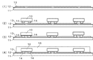
[発光装置を作製する方法の一例]
次に、本発明の第1実施形態に係る発光装置を一例として取り上げて、本発明の実施形態に係る発光装置を作製する方法の一例について説明する。
[Example of Method for Manufacturing Light-Emitting Device]
Next, taking the light emitting device according to the first embodiment of the present invention as an example, an example of a method for producing the light emitting device according to the embodiment of the present invention will be described.
図6は、本発明の第1実施形態に係る発光装置を作製する方法の一例について説明する図である。 FIG. 6 is a diagram for explaining an example of a method for producing the light emitting device according to the first embodiment of the present invention.
図6に示すように、本発明の第1実施形態に係る発光装置1は、例えば次のようにして作製することができる。
As shown in FIG. 6, the
(1)まず、バンプ14よりも厚みが薄い絶縁性光反射層13を基板11にスクリーン印刷し、硬化させる。
(2)絶縁性光反射層13を硬化した後、複数の発光素子10を所定の位置に配置する。
(3)次に、圧接接合や超音波接合などによって、発光素子10のバンプ14で絶縁性光反射層13を突き破り、発光素子10のバンプ14を絶縁性光反射層13に貫通させて配線12に接続する。
(4)そして、封止材16で発光素子10を封止する。
なお、各発光装置をパッケージではなく単品として用いる場合は、封止された複数の発光素子10を個々に切断する。
(1) First, the insulating
(2) After the insulating
(3) Next, the insulating
(4) Then, the
In addition, when using each light-emitting device as a single item instead of a package, the plurality of sealed light-emitting
以上説明した作製方法によれば、発光素子10のバンプ14で絶縁性光反射層13を突き破ることにより、発光素子10のバンプ14を絶縁性光反射層13に貫通させて、本発明の第1実施形態に係る発光装置1を容易に作製することができる。
According to the manufacturing method described above, the
以上、各実施形態について説明したが、本発明はこれらに限定されるものではなく、その趣旨を変えない範囲でさまざまに実施することができる。 As mentioned above, although each embodiment was described, this invention is not limited to these, In the range which does not change the meaning, it can implement variously.
例えば、各図面において、発光素子10の半導体層10bの幅が、半導体層10bを成長させるための成長用基板10aの幅よりも小さい場合の例を示しているが、本発明は、これに限定されるものではない。例えば、発光素子10の半導体層10bの幅と、成長用基板10aの幅とを等しくするように変形してもよい。
For example, each drawing shows an example in which the width of the
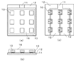
次に、本発明の第5実施形態に係る発光装置を一例として取り上げて、パッケージとしての本発明の実施形態に係る発光装置を実施例1として説明する。 Next, the light emitting device according to the fifth embodiment of the present invention will be described as an example, and the light emitting device according to the embodiment of the present invention as a package will be described as a first example.
図7は、本発明の実施例1に係るパッケージを説明する図であり、(a)は平面図、(b)は側面図、(c)は配線を強調して示す図である。 7A and 7B are diagrams for explaining a package according to the first embodiment of the present invention. FIG. 7A is a plan view, FIG. 7B is a side view, and FIG.
図7に示すように、本発明の実施例1のパッケージは、9個の発光装置を連ねたものである。 As shown in FIG. 7, the package according to the first embodiment of the present invention includes nine light emitting devices.
この場合、発光素子は3並列の3直列接続となる。絶縁性光反射層13と封止材16は、9個の発光装置に対して一体に形成している。
In this case, the light-emitting elements are connected in three parallel three series. The insulating
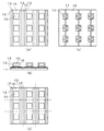
次に、本発明の第5実施形態に係る発光装置を一例として取り上げて、単品としての本発明の実施形態に係る発光装置を実施例2として説明する。 Next, the light emitting device according to the fifth embodiment of the present invention will be described as an example, and the light emitting device according to the embodiment of the present invention as a single product will be described as Example 2.
図8は、本発明の実施例2に係る発光装置を説明する図であり、(a)は平面図、(b)は側面図、(c)は配線を強調して示す図、(d)は切断の様子を示す図である。図8(d)中の破線は、切断線を示す。 8A and 8B are diagrams illustrating a light emitting device according to Example 2 of the present invention, where FIG. 8A is a plan view, FIG. 8B is a side view, FIG. FIG. 4 is a diagram showing a state of cutting. The broken line in FIG.8 (d) shows a cutting line.
図8に示すように、本発明の実施例2に係る発光装置は、9個の発光装置が連なった基板を切断線に沿って個々に切断して得られる。 As shown in FIG. 8, the light emitting device according to Example 2 of the present invention is obtained by individually cutting a substrate on which nine light emitting devices are connected along a cutting line.
以上、本発明の実施形態及び実施例について説明したが、これらの説明は、本発明の一例に関するものであり、本発明は、これらの説明によって何ら限定されるものではない。 As mentioned above, although embodiment and the Example of this invention were described, these description is related to an example of this invention, and this invention is not limited at all by these description.
1 発光装置
2 発光装置
3 発光装置
4 発光装置
5 発光装置
10 発光素子
10a 半導体層を成長させるための成長用基板
10b 半導体層
11 基板
12 配線
13 絶縁性光反射層
14 バンプ
15 透明樹脂
16 封止材
17 空気
18 蛍光体粒子を含有しない封止材
30 発光素子
30a 半導体層を成長させるための成長用基板
30b 半導体層
31 アンダーフィル
d1 絶縁性光反射層の厚み
d2 バンプの高さ
d3 発光素子と絶縁性光反射層との間隔
DESCRIPTION OF
Claims (5)
前記配線上に形成された絶縁性光反射層と、
前記絶縁性光反射層を貫通して前記配線に達し、前記配線と前記発光素子とを接続するバンプと、
前記発光素子を封止する透明樹脂と、を備え、
前記透明樹脂は、前記発光素子の周囲においては蛍光体粒子を含有し、前記発光素子と前記絶縁性光反射層との間においては蛍光体粒子を含有せず、
前記蛍光体粒子の直径は、前記発光素子と前記絶縁性光反射層との間隔よりも大きい、
ことを特徴とする発光装置。 A light-emitting device in which a light-emitting element is flip-chip mounted on a substrate on which wiring is formed,
An insulating light reflecting layer formed on the wiring;
A bump that penetrates the insulating light reflecting layer to reach the wiring, and connects the wiring and the light emitting element;
A transparent resin for sealing the light emitting element,
The transparent resin is, around the light emitting element contains the phosphor particles, in between said light emitting element insulated light reflective layer does not contain a phosphor particle,
The diameter of the phosphor particles is larger than the interval between the light emitting element and the insulating light reflecting layer.
A light emitting device characterized by that.
前記バンプで前記絶縁性光反射層を突き破り、前記絶縁性光反射層を貫通するバンプで前記発光素子を前記基板に形成された配線に接続し、
前記発光素子と前記絶縁性光反射層との間隔よりも直径の大きい蛍光体粒子を有する透明樹脂で前記配線に接続された発光素子を封止する、
ことを特徴とする発光装置の製造方法。 A light emitting element and a bump are arranged on a substrate provided with an insulating light reflecting layer on the wiring,
Breaking through the insulating light reflecting layer with the bump, connecting the light emitting element to the wiring formed on the substrate with a bump penetrating the insulating light reflecting layer,
Sealing the light emitting element connected to the wiring with a transparent resin having phosphor particles having a diameter larger than the interval between the light emitting element and the insulating light reflecting layer;
A method for manufacturing a light-emitting device.
The method for manufacturing a light emitting device according to claim 3, wherein the insulating light reflecting layer is not in contact with the light emitting element.
Priority Applications (1)
| Application Number | Priority Date | Filing Date | Title |
|---|---|---|---|
| JP2011012420A JP5772007B2 (en) | 2011-01-24 | 2011-01-24 | Light emitting device and method for manufacturing light emitting device |
Applications Claiming Priority (1)
| Application Number | Priority Date | Filing Date | Title |
|---|---|---|---|
| JP2011012420A JP5772007B2 (en) | 2011-01-24 | 2011-01-24 | Light emitting device and method for manufacturing light emitting device |
Publications (3)
| Publication Number | Publication Date |
|---|---|
| JP2012156214A JP2012156214A (en) | 2012-08-16 |
| JP2012156214A5 JP2012156214A5 (en) | 2014-03-06 |
| JP5772007B2 true JP5772007B2 (en) | 2015-09-02 |
Family
ID=46837673
Family Applications (1)
| Application Number | Title | Priority Date | Filing Date |
|---|---|---|---|
| JP2011012420A Active JP5772007B2 (en) | 2011-01-24 | 2011-01-24 | Light emitting device and method for manufacturing light emitting device |
Country Status (1)
| Country | Link |
|---|---|
| JP (1) | JP5772007B2 (en) |
Families Citing this family (4)
| Publication number | Priority date | Publication date | Assignee | Title |
|---|---|---|---|---|
| JP6116949B2 (en) * | 2013-03-14 | 2017-04-19 | 新光電気工業株式会社 | WIRING BOARD FOR MOUNTING LIGHT EMITTING ELEMENT, LIGHT EMITTING DEVICE, MANUFACTURING METHOD FOR WIRING BOARD FOR LIGHT EMITTING ELEMENT MOUNTING, AND MANUFACTURING METHOD FOR LIGHT EMITTING DEVICE |
| JP6255747B2 (en) * | 2013-07-01 | 2018-01-10 | 日亜化学工業株式会社 | Light emitting device |
| US9812625B2 (en) | 2014-02-18 | 2017-11-07 | Nichia Corporation | Light-emitting device having resin member with conductive particles |
| NL2015982B1 (en) | 2015-12-17 | 2017-07-05 | Cati B V | An electro-optical assembly. |
Family Cites Families (10)
| Publication number | Priority date | Publication date | Assignee | Title |
|---|---|---|---|---|
| JP4114364B2 (en) * | 2001-11-08 | 2008-07-09 | 日亜化学工業株式会社 | Light emitting device and manufacturing method thereof |
| US7858408B2 (en) * | 2004-11-15 | 2010-12-28 | Koninklijke Philips Electronics N.V. | LED with phosphor tile and overmolded phosphor in lens |
| JP4961887B2 (en) * | 2005-09-07 | 2012-06-27 | 豊田合成株式会社 | Solid state device |
| JP2007242820A (en) * | 2006-03-08 | 2007-09-20 | Asahi Kasei Corp | Light emitting device and light emitting device module |
| JP5053688B2 (en) * | 2007-04-09 | 2012-10-17 | 株式会社ジャパンディスプレイイースト | Light source module, light source unit, liquid crystal display device, and illumination device |
| JP4406447B2 (en) * | 2007-05-31 | 2010-01-27 | 株式会社東芝 | Optical module and manufacturing method thereof |
| CN101679613A (en) * | 2007-06-15 | 2010-03-24 | 积水化学工业株式会社 | Sealing agent for optical semiconductor element and optical semiconductor element |
| JP2009135484A (en) * | 2007-11-09 | 2009-06-18 | Hitachi Chem Co Ltd | Optical semiconductor device |
| JP2010199105A (en) * | 2009-02-23 | 2010-09-09 | Stanley Electric Co Ltd | Light-emitting device and method of manufacturing the same |
| JP5144578B2 (en) * | 2009-03-31 | 2013-02-13 | 豊田合成株式会社 | Method for manufacturing light emitting device |
-
2011
- 2011-01-24 JP JP2011012420A patent/JP5772007B2/en active Active
Also Published As
| Publication number | Publication date |
|---|---|
| JP2012156214A (en) | 2012-08-16 |
Similar Documents
| Publication | Publication Date | Title |
|---|---|---|
| JP6398222B2 (en) | Light emitting device and manufacturing method thereof | |
| JP6551478B2 (en) | Optical semiconductor device | |
| US9337386B2 (en) | Light emitting device package | |
| JP6107024B2 (en) | Light emitting device and manufacturing method thereof | |
| JP2002033517A (en) | Light emitting device and method of manufacturing the same | |
| CN104733598B (en) | Semiconductor light emitting structure and semiconductor packaging structure | |
| JP2015028997A (en) | Light emitting device and manufacturing method thereof | |
| CN108735878B (en) | Light emitting device and method for manufacturing the same | |
| JP2015144263A (en) | Light emitting device | |
| JP5772007B2 (en) | Light emitting device and method for manufacturing light emitting device | |
| JP2015228397A (en) | Method for manufacturing light emitting device | |
| JP2017022305A (en) | Method of manufacturing light emitting device | |
| CN104487760B (en) | The union body of multiple light-emitting devices | |
| US9991237B2 (en) | Light emitting device | |
| JP2014123688A (en) | Light emitting device and manufacturing method of the same | |
| CN103872207A (en) | Strong-light LED (light emitting diode) light source module and production process thereof | |
| CN102339941A (en) | Light emitting diode packaging structure and light emitting diode module | |
| JP6349910B2 (en) | Light emitting device and manufacturing method thereof | |
| CN103000795B (en) | Packaging structure of semiconductor light emitting element | |
| CN204538029U (en) | A kind of flip LED chips | |
| JP6589259B2 (en) | Light emitting element and light emitting device using the same | |
| CN102456803A (en) | Light-emitting diode packaging structure | |
| JP2014069814A (en) | Packing method of light-emitting device and packed light-emitting device | |
| JP2015153981A (en) | light-emitting device | |
| TWI565101B (en) | Light emitting diode package and method for forming the same |
Legal Events
| Date | Code | Title | Description |
|---|---|---|---|
| A521 | Request for written amendment filed |
Free format text: JAPANESE INTERMEDIATE CODE: A523 Effective date: 20140120 |
|
| A621 | Written request for application examination |
Free format text: JAPANESE INTERMEDIATE CODE: A621 Effective date: 20140120 |
|
| A977 | Report on retrieval |
Free format text: JAPANESE INTERMEDIATE CODE: A971007 Effective date: 20140416 |
|
| A131 | Notification of reasons for refusal |
Free format text: JAPANESE INTERMEDIATE CODE: A131 Effective date: 20140422 |
|
| A521 | Request for written amendment filed |
Free format text: JAPANESE INTERMEDIATE CODE: A523 Effective date: 20140617 |
|
| A131 | Notification of reasons for refusal |
Free format text: JAPANESE INTERMEDIATE CODE: A131 Effective date: 20141104 |
|
| A521 | Request for written amendment filed |
Free format text: JAPANESE INTERMEDIATE CODE: A523 Effective date: 20141211 |
|
| TRDD | Decision of grant or rejection written | ||
| A01 | Written decision to grant a patent or to grant a registration (utility model) |
Free format text: JAPANESE INTERMEDIATE CODE: A01 Effective date: 20150602 |
|
| A61 | First payment of annual fees (during grant procedure) |
Free format text: JAPANESE INTERMEDIATE CODE: A61 Effective date: 20150615 |
|
| R150 | Certificate of patent or registration of utility model |
Ref document number: 5772007 Country of ref document: JP Free format text: JAPANESE INTERMEDIATE CODE: R150 |
|
| R250 | Receipt of annual fees |
Free format text: JAPANESE INTERMEDIATE CODE: R250 |
|
| R250 | Receipt of annual fees |
Free format text: JAPANESE INTERMEDIATE CODE: R250 |
|
| R250 | Receipt of annual fees |
Free format text: JAPANESE INTERMEDIATE CODE: R250 |
|
| R250 | Receipt of annual fees |
Free format text: JAPANESE INTERMEDIATE CODE: R250 |
|
| R250 | Receipt of annual fees |
Free format text: JAPANESE INTERMEDIATE CODE: R250 |
|
| R250 | Receipt of annual fees |
Free format text: JAPANESE INTERMEDIATE CODE: R250 |
|
| R250 | Receipt of annual fees |
Free format text: JAPANESE INTERMEDIATE CODE: R250 |